
 Open Access Article
 This Open Access Article is licensed under a Creative Commons Attribution-Non Commercial 3.0 Unported Licence
One-reactor vacuum and plasma synthesis of transparent conducting oxide nanotubes and nanotrees: from single wire conductivity to ultra-broadband perfect absorbers in the NIR†
Javier
Castillo-Seoane
 ab,
Jorge
Gil-Rostra
*a,
Víctor
López-Flores
a,
Gabriel
Lozano
c,
F.
Javier Ferrer
d,
Juan P.
Espinós
a,
Kostya (Ken)
Ostrikov
ef,
Francisco
Yubero
a,
Agustín R.
González-Elipe
a,
Ángel
Barranco
a,
Juan R.
Sánchez-Valencia
ab and
Ana
Borrás
*a
ab,
Jorge
Gil-Rostra
*a,
Víctor
López-Flores
a,
Gabriel
Lozano
c,
F.
Javier Ferrer
d,
Juan P.
Espinós
a,
Kostya (Ken)
Ostrikov
ef,
Francisco
Yubero
a,
Agustín R.
González-Elipe
a,
Ángel
Barranco
a,
Juan R.
Sánchez-Valencia
ab and
Ana
Borrás
*a
aNanotechnology on Surfaces and Plasma Group, Materials Science Institute of Seville (ICMS), (Consejo Superior de Investigaciones Científicas (CSIC) – Universidad de Sevilla), C/Américo Vespucio 49, Seville E-41092, Spain. E-mail: anaisabel.borras@icmse.csic.es; jorge.gil@icmse.csic.es
bDepartamento de Física Atómica, Molecular y Nuclear (Universidad de Sevilla), Avda. Reina Mercedes, Seville E-41012, Spain
cMultifunctional Optical Materials Group, Materials Science Institute of Seville (ICMS), (Consejo Superior de Investigaciones Científicas (CSIC) – Universidad de Sevilla), C/Américo Vespucio 49, Seville E-41092, Spain
dCentro Nacional de Aceleradores (Universidad de Sevilla, Consejo Superior de Investigaciones Científicas (CSIC) and Junta de Andalucía), Av. Thomas A. Edison 7, Seville E-41092, Spain
eSchool of Chemistry and Physics, Queensland University of Technology, Brisbane, QLD 4000, Australia
fCSIRO-QUT Joint Sustainable Processes and Devices Laboratory, Lindfield, NSW 2070, Australia
First published on 5th July 2021
Abstract
The eventual exploitation of one-dimensional nanomaterials needs the development of scalable, high yield, homogeneous and environmentally friendly methods capable of meeting the requirements for fabrication of functional nanomaterials with properties on demand. In this article, we demonstrate a vacuum and plasma one-reactor approach for the synthesis of fundamental common elements in solar energy and optoelectronics, i.e. the transparent conducting electrode but in the form of nanotube and nanotree architectures. Although the process is generic and can be used for a variety of TCOs and wide-bandgap semiconductors, we focus herein on indium doped tin oxide (ITO) as the most previously researched in previous applications. This protocol combines widely applied deposition techniques such as thermal evaporation for the formation of organic nanowires serving as 1D and 3D soft templates, deposition of polycrystalline layers by magnetron sputtering, and removal of the templates by simply annealing under mild vacuum conditions. The process variables are tuned to control the stoichiometry, morphology, and alignment of the ITO nanotubes and nanotrees. Four-probe characterization reveals the improved lateral connectivity of the ITO nanotrees and applied on individual nanotubes shows resistivities as low as 3.5 ± 0.9 × 10⁻⁴ Ω cm, a value comparable to that of single-crystalline counterparts. The assessment of diffuse reflectance and transmittance in the UV-Vis range confirms the viability of the supported ITO nanotubes as random optical media working as strong scattering layers. Their further ability to form ITO nanotrees opens a path for practical applications as ultra-broadband absorbers in the NIR. The demonstrated low resistivity and optical properties of these ITO nanostructures open a way for their use in LEDs, IR shields, energy harvesting, nanosensors, and photoelectrochemical applications.
Introduction
Transparent electrodes are ubiquitous in smartphones, touch display panels, portable tablets, nanostructured solar cells, micro-energy harvesters, transparent heaters, and other advanced nanotechnology enhanced devices. The transparent conducting layers are used in optoelectronics, either as collectors of the charges formed at photoabsorbers, e.g. in photovoltaic devices such as perovskite, dye-sensitized, and hybrid solar cells or as functional layers that supply charge carriers, as in light-emitting diode displays (LEDs).1–3 The most commonly used transparent electrode in industry is made of indium-doped tin oxide (ITO), a transparent conducting oxide (TCO) showing both high transparency (>90%) and high electrical conductivity (10 Ω sq−1 on glass).4 However, several shortcomings such as indium scarcity and the inherent brittleness of ITO, which reduce its compatibility with roll-to-roll processing and flexible plastic substrates, have stimulated intense research into alternative indium-free oxides3,5 and flexible nanomaterials such as metal networks, carbon nanotubes, or graphene.6 Nevertheless, the application of ITO thin films remains dominant in the commercial market due to their outstanding performance and mature manufacturing technologies which mostly rely on various vapor-phase processes.7The ITO transparent electrodes are commonly utilized in the form of polycrystalline thin films. Recent advances in the synthesis and device integration of nanomaterials have stimulated the rapid development of low-dimensional TCOs as nanoparticles, nanocolumns, nanowires and nanotubes, as well as micro/nano-patterned surfaces.8–13 One-dimensional (1D) TCO nanomaterials such as nanowires (NWs) and nanotubes (NTs) are excellent candidates for the assembly of photodetectors,14,15 electron emitters,16 phototransistors,9 light-emitting diodes (LEDs),17 biological and chemical sensors,18,19 UV nanolasers, anti-reflective coatings and broadband saturable absorbers for solid-state lasers.20 The most widespread methods for the preparation of ITO 1D nanostructures include catalytic or self-catalytic growth of single crystalline nanowires21,22 by vapor–solid (VS) and vapor–liquid–solid VLS growth mechanisms23 and epitaxial growth16,24 yielding single-crystalline nanostructures. Besides, several template-assisted fabrication protocols have been reported for the use of hard (carbon nanotubes (CNTs),25 anodized aluminum oxide (AAO)26,27) and soft (polystyrene28,29 and polycarbonate30 membranes) templates. Indeed, 1D TCO nanostructures could help to overcome the low flexibility of ITO thin films.7,13 However, two challenges remain unresolved, namely the fabrication of nanostructured electrodes with a fair lateral connectivity and the development of scalable deposition methods compatible with a variety of substrates.
Consequently, the aim of this article is twofold. On the one hand, we will demonstrate the one-reactor vacuum and plasma deposition method for the formation of 1D and 3D supported ITO nanotubes. On the other hand, we will characterize these nanostructures focusing on their fundamental optical and electronic properties of direct relevance to their applications in optoelectronic devices. We further reveal the possibility of lithography-free nanostructure arrangements suitable for the fabrication of next-generation broadband absorbers in the NIR.
The approach, outcomes, and potential applications of the results of this work are presented in Scheme 1. The first objective of this work is to develop an advanced soft-template method and a full vacuum “one-reactor” configuration to fabricate ITO 1D nanotubes and 3D nanotrees supported on processable substrates, at a mild temperature that might outperform the available state-of-the-art. The soft template methods are based on the use of template materials with a flexible structure such as organic molecules, polymers, or biopolymers.10,31 These approaches show advantages such as the use of low-cost template materials, good repeatability, simplicity, and easy removal of the templates.32 The key innovation herein relies on the use of self-assembled supported single-crystalline organic nanowires (ONWs) as 1D or 3D scaffolds. So far, these small-molecule ONWs have been exploited as active components in organic electronics, optoelectronic devices, and nanosensors.33,34 Recently, the application of such low-cost nanomaterials has been reported for the formation of core@(multi)shell NWs, NTs, and 3D counterparts as well as precursors for porous metal and metal oxide thin films.35–40 Herein, we implement, for the first time, the fabrication of ITO supported nanostructures by combining well-established and scalable industry-relevant nanofabrication processes. For example, our system integrates the proprietary vacuum and plasma processes carried out in the same reactor, under mild vacuum and temperature conditions.
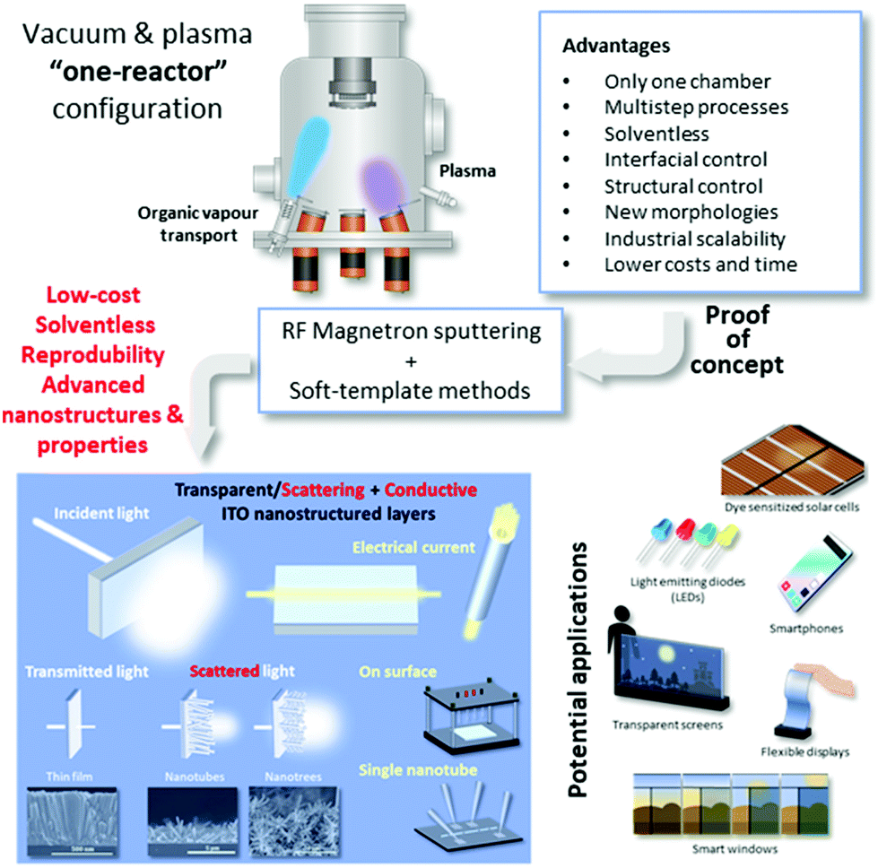 | ||
| Scheme 1 The one-reactor approach for scalable vacuum and plasma deposition of nanostructured TCOs for diverse applications. The schematic includes advantages of the procedure for the development of 1D and 3D nanotubes, the proof-of-concept carried out with a transparent conducting oxide, concretely ITO, and several examples of the foreseeable applications of such nanomaterials. | ||
As demonstrated below, our new proprietary approach allows:
(i) Integration of sequential and/or simultaneous fabrication/processing steps into the same reactor to reduce the number of vacuum chambers and minimize sample transfers between them (thus reducing hardware cost, processing time, and energy consumed in the process);
(ii) Production of every layer of the active system by a vacuum procedure (avoiding liquid solvents, reducing waste by-products, and increasing reproducibility and interface stability);
(iii) Generation of microstructure-tailored nanoarchitectures with excellent control of the interfacial composition of sequentially deposited materials with either sharp or gradual/graded interfaces including organic, polymeric, inorganic, and hybrid compositions.
Remarkably, our approach surpasses the most common TCO magnetron sputtering deposition by the unprecedented production of polycrystalline ITO nanotubes and nanotrees. These nanostructures feature tunable thickness and length, excellent optoelectronic properties, and low resistivity, which collectively make them promising candidates for optical random media in the visible (VIS) and near-perfect absorbers in the Near Infrared (NIR) ranges.
Results and discussion
One-reactor fabrication of ITO nanotubes and nanotrees. Microstructural and chemical characterization
We have fabricated the ITO layers and shells under two different working pressure conditions (see detailed information in the Experimental section). Thus, the acronym LP refers to the “low-pressure conditions” during the magnetron sputtering of the ITO, i.e. 5.0 × 10⁻³ mbar; meanwhile, HP labels the “high-pressure conditions”, i.e. 2.0 × 10⁻² mbar. However, it is worth stressing that both LP and HP can be considered mild vacuum conditions. The labels also inform on the morphology of the samples, differentiating between thin films (TF), nanotubes (NT), and nanotrees (NTrees). Fig. 1 and 2 show the representative SEM images of the step-by-step process for the formation of the nanostructures.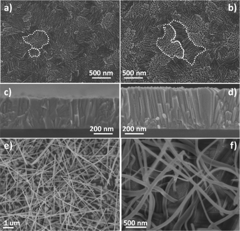 | ||
| Fig. 1 Steps 1 and 2 of the ITO nanostructure synthesis process. Representative SEM images including LP and HP thin films (a, c) and (b, d) respectively and ONW formation on the surface of the LP ITO film (e and f). Panels (c) and (d) show the cross-sectional images of the thin films. The dashed lines are included as a guide to the eye on the different sizes of the crystalline domains. | ||
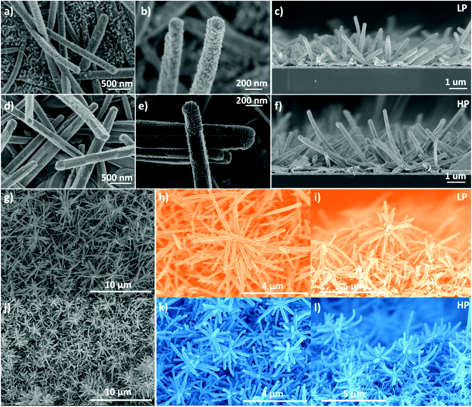 | ||
| Fig. 2 Supported ITO nanotubes and nanotrees manufactured by the scalable one-reactor approach. Representative SEM images including nanotubes (a–f) and nanotrees (g–l), with micrographs (a–c) and (g–i) corresponding to samples fabricated under LP conditions and (d–f) and (j–l) under HP conditions. Panels on the right-side display cross-sectional characteristic views of the samples. | ||
See Scheme S1 in the ESI† for a pictorial representation of the protocol. Fig. 1(a)–(d) show the comparison of the normal and cross-sectional views of the thin films prepared under the two Ar pressure conditions, LP (a and c) and HP (b and d). At first glance, they present the same morphology with triangular and elongated features coexisting on the surface but forming patches or domains. These domains contain motifs with similar morphology and orientation. Close inspection of the planar view images reveals that the size of these domains is larger for the HP conditions, i.e. we count a smaller number of differentiated domains for the same area as highlighted by the dashed lines bounding the crystalline domains for the two samples.
The cross-sectional views show two different types of morphologies with a characteristic columnar formation. Samples deposited under HP conditions present a better defined columnar cross-section (see panel c) than the LP films. The comparison of these two images also reveals that the growth rate for the HP condition is higher than that for the LP case, with growth rates of 5.3 ± 0.1 nm s−1 and 4.4 ± 0.2 nm s−1, respectively. These values are representative of the yield for the commercially available magnetron sputtering source that we have implemented (see Experimental) and comparable with the results in the literature for the deposition of ITO thin films.41 In the following experiments, we use this finding to deposit ITO films and shells with comparable final thicknesses for both HP and LP conditions.
The following step consists of the formation of phthalocyanine organic nanowires (ONWs) on an ITO thin film acting as the nucleation surface. For such purposes, in step 1, an ITO thin film is deposited under LP conditions with a thickness of ∼120 nm to form the “seed” growth surface. Such a thin ITO layer improves the overall lateral conductivity of the system. In step 2, the formation of the ONWs is carried out in the same reactor by placing a low-temperature evaporator facing towards the substrates (see the Experimental section). After several preliminary experiments, the pressure of Ar and temperature of the substrates were established at 1 × 10⁻³ mbar and 210 °C to form a high density of supported ONWs as shown in Fig. 1(e and f). The nanowires mostly present a square footprint with the mean width and length of 100 ± 30 nm and 4.0 ± 1.6 μm, respectively (see Fig. S1 and Table S1† for the statistics carried out by image analysis). The estimated density of ONWs is 6.5 ONWs μm−2. Such formation of ONWs on the surface of the ITO thin films deposited in the same reactor is the first step towards the demonstration of the “one-reactor” approach.
It is important to stress herein that by this procedure the substrate is not limited to an ITO thin film or surface. Thus, we have previously demonstrated the compatibility of this soft-template formation with a variety of supports, including metal and metal oxide layers and nanoparticles, polymers, and organic systems. This is also extended, for instance, to the direct formation of the ONWs on device architectures and pre-formed electrodes.37,38,42–44
In step 3, the ONWs are coated with ITO shells of exactly 175 nm of equivalent thickness under both LP and HP conditions. The yield of the deposition is given by the estimation of the ITO-shell thicknesses, calculated as 47 ± 10 nm for the low pressure and 65.5 ± 10 nm for the high pressure samples. Note that these values correspond to the differences between the radii of the nanotubes and the radii of the inner cores. The mean total thickness of the nanotubes is about 200 nm under both conditions. The panels (a) to (f) in Fig. 2 show the SEM images at different magnifications (see also Fig. S1 and Table S1†). From Fig. 2(b and e), it is easy to see a different growth for the two conditions. On the one hand, LP ITO nanotubes show a homogeneous morphology along their entire structure with non-defined domains. On the other hand, HP ITO nanotubes exhibit well-defined morphological domains, as an extension of such characteristics of the corresponding thin film microstructure. Although the alignment is not as pronounced as that found with the soft-template approach using plasma-enhanced chemical vapour deposition,36,50 the cross-sectional images suggest that the ITO nanotubes (Fig. 2c and f) present a slight vertical alignment in comparison with the organic nanowires (Fig. 1e and f).
In the final step, the leftovers of the organic nanowires remaining after the ITO deposition are easily removed by annealing at 350 °C under air or vacuum conditions (within the same reactor adding oxygen). The organic molecules evacuate the core through the pores of the ITO shell and substrate leaving no traces as we have previously shown by HAADF-STEM on ZnO and TiO2 nanotubes.44 This straightforward removal of the template is a key advantage of the method and will be also supported by the optical properties discussed below. Finally, the samples were annealed at 350 °C in Ar to ensure fine transparency (see the Experimental section).
Pursuing the sensing, photoelectrochemical and electrocatalytic applications of TCOs, it is imperative to generate highly interconnected, 3D arrangements and open nanostructures yielding high-surface-area electrodes. Hence, the next step is to fabricate three-dimensional (3D) ITO nanotubes or nanotrees (NTrees). For such purposes, steps 2 and 3 are repeated using the as-grown ITO nanotubes as substrates (see Scheme S1†). Fig. 2(g–l) presents the SEM images of these nanostructures. In both cases, LP (g–i) and HP (j–l), the morphology resembles a high density of branched nanotubes or nanotrees with a “trunk” surrounded by “branches” distributed on the lateral surfaces of the “trunks” (Fig. 2(i) and (l)). If we compare both nanostructures, it is obvious that LP nanotrees lead to longer sizes (Fig. 2(g) and (h)), whereas for HP samples, the branches are well distributed over all the substrates leading to smaller sizes (Fig. 2(j) and (k)) and a higher density than the LP sample. These differences arise from the diverse roughness and motifs on the surface of the primary nanotubes yielding such slightly different forms of organic nanowires.
With the extension of the protocol from 1D to 3D by simple iteration of the process, we further demonstrated that the one-reactor approach provides a straightforward way for the fabrication of complex systems by combining two different deposition techniques in the same reactor, i.e. the thermal evaporation of organic molecules and magnetron sputtering of a transparent conducting oxide. On the other hand, we proved that the soft-template procedure based on the use of single-crystalline ONWs as a supported 1D scaffold can be extended to the fabrication of shells by magnetron sputtering, one of the most industry-wide vacuum deposition processes.
The TEM images in Fig. 3 of individual nanotubes allow the detailed comparison of the morphology and crystalline structure for LP and HP deposition conditions. The lighter area along the axis of the nanotubes corresponds to the cavity left after the organic template sublimation. It is also possible to confirm the growth of columnar and triangular features from such an axis forming a conformal shell or wall that is characteristic of the nanotube morphology. The HP nanotubes show larger crystals (65 ± 6 nm) than LP ones (46 ± 6 nm), considering that the grains grow outwards from the template hole. The HRTEM images (Fig. 3(e) and (f)) provide information of the crystalline planes revealing multiple interplanar distances for the LP and HP conditions. The prevalent distances of 5.15 Å and 2.68 Å are related to the (2 0 0) and (4 0 0) planes for LP nanotubes, respectively. The distances of 4.32 Å and 3.05 Å for HP conditions correspond to (2 1 1) and (2 2 2) planes, respectively. These results are in good agreement with the XRD patterns of the reference thin films, supported nanotubes, and nanotrees presented in Fig. 3(g). Notably, the In2O3 crystalline structure was reproduced in all of them. We emphasize that the (2 1 1), (2 2 2), and (4 0 0) planes show the highest intensity. The crystal size (Fig. S2†) is generally lower than 100 nm as determined using the Scherrer approximation for all families of planes and under both deposition conditions. However, planes such as (2 1 1) in the HP thin film sample or (2 2 2) in the LP nanotube sample present larger sizes (168.5 and 178.7 nm, respectively). ITO nanotrees prepared under HP conditions display the same characteristic planes as their nanotube counterparts, indicating that both trunks and branches feature the same microstructure.
 | ||
| Fig. 3 High crystalline quality of the produced thin films, nanotubes and nanotrees. TEM (a–d) and HRTEM (e and f) micrographs of the ITO nanotube samples prepared under LP (left-side) and HP (right-side) conditions. Insets in (f) show the FFT (top) and enlarged view (bottom) of the framed areas of the HRTEM images. (g) XRD indexed diffractograms comparing the supported nanostructures and the reference thin films. | ||
We have also studied the crystalline texture using the textural parameter, Thkl, (see Fig. S2†). The deposition conditions lead to the formation of highly textured samples, with the preferential growth of planes (211) and (411) for the three types of samples prepared under both LP and HP conditions. These results demonstrate on the one hand that this synthetic approach produces highly crystalline nanotubes and, on the other hand, that the thin film microstructure is extended to the 1D and 3D nanostructures but at a reduced characteristic scale. Importantly, both columns and crystal domains are smaller for the nanotubes than for the reference thin films.
To elucidate the surface and “bulk” chemical composition of the ITO nanotubes, we carried out X-ray Photoelectron Spectroscopy (XPS) and Rutherford Backscattering Spectrometry (RBS) characterization studies. Fig. S3 and Table S3† summarize the spectra acquired for the different samples. Photo-electron peaks corresponding to In 4s, 3d, 3p, and 3s; Sn 3d and 3p; O 1s; C 1s; and Auger electron peaks (In MNN, O KLL and C KVV) have been labelled in the spectra. Besides, we quantitatively analysed the elemental composition using the peak zone spectra to obtain the atomic percent composition of the surface layer (Table S3†). We obtained that the ratio of Sn to Sn + In is 0.10 in the LP ITO nanotubes and 0.12 in HP ones. We can confirm that the target composition is reproduced in the surface layer of the LP NTs and it is slightly enriched in Sn for the HP conditions. In the RBS spectra in Fig. S3,† one can observe high-energy (1000–1400 keV) signals that correspond to ions backscattered upon interactions with Sn and In atoms. Furthermore, there are two distinctive spectral shapes in two different regions. For the high energy region (corresponding to the sublayer closest to the sample surface), the amount of counts is lower. This finding is in good agreement with a higher porosity related to the nanotube layer. The lower energy region (related to the layer closer to the substrate) presents a higher amount of counts, corresponding to the seed thin film layer formed at the interface with the substrate. For both the HP and LP conditions, the O to In + Sn ratio exceeds 1.5 at the interface with the substrate and gets closer to 2 at the nanotube layer. Such excess of oxygen might be associated with the presence of carbonaceous species.
Optical properties
As introduced above, the main application of ITO thin films is as a transparent conductive oxide in optoelectronic devices. Fig. 4(a and b) show the photographs of the samples at different stages of thin film, NT, and NTree fabrication. The as-prepared ITO thin films present high transparency under visual inspection (panel (a) on the left). Fig. 4(c) and (d) show the comparison of the UV-vis-NIR ballistic transmission spectra for ITO thin films deposited under LP (c) and HP (d) conditions. In both cases, the spectrum is divided into three sections. Firstly, one can see that transmittance in the UV region (λ < 400 nm) is low. This is related to the onset position of the absorption across the fundamental optical band gap (see Table 1, estimated by the Tauc plot). The intrinsic band gap for ITO is 3.53 eV,73 in our case, 3.54 eV and 3.42 eV, for the reference thin films deposited under LP and HP conditions, respectively. This difference might be related to the composition of the samples slightly enriched in Sn for the HP conditions in comparison with the LP case. Secondly, in the visible (VIS) range, both samples present the transmittance spectra featuring the interference fringes characteristic of transparent thin films. The refractive index and extinction coefficient wavelength dependence of these thin films were obtained by fitting these transmittance spectra with WVASE software using a Lorentz complex refractive index model with three oscillators (Table 1, see also Experimental).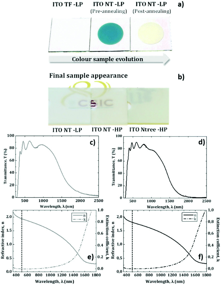 | ||
| Fig. 4 From transparent thin films to strong light scattering in 1D and 3D nanoarchitectures. (a and b) Photographs of the synthesized samples as labelled. Ballistic transmittance spectra and estimated refractive index and extinction coefficient (c) and (e) for LP and (d) and (f) for HP thin films. | ||
| Sample/measure | Transmittance, T ±0.5% | Refractive index, n | Extinction coefficient, k | Bandgap, BG (eV) |
|---|---|---|---|---|
| a All the fittings we carried out have an adjustment R2 value >0.99. | ||||
| ITO_TF-LP | 80 | 1.94 | 1.6 × 10⁻³ | 3.54 |
| ITO_TF-HP | 85 | 1.81 | 2.8 × 10⁻³ | 3.42 |
These values are in good agreement with previous reports.45–49 The extinction coefficients in the visible range (Fig. 4(e) and (f)) are very low for both samples, which is a desirable characteristic for the intended application of these films. It is worth stressing that the difference between the refractive indices (nLP > nHP) may be related to the higher porosity in the HP samples than in the LP samples, which is likely related to the more pronounced columnar growth (see Fig. 2). Finally, for wavelengths longer than 1000 nm, both spectra show an abrupt drop in the transmittance in the NIR range. This is related to the conductivity mechanism of ITO and, consequently, to the free-carrier absorption requiring the excitation by an IR photon of an electron at the bottom of the conduction band towards higher energy positions within the same band.1 Once the ONWs are formed, the sample becomes intense blue ((a)-middle) corresponding to the H2-phthalocyanine Q-Band absorption in the range between 600 and 700 nm (ref. 42) and remains bluish after the deposition of the ITO shell. The post-annealing treatment of the samples (see the Experimental section) completely removes the organic template leading to the white colour of the samples (Fig. 4(a) and (b)). In a good agreement, the UV-VIS-NIR spectra in Fig. S4† comparing nanotube samples deposited under LP and HP conditions are dominated by scattering effects in the visible range that reduce their transparency. Besides, the transmittance spectra show the expected drop in the NIR range corresponding to highly conductive ITO nanomaterials.45–49 Such a whitish dispersive colour of the nanostructured samples is important for applications of these nanoelectrodes in photoelectrochemical and light-emitting devices.
To explore the utility of our nanostructures in this context, we carried out an additional optical characterization of the NT and NTree samples prepared under high-pressure conditions making use of an integrating sphere (LP Ntrees are included herein for the sake of comparison, Fig. S5† shows the corresponding results for LP thin films and nanotubes). Fig. 5 shows the total and diffuse transmittances (TT, solid line and TD, dashed line) (a and b), total and diffuse reflectances (RT, solid line and RD, dashed line) (c and d), and the absorptance (e and f), i.e. the ratio between the light absorbed by the material to intensity of the incident light, for the layers prepared under HP conditions. The diffuse spectra take into account light scattered in all directions except for the specular and ballistic effects, and thus, represent an integrated measure of a single or multiple scattering events. The difference between the total and diffuse components results in the direct value, i.e. specular reflectance and ballistic transmittance, meaning that the light propagation remains along the same straight line as the incident light. In this case, for NTs and Ntrees, we cannot estimate the optical band gap because the absorption edge in the 400–500 nm range is already dominated by strong scattering effects. However, it is worth noting that the transmission edge for the NTree samples is red-shifted with respect to the nanotubes and thin films (Fig. 5(a)), and this effect is also appreciable in the absorptances presented in panel (e). We hypothesize that this observation might be related to the reduction in the bandgap in the nanotree samples.
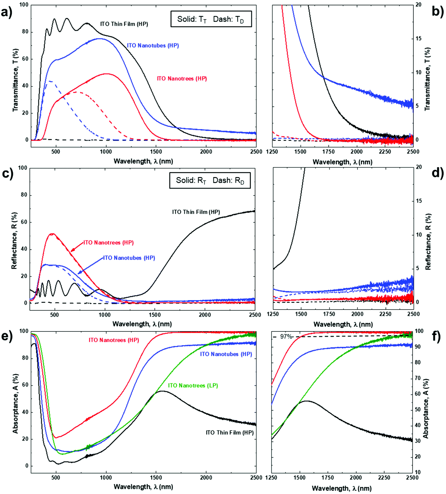 | ||
| Fig. 5 Nanotubes and nanotrees working as Random Optical Materials in the VIS and Ultra Broadband Perfect Absorbers in the NIR. UV-vis-NIR spectra of ITO HP samples: (a and b) total and diffusive transmittance (TT and TD) and (c and d) reflectance (RT and RD). (b) and (d) are the zoomed-in view of the NIR range corresponding to (a) and (b) respectively; (e) absorptance. The corresponding spectrum for LP NTrees is included for the sake of comparison. | ||
Concerning the transmittance, the spectrum for the thin film depicts a nearly zero value for the diffuse component. In the case of ITO NTs and Ntrees, the curves for the total (TT, solid line) and diffuse (TD, dashed line) transmittance overlap at low wavelengths and separate above 390 nm and 560 nm for the nanotubes and nanotrees, respectively. This means that for the shorter wavelengths, the direct transmittance is close to zero, thus validating the extremely high light dispersion of the ITO NTs and NTrees. The total transmittance decreases from thin films to nanotubes, and from nanotubes to nanotrees. The highest transmittances of the 1D and 3D nanostructures in the 750 to 1250 nm range.
Looking at the reflectance spectra, we find a similar behaviour for the thin film, i.e. the low reflectivity of this sample corresponds to the specular component, with no contribution from scattered light. For the NT sample, the diffuse component is the most predominant below 500 nm (dashed and solid lines overlap at low wavelengths). Above this value, the reflectance is still dominated by the diffuse component although there is a significant contribution from the specular reflectance. Strikingly, for the ITO NTrees both total and diffuse reflectance spectra overlap in the VIS and NIR ranges. In the VIS range, the total reflectance increases from the thin film to the nanotubes and from the nanotubes to the nanotrees, with a maximum value of 50%. It is worth emphasizing that both the nanotubes and nanotrees act as scattering centers for the incident light, behaving as random optical materials. Thus, in the visible region, diffuse light reflection (in different directions from the specular one) dominates. Likewise, a very significant fraction of the transmitted light is also diffuse (in different directions from the ballistic direction).
These results have two promising applications. First, we have developed an extremely efficient diffusor. Fig. S6† shows the comparison of the Haze factors ([diffuse transmission/total transmission] × 100) estimated for the three types of samples in the range between 400 and 800 nm which yields values higher than 80% for the nanotree samples. This is an outstanding value with potential applications,50–52 for example, in photocatalytic processes such as water splitting where high light scattering increases the light trapping.53 In the case of light emission, white-colour nanoelectrodes can be used in the white light LED technology where the light-scattering properties of the phosphors are usually utilized as a diffusive medium to obtain uniform emission without hot spots or angular colour distribution.54 Second, these scattering layers can be implemented as electrodes in photovoltaic and light-emitting devices. The latter application demands higher intensities of the emitted light by enhancing the external quantum efficiency (EQE). Hence, the use of scattering sheets (external or internal) is common, for example, in devices such as OLEDs to improve the outcoupling efficiency of light generated in the device. In our case, the scattering shell would at the same time serve as an electrode to improve light outcoupling efficiency, as it has been previously reported for metal networks.55 The next step is to study the reflectance and transmittance spectra for the 1D and 3D nanostructures in the NIR range. As explained above, the low transmittance of the samples in this range is related to the conductivity mechanism in doped wide-bandgap metal oxides. Therefore, in good agreement with the Drude equivalent model,56 the ITO thin film transmittance drops below a certain value becoming almost zero for wavelengths above 2000 nm (Fig. 5(a and b)). In constrast, the reflectance increases for the NIR range reaching up to 60% for long wavelengths (Fig. 5(c and d)). The trend is similar for the transmittance spectra of the nanotubes and nanotrees with a much sharper drop in the case of the 3D nanostructures that present a total transmittance below 2% for wavelengths longer than 1500 nm and nearly zero above 1750 nm (Fig. 5(b)). However, the reflectance of the 1D and 3D ITO nanostructures decreases in the NIR. Consequently, these samples show extremely low values of reflectance in this range, namely below 1% for the nanotrees (Fig. 5(d)) in the range from 1250 to 2500 nm, thus acting as broadband antireflective coatings. This characteristic is more pronounced for the NTrees and NTs produced under HP conditions (see Fig. S5† for comparison), thus, the absorptances shown in Fig. 5(e and f) for the HP samples increase dramatically as the wavelength increases in the NIR region of the spectra. The 1D samples feature a plateau of 90–92% for wavelengths higher than 1800 nm meanwhile for the 3D samples the plateau appears at even higher levels of 99–100% for wavelengths above 1600 nm. In both cases, especially in the latter case, the ITO samples perform like perfect light absorbers in the infrared, inhibiting the transmission and reflection of electromagnetic waves. The perfect absorption (PA) of these ITO supported nanostructures might be attributed to the near-zero values of the refractive index in the NIR region, due to the near-zero values of the electric permittivity in this spectral region.57 Importantly, the ITO presents a characteristic epsilon-near-zero (ENZ) point in the NIR whose position is a function of the doping level.58 Several authors have reported PA in ITO thin films on metallic substrates,59,60 combined with plasmonic gratings.61 Yoon et al. reported a broad-band PA in the range 1450–1750 nm by stacking ITO films with different doping levels under attenuated total reflection conditions. Other authors have demonstrated electrically controlled absorption modulation of ITO metafilms in the ENZ region.61,62 However, very different from the previous reports, our supported nanotube and nanotree structures deposited under HP conditions show a flat and broad-band complete absorptance in the range 1600–2500 nm and do not show multiple PA maxima. Such a behaviour most likely implies that there are different levels of doping in the nanostructures comprising the ITO-NT and ITO-NTree layers. However, the relationships between the level of doping, the nanostructure (nanotubes and nanotrees), and their specific spatial distribution (nanotube and nanotree thicknesses and lengths, densities, and branching degrees) determining the ENZ properties of the nanostructured ITO and potential electrical tunability need further studies in order to fully understand the broadband PA observed. Previous attempts to develop broadband near-perfect absorption surfaces relied on the use of metamaterials, surface plasmons, 2D materials, or resonant optical cavities.64–70 Common shortcomings of these efforts are narrow spectral bands and complex fabrication procedures with limited scalability for large-area applications.29 Recently, several authors have reported alternative solutions based on the formation of one-dimensional nanomaterials such as carbon nanotubes, Si nanoarrays, Cu nanowires, and ITO nanowires.29 In our case, the characteristics of the supported nanotubes and nanotrees allow the straightforward use of these nanomaterials in a lithography-free process and on a broad variety of substrates without additional processing, patterning, or special optical arrangements.
Electrical characterization of layers and single NTs
Fig. 6 and Table 2 summarize the most important findings regarding the electrical characterization of the samples. The aim is to elucidate the two key electrical resistances, one corresponding to the layer of NTs and NTrees supported on the ITO decorated substrates and the other one corresponding to the individual nanotubes. Fig. 6(a) shows the I–V curves obtained for the five types of samples, including the LP and HP thin films determined by a four-probe macroscopic platform (see the Experimental section). All these curves present an ohmic linear relationship between the current (I) and the voltage (V) in the studied range (−0.5 and 0.5 V) with different slopes corresponding to the variations in resistance (R) of the samples.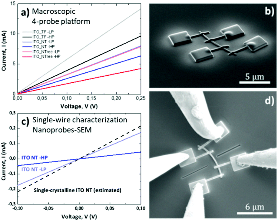 | ||
| Fig. 6 Competitive conductivity and resistivity of the highly textured thin films and nanotubes. (a) 4-Probe electrical characterization of ITO thin film (LP and HP), nanotubes (LP and HP) and nanotrees (HP) I–V macroscopic measurements and (c) I–V curves comparative between ITO nanotube (LP and HP) nanoscopic measurements, the estimated curve for a single-crystalline ITO nanowire has been included as a ref. 24. (b) Representative SEM images of the electrical nanoscopic characterization by deposition of four Pt pads by FIB and (d) in situ SEM microprobe measurements. | ||
| Sample/measure | Resistance, R (Ω) | Resistivity, ρ (Ω cm) |
|---|---|---|
| R sheet (Ω sq−1) | ||
| ITO_TF-LP | 1.93 ± 0.09 | (2.48 ± 0.12) × 10−4 |
| 16.1 ± 0.8 | ||
| ITO_TF-HP | 3.29 ± 0.24 | (4.3 ± 0.4) × 10−4 |
| 27.4 ± 2.0 | ||
| ITO_NT-LP | 4.2 ± 0.2 | — |
| ITO_NT-HP | 5.6 ± 0.4 | — |
| ITO_NTree-LP | 3.7 ± 0.3 | — |
| ITO_NTree-HP | 6.51 ± 0.13 | — |
| Sample/measure single wire | Resistance, R (Ω) | Resistivity, ρ (Ω cm) |
|---|---|---|
| ITO_NT-LP | 480 ± 110 | (3.5 ± 0.9) × 10−4 |
| ITO_NT-HP | 180 ± 40 | (15 ± 7) × 10−4 |
Table 2 shows the estimated R values with the lowest limits corresponding to the thin film samples. Sheet resistance and resistivity of these samples are competitive with the ITO films deposited by RF magnetron sputtering.45–49 Besides, the sheet resistance and resistivity of the ITO thin film prepared under LP conditions are almost two times lower than those of the HP sample. The macroscopic resistances of the nanotube samples follow the same trend, being in both cases higher than those for the thin film counterparts though still presenting quite low values. Impressively, the resistance for the LP Ntrees are lower than those for the 1D counterpart. This improvement in the lateral connectivity can be directly linked to the formation of long secondary branches (see Fig. 2) which connect adjacent ITO trunks. Such a characteristic is not as pronounced under the HP conditions producing shorter but numerous secondary nanotubes showing high contact resistance from one tree to the other. Please note that the connectivity between the nanotubes and the substrate is ensured in this case as the shell and the seed layers present the same composition, i.e. ITO. Thus, Fig. S7† presents the top view and cross-sectional micrographs for a low-density area where it is visible that the ITO layer deposited in step 3 working as the nanotubes’ shell forms also a continuous layer on top of the substrate connecting the nanotubes with the seed layers (formed in step 1) and among them. Moreover, the cross-sectional image reveals how the second layer (forming the shells) grows continuously on top of the seed one, allowing for an intimate electrical contact between substrate and nanotubes.
It must be stressed at this point that the estimation of sheet resistance and resistivity is not straightforward for the 1D and 3D nanostructured samples because of the difficulty inherent to the precise estimation of the conducting cross section area. Therefore, we note that the comparison between the resistances in those cases is only semi-quantitative. Thus, the accurate elucidation of the NT electrical conductivity requires the characterization in a single-wire approach, i.e. contacting the NTs as individual items.
For the advanced single-wire characterization, the NTs were removed from the substrate and deposited flat on Si (100) wafers as detailed in the Experimental section. Fig. 6(b) shows the characteristic SEM image taken after the FIB deposition of four equivalent Pt electrodes with areas around 3 × 3 μm2. Nanotubes with similar diameters and lengths are brought into contact aiming for a fair comparison. In the second step, the ITO nanotubes are characterized by a 4 nanoprobe platform from Kleindiek Nanotechnik installed in the SEM (Fig. 6(d)). I–V curves in Fig. 6(c) are representative of both types of NTs. Here, we note that the corresponding values in Table 2 were calculated after analysis of three different NTs from each condition and five I–V curves. In all the cases, linear current versus voltage curves were observed in all measurements. In good agreement with the previous results, the nanotube resistivity for the HP conditions is higher than that for the LP. The resistivity for both samples is in a very low range, and in the LP case, it is comparable to the reported values for single-crystalline ITO NWs fabricated by VLS (2.4 × 10⁻⁴ Ω cm)23 (included in panel c) as a reference value).
At this point, it is important to stress the differences of our structures with respect to the 1D and 3D single-crystal ITO nanostructures reported in the literature, mostly formed by the catalyst driven mechanisms.21–23 Thus, Table 3 includes the comparison with reported methods and protocols for the fabrication of ITO thin films and low dimensional materials.16,21–23,26–28,28–30,71 First of all, although we produce polycrystalline nanotubes, the results of the single-wire electrical characterization support that the high crystalline quality and good connectivity between ITO grains forming the NT shells allow an effective carrier transport along the NT length. Besides, in the above examples, all the nanotubes are domed; however, the same procedure can be modified to generate open-ended nanotubes by simply increasing the temperature rate slope during the evacuation of the organic template (see additional information elsewhere).44 Secondly, the thickness and length of the nanotubes are adaptable and controllable by tuning the ONW length and the ITO shell deposition time. Thus, although the thickness settled for the nanotubes and nanotrees in this article is too thick (200 nm) to allow for the compatibility with flexible supports and devices, it can be straightforwardly reduced in order to improve the performance of these nanostructures for such final applications.
| Synthesis method | Type of nanostructure | Synthesis temperature (°C) | Transmittance (visible range) (%) | Resistivity (Ω cm) | R sheet (Ω sq−1) | Ref. |
|---|---|---|---|---|---|---|
| Magnetron sputtering | Thin film | |||||
| LP | 350 | >85 (thickness 400 nm) | 2.4 × 10⁻⁴ | 16.1 | This work | |
| HP | 4.3 × 10⁻⁴ | 27.4 | ||||
| Sputtering | Thin film | — | 85 (thickness 100 nm) | — | 14–16 | Commercially available (Ossila) |
| Sputtering | Thin film | — | 84 (thickness 120–160 nm) | — | 8–12 | Commercially available (Sigma Aldrich) |
| Soft-template coated by MS | Nanotubes | |||||
| LP | 350 | ∼70 | 3.5 × 10⁻⁴ | — | This work | |
| HP | ∼70 | 15 × 10−4 | — | |||
| Soft-template coated by MS | Nanotrees | |||||
| LP | 350 | ∼50 | — | — | This work | |
| HP | ∼40 | — | — | |||
| Self-catalytic VLS | Nanowires | 920 | — | — | — | 21 |
| VLS epitaxial growth | Nanowires | 900 | — | — | — | 43 |
| Vapour transport | Nanowires | 840 | ∼80 | 2.4 × 10⁻⁴ | 6.4 | 23 |
| Au-Assisted catalytic, thermal evaporation | Nanowires | 700 | — | — | — | 72 |
| Self-catalytic VLS | Nanowires | 300 | >80 | — | ∼100 | 22 |
| Hard-template coated by ALD + IAD | Nanotubes | 450 | — | — | ∼Braided copper cables | 27 |
| Hard-template coated by electron beam evaporation | Nanotubes | 350 | ∼80 | — | 259.4 | 26 |
| Polymer-assisted catalytic growth by e beam Evap | “Nanotrees” | 450 | 70–95 | — | 5–193 | 29 |
| Polymer-assisted catalytic growth by e-beam Evap | Nanowires | 300 | ∼80 | ∼150 | 28 | |
| Polymer-assisted catalytic growth by e beam Evap | Nanowires | 300 | 90 | — | 200 | 71 |
| Soft-template coated by electrophoretic deposition | Nanowires | 500 | — | — | — | 30 |
As an additional advantage over VLS, VS, and other template alternatives, the formation of nanotrees is straightforward by repeating the deposition protocol as many times as desired. Moreover, the growth does not require any modification of the template or the generation of defects on the ITO single crystal surface. Finally, the conformal character of the ITO shell and formation of the ITO layer in the free area among the nanotubes may improve the lateral connectivity of the 1D and 3D nanostructures in comparison with the single-crystal counterparts.
Experimental
Substrates
We have fabricated ITO thin films, 1D, and 3D nanostructures supported on different substrates attending to the characterization technique requirements. In general, for each experiment, a set including the following substrates was covered: glass slides, fused silica slides, (100) single crystalline P-type doped silicon wafers, and (100) single crystalline intrinsic silicon wafers.Synthesis
ITO thin films (ITO_TF) were deposited on Si (100), and fused silica under two conditions. The deposition method was magnetron sputtering under two deposition conditions addressed as low pressure, LP, and high pressure, HP. The pressure was regulated using a butterfly valve and controlled using a Pirani pressure meter, the Ar fluxes using a mass flow controller, and the deposition rates and thicknesses using a quartz microbalance located at a close position from the substrates. Cylindric magnetron with a 3′′ ITO disc target (SnO2 10 wt% doped In2O3) (Kurt J. Lesker Company) was excited under radiofrequency (13.5 MHz pulses) and argon plasma, with a low pressure (LP) of 5 × 10⁻³ mbar, an Ar flux of 30 cm3 min−1, and a source power of 75 W, and a High Pressure (HP) of 2 × 10⁻² mbar, an Ar flux of 45 cm3 min−1, and a source power of 150 W. The substrate holder temperature was controlled at 350 °C with a spinning velocity of 20 rpm.Secondly, ITO nanotubes (ITO_NTs) were formed on the surface of the different substrates following the fabrication method that consists of four steps (see Scheme S1†): (i) formation of nucleation centers, (ii) growth of the supported organic nanowires, (iii) formation of the ITO shell and (iv) evacuation of the organic core from the 1D hybrid core@shell nanostructures to leave an empty ITO nanotube. Step (i) the features on the surface of the substrate act as NW growth nucleation centres; in this work, the seed or nucleation layer is an ITO thin film deposited by magnetron sputtering under LP conditions to increase the surface roughness. Substrate temperature for the deposition of the ONWs was 210 °C meanwhile for the formation of the ITO shell, the temperature was increased up to 350 °C. Finally, all the samples were annealed at 350 °C in an Ar atmosphere to achieve steady-state conditions.
Characterization
Three different SEM instruments were utilized: an S4800 microscope from Hitachi for the overall microstructural characterization; a GeminiSEM 300 microscope from Zeiss utilized during the 4-probe electrical characterization (see below) and, an FEI Helios Nanolab 650 for the ITO NT assembly for single-wire nanoelectrode characterization. The micrographs were treated with ImageJ free available software to carry out measurements and statistical analysis of different magnitudes such as film thickness, nanotubes diameter, and length.For the TEM characterization, NTs were removed from the substrates by scratching with a diamond tip and then deposited in a holey carbon Cu grid. Bright field and High Resolution (HREM) electron microscopy images were acquired in a JEOL 2100Plus operated at 200 kV equipped with a LaB6 filament and a CCD camera (Gatan). The HRTEM micrographs were analyzed with the TIA Reader software generating a digital diffraction pattern to measure interplanar distances and to index them. The crystalline structure was analyzed using an X-Ray Diffraction (XRD) spectrometer in a Panalytical X'PERT PRO model operating in the θ–2θ configuration and using the Cu Kα (1.5418 Å) radiation as an excitation source [PANalytical X'Pert HighScore database: Indium Oxide; reference code: 00-006-0416]. The crystallite size was determined with PANalytical X'Pert HighScore Plus software, which applies the Scherrer equation for the calculations. The texture coefficients or Lotgering factors Thkl were calculated applying the equation from ref. 63. The surface In/Sn ratio was determined using an X-ray photoelectron spectroscopy (XPS) PHOIBOS 100 hemispheric multichannel analyzer from SPECS using the Al Kα radiation as an excitation source. General and peak spectra were acquired with a pass energy of 50 and 30 eV, respectively. The samples were characterized after the annealing treatment without any additional surface conditioning. The atomic percentage of quantification was estimated using CASA software. Rutherford backscattering spectroscopy (RBS) was performed at the 3 MV Tandem Accelerator of the National Center for Accelerators (Sevilla, Spain) with an alpha beam of 1.6 MeV and a passivated implanted planar silicon detector at a 165° scattering angle. The RBS spectra were analyzed using the SIMNRA software.
The optical characterization was done by UV-vis-NIR spectroscopy (UV-vis-NIR) in the transmittance and reflectance modes. In this technique, a wavelength sweep from 2500 to 200 nm was set to analyze the near-infrared absorption, the visible range behaviour, and the gap presence in the UV region. The transmittance spectrum could be fitted to obtain the dependence of the refraction and extinction coefficients on radiation wavelength, which was implemented by applying a Lorentz Model of three oscillators with the optical analysis software by J.A. Woollam (WVASE®) (https://www.jawoollam.com/ellipsometry-software/wvase). Two UV-vis-NIR spectrophotometers were utilized, a PerkinElmer Lambda 750 UV/vis/NIR model for specular transmittance and reflectance and an Agilent Technologies Cary 5000 Uv-Vis-NIR equipped with an integrating sphere to acquire absorptance A, diffuse and total transmittance (TD and TT), diffuse and total reflectance (RD and RT).
The electrical characterization was carried out at two different levels aiming at both, macro- (nanotubes forming supported layers) and nano- (individual nanotubes) scales. In both cases, the 4-point probe method was utilized. The details on the estimation of resistivity and sheet resistance are shown in ESI Section S8.† The source meter was a Keithley 2635A system with a resolution in the range of 100 pA. The measurements were performed for the thin film and nanotube layer samples deposited on fused silica substrates. The equivalent characterization for individual nanotubes requires additional processing of the samples to contact the NTs using microscopic electrodes. This step enables the four nanoprobe electrical measurements assisted by SEM. For this purpose, the ITO NTs are removed from the substrate by scratching with a diamond tip and pressing the scratched area sample against a Si (100) intrinsic piece (note that these pieces present a native SiO2 layer acting as an electrical insulator).
The Focused Ion Beam (FIB) technique is used to form Pt patches and pathways with the controlled size and thickness coming in contact with the NT in four different points along its length. The equipment used was an FEI Helios Nanolab 650. The experimental FIB conditions: 30 kV and 40 pA. Contact dimensions: 4 × 0.14 × 0.50 μm (wire) and 2.5 × 3 × 0.3 μm (square). Precursor: Methyl cyclopentadienyl trimethyl platinum ((CH3)3Pt(CpCH3)). After the nanostructured electrode fabrication, the samples were characterized in the Zeiss Gemini SEM 300 equipped with four Kleindiek manipulators and nanoprobes (see Fig. S8†).
Conclusions
We have synthesized ITO thin films by magnetron sputtering operating under low- and high-pressure conditions (LP and HP, respectively) with a transparency in the visible range above 80% and low resistivity (ρ < 5 × 10⁻⁴ Ω cm). These values are very competitive with the previous reports based on RF and DC sputtering deposition. We have synthesized crystalline ITO nanotubes and nanotrees with crystal sizes lower than 170 nm, homogeneously distributed along the nanotube cavity, and highly textured. In parallel, we have revealed the advantages of the combination of the one-reactor method and the use of ONWs as 1D soft-templates supported on processable and scalable substrates. In comparison with previous articles dealing with such a protocol for plasma enhanced chemical vapour deposition (PECVD) of metal oxide shells,35–38,43,44 herein, we take a leap forward towards the application of magnetron sputtering, a different physical vapor deposition method typically characterized by a lower conformality but widely utilized in the industry. We show how the process is extendable to the fabrication of transparent conductive oxide (TCO) nanotubes which can be applied as foundations for photovoltaics, photocatalysis, optoelectronics and nanosensors. XPS, XRD, and UV-VIS-NIR results are in good agreement with the formation of highly conductive nanostructures with high absorbance in the NIR. The estimated values for sheet resistance and resistivity indicate that these nanostructured electrodes meet the expectations for their implementation in light-emitting devices and photoelectrochemical processes. Besides, we have demonstrated the potentiality of 1D and 3D nanostructures as optical random media in the VIS range and ultra-broadband perfect absorbers in the range 1600–2500 nm. Meanwhile, the LP conditions produce layers with a higher refractive index, and the optical properties of the HP NTs and NTrees in the NIR make these latter experimental conditions more interesting within the field of perfect absorbers. In constrast, the outstanding conductivity revealed under single-wire premises and the reduction of the lateral resistance contact for the LP NTs and NTrees respectively endow the nanomaterials produced under LP with critical features for their implementation in optoelectronic systems. Thus, the results gathered in this work open the way for applications that require effective control over light absorption/emission including renewable energy harvesting, selective electromagnetic absorption, selective thermal emission, and infrared stealth with potential impacts in the defense, renewable energy, and aerospace industries. In all these cases, our new approach can be used for a wide variety of substrates without the need for any structural patterning.Author contributions
A. Borrás, A. Barranco, J. R. Sanchez-Valencia and K. Ostrikov: conceptualization. A. Borrás, A. Barranco, and J. R. Sanchez-Valencia: funding acquisition. A. Borrás, J. Castillo-Seoane, and J. Gil-Rostra: writing original draft. All the authors were involved in the investigation, methodology, validation and reviewing and editing of the article.Conflicts of interest
There are no conflicts of interest to declare.Acknowledgements
We thank the AEI-MICINN (PID2019-110430GB-C21 and PID2019-109603RA-I0), the Consejería de Economía, Conocimiento, Empresas y Universidad de la Junta de Andalucía (PAIDI-2020 through projects US-1263142, ref. AT17-6079, P18-RT-3480), and the EU through cohesion fund and FEDER 2014–2020 programs for financial support. JS-V thanks the University of Seville through the VI PPIT-US and the Ramon y Cajal Spanish National programs. K. O. acknowledges partial support from the Australian Research Council. We thank the following centers for advanced characterization: the Supercomputing and Bioinnovation Center from the University of Malaga, XPS service from ICMS, the CITIUS from the University of Seville, and the High resolution SEM service from University Pablo de Olavide (UPO). GL thanks the funding from the EU H2020 program for the grant agreement 715832 (ERC Starting Grant Nanophom). The project leading to this article has received funding from the EU H2020 program under grant agreement 851929 (ERC Starting Grant 3DScavengers).Notes and references
- X. Yu, T. J. Marks and A. Facchetti, Nat. Mater., 2016, 15, 383–396 CrossRef CAS PubMed.
- K. Ellmer, Nat. Photonics, 2012, 6, 809–817 CrossRef CAS.
- M. Morales-Masis, S. D. Wolf, R. Woods-Robinson, J. W. Ager and C. Ballif, Adv. Electron. Mater., 2017, 3, 1600529 CrossRef.
- S. Ye, A. R. Rathmell, Z. Chen, I. E. Stewart and B. J. Wiley, Adv. Mater., 2014, 26, 6670–6687 CrossRef CAS PubMed.
- Z. Ma, Z. Li, K. Liu, C. Ye and V. J. Sorger, Nanophotonics, 2015, 4, 198–213 CAS.
- J. Liu, D. Jia, J. M. Gardner, E. M. J. Johansson and X. Zhang, Mater. Today Energy, 2019, 13, 152–185 CrossRef.
- D. S. Hecht, L. Hu and G. Irvin, Adv. Mater., 2011, 23, 1482–1513 CrossRef CAS PubMed.
- N. Sone, A. Suzuki, H. Murakami, N. Goto, M. Terazawa, W. Lu, D.-P. Han, K. Iida, M. Ohya, M. Iwaya, T. Takeuchi, S. Kamiyama and I. Akasaki, Phys. Status Solidi A, 2020, 217, 1900715 CrossRef CAS.
- Y. Hou, L. Wang, X. Zou, D. Wan, C. Liu, G. Li, X. Liu, Y. Liu, C. Jiang, J. C. Ho and L. Liao, Small, 2020, 16, 1905609 CrossRef CAS.
- J. Jung and D.-H. Kim, J. Alloys Compd., 2020, 823, 153648 CrossRef CAS.
- Z. Kordrostami and A. Yadollahi, Opt. Commun., 2020, 459, 125059 CrossRef CAS.
- D. van Dam, N. J. J. van Hoof, Y. Cui, P. J. van Veldhoven, E. P. A. M. Bakkers, J. Gómez Rivas and J. E. M. Haverkort, ACS Nano, 2016, 10, 11414–11419 CrossRef CAS PubMed.
- E. N. Dattoli and W. Lu, MRS Bull., 2011, 36, 782–788 CrossRef CAS.
- X. Liu, X. Liu, J. Wang, C. Liao, X. Xiao, S. Guo, C. Jiang, Z. Fan, T. Wang, X. Chen, W. Lu, W. Hu and L. Liao, Adv. Mater., 2014, 26, 7399–7404 CrossRef CAS PubMed.
- S. Zhao, D. Choi, T. Lee, A. K. Boyd, P. Barbara, E. Van Keuren and J. Hahm, J. Phys. Chem. C, 2015, 119, 14483–14489 CrossRef CAS PubMed.
- Q. Wan, P. Feng and T. H. Wang, Appl. Phys. Lett., 2006, 89, 123102 CrossRef.
- C. O'Dwyer, M. Szachowicz, G. Visimberga, V. Lavayen, S. B. Newcomb and C. M. S. Torres, Nat. Nanotechnol., 2009, 4, 239–244 CrossRef PubMed.
- M. Shariati, Biosens. Bioelectron., 2018, 105, 58–64 CrossRef CAS PubMed.
- X. Y. Xue, Y. J. Chen, Y. G. Liu, S. L. Shi, Y. G. Wang and T. H. Wang, Appl. Phys. Lett., 2006, 88, 201907 CrossRef.
- X. Feng, X. Feng, J. Liu, J. Liu, W. Yang, W. Yang, X. Yu, X. Yu, S. Jiang, S. Jiang, S. Jiang, T. Ning, T. Ning, J. Liu, J. Liu and J. Liu, Opt. Express, 2020, 28, 1554–1560 CrossRef CAS PubMed.
- Y. Q. Chen, J. Jiang, B. Wang and J. G. Hou, J. Phys. D: Appl. Phys., 2004, 37, 3319–3322 CrossRef CAS.
- R. Pruna, M. López and F. Teixidor, Nanoscale, 2018, 11, 276–284 RSC.
- J. Gao, R. Chen, D. H. Li, L. Jiang, J. C. Ye, X. C. Ma, X. D. Chen, Q. H. Xiong, H. D. Sun and T. Wu, Nanotechnology, 2011, 22, 195706 CrossRef CAS PubMed.
- Q. Wan, M. Wei, D. Zhi, J. L. MacManus-Driscoll and M. G. Blamire, Adv. Mater., 2006, 18, 234–238 CrossRef CAS.
- J. Li, L. Hu, J. Liu, L. Wang, T. J. Marks and G. Grüner, Appl. Phys. Lett., 2008, 93, 083306 CrossRef.
- M. D. Dickey, E. A. Weiss, E. J. Smythe, R. C. Chiechi, F. Capasso and G. M. Whitesides, ACS Nano, 2008, 2, 800–808 CrossRef CAS.
- A. B. F. Martinson, J. W. Elam, J. Liu, M. J. Pellin, T. J. Marks and J. T. Hupp, Nano Lett., 2008, 8, 2862–2866 CrossRef CAS PubMed.
- Q. Li, S. Wang, M. Zhang, L. Feng, X. Su, W. Ding, Y. Li and F. Yun, Sol. Energy, 2018, 173, 590–596 CrossRef CAS.
- Q. Li, Z. Tian, Y. Zhang, Z. Wang, Y. Li, W. Ding, T. Wang and F. Yun, Sci. Rep., 2019, 9, 4983 CrossRef.
- H.-W. Wang, C.-F. Ting, M.-K. Hung, C.-H. Chiou, Y.-L. Liu, Z. Liu, K. R. Ratinac and S. P. Ringer, Nanotechnology, 2009, 20, 055601 CrossRef PubMed.
- L. Li, S. Chen, J. Kim, C. Xu, Y. Zhao and K. J. Ziegler, J. Cryst. Growth, 2015, 413, 31–36 CrossRef CAS.
- Y. Xie, D. Kocaefe, C. Chen and Y. Kocaefe, J. Nanomater., 2016, 2016, 11 Search PubMed.
- A. Borras, M. Aguirre, O. Groening, C. Lopez-Cartes and P. Groening, Chem. Mater., 2008, 20, 7371–7373 CrossRef CAS.
- A. L. Briseno, S. C. B. Mannsfeld, S. A. Jenekhe, Z. Bao and Y. Xia, Mater. Today, 2008, 11, 38–47 CrossRef CAS.
- A. N. Filippin, V. López-Flores, T. C. Rojas, Z. Saghi, V. J. Rico, J. R. Sanchez-Valencia, J. P. Espinós, A. Zitolo, M. Viret, P. A. Midgley, A. Barranco and A. Borras, Chem. Mater., 2018, 30, 879–887 CrossRef CAS.
- M. Macias-Montero, A. N. Filippin, Z. Saghi, F. J. Aparicio, A. Barranco, J. P. Espinos, F. Frutos, A. R. Gonzalez-Elipe and A. Borras, Adv. Funct. Mater., 2013, 23, 5981–5989 CrossRef CAS.
- N. Filippin, J. Castillo-Seoane, M. C. López-Santos, C. T. Rojas, K. Ostrikov, A. Barranco, J. R. Sánchez-Valencia and A. Borrás, ACS Appl. Mater. Interfaces, 2020, 12, 50721–50733 CrossRef CAS.
- A. N. Filippin, J. R. Sanchez-Valencia, X. Garcia-Casas, V. Lopez-Flores, M. Macias-Montero, F. Frutos, A. Barranco and A. Borras, Nano Energy, 2019, 58, 476–483 CrossRef CAS.
- A. N. Filippin, J. R. Sanchez-Valencia, J. Idígoras, T. C. Rojas, A. Barranco, J. A. Anta and A. Borras, Nanoscale, 2017, 9, 8133–8141 RSC.
- J. M. Obrero, A. N. Filippin, M. Alcaire, J. R. Sanchez-Valencia, M. Jacob, C. Matei, F. J. Aparicio, M. Macias-Montero, T. C. Rojas, J. P. Espinos, Z. Saghi, A. Barranco and A. Borras, Front. Chem., 2020, 8, 520 CrossRef CAS PubMed.
- R. Mientus and K. Ellmer, Surf. Coat. Technol., 2001, 142–144, 748–754 CrossRef CAS.
- A. Borras, P. Gröning, J. R. Sanchez-Valencia, A. Barranco, J. P. Espinos and A. R. Gonzalez-Elipe, Langmuir, 2010, 26, 1487–1492 CrossRef CAS PubMed.
- M. Macias-Montero, A. N. Filippin, Z. Saghi, F. J. Aparicio, A. Barranco, J. P. Espinos, F. Frutos, A. R. Gonzalez-Elipe and A. Borras, Adv. Funct. Mater., 2013, 23, 5981–5989 CrossRef CAS.
- A. N. Filippin, M. Macias-Montero, Z. Saghi, J. Idígoras, P. Burdet, A. Barranco, P. Midgley, J. A. Anta and A. Borras, Sci. Rep., 2016, 6, 20637–20637 CrossRef CAS.
- M. Boehme and C. Charton, Surf. Coat. Technol., 2005, 200, 932–935 CrossRef CAS.
- C.-H. Yang, S.-C. Lee, S.-C. Chen and T.-C. Lin, Mater. Sci. Eng., B, 2006, 129, 154–160 CrossRef CAS.
- H.-N. Cui, V. Teixeira, L.-J. Meng, R. Martins and E. Fortunato, Vacuum, 2008, 82, 1507–1511 CrossRef CAS.
- V. Teixeira, H. N. Cui, L. J. Meng, E. Fortunato and R. Martins, Thin Solid Films, 2002, 420–421, 70–75 CrossRef CAS.
- H.-N. Cui, V. Teixeira and A. Monteiro, Vacuum, 2002, 67, 589–594 CrossRef CAS.
- D. S. Wiersma, Nat. Photonics, 2013, 7, 188–196 CrossRef CAS.
- J. Syurik, G. Jacucci, O. D. Onelli, H. Hölscher and S. Vignolini, Adv. Funct. Mater., 2018, 28, 1706901 CrossRef.
- Y. Fang, Z. Wu, J. Li, F. Jiang, K. Zhang, Y. Zhang, Y. Zhou, J. Zhou and B. Hu, Adv. Funct. Mater., 2018, 28, 1705409 CrossRef.
- P. Tang, H. Xie, C. Ros, L. Han, M. Biset-Peiró, Y. He, W. Kramer, A. P. Rodríguez, E. Saucedo, J. R. Galán-Mascarós, T. Andreu, J. R. Morante and J. Arbiol, Energy Environ. Sci., 2017, 10, 2124–2136 RSC.
- W. L. Vos, T. W. Tukker, A. P. Mosk, A. Lagendijk and W. L. IJzerman, Appl. Opt., 2013, 52, 2602–2609 CrossRef CAS PubMed.
- W. Gaynor, S. Hofmann, M. G. Christoforo, C. Sachse, S. Mehra, A. Salleo, M. D. McGehee, M. C. Gather, B. Lüssem, L. Müller-Meskamp, P. Peumans and K. Leo, Adv. Mater., 2013, 25, 4006–4013 CrossRef CAS PubMed.
- A. Solieman and M. A. Aegerter, Thin Solid Films, 2006, 502, 205–211 CrossRef CAS.
- N. Engheta, Science, 2013, 340, 286–287 CrossRef CAS PubMed.
- X. Niu, X. Hu, S. Chu and Q. Gong, Adv. Opt. Mater., 2018, 6, 1701292 CrossRef.
- Md. A. Badsha, Y. C. Jun and C. K. Hwangbo, Opt. Commun., 2014, 332, 206–213 CrossRef CAS.
- T. S. Luk, S. Campione, I. Kim, S. Feng, Y. C. Jun, S. Liu, J. B. Wright, I. Brener, P. B. Catrysse, S. Fan and M. B. Sinclair, Phys. Rev. B: Condens. Matter Mater. Phys., 2014, 90, 085411 CrossRef CAS.
- J. Park, J.-H. Kang, X. Liu and M. L. Brongersma, Sci. Rep., 2015, 5, 15754 CrossRef CAS PubMed.
- A. Forouzmand, M. M. Salary, G. K. Shirmanesh, R. Sokhoyan, H. A. Atwater and H. Mosallaei, Nanophotonics, 2019, 8, 415–427 CAS.
- C. Mansilla, Solid State Sci., 2009, 11, 1456–1464 CrossRef CAS.
- Y. Shu, J. Guo, T. Fan, Y. Xu, P. Guo, Z. Wang, L. Wu, Y. Ge, Z. Lin, D. Ma, S. Wei, J. Li, H. Zhang and W. Chen, ACS Appl. Mater. Interfaces, 2020, 12, 46509–46518 CrossRef CAS PubMed.
- C. Zhang, Y. Chen, T. Fan, Y. Ge, C. Zhao, C. Zhao, H. Zhang, H. Zhang and S. Wen, Opt. Express, 2020, 28, 4708–4716 CrossRef PubMed.
- C. Ji, K.-T. Lee, T. Xu, J. Zhou, H. J. Park and L. J. Guo, Adv. Opt. Mater., 2017, 5, 1700368 CrossRef.
- L. Lei, S. Li, H. Huang, K. Tao and P. Xu, Opt. Express, 2018, 26, 5686–5693 CrossRef CAS PubMed.
- A. Li, X. Zhao, G. Duan, S. Anderson and X. Zhang, Adv. Funct. Mater., 2019, 29, 1809029 CrossRef.
- P. Fan, B. Bai, J. Long, D. Jiang, G. Jin, H. Zhang and M. Zhong, Nano Lett., 2015, 15, 5988–5994 CrossRef CAS PubMed.
- A. M. Gheitaghy, A. Ghaderi, S. Vollebregt, M. Ahmadi, R. Wolffenbuttel and G. Q. Zhang, Mater. Res. Bull., 2020, 126, 110821 CrossRef CAS.
- Q. Li, F. Yun, Y. Li, W. Ding and Y. Zhang, Sci. Rep., 2017, 7, 1600 CrossRef PubMed.
- J. Du, Y. Zhao, Z. Zhang, X. Mu, X. Jiang, B. Huang, Y. Zhang, S. Zhang, Z. Zhang and E. Xie, J. Mater. Chem. A, 2019, 7, 6220–6227 RSC.
- H. N. Cui, V. Teixeira, L. J. Meng, R. Martins and E. Fortunato, Vacuum, 2008, 82(12), 1507–1511 CrossRef CAS.
Footnote |
| † Electronic supplementary information (ESI) available: Schematic of the deposition method, additional XPS, RBS, optical and electrical characterization. See DOI: 10.1039/d1nr01937f |
| This journal is © The Royal Society of Chemistry 2021 |