
A review on vertical and lateral heterostructures of semiconducting 2D-MoS2 with other 2D materials: a feasible perspective for energy conversion
Gayatri
Swain
,
Sabiha
Sultana
and
Kulamani
Parida
 *
*
Centre for Nanoscience and Nanotechnology, Siksha ‘O′ Anusandhan (Deemed to be University), Jagamohan Nagar, Jagamara, Bhubaneswar-751030, Odisha, India. E-mail: kulamaniparida@soa.ac.in; paridakulamani@yahoo.com
First published on 26th May 2021
Abstract
Fossil fuels as a double-edged sword are essential to daily life. However, the depletion of fossil fuel reservoirs has increased the search for alternative renewable energy sources to procure a more sustainable society. Accordingly, energy production through water splitting, CO2 reduction and N2 reduction via photocatalytic and electrocatalytic pathways is being contemplated as a greener methodology with zero environmental pollution. Owing to their atomic-level thickness, two-dimensional (2D) semiconductor catalysts have triggered the reawakening of interest in the field of energy and environmental applications. Among them, following the unconventional properties of graphene, 2D MoS2 has been widely investigated due to its outstanding optical and electronic properties. However, the photo/electrocatalytic performance of 2D-MoS2 is still unsatisfactory due to its low charge carrier density. Recently, the development of 2D/2D heterojunctions has evoked interdisciplinary research fascination in the scientific community, which can mitigate the shortcomings associated with 2D-MoS2. Following the recent research trends, the present review covers the recent findings and key aspects on the synthetic methods, fundamental properties and practical applications of semiconducting 2D-MoS2 and its heterostructures with other 2D materials such as g-C3N4, graphene, CdS, TiO2, MXene, black phosphorous, and boron nitride. Besides, this review details the viable application of these materials in the area of hydrogen energy production via the H2O splitting reaction, N2 fixation to NH3 formation and CO2 reduction to different value-added hydrocarbons and alcohol products through both photocatalysis and electrocatalysis. The crucial role of the interface together with the charge separation principle between two individual 2D structures towards achieving satisfactory activity for various applications is presented. Overall, the current studies provide a snapshot of the recent breakthroughs in the development of various 2D/2D-based catalysts in the field of energy production, delivering opportunities for future research.
 Gayatri Swain | Dr Gayatri Swain completed her Master of Science (M.Sc.) in Chemistry from Berhampur University, Odisha, India in 2014 and then completed her PhD in 2020 at Siksha ‘O’ Anusandhan (Deemed to be University), Bhubaneswar, India under the supervision of Prof. Kulamani Parida. At present she is working as a Research Associate at the Centre for Nanoscience and Nanotechnology, Siksha ‘O’ Anusandhan (Deemed to be University), Bhubaneswar, India. She is the author of 10 international journal articles with one book chapter. Her current research interests are mainly focused on the synthesis of two-dimensional transition metal dichalcogenides and their application towards energy and environmental benefits. |
 Sabiha Sultana | Dr Sabiha Sultana received her Bachelor's Degree from Utkal University, Bhubaneswar in 2012 and M.Sc. Chemistry from Ravenshaw University, Cuttack in 2014. Then, she joined as a PhD student under the supervision of Prof. K. M. Parida the Centre for Nanoscience and Nanotechnology, ITER, SOA Deemed to be University and recently completed her PhD Degree. Her research area focuses on the development of nanostructured materials including metal oxides, metal sulphides, and phosphides and their application towards water splitting, N2, CO2 reduction, and pollutant abatement. She has published 12 research articles in various international journals. |
 Kulamani Parida | Prof. Kulamani Parida currently works as a Distinguished Professor in Chemistry and Director of the Centre for Nanoscience and Nanotechnology, Siksha O Anusandhan, Deemed to be University, Odisha, India. He received his PhD degree and DSc from Utkal University in 1981 and 2002, respectively, on solid-state chemistry and catalysis. In 1981, he joined the Regional Research Laboratory, Bhubaneswar and worked there for 37 years and retired as a Chief Scientist and Head of Colloids and Materials Chemistry Department. His area of interest covers extensive research on narrow and wide band gap semiconductors, metal oxides, metal phosphides, metal sulphides, metal carbides and nitrides exhibiting efficient electro and photocatalytic water splitting and pollutant degradation activity. |
1. Introduction
The exacerbation of global warming, the energy crisis and environmental pollution in the 21st century is highly related to the depletion of fossil fuels, which is becoming one of the biggest challenges with the rapid industrial and population growth.1–3 Additionally, the consumption of fossil fuels significantly contributes to the greenhouse effect by emitting CO2.1,4 Therefore, to alleviate these problems and achieve a greener world, photocatalysis and electrocatalysis have emerged as the Holy Grails of green and sustainable technology towards the conversion of solar energy and electric energy into chemical energy through water splitting, N2 reduction, and CO2 reduction.5–8 However, for the efficient utilization of solar energy together with the extensive use of electrocatalysis, the choice of catalyst is essential.9–11In recent decades, nanostructured materials have become one of the main influencers in the field of photo/electrocatalysis mainly due to their large surface area, quantum confinement effect and dominant interfacial phenomena.12–15 In contrast to conventional 0D and 1D catalysts with restricted dimensions, catalysts based on 2D materials have attracted a great deal of attention in the field of catalysis due to their remarkable physical and chemical properties together with controllable optical and electronic properties. Due to their planar structure and abundant exposed surface atoms, 2D materials provide a large number of active sites for photo/electrocatalytic reactions. In addition, they possess sufficient space for the integration of various catalysts, thus enhancing the flexibility of catalytic activity and formation of new active sites.9,16–20 The design of 2D materials has been inspired by one particular two-dimensional material, graphene, which is considered the tip of the iceberg, where the first real and thermodynamic stable single 2D sheet of graphite was reported by Novoselov and Geim in 2004.19,21 After the first seminal isolation of graphite, graphene and its derivatives have been employed as significant catalysts in a variety of catalytic applications, triggering the search for other ‘beyond graphene’ materials. Therefore, a wide range of 2D materials, especially those similar to graphene have been applied in a wide range of fields such as photocatalysis, electrocatalysis, energy storage, and biosensors. To date, for instance, numerous 2D materials (single and 2D-based composites) such as hexagonal boron nitride, graphitic carbon nitride, transition metal chalcogenides, MXenes, layered double hydroxides, and boron phosphides have been developed.22–25
However, the development of the research interest in the photo/electrocatalysis field has diverted attention toward transition metal dichalcogenides especially 2D-MoS2, a chalcogenide derivative of molybdenum and a rising star in the graphene analogous family.26–29 MoS2 is an inorganic silvery black solid (Fig. 1a), which mainly occurs in nature as the mineral molybdenite, the principal ore of Mo.29–31 As depicted in Fig. 1b, the structural units of MoS2 arrange themselves in a way that the transition-metal atom exhibits six-fold coordination and is covalently bonded in between two chalcogen atomic layers in an S–Mo–S fashion, forming a sandwich layer, and each sandwich layer connects to the other by means of weak interlayer van der Waals forces.31–33 According to the atomic co-ordination of the surrounding S atoms with respect to the central Mo atom and stacking sequence of each MoS2 layer, the crystal structure of MoS2 has been classified into 3 types of polymorphs, among which two configurations occur naturally (2H and 3R), whereas the other polytype (1T) is synthetically available (Fig. 1c). The terms H, R and T represent hexagonal, rhombohedral and tetragonal, and hence their naming depends on their symmetry. The 2H and 3R phase of MoS2 is semiconducting, while the 1T phase of MoS2 is metallic.31,34–36 In particular, the crystal structure of 2H-MoS2 mainly consists of an Mo central atom surrounded by 6 sulfide (S2−) ligands, which occupy a trigonal prismatic coordination sphere, where each sulfur center is connected to 3 Mo centres to form a pyramidal structure. Accordingly, several trigonal prisms are intertwined to construct a layered structure in which one layer of Mo atoms is sandwiched between two sheets of S atoms, resulting in the formation of a hexagonal sheet-like structure of MoS2.37 The basic difference between the two naturally occurring forms of MoS2, i.e., 2H-MoS2 and 3R-MoS2, is the stacking order of the S–Mo–S sheets in their unit cell. Moreover, the stacking order of 2H-MoS2 is AbA BaB, i.e., 2 S–Mo–S units per primitive unit cell with hexagonal symmetry in the space group P63/mmc, whereas 3R-MoS2 exhibits rhombohedral symmetry with the stacking order of AbA CaC BcB, i.e., 3 S–Mo–S units per unit cell in the space group R3m. In the stacking order model, the upper and lower cases represent the relative position of the S and Mo atoms, respectively. 1T-MoS2 is a one-layer crystal cell that has tetragonal polytype symmetry, in which the Mo atoms are octahedrally coordinated by six S atoms in the AbC AbC… stacking order.34,38,39 Most experimental studies reveal that 1T-MoS2 is a metastable structure that can be completely transformed to 2H-MoS2 upon annealing over a particular temperature range.34,40 However, according to the current research, the most widely studied phase of MoS2 is semiconducting, i.e., 2H-MoS2, which is attributed to its excellent stability, unique structural arrangement, suitable band gap for various catalytic reactions, etc. Therefore, in the current review, we extensively focus on two-dimensional semiconducting 2H-MoS2.
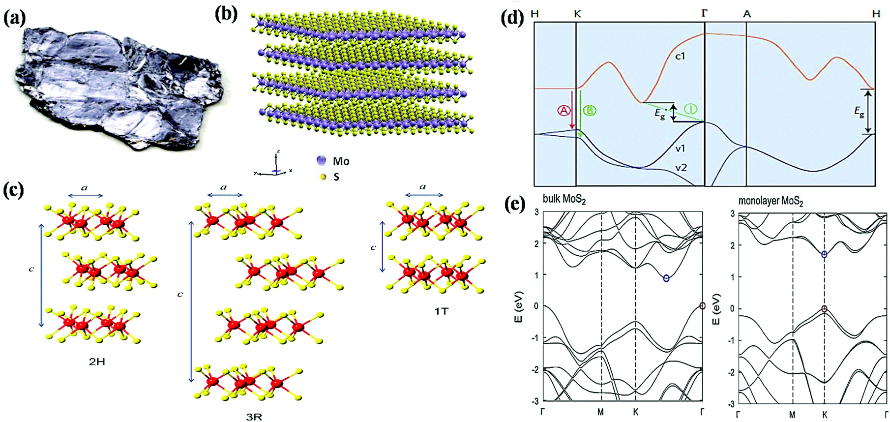 | ||
| Fig. 1 (a) Picture of bulk MoS2 crystal. Reproduced from ref. 29. (b) Three-dimensional model of the crystal structure of MoS2. Reproduced from ref. 33. (c) Schematic illustration of the various crystal structure polytypes: 2H, 3R and 1T. Reproduced from ref. 36. (d) Typical band structure of MoS2, where c1 represents the conduction band and v1 and v2 the valence bands. A and B show the direct band-gap transitions and I stands for the indirect band-gap transition. Eg and E′g represent the direct and indirect band-gap for the monolayer and bulk, respectively. Reproduced from ref. 28. (e) Illustration of the electronic band structures of bulk and monolayer MoS2. Reproduced from ref. 29. | ||
The electronic structure of semiconducting 2H-MoS2 includes its band structure and change in band structure, which are controlled by the number of layers and change in hybridization between the d orbital and Pz orbital of Mo and S, respectively.31,37 The band structure and change in band gap with respect to layer number is illustrated in Fig. 1d and e, respectively.28,29 According to the literature, bulk MoS2 possess an indirect bandgap with an energy gap of 1.2 eV, while its bandgap becomes direct for few or single-layer MoS2 with an energy gap of about 1.9 eV, which varies with the tuning of the layer of MoS2.39 From an experimental view, it has been found that few-layer MoS2 exhibits four weak humped absorption peaks in the wavelength range of 250–700 nm. Among them, the characteristic peaks observed in the range of 250–450 nm are mainly attributed to the higher excited states or bands, whereas the doublet located in the range of 600–700 nm originates from the direct excitonic transition occurring at the Brillouin zone K point between the VBM and CBM due to the spin–orbit dissociation of transition at that point.37,39 Moreover, the change in bandgap energy, i.e., from indirect to direct with a change in layer number also greatly affects the photoluminescence spectrum (PL), absorption spectrum and photoconductivity of MoS2. It has been shown that the intensity of the PL spectrum is inversely proportional to the layer number, where few-layer or thin layer MoS2 exhibits the strongest PL intensity with a large quantum efficiency. Experimentally, the two excitonic peaks in the PL spectrum of MoS2 are observed at ∼1.9 eV and ∼2.08 eV at the K point, which may be due to the spin–orbit band splitting near the valence band. It has been shown that monolayer MoS2 exhibits a main peak at 1.9 eV due to its direct gap luminescence, whereas few layer MoS2 show additional peaks together with the main peak originating from the direct gap hot luminescence and indirect-gap luminescence.37,41 Further, the valence band is derived from the overlapping of the filled dz2 orbital of Mo-4d with the filled sp orbital of the S atoms. Conversely, the conduction band is determined by the degenerate Mo-3d orbitals, i.e., dx2−y2, dz2, which overlap with the empty antibonding orbitals of the S atom.39
MoS2 has two distinctive orientations in its structure, namely basal planes with surface inertness and edge planes with high surface energy, and each orientation is terminated by chalcogen atoms. The electrical conductivity along the layer is very high, while it is low across the van der Waals gaps between the layers, which indicates that compared to the basal planes, the edge sites exhibit the fast transportation of electrons.30,42,43 Hence, in recent decades, ultrathin MoS2 has been demonstrated to be an excellent electrocatalyst towards the hydrogen evolution reaction.43,44 Moreover, its properties such as high chemical stability, superior charge carrier mobility, good surface to volume ratio and visible light absorbing property makes it an ideal candidate catalyst for photocatalytic reactions.39,45–48 More importantly, MoS2 is considered to be a good substitute for noble metals (such as Pt, Rh, Ru, and Pd) and a low-cost catalyst for both photocatalytic and electrocatalytic reactions. Although the absorbance edge of MoS2 extends from the UV-Vis to IR region, which seems ideal as a solar light harvester, single MoS2 has negligible photocatalytic activity towards energy production. This poor photocatalytic activity is attributed to the insufficient charge separation and low conductivity power between the adjacent S–Mo–S layers, which lead to poor charge mobility.49–51 Accordingly, the abovementioned difficulties have been overcome using various techniques such as sulfur edge activation, phase transition, heteroatom doping, and fabrication of heterojunction or composite with other materials. Among the various strategies, many studies reveal that the formation of hierarchical composites of MoS2 with other 2D-layered materials such as 2D-metal, 2D-semiconductor and 2D-insulator provides abundant active sites and immense surface area, which greatly enhance the effectiveness of the reaction.52–55
Although several excellent reviews summarizing the advantages, synthetic techniques, different physicochemical properties and potential application of 2D/2D heterostructures have been published, there is no comprehensive review on 2D-MoS2-based 2D/2D heterostructure materials. Therefore, herein we present an in-depth overview on the recent progress in the development of 2D MoS2-based 2D/2D heterostructure catalysts towards energy production. It includes various emerging strategies and fundamental aspects on the recent development of 2D MoS2 and its synthetic methods, photocatalytic and electrocatalytic activity, and on-demand modification of its photo/electrocatalytic activity via the introduction of other 2D materials. Subsequently, the various applications summarized in this review mainly include photocatalytic and electrocatalytic hydrogen evolution, CO2 reduction and nitrogen reduction. Therefore, in this review, we offer the latest progress in the 2D-MoS2 based 2D/2D heterostructure catalyst towards energy benefits along with various catalytic mechanisms.
2. Basis for 2D/2D heterostructures and types of interfacial coupling
2D/2D material-based composites possess a solid structure, which provides a large intimate contact interface between the individual materials, resulting in excellent photo/electro stability in the catalyst.17,56,57 Moreover, in 2D/2D heterostructures, interfacial charge migration and separation is more efficient due to the formation of a large contact area, which provides trapping channels by the large lateral size of the combined 2D materials. In the case of photocatalytic reactions, besides the formation of a high surface contact, the type and nature of the intimate interface are crucial parameters to accelerate charge carrier migration, thus suppressing the formation of photogenerated electron–hole pairs.58–63Generally, there are two directions, i.e., vertical and lateral, for the engineering of 2D/2D heterostructures with a different contact interface (Scheme 1). In the lateral direction, 2D/2D heterostructures are successfully achieved through the cross-section interface contact via the epitaxial growth method, which can be considered to be both a patterned and paralleled contact surface. In contrast, 2D/2D heterostructures in the vertical direction are realized via face-to-face contact and acquired by stacking two or multiple monolayer sheets of different nanomaterials. This method proceeds through atomic precision by regulating the relative orientation between the single 2D components.54,64–67 However, Wang et al. demonstrated a high-quality MoS2![[thin space (1/6-em)]](https://www.rsc.org/images/entities/char_2009.gif) :h-BN vertical heterostructure via a stacking process of two 2D crystals on top of each other, which provided better interlayer interaction at the interface.68 Behranginia et al. synthesized a lateral MoS2/graphene 2D/2D heterostructure, which provided a high quality lateral interface between MoS2 and graphene.69 Moreover, Yoo and coworkers reported both a lateral and vertical heteroepitaxy interface between WS2 and MoS2 monolayers by carefully controlling the contamination and defects in each 2D crystal. The as fabricated lateral and vertical 2D/2D heterostructure provides a building block for an abrupt and patterned junction in 2D materials.70
:h-BN vertical heterostructure via a stacking process of two 2D crystals on top of each other, which provided better interlayer interaction at the interface.68 Behranginia et al. synthesized a lateral MoS2/graphene 2D/2D heterostructure, which provided a high quality lateral interface between MoS2 and graphene.69 Moreover, Yoo and coworkers reported both a lateral and vertical heteroepitaxy interface between WS2 and MoS2 monolayers by carefully controlling the contamination and defects in each 2D crystal. The as fabricated lateral and vertical 2D/2D heterostructure provides a building block for an abrupt and patterned junction in 2D materials.70
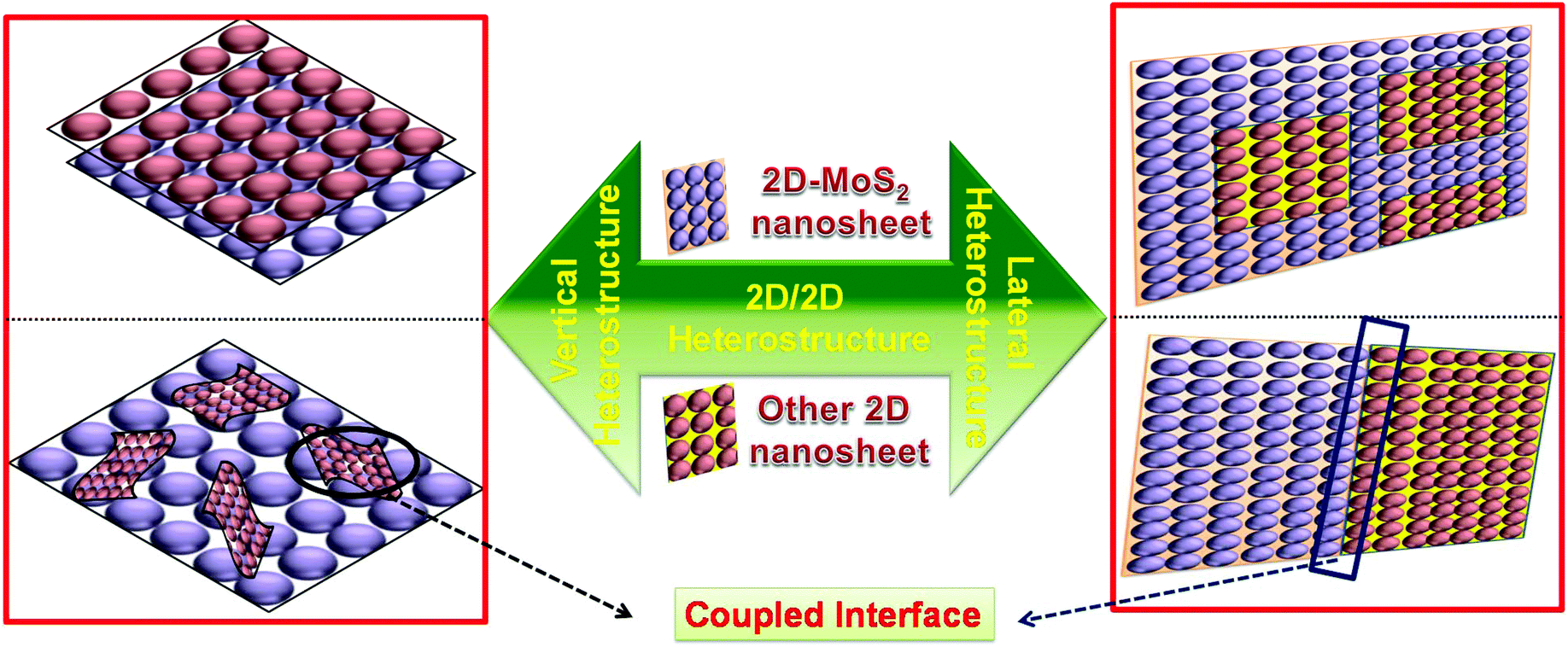 | ||
| Scheme 1 Schematic representation of the 2D/2D vertical (left) and lateral (right) heterostructures with a coupled interface. | ||
In terms of bonding, 2D/2D heterostructure including covalently bonded and van der Waals interacted heterostructures fall in a category. Considering that the layers of 2D materials are connected by via both covalent bonding (strong) and van der Waals forces (weak), during the formation of a well-defined 2D/2D heterostructure with a covalent bonding interface, it is necessary to maintain both the lattice constant matching and valence matching on each side of the interface. However, in terms of van der Waals integration, although the van der Waals forces between the layers are weak, it does not rely on either lattice matching or valence matching, but facilitates the formation of a broader heterostructure phase space, which mediates various catalytic reaction across the interface.64,66,71,72 Thus, it has been concluded that to successfully construct a 2D/2D interface, it is necessary to achieve strong interfacial bonding by optimizing the interaction forces in the composite structure. Generally, in the case of MoS2-based 2D/2D heterostructures, the strength of the interfacial bonding is regulated through various factors such as chemical bonding, Coulomb force, van der Waals force, and electrostatic interaction. For example, Yu and his group designed an MoS2/graphene 2D/2D van der Waals heterostructure with face-to-face contact through the alternating arrangement of monolayer MoS2 nanosheets and graphene. It was observed that the obtained coupled interface improved the electronic conductivity of the heterostructure material by providing more edge active sites and defects.73 Further, Shi et al. employed a simple electrostatic self-assembly process followed by the hydrothermal method to design MoS2/g-C3N4 nanosheets, which provided abundant available reaction sites for enhanced photocatalytic activities. In this case, the positively charged g-C3N4 obtained via the protonation method interacts electrostatically with the negatively charged MoS42− under hydrothermal treatment.74 In addition, each atom, i.e., Mo and S, present in MoS2 also contributed to the formation of chemical bonds during the construction of 2D/2D heterostructures. For example, Zhao et al. reported an in situ pyrolysis strategy to achieve 2D/2D MoS2/C3N4-based electrodes through Mo–N coordination between 2D-MoS2 and 2D-C3N4, which act as the main active sites for catalyzing the NRR by promoting electron transfer, thus improving the catalytic activity across the MoS2/C3N4 interface.75 In another study, Swain et al. fabricated strong interface coupling between 2D-MoS2 and 2D-CaIn2S4 through an S–S linkage, which facilitated the channelization of photogenerated charge carriers throughout the interface of both 2D materials.76 Furthermore, Wan et al. developed an Au-coupled Bi2WO6–MoS2 heterojunction photocatalyst in which the charge transfer process occurred from the surface of Bi2WO6 to MoS2via the interfacial S–O bonds. It was observed that the interfacial S–O bond is derived from the outer sulfur atoms and vertex oxygen atoms present in the MoS2 layer and WO6 octahedron of Bi2WO6, respectively.77
3. Procedures for the synthesis of 2D-MoS2 and MoS2-based 2D/2D heterojunction composites
The practical application of various 2D nanomaterials is mainly governed by their exposed active sites, and thus it is an essential requirement to design nanomaterials with properties having large area uniformity and layer controllability. Accordingly, considerable efforts have been devoted to the construction of 2D MoS2 and MoS2-based 2D/2D heterostructures with satisfactory yields, controllable thickness, unique size, and controllable morphologies by engineering synthetic techniques. The detailed procedures employed for the synthesis of 2D-MoS2 together with its 2D/2D heterostructures are depicted in Scheme 2.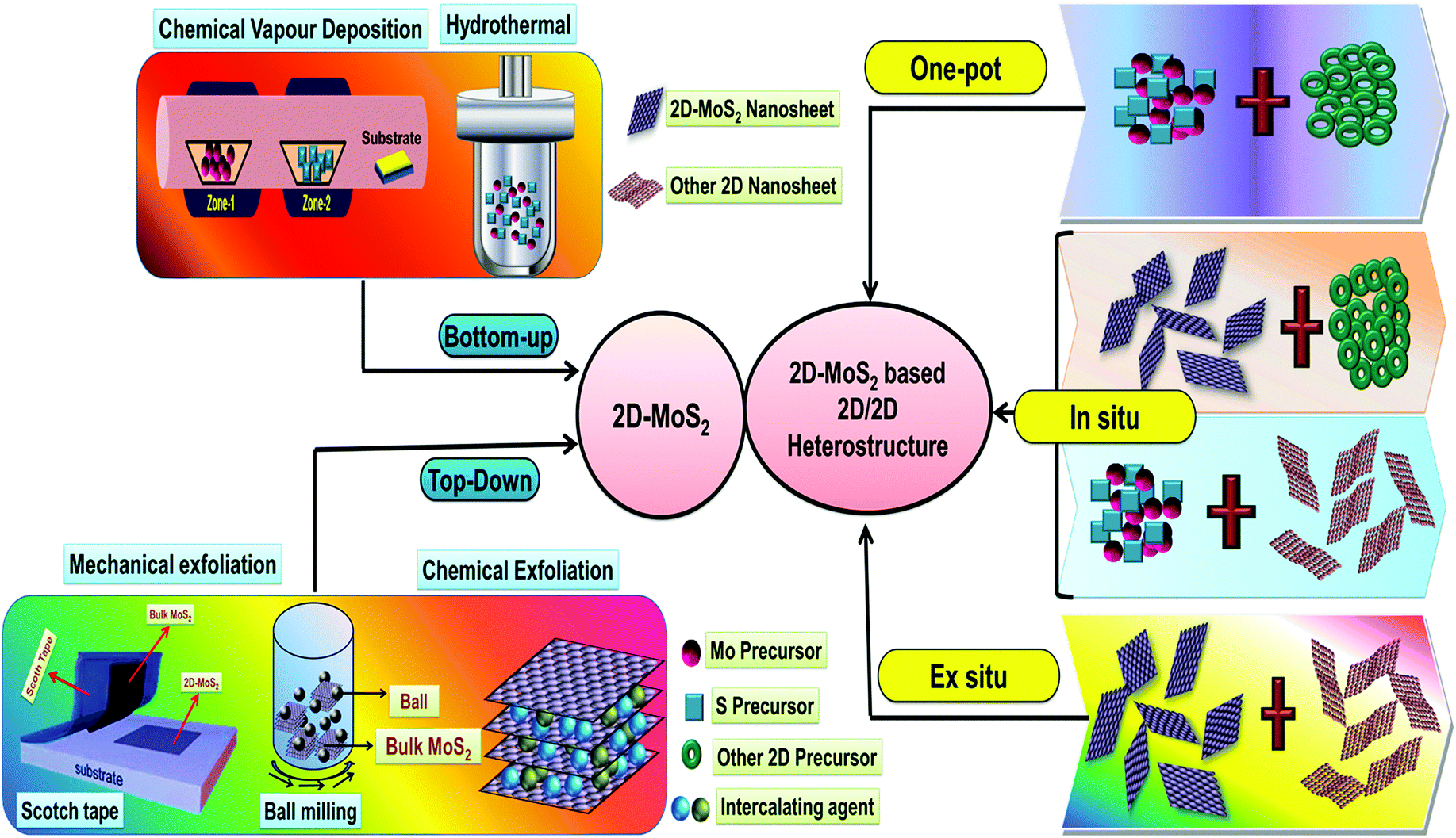 | ||
| Scheme 2 Schematic illustration of the various techniques used for the synthesis of 2D-MoS2 and its 2D/2D-heterostructures. | ||
3.1 Synthesis of 2D-MoS2
To date, numerous synthetic procedures have been developed for the synthesis of various nanostructured 2D MoS2, which can be divided into two routes, i.e., (a) top-down routes including mechanical exfoliation and chemical exfoliation and (b) bottom-up routes including hydrothermal and solvothermal method, chemical and physical vapour deposition, and decomposition method.32,393.1.1.1 Mechanical exfoliation. Similar to the Scotch tape method for the preparation of graphene from graphite, bulk MoS2 is attached on an adhesive tape and subjected to repeated exfoliation on the support of a substrate to produce a high-quality monolayer phase of MoS2. Consequently, its pristine crystal structure is the same as that of its bulk. Li and co-workers constructed MoS2 nanosheets through the mechanical exfoliation method using Al2O3 ceramic substrates.78 As illustrated in Fig. 2a, thin MoS2 flakes were obtained when the attached Scotch tape was removed from the bulk MoS2 crystals by repeatedly folding and separating the Scotch tape-adhered MoS2 flakes. Subsequently, the Scotch tape attached to the MoS2 thin flakes was tightly pasted onto a clean Al2O3 ceramic substrate on the support of Ag–Pd interdigital electrodes and left for about 6 h to maintain the adhesion state. To remove the adhesive residue from the Scotch tape, acetone was used as the solvent. The as-obtained few-layer microstructure of MoS2 exhibited a smooth surface on the substrate together with the same pattern as the substrate and it possesses the good crystallinity of MoS2 nanosheets with an ordered arrangement of lattice fringes, as presented in Fig. 2b and c. However, this process requires a substrate for sample preparation, which gives a very low product yield, and it is very difficult to control the size, shape and thickness of the resulting material. Consequently, this method is not suitable for the large-scale production of the materials. Besides the Scotch tape method, ball milling is another strategy that is also responsible for the synthesis of high-quality 2D MoS2 nanosheets. Krishnamoorthy et al. mechanically delaminated bulk MoS2 into few-layered MoS2 nanosheets using the ball milling method. The ball milling method is performed in a ball and bowl made up of tungsten carbide, and N-methyl-2-pyrrolidine (NMP) is used as the solvent throughout the reaction. After ball milling at a speed of 300 rpm, the final MoS2 product is obtained after washing with ethanol followed by drying.79 Besides the Scotch tape and ball milling techniques, in 2012, Gacem's group reported an anodic bonding technique, in which high-quality nanosheets with high yield, good optical properties and excellent purity were obtained.80
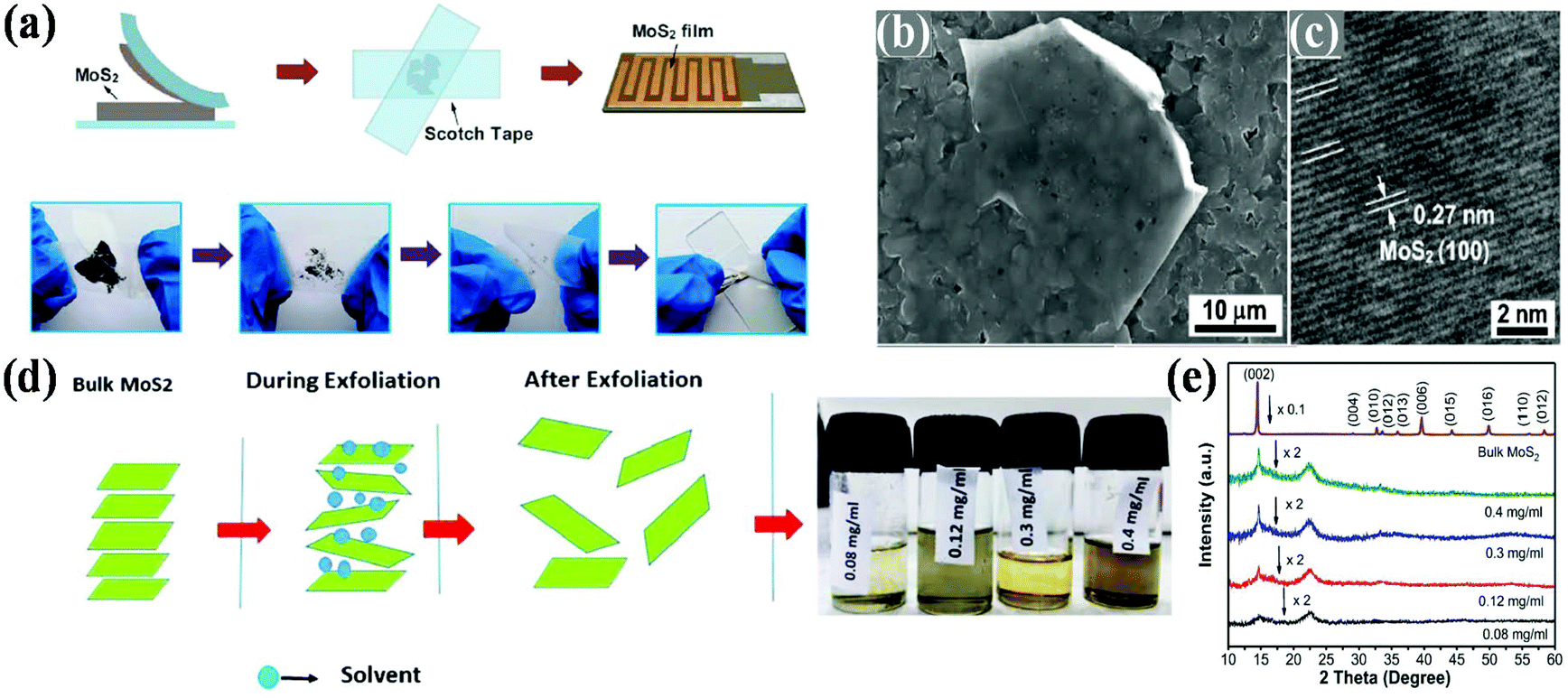 | ||
| Fig. 2 (a) Schematic diagram showing the mechanical exfoliation technique for the synthesis of MoS2 nanosheets, and (b) SEM and (c) HRTEM images of MoS2 nanosheets. Reproduced from ref. 78 (d) Scheme of the synthesis process via the liquid-phase exfoliation of MoS2 nanosheets and (e) X-ray diffraction patterns of bulk MoS2 powder and MoS2 nanosheets synthesized using different initial concentrations of bulk MoS2. Reproduced from ref. 81. | ||
3.1.1.2 Liquid-phase exfoliation. In this method, few-layered materials are prepared directly under the influence of various solvents followed by the joint action of sonication and centrifugation. Here, sonication breaks the weak van der Waals interaction present between the stacking layers without destroying the covalent bonding in each layer.38 This technique includes ion intercalation, ion exchange and ultrasonic cleavage, which generates a large amount of 2D-MoS2 with good quality single and few-layered nanosheets. The choice of solvent is a key parameter in liquid exfoliation, where there should be a good match between the solvent and surface tension present between the layers, which minimizes the energy required for exfoliation, thus increasing the exfoliation efficiency. Here, the number of layers in the resulting 2D materials is governed by the choice of solvent together with the concentration of the precursor solute. Gupta and co-workers prepared MoS2 nanosheets through the liquid-phase exfoliation method using NMP as the exfoliating solvent. From experimental studies, it has been deduced that the presence of a small mole fraction of water in NMP stabilizes the MoS2 nanosheets in the dispersion during sonication. Particularly, the stability of the MoS2 nanosheets in the NMP dispersion solution is due to the water molecules confined at the Mo edges of MoS2, which prevent chemical erosion of the edges. This, enhances the interaction between the NMP solvent and MoS2, leading to a stable dispersion.82 Therefore, it has been concluded that the use of solvent during the exfoliation method is not only responsible for the synthesis of two-dimensional nanosheets, but also plays a big role in stabilizing the nanosheets. In the literature on studies regarding liquid-phase exfoliation, it has also been observed that solvents with a low volatile rate hamper the rate of exfoliation and yield of 2D catalysts. Thus, the choice of solvent with a high volatility rate is another crucial factor that should be considered. Accordingly, Sahoo et al. employed a cost-effective liquid-phase exfoliation route for the scalable production of high-quality MoS2 nanosheets using acetone as the solvent. The use of acetone as a solvent overcomes the drawbacks of low-volatility solvents. In this method, the bulk MoS2 is exfoliated into 2D-MoS2 nanosheets via sonication followed by centrifugation. The synthetic method involves several steps as follows: (i) grinding of bulk MoS2 using a mortar and pestle followed by drying to evaporate the water and impurities, (ii) addition of acetone to a particular concentration of dried MoS2 in a glass vial, (iii) treatment in a sonication bath to interrupt the weak van der Waals force present between the adjacent layers, and (iv) finally the supernatant is collected using a micropipette after centrifugation followed by filtration. Fig. 2d depicts the procedure for the synthesis of MoS2 nanosheets via the weakening of van der Waals forces, which helps in thinning the layers, where the exfoliation procedure proceeds with different initial concentrations. As shown in Fig. 2e, the strong diffraction peak observed at the (002) plane decreases gradually with a change in the initial concentration of bulk MoS2 in a given concentration of solvent, indicating that the bulk MoS2 is exfoliated to few layers. Moreover, in the case of the ion intercalation mechanism, cations are intercalated into the interlayer spacing of the bulk materials to destroy the van der Waals interaction present between the layers.81 However, the use of harmful toxic organic solvents, low quantum yield, and small lateral size of the as-obtained sheets limit its large scale utilization by many researchers.
3.1.2.1 Chemical vapour deposition. The chemical vapour deposition (CVD) approach involves the growth mechanism of the products via chemical reactions and has been proven to be a beneficial method to synthesize high-quality substances that are thin and highly conductive, especially MoS2 films. The CVD method requires a two-furnace approach to control the temperature of both Mo and S precursors separately. In a typical process, the desired product is obtained due to the redox reaction between the reactant precursors on the support or surface of a substrate whenever one or more volatile precursors decompose and react with each other at high temperature and high vacuum conditions. Typically, the growth temperature is maintained about 700–1000 °C and for the growth of 2D-MoS2 thin layers, various substrates are employed as insulating supports. Initially, the MoS2 precursors such as Mo, MoO3, (NH4)2MoS4 are deposited on the supporting surface and then subjected to thermal decomposition or sulfurization at an elevated temperature to generate MoS2 layers with controlled structures.37,46,83
In addition, by customizing the essential parameters (growth temperature and time, flow rate of the carrier gas, mass amount, and the position of both the reactant and substrate), a high-quality MoS2 monolayer can be achieved together with tunable film thickness and large active sites, which are beneficial for interplanar charge transport. Wan and his group demonstrated fractal-shaped single-layer MoS2 to engineer the active sites of MoS2 through the CVD method on a fused silica substrate. It was observed that water-soluble polymer-assisted method prevented the formation of the fractal-shaped morphology during the transformation process.84 Li and co-workers employed a single-step CVD approach (Fig. 3a) for the development of an edge-enriched 2D-MoS2 thin film with high catalytic efficiency towards the HER. The CVD process was carried out on a wide range of substrates including a silicon wafer, graphite, and glassy carbon. During the synthesis, the total number of edge sites on MoS2 and its surface area increased when smaller layered MoS2 grew on large MoS2 platelets in a perpendicular direction (Fig. 3b). The TEM images in Fig. 3c and d demonstrate the formation of vertically orientated layers, in which vertically aligned nanoflakes are grown on the petal site of MoS2.85
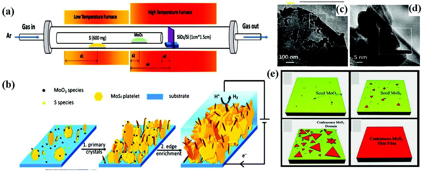 | ||
| Fig. 3 (a) Schematic representation showing the experimental CVD setup, (b) mechanistic demonstration of the edge enrichment of MoS2, (c) and (d) TEM images of the petal site showing the nucleation of vertically aligned nanoflakes on the top-layer crystals. Reproduced from ref. 85. (e) Schematic illustration of monolayer MoS2 growth on a Piranha-treated substrate. Reproduced from ref. 86. | ||
In terms of wafer-scale production with low manufacturing cost and highly crystalline MoS2, the atmospheric pressure chemical vapour deposition (APCVD) method has emerged as an excellent approach. Gnanasekar and his group developed a high-quality MoS2 monolayer for the electrochemical hydrogen evolution reaction using a seed promoter-free APCVD method directly on an SiO2 substrate. The CVD method mainly involves the transport and adsorption of the final growth species on a given substrate followed by the nucleation and future growth of new MoS2. Initially, at a particular high temperature, the Mo precursors are reduced and are adsorbed on the arbitrary position of the substrate with the flow of carrier gas, which is further subjected to a sulfurization process, resulting in nucleated species. The as-obtained MoS2 acts as a seed, which allows further growth of another MoS2 thin film. The overall reaction procedure is depicted in Fig. 3e. From the experiment, the large scale high-quality MoS2 possessed excellent HER properties.86 However, using this method, it is very challenging to prepare MoS2 crystals by controlling the number of layers due to the use of non-crystalline precursors, where it is difficult to control the number of layers of the product material during the reaction.
3.1.2.2 Hydrothermal or solvothermal method. Among the various synthetic methods, the hydrothermal process is preferred by many researchers because it can achieve high surface area, good-quality crystals and controlled morphological composition of the products. It is a growth method in which water and organic and inorganic solvents are used as the reaction medium dissolve the commonly used Mo and S precursor substances. The reaction generally involves the crystallization of a material under high pressure (1 MPa to 1 GPa) and high temperature (100–250 °C) conditions from an aqueous and organic solvent. This technique is very promising due to its safe and simple operation, mild conditions, high purity, low pollution, low cost and easy hybrid dispersion nature. The solvothermal synthesis technique of 2D-MoS2 basically requires the use of an organic/inorganic sulfur source such as thioacetamide, thiourea and KSCN, and sodium molybdate, ammonium molybdate, and molybdenum trioxide as the Mo source. By controlling the reaction temperature and time, the size, crystallinity and morphology of the resultant 2D-MoS2 can be modulated to some extent.34,37,87 Muralikrishna and co-workers synthesized 2D MoS2 nanosheets with high catalytic activity via a facile hydrothermal approach, which exhibited superior electrocatalytic HER activity.88 The sulfur source used was thiourea, which acts as both a reducing agent and stabilizer, which stabilizes the defect-rich MoS2 nanosheets. Under hydrothermal conditions, i.e., high temperature and high pressure, firstly Mo(VI) present in MoO3 is reduced to Mo(IV) under the influence of excess thiourea. Finally, the reduced Mo(IV) couples with the excess thiourea and undergoes a nucleation process and is converted to MoS2 nanoparticles, which then grow into defect-rich nanosheets. The use of ammonia during the reaction procedure has a great advantage over the stacking of MoS2 nanosheets and facilitates the production of thin nanosheets very easily. In another study, Swain et al. prepared crumpled-type exfoliated MoS2 nanosheets under simple one-step hydrothermal conditions. It was also observed that without the inclusion of any surfactants, the hydrothermal technique is also responsible for the production of highly efficient morphological-oriented structured MoS2 nanosheets.89 In this regard, Swain et al. designed rose-like MoS2 nanoflowers by employing a facile hydrothermal technique using only water as the solvent. The as-obtained MoS2 exhibited like a rose-like nanoflower structure with a diameter of 500–800 nm. During hydrothermal treatment from the precursor salt solutions of Mo and S, firstly the MoS2 nanoparticles self-aggregate and undergo a reduction in surface energy and get converted into partially monodispersed isolated MoS2 microspheres. Under a prolonged hydrothermal process with an increase in temperature, petal-like nanosheets of MoS2 are grown on the surface of the MoS2 spheres, thus displaying a hierarchical rose-like MoS2 nanoflower morphology.90 Several studies have also reported that the introduction of the combined effect of both defects and S-vacancy results in superior catalytic activity. Li et al. employed a facile hydrothermal method for the synthesis of multilayered MoS2 nanosheets in N,N-DMF using (NH4)2MoS4 as both the Mo and S precursors. The as-obtained MoS2 consisted of point-defect S-vacancies together with coordinated Mo regions, which reduced the free energy of hydrogen adsorption during the HER.91
3.2 Techniques for the synthesis of MoS2-based 2D/2D heterostructures
The fabrication of MoS2-based 2D/2D heterostructure composites with controllable nanostructured properties is a great challenge in the current research scenario. The techniques for the synthesis of MoS2-based 2D/2D heterostructures are broadly categorized into two classes: (a) ex situ synthesis method and (b) in situ and one-pot synthesis method.53,65 Among the various reports in the literature, only a few are discussed in the following section.It should be noted that in some cases, a single 2D material can be directly exfoliated from its bulk under the action of some solvent and exfoliation treatment, whereas in some cases, the neat material can be prepared from its molecular precursors directly. For example, Xiong et al. fabricated a 2D/2D MoS2/CdS heterojunction by employing an adsorption–calcination process, as shown in Fig. 4a. This method involved the preparation of neat 2D-MoS2 from its commercial bulk counterpart through exfoliation, whereas neat CdS was prepared through the solvothermal–precipitation route followed by exfoliation to get an ultrathin nanosheet structure. Then, the two above-prepared neat materials were mixed through the adsorption process via sonication, and then further subjected to a calcination process (Ar atmosphere), which facilitates the close contact between the two components.92 Similarly, Jeong et al. fabricated a black phosphorus (BP)@MoS2 2D/2D nanocomposite by mixing as-exfoliated BP and MoS2 through the ball milling method followed by high energy ultrasonication.93 Meanwhile, another type of 2D/2D nanojunction was constructed through the direct assembly strategy followed by the reflux method, in which MoS2 nanosheets with 6 to 8 layers were prepared through a simple solvothermal method followed by exfoliation strategy, whereas Bi2WO6 nanosheets were prepared through a hydrothermal method, which were then dispersed in NMP (N-methyl-2-pyrrolidone) solvent via sonication followed by reflux. The large and close 2D/2D contact surface of the Bi2WO6/MoS2 heterojunction is favorable for interfacial charge transfer. In heterojunction materials, the abundant reductive active sites and high electron conductivity are mainly dependent on the controlled S–Mo–S layer of MoS2 nanosheets, which look like curled edges. It was observed that the controlled curled edges of MoS2 possess a larger interlayer spacing (0.702 nm and 0.685 nm) compared to that of bulk MoS2 (0.61 nm).77
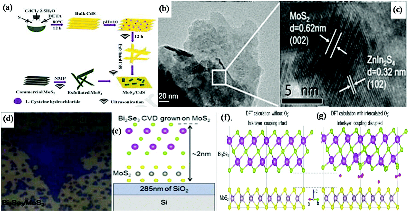 | ||
| Fig. 4 (a) Strategy for the fabrication of MoS2/CdS heterojunctions. Reproduced with permission.92 (b) SEM and (c) HRTEM images of ZnIn2S4/MoS2 composite. Reproduced with permission.95 (d) Optical image and (e) side-view diagram of Bi2Se3/MoS2 heterostructure, (f) charge redistribution representation of the interlayer region and the interlayer coupling and (g) interlayer coupling with interlayer separation by O2 molecule of Bi2Se3/MoS2. Reproduced with permission.96 | ||
In addition, ex situ strategies are also regulated through ball milling and the mechanical grinding method. Li et al. developed a 2D/2D C3N4/MoS2 heterojunction photocatalyst with a stable intrinsic crystal structure via a simple mechanical grinding method. They mixed an appropriate amount of commercial MoS2 and g-C3N4 and put it on ball grinder for mechanical operation.94 However, good interfacial contact was also achieved through the electrostatic self-assembly approach, considering the zeta potential value of each neat material. By following this strategy, Huang et al. designed a sheet-on-sheet 2D/2D ZnIn2S4/MoS2 heterostructure, in which MoS2 nanosheets were well connected with ultrathin sheets of ZnIn2S4. Briefly, initially, both pristine materials have negatively charged surfaces with a zeta potential value of −23.8 mV and −45.7 mV for the MoS2 and ZnIn2S4 nanosheets, respectively. However, after treatment with poly(diallyldimethylammonium chloride) (PDDA), the negative surface of the MoS2 nanosheets in the aqueous dispersion changed became positive with a zeta potential value of +36.5 mV. After the modification, strong electrostatic attraction occurred between the negatively charged ZnIn2S4 and positively charged PDDA-MoS2, which provided the necessary condition for the development of a 2D/2D heterostructure with an intimate contact interface for efficient charge separation and migration. The sheet-on-sheet structure with large contact interface and individual clear fringes for neat MoS2 and neat ZnIn2S4 in the 2D/2D ZnIn2S4/MoS2 heterostructure is presented in Fig. 4b and c, respectively.95
Besides the above-mentioned methods, the transfer process in which a single 2D material originates from the CVD method is also treated as an ex situ method for the direct configuration of 2D/2D van der Waals heterostructures. Wang et al. developed a method for the direct growth of MoS2 on h-BN by employing an ex situ path. The MoS2/h-BN van der Waals heterostructure was prepared through a two-step poly(methyl methacrylate) (PMMA)-assisted transfer approach. The method involved the direct transfer of CVD-grown MoS2 to a new SiO2/Si substrate containing h-BN to achieve a 2D/2D heterostructure.68 It was noted that for the synthesis of more active 2D/2D van der Waals heterostructures, parameters such as the interlayer separation distance and stacking lattice orientation should be optimized. Therefore, Hennighausen et al. tuned the interlayer through the intercalation and deintercalation of diffusive atmospheric oxygen molecules. By regulating the atmospheric oxygen, the interlayer coupling in the 2D/2D Bi2Se3 heterostructure could be reduced under laser or thermal energy. The synthetic method involved the initial growth of an MoS2 monolayer followed by the growth of Bi2Se3 on top of it through vapour phase chalcogenization and vapour phase deposition, respectively. The successful uniform and regular growth of one layer of Bi2Se3 on one layer of MoS2 crystal on SiO2 and the strong van der Waals epitaxial structure were clearly observed from the optical image (Fig. 4d) and side-view diagram (Fig. 4e), respectively. The DFT calculation, as shown in Fig. 4f and g, predicted the uniform charge redistribution in the interlayer region. The relatively small-sized O2 molecules are easily intercalated in the interlayer region, as predicted by DFT calculation (Fig. 4g), which facilitates charge separation by tuning the interlayer coupling, thus making the material electronically independent.96 Subsequently, Biroju and coworkers accomplished the synthesis of sequentially stacked atomic layers throughout the development of an MoS2/graphene van der Waals solid through the wet transfer CVD method. In this case, a single layer of graphene was grown on three-four atomic layers of MoS2 by mixing and matching various layers, resulting in a transparent flexible electrode, and its efficacy in the HER was demonstrated.97
For the CVD technique, a substrate and a volatile substance are required, in which one pre-synthesized 2D material is employed as the 2D substrate on which the volatile substances are exposed so that the other 2D materials can easily react or decompose for the growth of 2D/2D heterostructures. When the reaction is complete, volatile byproducts are produced, which are removed from the reaction system with the help of a gas flow. This is the most promising technique for the synthesis of hybrid materials based on the 2D/2D architecture.53,65 Moreover, it has been observed that during the growth process, given that the precursors of both 2D materials coexist in the vapor phase, there may be a cross-contamination issue with the various elements present in the as-fabricated 2D/2D heterostructure. However, this issue can be mitigated through the two-step CVD growth strategy, in which two 2D composite layers are synthesized in two separate steps and the growth process on a metal substrate is found to be more effective. This method offers high-quality 2D/2D TMD heterostructures together with a pure phase, resulting in versatile applications in various fields.
Zhai et al. developed 2D-van der Waals heterostructures using NiTe2/MoS2 through a two-step in situ CVD growth method. The as-fabricated heterostructure possessed a better heterointerface and enhanced electronic and optoelectronic performances, which were found to be three orders greater compared to that of single 2D-MoS2. The epitaxial growth of the van der Waals heterostructure is mainly attributed to the similar hexagonal symmetry of both 2D layered materials. In this case, firstly, by using the low-pressure chemical vapour deposition (LPCVD) strategy, MoS2 monolayers are grown on SiO2/Si substrates. It should be noted that the LPCVD method is easier and much more beneficial for designing high crystalline monolayer MoS2 with a clean and triangular surface. After the formation of triangular MoS2, it is employed as a substrate for the growth of an NiTe2 layer, resulting in an NiTe2/MoS2 van der Waals heterostructure, in which the bottom MoS2 layer and upper NiTe2 thin film layer are vertically stacked with each other through weak van der Waals forces (Fig. 5a). Fig. 5b depicts the two-step CVD growth procedure for the synthesis of the MoS2/MoTe2 heterostructure. The vertical heterostructure of NiTe2 on the monolayer of MoS2 is depicted in the SEM image in Fig. 5c. According to the AFM image (Fig. 5d), the thickness of the upper NiTe2 and bottom MoS2 is 5.20 nm and 0.85 nm, suggesting the formation of five and single triple-layers comprised of NiTe2 and MoS2, respectively.98
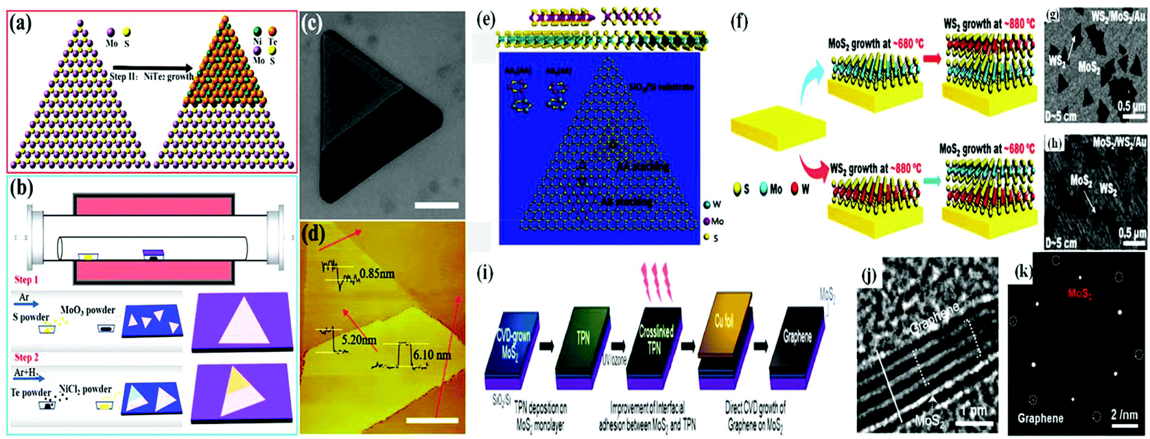 | ||
| Fig. 5 (a) Schematic illustration of the vertical stack and (b) two-step CVD growth process for NiTe2/MoS2 heterostructure. (c) SEM image depicting the vertical heterostructure of NiTe2/MoS2 on an SiO2/Si substrate. (d) AFM images of vertical stacking region and interfacial region. Reproduced with permission.98 (e) Atomic representation of vertically assembled A–A and A–B stacked (top and side views) MoS2/WS2 bilayers. Reproduced with permission.99 (f) Schematic diagram representing the two-step CVD growth process. (g) and (h) SEM images of WS2/MoS2/Au and MoS2/WS2/Au, respectively. Reproduced with permission.100 (i) Schematic representation showing the direct growth of graphene/MoS2 heterostructure on SiO2/Si substrate, (j) HRTEM image of graphene/MoS2 heterostructure and (k) SAED image of MoS2 monolayer (red circle) and graphene (white circle). Reproduced with permission.101 | ||
Furthermore, it has been demonstrated that vertical bilayers with the strongest interlayer coupling and shortest interlayer spacing can be obtained based on the twisted stacking angles with equivalent crystallographic alignment in van der Waals heterostructures, such as A–A or A–B-type stacking. Due to this type of modulation in the interlayer coupling, the heterostructure exhibits superior optical and electrical properties, i.e., it facilitates the interlayer transfer and migration of charge pairs, thus reducing the charge recombination more efficiently. Zhang et al. reported the epitaxial growth of an MoS2/WS2 heterostructure, in which MoS2 films were grown on top of WS2 through a two-step CVD growth approach in the A–A and A–B stacking fashion. The top and side atomistic views of the heterostructure are presented in Fig. 5e. In this case, MoS2 is nucleated at the edges of WS2 in a triangular shape with only 0° and 60° orientations with respect to the bottom WS2 layer, maintaining the most stable A–A and A–B stacking configurations, respectively. According to the Raman spectra study, the A–B stacked bilayers had a strong lower breathing frequency mode than the A–A stacked bilayers, which possessed a shorter interlayer distance and stronger interlayer coupling.99
Further, Shi and co-workers designed a vertically stacked van der Waals heterostructure via the temperature-mediated selective growth of 2D-MoS2 on 2D-WS2 and vice versa using Au foil as the substrate material in the two-step CVD method.100 Briefly, as shown in Fig. 5f, in the first step, the individual monolayer MoS2 or WS2 was grown on Au foil from its precursor element (MoO3 or WO3, respectively) under a low-pressure CVD method. In the second step, the as-prepared MoS2/Au or WS2/Au samples were subjected to further heat treatment in a furnace in the presence of the corresponding metal precursors for the subsequent preparation of the 2D/2D MoS2/WS2 heterostructure. The uniform distribution and vertical growth of MoS2 or WS2 (triangular domain) on WS2/Au or MoS2/Au were clearly observed from the SEM images (Fig. 5g and h), respectively. In contrast, Lee et al. proposed a novel method for the direct growth of MoS2/graphene using the CVD technique in the presence of a UV/ozone-treated solid C-source, as illustrated in Fig. 5i. MoO3 and sulfur powder were used as the MoS2 precursors, while for the growth of graphene, 1,2,3,4-tetraphenylnaphthalene (TPN) was used as the precursor. Firstly, an MoS2 monolayer was prepared using the molten-salt-assisted CVD method, resulting in the formation of an MoS2/SiO2/Si substrate, on which the graphene layer was grown. However, UV/ozone treatment of the spin-coated TPN on MoS2/SiO2/Si substrate increased the interfacial adhesion between the two layers, and the final growth of graphene occurred under Cu vapor when Cu foil was placed on the TPN-coated MoS2/SiO2/Si substrate, resulting in the formation of the graphene/MoS2 heterostructure. The successful growth of graphene layers on the monolayer MoS2 and sharp interface between graphene and MoS2 were confirmed from the cross-sectional TEM image (Fig. 5j). Furthermore, the SAED pattern (Fig. 5k) confirmed the clean diffraction spots for both MoS2 and graphene in the graphene/MoS2 heterostructure, suggesting that the 2D/2D heterostructure is suitable for application in an ultrathin electronic device with high surface-sensitive properties.101
Besides the CVD method, the in situ process for the synthesis of 2D/2D heterostructures can also be mediated through the hydrothermal technique. Ji et al. modified 2D-CeO2 on 2D-MoS2 nanosheets through an in situ facile hydrothermal technique to design a new 2D/2D MoS2/CeO2 heterojunction, which possessed abundant reactive centers for degradation reactions.102 Throughout the reaction, the Ce4+ ions from 2D-CeO2 generated sufficient oxygen vacancies by utilizing photoexcited charge carriers and acted as redox centers. In this case, firstly, 2D CeO2 nanosheets were prepared via the hydrothermal method followed by calcination, and then introduced to the Mo and S precursors through the hydrothermal process, resulting in the formation of 2D/2D MoS2/CeO2. The morphological characterization via TEM and HRTEM of 2D/2D MoS2/CeO2 indicated that both 2D nanosheets were uniformly combined, in which the 2D-CeO2 nanosheets were located on the 2D-MoS2 nanosheets in a vertical and lateral fashion. Furthermore, Yuan et al. developed face-to-face 2D/2D black phosphorus (BP)/MoS2 through the solvothermal method, in which MoS2 nanosheets were homogeneously dispersed on the surface of BP nanosheets. It was observed that the interaction occurred between the precursors of MoS2 and the oxygen present in the exfoliated BP nanosheets, which exhibited a large intimate contact interface and abundant exposed edges for superior catalytic activity.103
Besides the face-to-face heterostructure, the in situ synthesis method is also responsible for the formation of highly efficient 2D/2D heterostructure materials with electrostatic interaction between them. By combining electrostatic self-assembly chemistry with the in situ hydrothermal strategy, Nayak et al. constructed an MoS2/Ni–Fe LDH nanocomposite.104 Particularly, 2D-MoS2 nanosheets underwent a nucleation and growth process on the edge-shared MO6 octahedron site (positively charged surface) provided by 2D-LDH, resulting in the formation of 2D/2D MoS2/Ni–Fe LDH. The overall growth process is governed through the electrostatic self-assembly and O2 vacancies in the LDH nanosheets, which effectively co-ordinate with the Mo4+ and S2− ions during the in situ hydrothermal reaction. Interestingly, both the exfoliation of strongly bonded positive layers of LDH and the growth of MoS2 nanosheets on the positively charged surface of the exfoliated LDH take place in one step during the hydrothermal reaction. Swain et al. developed a hierarchical structure with a 2D/2D contact heterojunction in which the crumpled sheets of MgIn2S4 flowers were covered with petal-like MoS2 nanosheets through S–S linkages at the interface.90 As illustrated in Fig. 6a, under hydrothermal treatment, the MoS2 nanopetals derived from the MoS2 nanoflowers under ultrasonication mixed with the precursor salt solution (Mg, In, and S) of MgIn2S4, resulting in the formation of an MoS2/MgIn2S4 marigold flower-like morphology. The resulting 2D/2D heterojunction is constructed in such a way that both neat counterparts are tightly joined with each other in a zigzag face-to-face and face-to-edge contact, providing a large number of exposed unsaturated S active sites for the photocatalytic reaction. The TEM images (Fig. 6b and c) of the MoS2/MgIn2S4 heterojunction indicate the wrapping of MoS2 nanosheets around the micro-sized petals of the MgIn2S4 flowers.
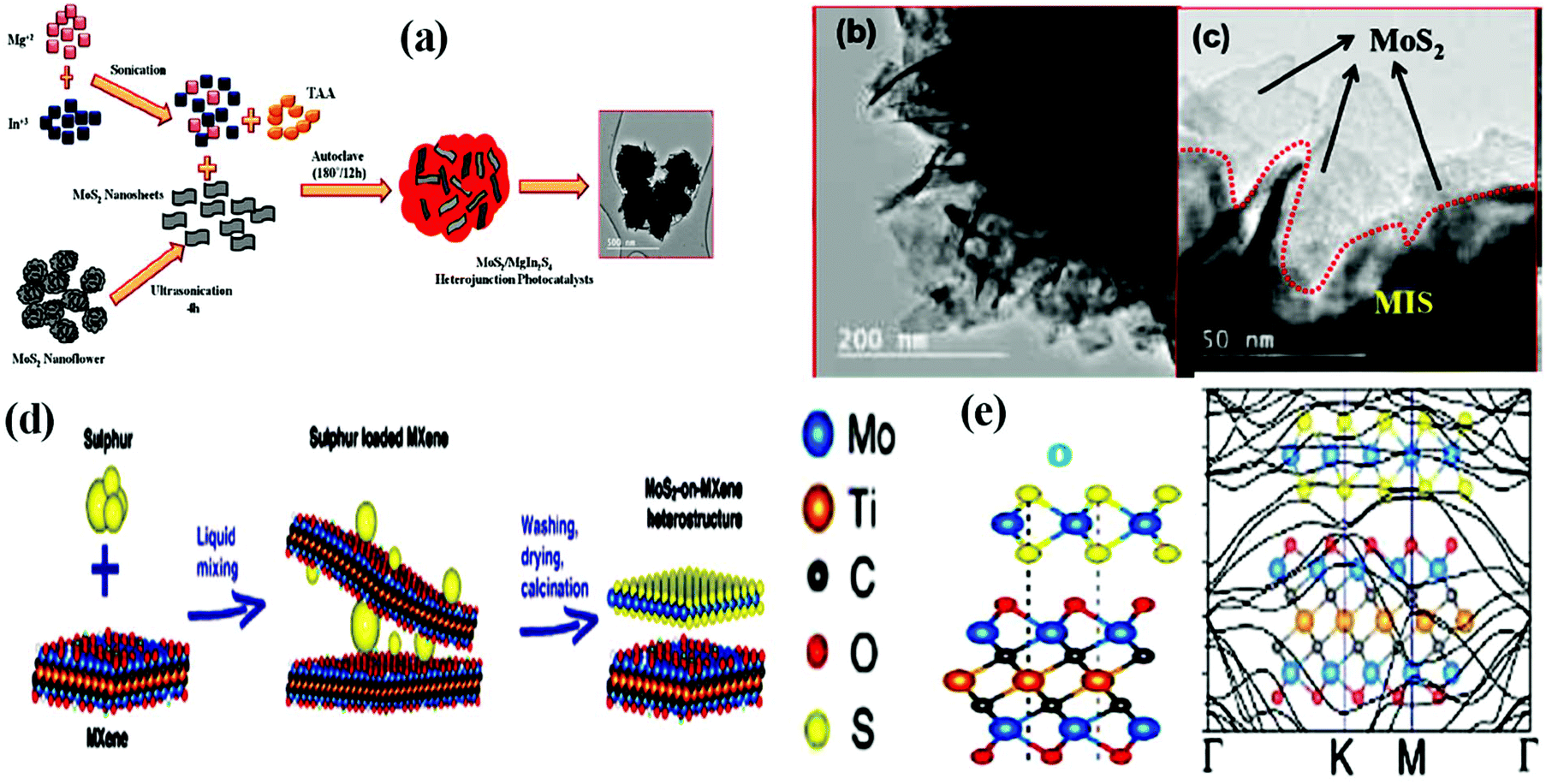 | ||
| Fig. 6 (a) Schematic diagram showing the growth mechanism and (b) and (c) corresponding HRTEM images of MoS2/MgIn2S4 heterojunction photocatalyst. Reproduced with permission.90 (d) Schematic representation of the fabrication of MoS2/MXene hybrids and (e) structural stacking patterns and electronic band structure of MoS2/Mo2TiC2O2. Reproduced with permission.105 | ||
Furthermore, highly active MoS2-based 2D/2D heterostructures can also be achieved via the partial replacement of S in 2D-MoS2 with another anion such as phosphide and carbide having a similar atomic radius or the addition of S to another non-MoS2-based material.105 2D MoP/MoS2 heterostructure nanosheets were constructed by Wu and coworkers, in which the S present in MoS2 underwent rational substitution with P. Typically, MoS2 nanosheets were evenly distributed and grown on CC cloth under hydrothermal treatment, and then MoP was obtained on the MoS2 nanosheet template under phosphorization treatment. However, the partial replacement of S with P should be controllable so that a part of the MoS2 phase remains in the final product to maintain the 2D/2D MoP/MoS2 sheet-like heterostructure. It was demonstrated that the as-fabricated 2D/2D heterostructure possessed rich active sites and good conductivity.106 In another study, Chen et al. designed a 2D MoS2-on-MXene heterostructure via the in situ sulfidation of a molybdenum-containing 2D-Mxene (Mo2TiC2Tx) material (Fig. 6d). In the Mo2TiC2Tx structure, one layer of Mo atoms is present on the surface of the Mo2TiC2Tx MXene, and thus a part of the surface Mo–O pattern can be controllably transformed into an Mo–S motif on the MXene surface under in situ sulfidation, resulting in the formation of an MoS2/Mo2TiC2Tx heterostructure with intimate interfacial interactions. The schematic mechanism suggests that under the liquid mixing process, sulfur-incorporated MXene layers are initially derived, which are further subjected to heating in an inert atmosphere, producing the final product followed by the transformation of Mo–O to Mo–S and removal of residual S simultaneously. The stable structural and electronic properties of the resulting heterostructure were depicted from the computational investigation, as shown in Fig. 6e. According to the position of the Mo and S atoms in MoS2 with respect to O and Ti in Mo2TiC2O2, respectively, it was deduced that the integration between MoS2 and Mo2TiC2O2 resulted in enhanced conductivity, which is suitable for application in Li-ion batteries.105
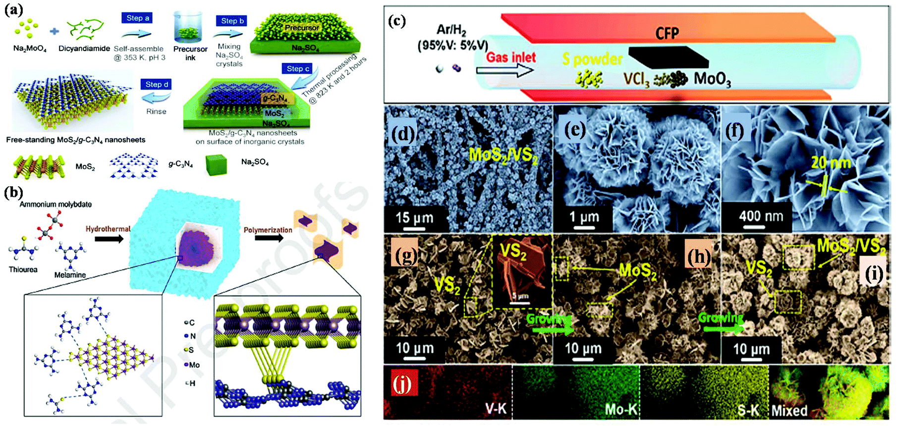 | ||
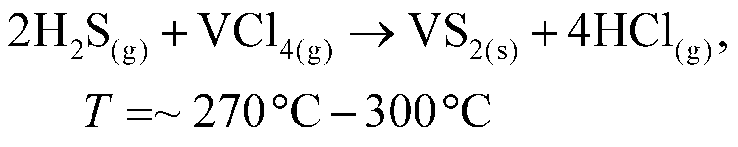
| Fig. 7 (a) Schematic illustration of the synthetic strategy for free-standing MoS2/g-C3N4 vdW layers. Reproduced with permission.109 (b) Schematic representation of the synthesis of MCN nanocomposites via the hydrothermal-polymerization method. Reproduced with permission.110 (c) Schematic diagram representing the one-pot CVD process for the preparation of the MoS2/VS2 hybrid, (d–f) SEM images at different magnifications observed for MoS2/VS2 hybrid, (g–i) TEM images of the MoS2/VS2 hybrid at different temperatures and (j) EDX colour elemental mapping of the MoS2/VS2 hybrid. Reproduced with permission.111 | ||
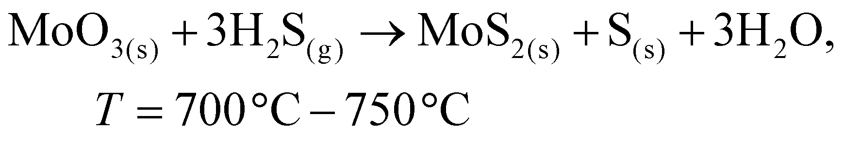
To date, the exploration of the one-pot CVD process for the controlled synthesis of 2D/2D hybrid materials has rarely been discussed although this method is very scalable, versatile and time-saving. In the literature, only a few works have been reported on the one-pot CVD method towards the synthesis of hybrid materials. Yu and co-workers proposed a one-pot CVD strategy for the successful fabrication of MoS2 microflowers on VS2 microflakes by using suitable precursors on macroporous carbon fiber paper as the substrate under atmospheric pressure, and the reaction was performed in a one-temperature-zone furnace.111 The procedure for the fabrication of the MoS2/VS2 hybrid is schematically illustrated in Fig. 7c. Typically, the metal precursors are positioned side-by-side, whereas the S element is placed at an upstream position in the quartz boat together with CFP in the middle of the furnace. The uniform growth of the MoS2/VS2 hybrids on the CFP was achieved by increasing the temperature to 800 °C under the flow of a gas mixture. The SEM images of the MoS2/VS2 hybrid at different magnifications (Fig. 7d–f) demonstrated the uniform distribution and full coverage of MoS2 on the VS2 microflakes. By modulating the temperature from low to high, they predicted that the VS2 nanoflakes are derived initially at a lower temperature, and later with an increase in the reaction temperature (high temperature), MoS2 microflowers grow on VS2. Fig. 7g–i illustrate the morphological evolution of the MoS2/VS2 hybrid at different temperatures. Depending on the temperature, four primary chemical reactions occur, as illustrated by eqn (1)–(4). The successful synthesis and the near-surface elemental distribution of the VS2/MoS2 hybrid can be clearly observed in Fig. 7j.
 | (1) |
 | (2) |
 | (3) |
 | (4) |
In addition to the abovementioned report, Woods et al. synthesized an MoS2/WS2-based 2D/2D van der Waals heterostructure via one-pot CVD followed by metallic seed layer growth under sulfurization treatment.112 It should be noted that the transition between the vertical and horizontal structure can be controlled by controlling the thickness of the seed-layer, and the horizontal orientation in the 2D/2D hybrid can be derived by using a metallic seed layer thinner than 3 nm. The authors demonstrated a horizontally oriented MoS2/WS2 stacked layered heterostructure by selecting a goldilocks metallic seed layer with a thickness of 1 nm. The growth procedure of MoS2/WS2 involves the sequential magnetron sputtering of W and Mo on an Si/SiO2 substrate followed by sulfurization. The completion of sulfurization was confirmed by the change in colour from blue to light green, which completely fulfils the defined patterning of the MoS2/WS2 film.
4. Emerging photo/electrocatalytic applications of 2D-MoS2 and MoS2-based 2D/2D heterostructures
Considering the demand for nanomaterials towards energy and environmental applications, 2D-MoS2 serves as an excellent material with important roles in the field of electrocatalysis and photocatalysis and contributes to energy production such as hydrogen evolution, ammonia generation, and CO2 reduction. In terms of photocatalysis, on going from bulk 3D structured MoS2 to 2D MoS2, the band gap increases as it changes from indirect to direct, thus decreasing the possibility of electron hole recombination. In contrast, in the field of electrocatalysis, to achieve a superior electrocatalytic performance, the interfacial structure of 2D-MoS2 plays the pivotal role. Again, studies have suggested that the photo/electro-activity of 2D-MoS2 is mainly attributed to its high stability, broad absorption capacity, number of layers and presence of exposed active sites originating from the unsaturated coordinated S atoms (dangling S bond) and Mo edges.7,32,45,113–120 However, although it is considered as one of the strategic materials in the field of photo/electrocatalysis, its low electrical conductivity, small surface area and restacking issues based on the number of layers limit its catalytic application as a single material.32,45,51,121 Hence, different approaches such as exfoliation, doping, and formation of hybrid heterostructures and composites have been developed to minimize the drawbacks associated with MoS2. Among the different approaches, the development of hybrid structures regarding MoS2-based 2D/2D composite materials is one of the latest research trends. Here, in the application part, we present a brief overview of the energy and environmental applications of the recently reported 2D MoS2 and MoS2-based 2D/2D heterostructures.4.1 Hydrogen evolution
To achieve a post-fossil fuel regime, molecular hydrogen is considered as environmentally friendly clean energy and also regarded as a promising alternative for future energy sustainability. In the recent literature, the production of hydrogen through very promising and convenient methods such as H2O splitting catalyzed by various catalysts is considered a novel approach.3,5,6,73,76,122–126 Moreover, H2O can be split into hydrogen over 2D-MoS2 both photocatalytically and electrocatalytically, as summarized in the following section.Acidic medium: 2H(aq)+ + 2e− → H2(g)
| H3O+ + e− → Hads + H2O (Volmer) | (5) |
| 2Hads → H2 (Tafel) | (6) |
| H3O+ + Hads + e− → H2 + H2O (Heyrovsky) | (7) |
Alkaline Medium: 2H2O + 2e− → H2(g) + 2OH(aq)−
| 2H2O + 2e− → 2Hads + 2OH− (Volmer) | (8) |
| 2Hads → H2 (Tafel) | (9) |
| Hads + H2O + e− → H2 + OH− (Heyrovsky) | (10) |
Moreover, the overall HER reaction mechanism greatly depends on the Gibb's free energy of the adsorbed hydrogen atom (ΔGH*) due to the involvement of Hads in both the Volmer–Heyrovsky and Volmer–Tafel steps, and hence the rate-limiting step is the adsorption of a hydrogen atom.127 According to DFT analysis, it has been deduced that the weak and strong adsorption process of H atoms on the active sites of the surface of the electrode greatly affects the effective adsorption (Volmer step) of a hydrogen atom and desorption (Tafel or Heyrovsky steps) of the hydrogen molecule, respectively. Thus, the HER process mainly prefers a catalyst possessing a moderate hydrogen binding capacity with a ΔGH* value close to zero. By using DFT calculation, the Gibb's free energy36,73,130 for the chemisorbed hydrogen can be calculated by combining the binding energy with the thermal calculations using eqn (11).
| ΔGH* = ΔEH* + ΔEZPE − TΔSH | (11) |
The volcano plot, as shown in Fig. 8, predicts the ΔGH* of some metals together with MoS2, where it can be found that MoS2 has similar properties to the well-known Pt noble metal.129,131 Hence, in recent decades, the low-cost MoS2 has opened an exciting area of research for the HER. Studies revealed that bulk MoS2 with an inert basal plane has very poor catalytic activity, which is attributed to its limited active sites and low conductivity. In the study by Peng et al., the ΔGH* on 2H-MoS2 was calculated to be 2.18 eV, which is a slight deviation from its optimal value, i.e., ΔGH* = 0, suggesting that the basal plane of bulk MoS2 is slightly inactive towards the HER.130 In contrast, single and few-layer 2D MoS2 with abundant unsaturated S active sites exhibit superior electrocatalytic activity.
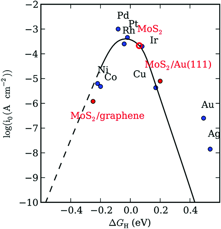 | ||
| Fig. 8 Volcano plot of various elements with respect to ΔGH*. Reproduce from ref. 129. | ||
The hydrogen coverage (ratio of hydrogen to sulfur atoms) on the top surface of the S-layers of MoS2 was found to be 1/16. Moreover, the ΔEH* of the H-atom on the surface of MoS2 can be defined by eqn (12).
 | (12) |
In 2005, Hinnemann and co-workers performed seminal work on MoS2 towards the HER and reported that the edge of Mo (10![[1 with combining macron]](https://www.rsc.org/images/entities/char_0031_0304.gif) 0) in MoS2 is very active for the HER due to its low ΔGH* value. DFT studies predicted that the binding energy towards H+ for MoS2 is +0.08 eV, which is close to that of noble metals such as Pt, at only its edge site. However, its catalytic activity is somehow limited given that the basal plane being relatively inert because it is less conducting although the exposed S edges are the active sites for electron transfer.132 Specifically, the defected S-edges play an important role in the HER for MoS2. Typically, the HER activity of MoS2 mainly depends on its size, edge active sites and number of layers. Thus, it is necessary to engineering MoS2 with efficiently exposed unsaturated S-sites to obtain electrocatalysts with high HER activity.
0) in MoS2 is very active for the HER due to its low ΔGH* value. DFT studies predicted that the binding energy towards H+ for MoS2 is +0.08 eV, which is close to that of noble metals such as Pt, at only its edge site. However, its catalytic activity is somehow limited given that the basal plane being relatively inert because it is less conducting although the exposed S edges are the active sites for electron transfer.132 Specifically, the defected S-edges play an important role in the HER for MoS2. Typically, the HER activity of MoS2 mainly depends on its size, edge active sites and number of layers. Thus, it is necessary to engineering MoS2 with efficiently exposed unsaturated S-sites to obtain electrocatalysts with high HER activity.
Interestingly, Kong and his group introduced more freshly exposed active sites on 2D MoS2 by engineering nanosized MoS2.133 The additional active sites are beneficial towards the intermediate adsorption of H, dramatically boosting the HER performance of 2D-MoS2 in both acidic and alkaline electrolytic solution. As illustrated in Fig. 9a–d, by employing a simple annealing method, the old molybdenum and sulfur atoms (marked area) present in 2D-MoS2 underwent a vaporization treatment and were replaced with fresh inner active edges with no alteration in the 2D structure of MoS2. Consequently, the new 2D-MoS2 possessed a greater density of under-coordinated S sites, exhibiting an enhanced ECSA and mass-normalized activity together with superior durability, and thus significantly improved HER activity. Upon heat treatment, the current density of the engineered 2D-MoS2 reached up to 440 mA cm−2 at a more positive onset potential compared that required for pristine MoS2. Besides engineering the edges of MoS2 through annealing treatment, designing defect-rich MoS2 through hydrothermal treatment on a substrate is another strategy for establishing highly exposed edge sites. Xie et al. constructed defect-engineered MoS2 catalysts with a controllable thickness, in which ultrathin nanosheets of MoS2 were vertically aligned to construct a nanowall structure.134 This MoS2 nanowall catalyst exhibited a high current density of 310 mA cm−2 at η = 300 mV with a low onset over potential of 85 mV. Its superior catalytic performance is attributed to its freestanding vertical channels, which are beneficial for ion penetration, and the presence of a rough surface together with highly exposed active edges. Nevertheless, it is still a challenge to design 2D-MoS2 with rational and controllable active sites. Accordingly, various strategies such as surface modification, morphological variation, phase and structure control, and fabrication of hybrid materials have been employed to increase the intrinsic activity and electrical conductivity of MoS2, thus increasing its active sites. Among the various achievements, here we only focus on the use of hybrid materials through hierarchical structures based on 2D/2D heterostructures. To date, a large number of HER studies has been reported on 2D MoS2-based 2D/2D heterostructures and few these studies of are detailed here.
 | ||
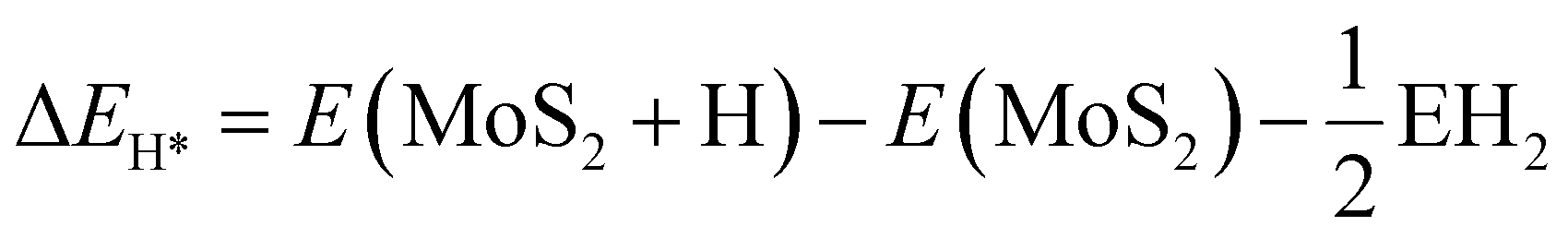
| Fig. 9 Structural representation of the edge of pristine MoS2 nanosheets in (a) top and (b) side views, and structural model of annealed MoS2 nanosheets in (c) top and (d) side views (Mo and S atoms are represented by blue and yellow balls, respectively). Reproduced with permission.133 (e) Polarization graph and (f) corresponding Tafel slope of various catalysts together with commercial Pt/C electrode in 1.0 M KOH and (g) hydrogen adsorption free energy plot for neat MoS2 MP and MoS2/GHS. Reproduced with permission.73 (h) Illustration of the catalysis mechanistic pathway for alkaline-mediated HER over Co-BDC/MoS2 hybrid, (i) polarization curves and chronopotentiometric response (inset) of Co-BDC/MoS2. Reproduced with permission.134 (j) Free-energy diagram for the HER and (k) calculated total electronic density of states for MoP, MoS2 and MoP/MoS2 heterostructures. Reproduced with permission.106 | ||
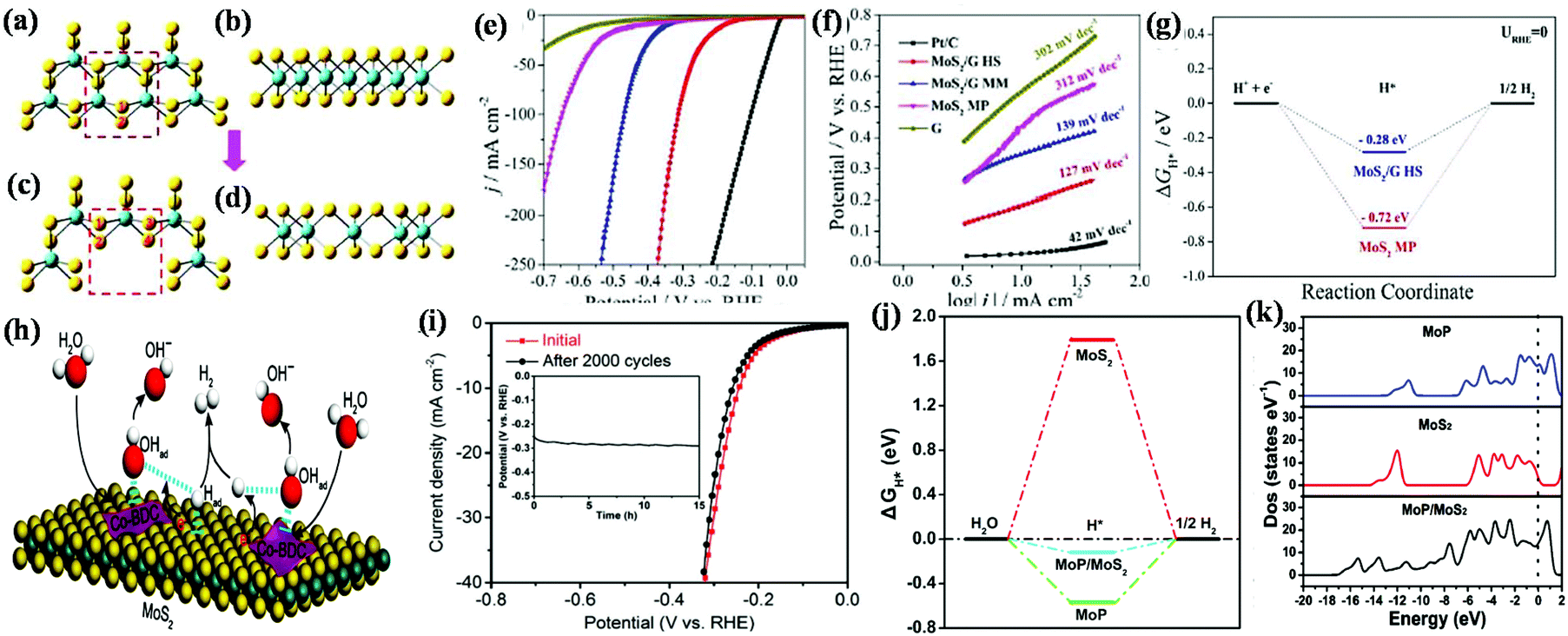
Yu and co-workers established an MoS2/graphene 2D/2D hetero-layered electrocatalyst towards electrocatalytic HER using both acidic (0.5 M H2SO4) and alkaline (1.0 M KOH) electrolytic solution and observed better HER activity in the former.73 According to the LSV data, it was deduced that a current density of 10 mA is achieved for the MoS2/graphene heterostructure at an overpotential of only 180 mV in acidic condition and 183 mV in alkaline solution (Fig. 9e), which is much lower than that obtained for neat MoS2, i.e., overpotential of 383 mV in acidic solution and 436 mV in alkaline solution, respectively. Furthermore, the catalytic performance toward the HER was evaluated through the Tafel slope, which was found to be 79 mV dec−1 and 127 mV dec−1 for the MoS2/graphene heterostructure in acidic and alkaline condition (Fig. 9f), and the corresponding Tafel slope value obtained for the neat MoS2 was about at 219 mV dec−1 and 312 mV dec−1, respectively. The superior HER performance of 2D/2D MoS2/G HS was due to the formation of an intimate face-to-face contact through the alternating layer-by-layer arrangement between 2D-MoS2 nanosheets and 2D-graphene, which led to more unsaturated atomic edge active sites contacting with the electrolyte and abundant defects between the 2D/2D interface of MoS2 and graphene. This layer-by-layer arrangement also has a great influence on the electronic state, which favoured the transfer and separation of charges, thus improving the electronic conductivity at the coupled interface. The increase in the number of edge active sites arose from the expanded interplanar distance (1.104 nm) for MoS2/graphene compared to that of MoS2 (0.615 nm), which is beneficial for the adsorption and desorption of hydrogen at the electrode electrolyte interface. The experimental study revealed that the 2D/2D MoS2/graphene HS exhibited superior wettability upon exposure to the electrolyte, which is beneficial for the availability and participation of more active sites in the HER. The smaller contact angle between MoS2 and graphene in the 2D/2D heterostructure than MoS2 improved the electronic conductivity at the coupled interface, facilitating the easy transfer and separation of charges at the interface. The high HER performance was also predicted by DFT studies through the three-state diagram (Fig. 9g) for the non-expanded pristine MoS2 and interlayer-expanded 2D/2D MoS2/G heterostructures. According to DFT, the ΔGH* (a powerful parameter for evaluating the adsorption and desorption process) was −0.72 eV for MoS2 and −0.28 eV for the 2D/2D heterostructure, where the lower potential suggests a lower energy barrier for the fast release and adsorption of hydrogen in the heterostructure, thus improving the rate of the HER.
Inspired by some theories, Zhu and co-workers introduced a 2D-MOF (Co-BDC)/MoS2 interface for alkaline HER (1 M KOH solution), in which Co-BDC with the optimum binding strength to H2O and hydroxyl promoted the sluggish water dissociation rate, while MoS2 enhanced the production and adsorption of hydrogen atoms at the hybrid interface.135 Importantly, the introduction of Co-BDC (acts as an electron donor) in MoS2 not only improved the alkaline HER, but also induced a partial phase transfer from 2H to 1T, which lowered the additional energy barrier. Fig. 9h illustrates the overall mechanism for the alkaline HER, which proceeds through the adsorption of hydroxyl, H2O and H* followed by the dissociation and desorption of H2O and H2 molecules, respectively, on the 2D-MOF (Co-BDC)/MoS2 hybrid nanosheets. The aforementioned electrocatalyst achieved an excellent current density at a very low overpotential. In addition, the long-term durability of the 2D-MOF (Co-BDC)/MoS2 hybrid was assessed to verify its stability in alkaline solution. Both the cyclic voltammetry and chronoamperometry curves (Fig. 9i) substantiating the excellent stability of the Co-BDC/MoS22D/2D hybrid nanosheet sample, even after 2000 cycles.
However, in some cases, the HER process is performed in neutral medium to avoid the problems arising in formidable strong acidic and alkaline environments, which also mitigates the environmental-related pollution. Wu et al. developed a 2D/2D MoP/MoS2 heterostructure that fulfils all the requirements needed for the HER process in a neutral environment, i.e., it possesses good conductivity for electron transfer, which is beneficial to decrease the Ohm resistance, plentiful active sites on the heterointerface present between 2D-MoP and 2D-MoS2 for H2O activation, and a porous environment on the surface for easy mass transfer, thus weakening the diffusion resistance.106 The neutral medium was balanced using 0.5 M H2SO4 with 1 M phosphate buffered solution and 1 M KOH. The MoP/MoS2 heterostructure exhibited an impressive current density at a low overpotential in neutral medium, which was much higher than that obtained for the bare MoS2 and for the reaction occurring in acidic and basic conditions. Furthermore, the MoP/MoS2 heterostructure also exhibited a good reaction kinetic mechanism with a low Tafel slope value (48 mV dec−1), which follows the Volmer–Heyrovsky reaction pathway. Considering that the neutral medium is governed through the adsorption of H2O molecules on the surface of the catalyst, the relative free energy of the hydrogen atom and H2O molecule was evaluated through DFT calculations, as shown in Fig. 9j. The calculated ΔGH* for hydrogen adsorption indicates that the MoP/MoS2 2D/2D heterostructure (−0.12 eV) is more favourable for the HER than bare MoS2 (1.79 eV). Furthermore, the higher H2O adsorption energy obtained for MoP/MoS2 (−1.38 eV) than its neat counterpart suggests that H2O can be easily adsorbed on the catalyst surface and is beneficial due to 2D/2D heterostructure. Furthermore, according to the density of state near the Fermi level, as shown in Fig. 9k, the fast electron transport in the HER process for MoS2/MoP was evaluated. Conversely, Liang et al. demonstrated that MoS2/black phosphorous exhibited superior activity in both acidic and basic medium.136
 | (13) |
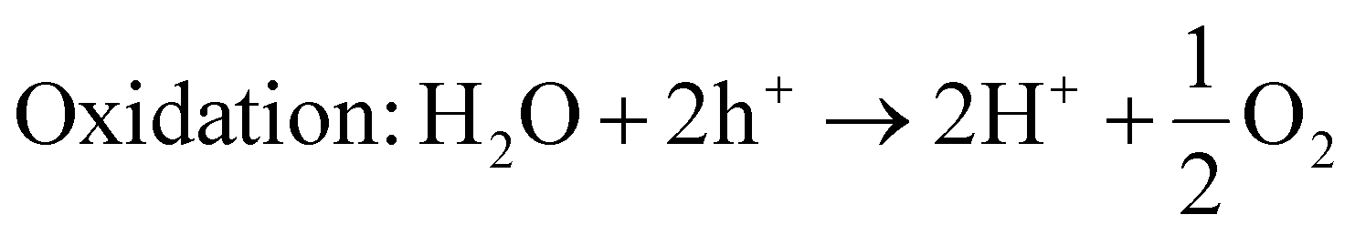
| Reduction: 2H+ + 2e− → H2 | (14) |
 | (15) |
 | (16) |
Generally, for the production of hydrogen and oxygen, the photocatalytic system mainly requires efficient photocatalysts and a light supply, which can be either a visible or UV-visible source. Under the action of photons, photogenerated charge carriers are generated and transferred to their respective band edge, i.e., electron jumps from the VB to CB edge, leaving a hole in the VB position. The electron in the CB of the photocatalyst is responsible for the reduction of water to produce hydrogen gas, while the hole in the VB facilitates the water oxidation reaction. This mechanism will happen when the CB position is located at a potential that is more negative than the potential required for the reduction of water, i.e., H+/H2 = 0 V vs. NHE at pH = 0 and −0.41 V vs. NHE at pH = 7, whereas the top level of the VB must be more positive than the redox potential of H2O/O2, i.e., 1.23 V at pH = 0 and 0.82 at pH = 7. In addition, the band gap must be higher than 1.5 V and not exceed 3.2 V.3,5,6 However, the utilization of noble metals or alloys is hindered by their high cost. Therefore, currently, it is urgent for researchers to develop competitive alternatives to noble metals. Despite the numerous photocatalytic materials, the unique candidate 2D-MoS2 plays an important role not only as a co-catalyst but also an excellent visible-light semiconductor with high hydrogen evolution activity due to its high surface to volume ratio, low cost, high catalytic activity, good stability and abundant active sites.45,46,137
The studies in the literature revealed that generally pure MoS2 as a photocatalyst exhibits no or negligible hydrogen evolution activity under visible light illumination. However, the photocatalytic hydrogen evolution activity of 2D-MoS2 is regulated by the number of layers of MoS2. With a decrease in the number of layers, the photocatalytic H2 evolution activity increases, which is maximum for a single layer of MoS2. This layer-dependent activity mainly originates from the exposed edges of MoS2 containing a large number of unsaturated dangling sulphur atoms (active sites for hydrogen generation), which bind the H+ ion very strongly.32 In addition, the band gap structure of 2D-MoS2 also plays a role in its photocatalytic H2 evolution performance. The wide band gap resulting from the quantum confinement effect of MoS2 (1.8–1.9 eV) and its low conduction band (CB) potential (0 to −0.12 eV) satisfy the conditions for the water reduction reaction (0 eV, at pH = 0 vs. RHE). To date, numerous works have been reported regarding the water reduction reaction using neat ultrathin MoS2. For example, Peng et al. fabricated a single-layer multiphasic MoS2 nanosheet keeping the optimum ratio between the 2H semiconducting phase and quasi metallic 1T’ phase and employed it directly as an efficient hydrogen evolution photocatalyst.130 According to the DFT study, they revealed that the in phase heterojunction between the 2H and 1T’ phase is responsible efficient charge transfer and separation, which are essential for photoactivity. Moreover, the suitable band gap of the 2H semiconducting phase is responsible for light absorption and charge generation, and the basal and edge sites at the 1T’ phase are the most favourable for hydrogen evolution. Further, considering the limited H2 production by pure MoS2, Wan and co-workers employed a novel approach for the synthesis of few-layer MoS2 nanosheets from an MoS2 stack with high yield through the facile solvothermal method followed by liquid exfoliation treatment.138 This synthetic procedure is beneficial for electronic and structural modification, which provides a large surface area together with additional exposed active edge sites, promoting the separation and transformation of photogenerated charge pairs to a greater extent. The solid monodispersed few-layer MoS2 nanosheets exhibited an excellent photocatalytic hydrogen evolution performance of 1241.3 μmol g−1 h−1. As described in Fig. 10a and b, the high photocatalytic effect is mainly attributed to the (i) formation of isolated nanosheets with a high surface area and exposed active sites for H+ adsorption and hydrogen evolution reaction, (ii) creation of lattice cracks on the inert basal plane due to the ultrasonication effect, followed by heat treatment, which added extra active sites, (iii) decrease in the number of layers of MoS2 nanosheets, which is beneficial for efficient charge separation and migration together with the creation of a direct band gap, (iv) structure change in which the MoS2 nanosheets possess a more negative CB potential for superior HER activity. Furthermore, the solid nature together with excellent stability and dispersibility in solution make the MoS2 nanosheets a great potential candidate for application in many fields. In addition, the as-obtained MoS2 nanosheets exhibited enhanced photoelectrochemical properties such as high transient photocurrent density, suggesting its superior photoelectric response, and the impedance measurement showed they possess good conductivity for promoting the transfer of photoinduced charge pairs in the photocatalytic reaction. Another few-layer MoS2 material towards photocatalytic hydrogen evolution was reported by Wang et al.139 They prepared few-layer (1–4 layer) MoS2 through a facile liquid-phase exfoliation strategy using a salt and organic electrolyte solution. It was found that the sodium tartrate-treated MoS2 exhibited a superior photocatalytic hydrogen evolution rate, i.e., 0.5 mmol g−1 h−1 compared to that of bulk MoS2.
 | ||
| Fig. 10 (a) Schematic illustration of the liquid exfoliation strategy for MoS2 by ultrasonication treatment and (b) disordered structure of few-layer MoS2 nanosheets. Reproduced with permission.138 (c) Production of H2 through the photoreduction of various BP/MoS2 samples and (d) schematic illustration of the charge transfer process in 2D–0D BP-10000/Pt and 2D–2D BP-10000/MoS2 photocatalyst. Reproduced with permission.103 (e) Energy diagram illustration of the photocatalytic mechanism over the 2D–2D MoS2/TiO2 photocatalyst and (f) H2 production yield on 0.50 wt% of different co-catalyst-loaded TiO2. Reproduced with permission.140 (g) Comparison of H2 production rates of MS-CN, SCN and MCN samples, [inset figure: representation of AQE for H2 evolution], (h) side-view illustration of MCN heterostructure with differential charge density (net electron accumulation and depletion are depicted by the yellow and navy regions, respectively) and (i) proposed mechanistic pathway diagram for photocatalytic H2 production reaction under visible light illumination. Reproduced with permission.110 | ||
Besides few-layer neat MoS2, the compositing of ultrathin neat MoS2 as a photocatalyst and co-catalyst with various UV- and visible-driven materials such as metal oxides, metal sulphides and carbonaceous materials has been studied recently. Here, we summarize a few recent reports on 2D/2D MoS2-based heterostructures towards photocatalytic hydrogen evolution. For example, Yuan et al. developed a 2D/2D black phosphorous/MoS2 heterostructure photocatalyst towards hydrogen evolution under visible light irradiation.103 The 2D/2D BP/MoS2 heterostructure exhibited a high current density (3.14 mA cm−2) together with high H2 evolution efficiency (1286 μmol h−1 g−1), as shown in Fig. 10c, and an apparent quantum yield of 1.2% in comparison with MoS2 nanosheets and bare BP sheets. In this study, the high photocatalytic activity is due to the unique 2D/2D interface (face contact) and was compared to a typical 0D/2D structure (point contact) by taking Pt as a 0D cocatalyst. According to the point of charge migration and charge pair separation, as given in Fig. 10d, it is obvious that the smart 2D/2D photocatalyst exhibits a much great contact nanointerface than 0D/2D, which provides a longer diffusion path length for the charge transfer and separation of photogenerated charge pairs, thus resulting in higher photocatalytic H2 evolution. Moreover, the driving force is another crucial factor in modulating the photocatalytic H2 production performance, and here the combination of quantum-sized BP (10000 rpm) with MoS2 provides a greater driving force, which lowers the CB to a more negative potential to achieve a high photocatalytic hydrogen evolution rate. In addition, Yuan et al. also applied a similar type of phenomenon to a 2D/2D binary (MoS2/CdS, MoS2/g-C3N4) system and 2D/2D/2D ternary system (g-C3N4/graphene/MoS2) through face-to-face contact and observed excellent photocatalytic activity compared to other photocatalysts.141–143 Compared to the 2D/2D MoS2-based heterostructure, we employ a 2D MoS2-based 2D/OD heterostructure to gain more insight into the structure–activity relationship. In this case, Chai et al. monitored the photocatalytic hydrogen evolution experiment using an MoS2/CdS composite in which MoS2 nanosheets were uniformly distributed on CdS nanospheres.144 The as-fabricated composite with only 5% MoS2 exhibited a hydrogen evolution rate of about 372 μmol h−1 with an apparent quantum yield of 7.31% under 300 W Xenon lamp illumination. The photocatalytic activity is attributed to the easy migration and separation of photogenerated charge carriers in the composite photocatalysts. Moreover, it should be noted that in comparison to binary 2D heterostructures, ternary 2D heterostructures provide a larger and more intimate 2D junction, which can effectively enhance the charge transfer rate, resulting in high photocatalytic activity.
Yuan et al. employed facile hydrothermal method for developing an MoS2/TiO2 (001) 2D/2D nanosheet heterojunction.140 The constructed typical 2D/2D heterojunction possessed a large and intimate interface between MoS2 and TiO2 and also boosted the separation and transportation efficiency of photogenerated charge pairs, which is attributed to the synergistic effect of MoS2 and TiO2. The energy diagram for the charge transfer process between MoS2 and TiO2 is illustrated in Fig. 10e. The 2D/2D interfacial structure provides a large contact area with abundant exposed active sites, which accelerate the rate of hydrogen evolution, achieving 2145 μmol h−1 g−1, a value 36.4-fold that of TiO2 nanosheets with an apparent quantum yield of 6.4% (360 nm). According to the data shown in Fig. 10f, it is also obvious that the MoS2/TiO2 (001) 2D/2D heterojunction is more active towards H2 production than noble metals such as Pt, Pd, Au, Rh and Ru-loaded TiO2 (001) nanosheets. Hence, it was proven that MoS2 acts as a better co-catalyst in 2D–2D systems than noble metals for hydrogen evolution activity.
Recently Dong et al. developed an S-doped g-C3N4/MoS2 2D/2D face-to-face heterojunction photocatalyst and observed its superior photocatalytic activity.110 The hydrogen evolution performance was investigated under visible light irradiation together with TEOA as a sacrificial agent. As shown in Fig. 10, the 2D/2D g-C3N4/MoS2 heterojunction achieved a high H2 production rate, i.e., 2120 μmol h−1 g−1 (Fig. 10g) together with a notable quantum yield of 5.7% (inset image) The high photocatalytic performance is attributed to the fast transportation of photogenerated charge carriers and efficient charge separation through the interface contact produced due to the face-to-face heterojunction between the two 2D components, which was also supported by the high photocurrent response. Moreover, first principle calculations of the differential charge density have become a crucial parameter to get an in-depth understanding about the charge separation efficiency based on photocatalytic activity. In this regard, Fig. 10h shows the charge redistribution at the face-to-face interface between 2D-S-g-C3N4 and 2D-MoS2, which clearly represents the accumulation and depletion of electrons in the MoS2 region, while the holes remain in the SCN region. The high efficiency is mainly due to the presence of S atoms, as seen in polarized field in the figure, facilitating the charge distribution at the interface region, which not only improves the light absorption capacity, but also allows efficient charge transfer. The possible H2 evolution mechanism proposed in Fig. 10i together with the energy band structure shows that the rapid channelization of photoexcited electron occurs from SCN to MoS2 through the face-to-face interface and the final H2 gas is evolved over the unsaturated S atoms at the MoS2 exposed edges. Thus, the above studies deduced that 2D/2D engineering between two 2D materials through face-to-face contact is one of the feasible ways to achieve charge separation for superior photocatalytic hydrogen production. The face-to-face 2D/2D interface structure for photocatalytic application has been widely employed by many researchers, and prior to this, more insight was gained by comparison with point contact.
4.2 Nitrogen reduction reaction
Similar to hydrogen, ammonia is an expectant “green fuel” candidate towards environmental sustainability, which is required to minimize the current issue based on the scarcity of fossil fuels.145,146 Due to its low liquefying pressure and high hydrogen density, ammonia also plays a vital role as an easy transportable promising carbon-neutral energy carrier with zero-balance greenhouse gases such as CO2 emission.147,148 However, the conversion of NH3 from N2 through the N2 fixation reaction via natural (nitrogenase enzymatic process) and artificial (i.e., industrialized Haber–Bosch process) processes is a practical problem nowadays due to the involvement of series of biochemical steps, which delay the reaction rate, increase the cost-effective, and reduce the safety.7,149 Thus, now it is of great significance to develop cost-effective, green and sustainable techniques for the production of NH3. Although a mimicking methodology has been investigated, i.e., traditional heterogeneous catalysis, electrocatalysis and photocatalysis-based NRR involving stable and noble-metal free catalysts at room temperature and atmospheric pressure is becoming a highly desirable and profitable artificial technique towards the reduction of N2 to NH3.7,75,146,148,150–153 For instance, the electrochemical NRR process involves the use of electrolytic cells together with different electrodes and electrolytes, which are powered by solar cells, wind turbines, etc., whereas in terms of photocatalytic NRR, the reaction is directly governed by sunlight or visible light. Although Mo-based catalysts exhibit a great performance towards the NRR as both photocatalytically and electrocatalytically active, to date, only a few studies have been reported, which are summarized in the following section. In the case of the photocatalytic and electrocatalytic NRR processes, both follow a number of mechanistic pathways, which can be determined through DFT analysis, to give the product.To design a potential catalyst with a low limiting potential (UL) towards superior photo/electrocatalytic N2 reduction, theoretical calculations based on machine learning are considered. According to DFT calculations, it has been predicted that the NRR performance is directly correlated with the five adsorbates (H, N2, N2H, NH, and NH2), whose binding energies are over 8 eV.154 The limiting potential that determines the minimum applied voltage to the exergonic NRR process follows one of two protonation steps, i.e., *N2 → *N2H and *NH → *NH2. Based on the DFT-computed free energy study, the UL can be represented as follows:
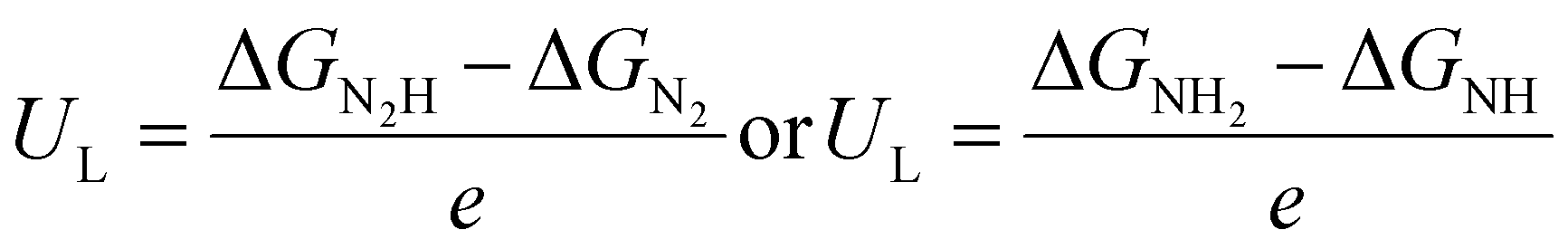
It has been determined from machine learning work that the catalytic surface, which fulfils the 4 to 6 d orbital occupation, can potentially lower the UL for the NRR reaction.154
![[triple bond, length as m-dash]](https://www.rsc.org/images/entities/char_e002.gif) N) and then captures one proton (H+) and one electron from the catalyst surface to give an adsorbed intermediate chemical species, i.e., *N
N) and then captures one proton (H+) and one electron from the catalyst surface to give an adsorbed intermediate chemical species, i.e., *N![[double bond, length as m-dash]](https://www.rsc.org/images/entities/char_e001.gif) NH, which is converted to the final NH3 product following the transfer of H+/e− pairs through the associative mechanism followed by the formation of different intermediate by-products such as N2H4 and N2H2.146,155,156 From a theoretical point of view, it has been elucidated that some metals such as Fe, Mo, Ru, Rh, Pt and Ir exhibit relatively optimized nitrogen binding capacity.155 Kim et al. investigated the distal mechanistic pathway through machine learning over several transition metals and found that the Mo surface with (110) plane exhibits the lowest UL value among them, i.e. about −0.92 V. Together with the low limiting potential over the Mo (110) surface, the binding energy difference, which estimates the adsorption competition of N2 and H components, is also more negative, i.e., −0.18 eV, which suggests a higher faradaic efficiency.154
NH, which is converted to the final NH3 product following the transfer of H+/e− pairs through the associative mechanism followed by the formation of different intermediate by-products such as N2H4 and N2H2.146,155,156 From a theoretical point of view, it has been elucidated that some metals such as Fe, Mo, Ru, Rh, Pt and Ir exhibit relatively optimized nitrogen binding capacity.155 Kim et al. investigated the distal mechanistic pathway through machine learning over several transition metals and found that the Mo surface with (110) plane exhibits the lowest UL value among them, i.e. about −0.92 V. Together with the low limiting potential over the Mo (110) surface, the binding energy difference, which estimates the adsorption competition of N2 and H components, is also more negative, i.e., −0.18 eV, which suggests a higher faradaic efficiency.154
Based on the demands regarding optimized N2 binding catalysts, Mo-based materials have been widely investigated as NRR electrocatalysts. Among them, 2D-MoS2 acts as an ideal catalyst for the NRR. Similar to the HER on MoS2, the edge sites of MoS2 are also more preferable towards the electrocatalytic NRR under ambient conditions. It has been considered that the elements Mo and S, which are the key elements of the nitrogenase-mediated reaction, play a vital role in the nitrogen fixation reaction. Accordingly, proof-of-concept regarding electrocatalytic NRR over MoS2 was investigated on accordance with DFT calculations, which mapped out the electronic environment of MoS2 through various energy profile diagramd.117,157 In this regard, in 2018, Zhang and co-workers reported their study based on the electrocatalytic NRR activity of 2D-MoS2 from a theoretical and experimental point of view to show whether the edge-site MoS2 are electrocatalytically active.117 According to the DFT studies, the isosurface of the deformation charge density of MoS2 was calculated to be a positively charged environment, i.e. +0.963|e|, around the edges of the Mo ion, which plays a significant role in the activation and polarization of N2 molecules. Also, the N2 molecules are generally activated and polarized at the positively charged centre, and thus based on DFT, they further deduced a free energy profile, as shown in Fig. 11a, from which the potential determining step (PDS) was studied. The PDS explains the reductive protonation of adsorbed N2 on the Mo edge surface with a lower limiting barrier of about 0.68 eV without applying any external potential, which is much higher in the case of some common metal surfaces, ranging from 1 to 1.5 eV. The relatively low barrier predicted by PDS for the Mo edge suggests the significant elongation of the N–N bond length, i.e., from *N2 (1.129 Å) to *NNH (1.221 Å), as shown in Fig. 11b, which accelerates the NRR. Consequently, the NN triple bond is easily weakened by the transformation of the charge from N2 to positively charged Mo-edge, resulting in N–Mo bond formation. This is clearly illustrated by the deformation charge density of *NNH supplied in Fig. 11c. Fig. 11d shows the NH3 yield together with the corresponding faradaic efficiencies (FEs) under the application of different potentials. An appreciable NH3 yield of 8.08 × 10⁻¹¹ mol s−1 cm−2 with a faradaic efficiency of 1.17% was achieved. The highest NH3 yield and faradaic efficiency were achieved at an optimum potential of −0.5 V, after which, the value markedly decreased, suggesting the competence adsorption nature of both hydrogen and nitrogen on the electrode surface. In addition, the MoS2/CC electrode possessed high stability given that there was no obvious change in NH3 yield after ten successive recycling tests. This relatively low barrier in terms of PDS on the Mo-edge further strengthens the claim that MoS2 is a potential catalyst for the NRR. Based on the abovementioned studies, although the MoS2 edge site is predicted to give an appreciable NH3 yield, some improvement is still needed regarding NRR selectivity due to its HER competence. Hence, Liu et al. prepared an ultrathin S-rich MoS2 nanosheet through Li intercalation and tested its performance towards the NRR in an acidic environment.158 The Li ion interacts with the S edge site of MoS2, which facilitates the adsorption of N2, and hence enhances the nitrogen reduction. According to the DFT study, it was found that Li–S interaction increases the N2 adsorption free energy from −0.32 to −0.70 eV and decreases the activation energy barrier of the reaction control step from 0.84 to 0.42 eV, and simultaneously, it also reduces the hydrogen adsorption free energy. The designed catalyst exhibited an NH3 yield rate of 43.4 μg h−1 mg−1 with the highest faradaic efficiency of 9.81%, while suppressing the HER yield.
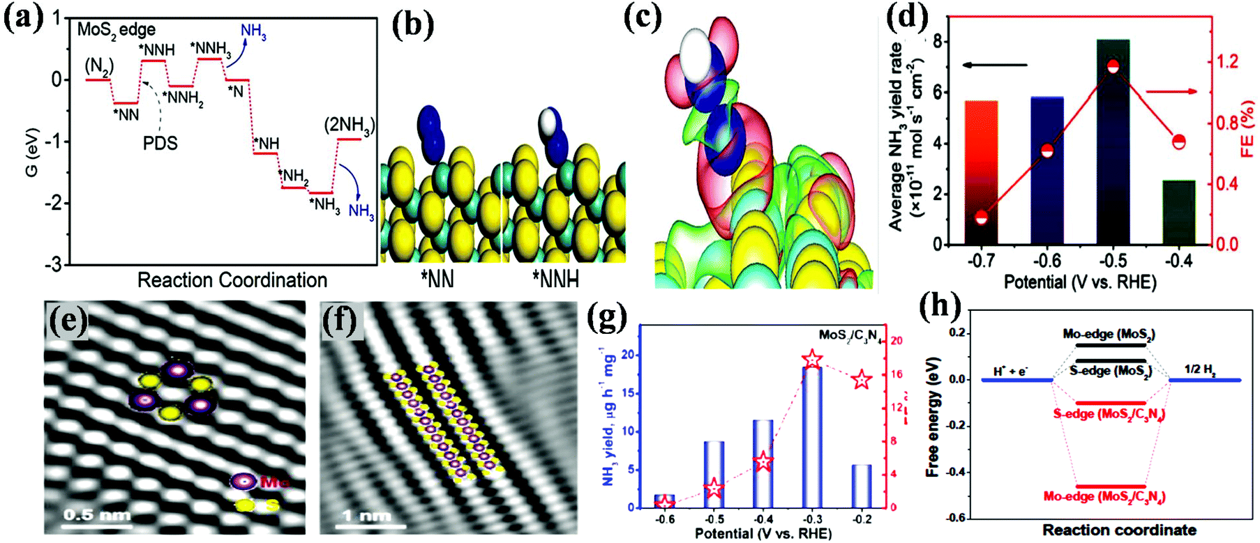 | ||
| Fig. 11 (a) Free-energy profile diagram at MoS2 edge site for the NRR, (b) structural representation of the key intermediates of the PDS, (c) deformation charge density diagram of *NNH, and (d) average NH3 yield and faradaic efficiency graph for MoS2/CC at different potentials. Reproduced with permission.117 (e) and (f) IFFT images of MoS2/C3N4, (g) NH3 concentration and faradaic efficiency plot for MoS2/C3N4 and (h) free energy diagrams of *H (ΔG*H) of MoS2 and MoS2/C3N4 on Mo-edge and S-edge sites. Reproduced with permission.159 | ||
Nevertheless, the electrocatalytic NRR activity of neat MoS2 nanosheets is still not satisfactory, and hence interfacial engineering via 2D/2D MoS2-based heterostructures is a powerful technique to meet the requirements for the NRR. Chu et al. designed a 2D/2D MoS2/g-C3N4 heterostructure for the NRR through a simple in situ hydrothermal method.159 According to the DFT analysis, the effective NRR performance is due to the face-to-face coupling interaction of MoS2/g-C3N4, which facilitates the stimulation of Mo edge sites towards the NRR and protects the NRR-active Mo-edge sites against the competing HER. However, the noise-filtered inverse fast-Fourier transform (IFFT) study, as shown in Fig. 11e and f, for MoS2/C3N4 revealed that over the hexagonal symmetry basal plane of 2D-MoS2, orderly stacked MoS2 layers are present together with exposed abundant Mo edge-terminating sites, which are believed to be the NRR active sites. Thus, to prove this hypothesis, the NRR performance over MoS2/C3N4 was evaluated in 0.1 M LiClO4 solution under ambient conditions. The best NH3 yield and the faradaic efficiency of the given electrocatalyst, as depicted in Fig. 11g, were obtained to be 18.5 μg h−1 mg−1 and 17.8%, respectively, at only −0.3 V of applied potential. However, beyond the potential of −0.3, the rate of NH3 together with the faradaic efficiency significantly decreased (e.g., at −0.2 V), which is ascribed to the competing HER on the surface of the electrode. During the course of the reaction, Chu et al. also depicted that the MoS2/C3N4 heterostructure electrocatalyst resulted in an excellent ammonia yield with good selectivity towards the NRR compared to neat C3N4 and MoS2 given that no N2H4 was detected. The reduction mechanism was thoroughly investigated through a DFT study (distal pathway). The free energy calculation followed by the potential limiting steps of all the intermediates suggested that MoS2/C3N4 exhibits a relatively low energy barrier for the reaction-controlling step, i.e., up to 0.55 eV for *N2 to *N2H, which changes to 0.62 eV for the pathway of *NNH2 to *N. The PDS value for MoS2/C3N4 is much more lower than that of neat MoS2, which suggests that the face-to-face interfacial contact created between 2D-MoS2 and 2D-C3N4 effectively stimulates the NRR activity by stabilizing *N2H. Furthermore, the protection of the NRR-active Mo-edge sites from the competing HER was also proven through the free energy study, as shown in Fig. 11h. Based on the calculated free energy data, ΔG*H was 0.08 and 0.15 eV for Mo and S-edge in pristine MoS2, respectively, whereas it was −0.46 eV for Mo edge and −0.12 eV for S-edge in the MoS2/C3N4 heterostructure. However, the great change in ΔG*H at the Mo-edge suggests the protection of the Mo-edge rather than the S-edge sites (favourable ΔG*H), which is unfavourable for the HER, hindering the formation H2 while allowing the NRR.
In addition, Li et al. developed a highly active and durable MoS2/RGO hybrid towards electrocatalytic NRR and found that it exhibited excellent selectivity for N2 conversion to NH3 under ambient conditions.160 The MoS2/RGO 2D/2D electrocatalyst achieved a high NH3 yield, i.e., 24.82 μg h−1 mg−1, with the corresponding faradaic efficiency of 4.56% at a potential of −0.45 eV. According to the DFT study, the authors suggested that the N2 adsorption on MoS2/RGO is more favourable than that on separate MoS2, which originated from the enhanced electron transfer. Further the PDS of the electron–proton coupling transferring process of *NHNH2 to *NH2NH2 with an energy barrier of 0.49 eV suggests the feasible generation of ammonia.
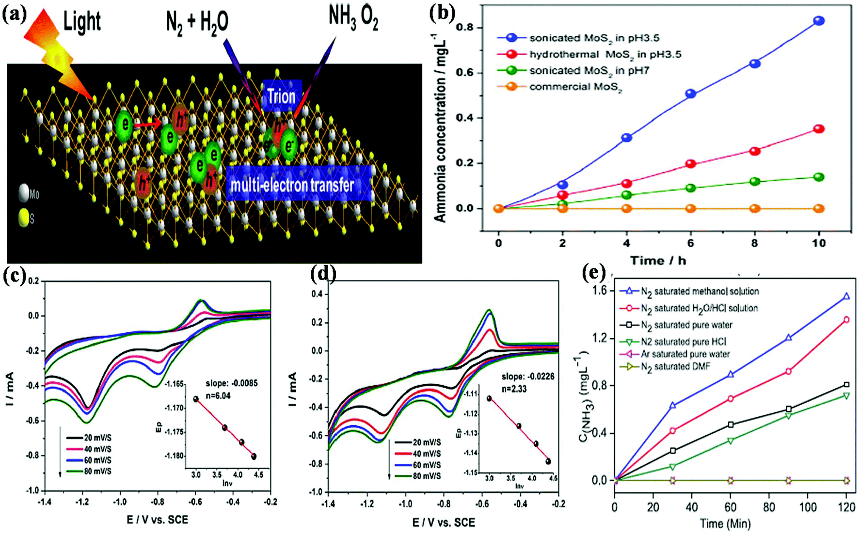 | ||
| Fig. 12 (a) Schematic representation of multi-electron N2 photoreduction process and (b) rate of ammonia concentration over various MoS2 samples mediated by different conditions. Cyclic voltammograms in N2-saturated 0.5 M Na2SO4 (pH = 3.5) at different scan rates for (c) sonicated ultrathin MoS2 electrode and (d) commercial MoS2 electrode. Reproduced with permission.50 (e) Yield of photoreduction of N2 fixation on 5% MoS2/MgIn2S4 heterojunction photocatalyst under various solvent conditions. Reproduced with permission.90 | ||
However, the N2 reduction efficiency obtained for pristine MoS2 is quite low compared to other photocatalysts, but from an experimental view, it has been seen that after compositing it with other 2D photocatalysts, its N2 reduction efficiency significantly increases. In this regard, our group designed a 2D/2D MoS2/MgIn2S4 heterojunction photocatalyst and tested its activity under visible light irradiation (250 W Hg lamps).90 The controlled photocatalytic N2 fixation experiment as illustrated in Fig. 12e, where the as-fabricated sample was tested under different reaction conditions using various scavenging units at the optimum pH. The investigated 2D/2D heterojunction photocatalyst achieved the highest concentration of NH4+ (1.54 mg L−1) with 10 vol% methanol–water system compared to that for distilled water (0.81 mg L−1) and DMF (no ammonia) due to the quick oxidation of methanol by h+, which produces CO2*− to facilitate the reaction easily. In contrast, by regulating the pH of the reaction, it was deduced that under a very high acidic environment (0.1 M HCl), the concentration of NH3 is quite low (0.72 mg L−1), whereas it increases with an increase in pH. It was observed for the HCl/H2O system with the optimum pH (pH = 3.6) that the ammonia concentration reached a high value (1.35 mg L−1). However, it was believed that in a highly acidic medium, the HER is dominant over the corresponding NRR, and in a moderate acidic medium, the generation of excess protons reduces the kinetic barrier for the NRR. Moreover, the given 2D/2D heterojunction photocatalyst possessed high selectivity towards the N2 reduction reaction with a 4.8-electron transfer process given that the peak for the bi-product (N2H4) was absent. The 2D/2D MoS2/MgIn2S4 photocatalyst achieved an excellent NRR performance and long-term stability was also observed for its photocurrent density. However, the overall photocatalytic performance depends on the 2D/2D combination through petals of the flower (2D-MgIn2S4) and a sheet (MoS2), which are attached via a face-to-face and face-to-edge fashion and the p–n heterojunction mechanism, favouring efficient charge migration and separation at the interface.
4.3 Carbon dioxide reduction reaction
As already discussed in the previous section, the excessive consumption of fossil fuels greatly increases the atmospheric carbon dioxide (CO2) level, and hence is regarded as the main culprit responsible for global climate change. The increase in CO2 level also disturbs the carbon cycle, leading to a severe greenhouse effect on the Earth's surface.1,2,4,164,165 Thus, nowadays, the foremost challenge faced by society is to conserve the environment for the future generation in the aspect of depletion of renewable energy sources with a reduction in the CO2 level in the atmosphere. In this scenario, the key issue is to design novel technologies that can relieve environmental problems by mitigating the CO2 concentration in the environment together with the production of sustainable energy using a clean and abundant strategies. Thus, to realize this fascinating blueprint, converting CO2 through the reduction process into renewable fuels together with value-added clean carbon-based nontoxic chemicals such as carbon monoxide (CO), hydrocarbons, alcohols, syngas, and formic acid has emerged as the most compelling pathway to build a sustainable recycling system by fulfilling the global energy demands.164–167 Nevertheless, CO2 is a stable, linear and chemically inert molecule bearing a huge energy gap of around 13.7 eV between its LUMO and HOMO, and hence the transformation of CO2 is a thermodynamically uphill reaction, demanding a significant energy input for the dissociation of the CO bond, which is around 750 kJ mol−1.
The process of CO2 reduction involves the adsorption and activation of a CO2 molecule on the surface of catalyst followed by a number of different reaction steps regulated through a 2, 4, 6, 8, 12 or more electron transfer pathway, which is kinetically very unfavourable.4 However, the photo/electro reduction of CO2 using efficient catalysts is becoming an economical and practical approach to solve the associated thermodynamic and kinetic hurdles. It has been concluded that both photocatalytic and electrocatalytic CO2RR are surface phenomena regulated through both protons and electrons.165,166
Besides water splitting, 2D-MoS2 has also emerged as an excellent candidate for the reduction of CO2 both photocatalytically and electrocatalytically. The superior catalytic efficiency of MoS2 in the CO2 RR has mainly emerged from its Mo and S-terminated edges and low work function value, which promote the efficiency of MoS2. By observing the periodic strip model, it was reported that in MoS2 there are two distinct types of edges, i.e., 010 and 100 edges, which are attributed to the S and Mo edges, respectively, and highly active towards the CO2 reduction reaction.168 In addition, it has been seen that in 2D-MoS2, the presence of active Mo-terminated edge sites stabilizes the intermediate products such as CHxOy produced during the CO2 reduction reaction.168–170
The CO2 reduction activity can be analysed via the binding energies of the CO2 reduction intermediates through computational analysis. For the CO2 reduction reaction, the computational hydrogen electrode model has received much attention to determine the mechanism of catalytic reactions and free energy profiles of the reaction intermediates proceeding through proton–electron (H+/e−) pair transfer by considering the effect of the electrode potential value on the reaction free energy.171,172 In addition, for each elementary step, the theoretical limiting potential (UL) is necessary, which determines the lowest external potential at which the reaction steps become exergonic together with the theoretical onset potential for the CO2 reduction reaction and is calculated as follows:
Accordingly, the most negative limiting potential is taken as the onset potential of the reaction. Chan et al. reported that product formation by the CO2 reduction reaction to CO follows the lowest free energy reaction path for MoS2 compared to other transition metals such as Au. From their study, at a specific surface coverage, MoS2 with Mo edges and S edges exhibited a UL value of −0.61 V and −0.15 V, respectively, which are smaller than that for Au (−0.78 V) at 0 V vs. RHE.168
However, the sluggish reduction potential needed for the conversion of CO2 into products with low gas adsorption ability limits its stability as a catalyst in its pure form. Additionally, the fast radiative recombination and low gas adsorption also affect the conversion efficiency of neat MoS2.173,174 Nevertheless, the practical applicability of MoS2 towards the CO2 reduction reaction can be improved by contributing to the role of exposed active sites on edge, defects and the terrace of the MoS2. The formation of heterostructures with other 2D materials can also be an effective way for the efficient CO2 reduction reaction. However, to date, there are only a few reports regarding the catalytic activity of MoS2 as a photocatalyst towards the CO2RR.
 | (17) |
 | (18) |
 | (19) |
 | (20) |
 | (21) |
 | (22) |
In comparison to the traditionally used noble metals, MoS2 acts as a promising cost-effective substitute for a superior CO2 electrochemical reduction performance. The high current density and low overpotential associated with the CO2RR are mainly due to the molybdenum-terminated edges and the catalytic performance is due to the high d-electron density and metallic character of MoS2.177
Lv et al. exfoliated bulk MoS2 into the nanosheet form by ball-milling followed by CVD and observed that the latter showed greater CO2 reduction activity. The exfoliated few-layer MoS2 nanosheets reduced CO2 to CO with a current density of 61 mA cm−2 at 1.1 V together with a faradaic efficiency of up to 41.2% at −0.9 V. The lower onset potential of ultrathin MoS2 (−0.43 V) in comparison to bulk MoS2 (−0.30 V) indicates a lower overpotential requirement for the reduction over the exfoliated form. They observed that the percentage of 1T-phase in the exfoliated MoS2 was much larger than its bulk form. Hence, decreasing the thickness of MoS2 can significantly increase its reduction ability. The mechanism behind the production of CO followed by the desorption of CO* on the surface of MoS2 is clearly shown in Fig. 13a and b, respectively. According to this figure, it was deduced that the catalytic site of MoS2 is the highly active Mo atoms on which CO2 is easily adsorbed after combining with H+/e−. Conversely, MoS2 possessing ΔG = 0.72 eV facilitates the easy desorption of CO* from its surface, resulting in the formation of products.178 The production of liquid hydrocarbon-containing products such as 1-propanol from CO2RR regulated through a high proton–electron process, i.e., 18 H+ and 18 e−, is kinetically challenging as the formation of two C–C bond is achieved. In addition, experimental studies revealed that during the electrochemical CO2 RR, water reduction to H2 evolution dominates over the CO2 reduction process given that water is present at a higher concentration compared to dissolved CO2 with a relatively low concentration. Accordingly, Francis and his group derived single-crystal MoS2, which yielded 1-propanol from CO2 in an aqueous electrolytic environment. Simultaneously, together with CO2 reduction, hydrogen was also produced by the reduction of water as the dominant electrolysis product. To gain insight into the selective production of 1-propanol over hydrogen evolution for a single-crystal MoS2 terrace, Fig. 13c provides the current density value via LSV measurement in both a CO2 environment (CO2 saturated electrolyte) and N2 environment (N2-purged phosphate buffer). The results indicate that the cathodic current obtained under the CO2 atmosphere is larger than that observed under the N2 atmosphere, which suggests that the reduction of CO2 is dominant over H2O reduction on the MoS2 single-crystal terrace. However, the production of 1-propanol was found to be larger for both the single MoS2 crystal and MoS2 thin film with low edge densities rather than that for the thin film containing high edge site densities. Thus, it was concluded that for the reduction of CO2 to 1-propanol, the MoS2 surface terrace is responsible not the edges of the thin-film MoS2. Experimentally, the MoS2 single crystal terrace displayed a faradaic efficiency of 3.5% at an applied potential of −0.59 V (vs. RHE) for the conversion of CO2 to 1-propanol, and that obtained for the MoS2 thin film with low edge site densities was around 1%. The experiment also revealed that together with 1-propanol as the major product, other minor products such as formate, ethylene glycol, and t-butanol are produced. The faradaic efficiency and the current density of major product, i.e., 1-propanol, together with formate are illustrated in Fig. 13d. Based on the experimental condition, it was concluded that production of 1-propanol involves the disulfidization of MoS2 followed by the coupling of intermediate species on the surface of the MoS2 single-crystal terrace.179
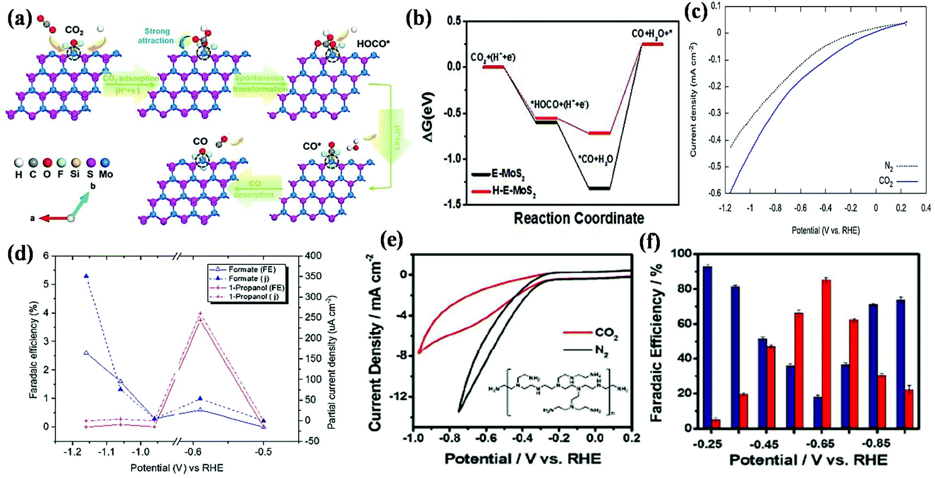 | ||
| Fig. 13 (a) Schematic illustration of mechanism for the formation of CO over H-E-MoS2 monolayers (Mo atoms are the catalytic sites represented by a dashed circle) and (b) free energy graph calculation for CO2 electroreduction to CO. Reproduced with permission.178 (c) Comparison of LSV data for an MoS2 single crystal in an N2 or CO2 environment and (d) potential-regulated partial current densities (dashed lines) and faradaic efficiencies (solid lines) of the CO2R products. Reproduced with permission.179 (e) CV plot over rGO-PEI-MoSx-modified GCE in CO2-saturated (red curve) N2-saturated (black curve), with a scan rate of 50 mV s−1 and (f) faradaic efficiency graph of CO (red bars) and H2 (blue bars). Reproduced with permission.180 | ||
Li et al. fabricated amorphous 2D-molybdenum sulfide (MoSX) on a polyethyleneimine (PEI)-modified rGO substrate and tested its CO2 reduction ability in aqueous NaHCO3 medium with high efficiency and selectivity. As revealed in Fig. 13e and f, the as obtained 2D/2D material selectively reduced CO2 to CO with a very low overpotential of 140 mV, while the maximum faradaic efficiency of 85.1% for the product was obtained at −0.65 V (RHE) with a TOF value of 2.4 s−1. They found that the PEI layer plays a major role in enhancing the catalytic activity of MoSx by suppressing the HER and stabilizing the CO2 intermediate during CO2 reduction.180
Due to the insufficient reduction potential required for converting CO2 into hydrocarbons, the MoS2 photocatalyst exhibits negligible activity towards CO2 reduction. Indeed, Geioushy and co-workers developed a 2D structured MoS2 sheet by employing a hydrothermal method followed by annealing. The photoreduction of CO2 proceeded under UV light irradiation and the formation of product, i.e., methanol and acetaldehyde, with hydrocarbon selectivity was controlled by choosing a different aqueous solution such as 0.5 M NaHCO3, NaOH and NaCl. The as-fabricated 2D MoS2 with a stacked-layer exhibited superior CO2 photoreduction conversion to different hydrocarbons such as methanol of 109.5 μmol g−1 (in 0.5 M NaHCO3 aqueous solution) and acetaldehyde of 19.2 μmol g−1 (in 0.5 M NaCl aqueous solution), as shown in Fig. 14a. The variation in the different hydrocarbon products was mainly governed through the effect of the various solvents used as the scavenging unit. The selectivity of the product depends on the anion effect of the solvent, which delays the charge carrier recombination. It was observed that the use of 0.5 M NaHCO3 solution resulted in the selectivity of CO2 photoreduction towards the production of CH3OH, accelerated through a 6-electron process. The selectivity for the production of CH3OH is attributed to the formation of HCO3− ions, which inhibit the charge pair recombination and also initiate multiple reaction pathways originating from the production of various intermediates such as formate ions followed by formyl anion. Alternatively, the production of methanol can also proceed via a 10-electron process, which can be due to the dimerization of the intermediates. The overall CO2RR reaction mechanism together with the reduction potential and multielectron participation over the undecorated 2D MoS2 sheet is depicted in Fig. 14b. It was also observed that with a change in the solvent from NaHCO3 to NaOH and NaCl, the production of methanol somewhat decreased followed by an increase in acetaldehyde upon CO2 photoreduction. The anion, i.e., OH− and Cl−, present in the respective solvent behaves as a hole scavenger and efficiently separates the photogenerated electron–hole pairs by accumulating more electrons on the MoS2 surface for the dimerization of two carbon species, resulting in the formation of CH3CHO. The high photocatalytic performance is attributed to the 2D structure morphology of MoS2, which boosts the transportation of electrons throughout the MoS2 sheet and also facilitates the reduction of adsorbed CO2 molecules.173
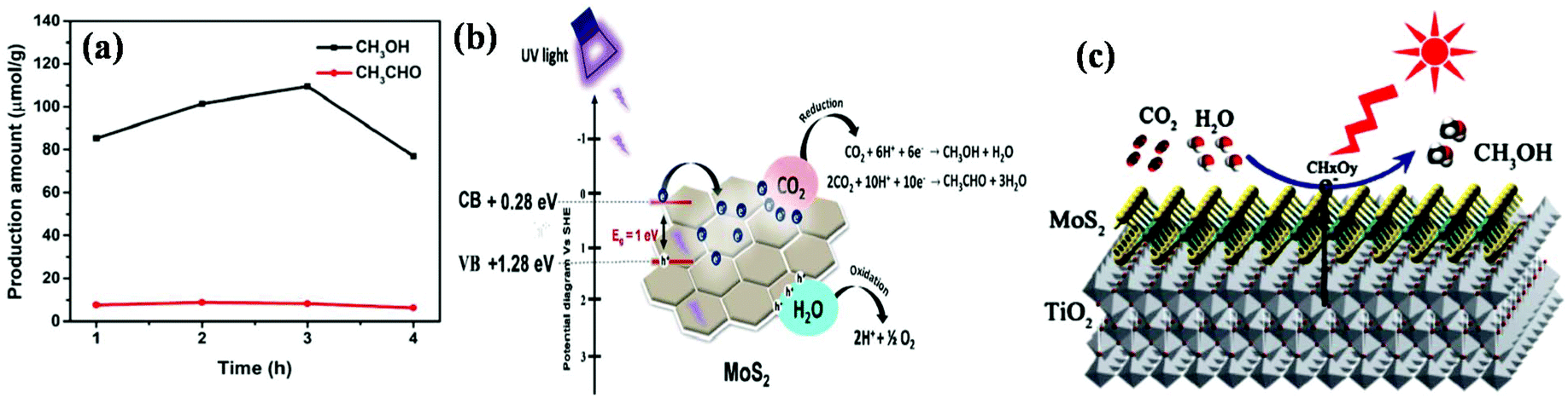 | ||
| Fig. 14 (a) Rate of CO2 reduction by MoS2 sheets in 0.5 M NaHCO3 and (b) schematic representation of the mechanistic pathway for photocatalytic CO2 reduction over MoS2 sheets. Reproduced with permission.173 (c) Schematic illustration of the photoreduction of CO2 to CH3OH in the MoS2/TiO2 heterostructure. Reproduced with permission.170 | ||
Further, Tu et al. designed a 2D MoS2/TiO2 hybrid nanojunction, in which 2D-MoS2 nanosheets were grown on a TiO2 nanosheet via an in situ method. The as-fabricated 2D nanojunction exhibited enhanced and selective CO2 photoreduction, resulting in CH3OH as the product in an aqueous NaHCO3 solution. The photocatalytic performance was tested under UV-visible light with CO2-saturated 1 M NaHCO3 aqueous solution as the scavenger. The MoS2/TiO2 hybrid nanosheets with an MoS2 content of 0.5 wt% selectively produced 10.6 μmol g−1 h−1 of CH3OH, which is 2.9 times greater than that for TiO2. The high photocatalytic efficiency is due to the unique coupling of MoS2 and TiO2 and the presence of Mo-terminated edges, which make it somewhat metallic, and also due to the presence of a high d-electron density, stabilizing the CHxOy intermediate during the CO2RR under UV-Vis light illumination via electrostatic attraction. This type of 2D/2D hybrid nanojunction creates a compact contact, which is beneficial for the quick transfer of photogenerated electrons from TiO2 to the Mo sites of MoS2 with a high d-electron density to enhance the lifetime of the charge carriers and reduction efficiency. The mechanism for photoreduction involves the binding of negatively charged intermediate species such as HCOO− and CHO− with the positively charged Mo cations through electrostatic attraction. The CO2 reduction performance was also compared with the novel metal-loaded TiO2 nanosheets, but the rate of reduction of CO2 to the main product was lower than that for MoS2-loaded TiO2. The overall CO2 reduction mechanism is schematically illustrated in Fig. 14c.170
To achieve an ideal bandgap and exposed active sites towards superior photocatalytic CO2 reduction to value-added hydrocarbons, interfacial engineering between two 2D layered materials has emerged as a productive strategy. Qiu and co-workers employed electrostatic self-assembly as a cost-effective strategy for developing a series of 2D layered LDH-MoS2 heterostructured nanocomposites, providing a novel route to produce syngas with tunable a H2:CO proportion via CO2 photoreduction under visible light irradiation. The electrostatic interaction is created throughout the reaction by the combination of positively charged LDH with the negatively charged surface of MoS2, which provides a large interface for the CO2RR, and by controlling the interface-rich heterostructure catalyst concentration, the production of the syngas (H2:CO) proportion can be tuned. The experiment revealed that both LDH and MoS2 individually were unable to produce syngas with a modulated H2:CO proportion; however, with a change in the loading percentage of MoS2 from 0.1 to 0.3 in the LDH/MoS2 heterostructure, the H2:CO proportion was modulated, and with 0.30%, the proportion changed from 1:1 to 9:1. The origin of CO production from CO2 was traced via a 13CO2 isotopic experiment and analyzed through GC-MS spectrometry based on the signal obtained at m/z = 29, which is attributed to 13CO. In addition, the overall experiment was conducted in the presence of a photosensitizer (H2O/acetonitrile with [Ru(bpy)3]Cl2·6H2O) and sacrificial agent (TEOA), which accelerate the CO2 photoreduction mechanism. Theoretical calculation of the binding energy and DFT calculation were employed to determine the charge transfer between the heterojunction and structure–activity relationship during the CO2 photoreduction. The lower work function value of LDH (3.946 eV) than that of MoS2 (5.92 eV) suggests that the flow of electron occurs from LDH to MoS2 through the Mo–O–S chemical bond to maintain the equilibration of the Fermi level. A new type of charge distribution suggested electron accumulation near the LDH surface and predicted the flow of electrons from MoS2 to the LDH surface. Moreover, the narrower bandgap energy observed via DOS calculation for the MoS2/LDH heterojunction indicates the strong interaction between LDH and MoS2. Prior to light illumination, firstly, photogenerated electrons are excited from the HOMO to LUMO of the Ru complex and then transferred to the CB of the LDH and MoS2via the interface and selectively reduce CO2 to CO at the LDH surface and H2 at both the LDH and MoS2 surface by coupling with active hydrogen species.182 Besides, Kumar et al. designed an advanced functionalized nanomaterial, i.e., pyrrole-promoted RGO-MoS2 nanocomposite, for the efficient photoreduction of CO2 into solar fuels and observed superior photocatalytic CO2 reduction.183 In comparison, Xu et al. fabricated a 1D/2D TiO2/MoS2 hybrid nano-structure in which a 2D-MoS2 sheet vertically and uniformly covered 1D-TiO2 electrospun fibres, which exhibited superior activity for CO2 reduction to CH3OH and CH4 under UV-visible light irradiation. The developed 1D/2D nanohybrid achieved the production rate of 2.6 and 2.55 μmol g−1 h−1, corresponding to CH4 and CH3OH, respectively, together with an apparent quantum yield of 0.16%. The photocatalytic activity is attributed to the presence of 2D-MoS2, which enhances the light-harvesting properties of TiO2 by increasing its absorption range.184 In addition, other 2D–3D (MoS2/SiC185 and MoS2/TiO2186) have also been investigated for their CO2 reduction activity; however, 2D–2D MoS2-based materials for CO2 reduction not been researched on a large scale.
4.3 Other applications of 2D MoS2 and MoS2-based 2D/2D heterostructures
In addition to energy conversion, other practical applications over MoS2 have also been reported. To date, 2D-MoS2 has been extensively applied for the photodegradation of various pollutants, antibiotics and dyes due to its absorption properties in a wide range of light, strong absorptivity properties, non-toxicity, stability against corrosion and environmentally friendly nature.47 Ji and co-workers constructed a 2D/2D MoS2/CeO2 heterojunction photocatalyst,102 which exhibited stronger degradation ability (88.5% in 120 min) than its neat counterpart with a huge reduction in the intensity of the peak in the UV-Vis spectrum with time, which shifted from 277 nm to 260 nm. In addition, the high surface to volume ratio, rapid response with improved sensitivity and low power consumption behaviour of 2D-MoS2 materials have stimulated substantial research for different sensing applications such as biosensors, chemical sensors, electrochemical sensors, and gas sensors.187 Hwang and co-workers developed a vertically aligned 2D-MoS2 nanofilm with highly exposed Mo and S dangling bonds through the CVD method and tested it for the detection of heavy metals (Pb2+) in tap water.188 The material exhibited superior detection sensitivity with a limit of detection of 0.3 ppb at 180 s deposition time with a relative standard deviation of 3.1%. Again, various gas molecules such as NO, H2, and NH3 can be easily adsorbed on the surface of MoS2. Additionally, 2D-MoS2-based heterostructures have also been explored for the detection of different biomolecules and analytes in the environment. More importantly, in dye-sensitized solar cells (DSSCs), 2D-MoS2 has exhibited superior performances due to its high electrocatalytic activity and high conductivity. Vikraman et al. fabricated a highly efficient layered MoS2 counter electrode, which acts as a low-cost alternative to Pt-based DSSCs. Under 100 mW cm−2 (AM 1.5) stimulated solar irradiation, a high power conversion efficiency of 7.14% was achieved, which is nearly equal to that of 8.73% observed for the Pt/FTO counter electrode through the reduction of tri-iodide to iodide.189Furthermore, 2D-MoS2 has been extensively investigated for its application in electronic devices as a channel material mainly due to its atomically thin structure, which exhibits exceptional electronic properties including variable band gap and suitable charge carrier mobility.190,191 Due to the presence of a band gap in 2D-MoS2 compared to bulk MoS2, its conductivity can be modulated, which is feasible for the electrostatic control of this material and make it a suitable candidate for application in the field of electronic devices, especially field-effect transistors (FETs) and low-power electronic devices.192 It has been demonstrated that 2D-MoS2 as an FET at room temperature exhibited an on/off drain current ratio of 108 with an enhancement in mobility of up to 200 cm2 (V s)−1.193 Inspired by its direct band gap (∼1.9 eV) with semiconducting behaviour and excellent mechanical properties such as flexibility and stretchability, 2D-MoS2 is attracting great attention in the area of optoelectronic devices such as light sensing photodetectors, LEDs, and solar cells.194,195 Zhai et al. designed an NiTe2/MoS2 2D/2D vertical heterostructure towards the study of a back-gated FET and photodetector as an electronic and optoelectronic device, respectively. The as-obtained stack layered materials resulting from the van der Waals epitaxial heterostructure provided enhanced electronic contact at the heterointerface, which enhanced the optoelectronic responses by 5 times and the electronic behaviour compared to that of neat MoS2.98 Besides, 2D-MoS2 is widely used in the field of energy storage devices especially in supercapacitor applications due to its tunable interlayer distance and long cycle durability. The presence of a stacked-lamellar sheet-like structure together with suitable oxidation states over Mo, i.e., +2 and +6, 2D-MoS2 exhibits electrical double layer capacitance behavior. Considering that the van der Waals attraction present between the stacked layers is weak, the various guest components such as ions/electrons can be easily intercalated throughout the layer, thus increasing the charge discharge behaviour of the material together with its capacitance.196,197 A novel intercalated nanostructured fibre electrode was developed by Wang et al. via the combination of MoS2 sheets, which exhibited a high pseudocapacitance value, with graphene with high electrical conductivity. The aforementioned graphene/MoS2 fibre electrode with an intercalated nanostructure possessed a high ion-accessible surface area, resulting a high specific capacitance of 368 F cm−3 at a current density of 0.1 A cm−3 when the MoS2 content was up to 33.98%. In addition, the fibre electrode exhibited cycle stability of 80% for 8000 cycles with a current density of 12.8 mW h cm−3.198 Moreover, recently, Kirubasankar and co-workers constructed a 2D MoS2/MXene nanohybrid interlayer structure, which restricted the electrostatic attraction and prevented the self-stacking of individual layers, thus providing high mass transfer between the electrolyte-electrode interface. The MoS2/MXene nanohybrid presented a superior specific capacitance about 583 F g−1 with a rate capability of 2.5% at 1 A g−1 and 96.5% cycle stability up to 5000 cycles at 5 A g−1.199 The various photocatalytic and electrocatalytic applications towards energy conversion using 2D-MoS2 and its 2D/2D heterostructures are presented in Table 1.
| Photocatalyst | Synthesis method | Amount of photocatalyst and volume of sacrificial agent | Irradiation light source | Rate of hydrogen evolution | Apparent quantum yield/Efficiency (AQY/AQE) | Ref. |
|---|---|---|---|---|---|---|
| (i) Photocatalytic hydrogen evolution reaction | ||||||
| Few-layer MoS2 nanosheets | Facile solvothermal treatment coupled with the liquid exfoliation strategy | 50 mg in 100 mL of aqueous solution containing 0.35 M Na2S and 0.25 M Na2SO3 | 300 W Xe | 1241.3 mmol g−1 h−1 | — | 138 |
| Few-layer MoS2 nanosheets | Liquid-phase exfoliation strategy | 3 mg in 15% TEOA aqueous solution | 300 W Xenon lamp | 0.5 mmolg−1 h−1 | — | 139 |
| In-plane multiphasic 2D MoS2 nanosheets | Chemical intercalation method | 40 mg in 40 mL of deionized water with 0.01 M lactic acid | 200 W Hg lamp | 1.5 mmol h−1 g−1 | AQY = 12.90% | 130 |
| MoS2/CdS | Ex situ adsorption-calcination | 10 mg in 20 mL H2O + 5 mL lactic acid | 300 W Xenon lamp (λ ≥ 420 nm) | 18.43 mmol h−1 g−1 | AQE = 3.4% | 92 |
| MoS2/g-C3N4 | Ex situ | 50 mg in 200 mL of 10 vol% glycerol solution | 500 W Xenon lamp | 10000 μmol h−1 g−1 |
— | 200 |
| MoS2/g-C3N4 | Ex situ ultrasonic assisted strategy | 20 mg in 20 mL water/methanol (4:1 v/v) solution |
300 W Xenon lamp | 1497 μmol h−1 g−1 | AQY = 3.3% | 121 |
| ZnIn2S4/MoS2 | Ex situ electrostatic self-assembly process | Lactic acid | Visible light | 4.974 mmol g−1 h−1 | — | 95 |
| Black phosphorous/MoS2 | In situ solvothermal method | 10 mg in 250 mL of 0.1 M Na2S and 0.1 M Na2SO3 aq. solution | 300 W Xenon lamp | 1286 μmol h−1 g−1 | AQY = 1.2% | 103 |
| MoS2/Ti3C2 | In situ hydrothermal method | 30 mg in 50 mL of methanol solution | 300 W Xenon lamp | 6144.7 mmol g−1 h−1 | — | 201 |
| MoS2/CdS | In situ hydrothermal method | 50 mg in 250 mL 0.4 M Na2S and 0.4 M Na2SO3 solution | 300 W Xenon lamp | 26.32 mmol h−1 g−1 | AQY = 46.65% | 141 |
| MoS2/g-C3N4 | In situ probe sonication-assisted liquid exfoliation | 50 mg in 250 mL of 0.1 M TEOA aqueous solution | 300 W Xenon lamp | 1155 μmol h−1 g−1 | AQY = 6.8% | 142 |
| MoS2/SnNb2O6 | In situ Hydrothermal method | 50 mg in 50 mL of 20 vol% methanol. | 300 W Xenon arc lamp | 12.9 μmol h−1 | — | 202 |
| CoMoS2/rGO/C3N4 | In situ solvothermal method | 100 mg in a mixed solution of TEOA and H2O (volume ratio equal to 1/5) | 300 W Xenon lamp | 684 μmol g−1 h−1 | — | 203 |
| g-C3N4/graphene/MoS2 | In situ hydrothermal method | 50 mg in 250 mL of 0.1 M TEOA solution | 300 W Xenon lamp | 317 μmol g−1 h−1 | AQY = 3.4% | 143 |
| Ti3C2 MXene/MoS2/TiO2 | In situ two-step hydrothermal | 10 mg in aqueous acetone with dissolved sacrificial reagent (TEOA) | 300 W Xenon lamp | 6425.297 μmol h−1 g−1 | AQY = 4.61% | 204 |
| S-Doped polymeric carbon nitride/MoS2 | One-pot hydrothermal-polymerization method | 50 mg in 10 vol% TEOA aq. solution | 300 W Xenon lamp | 2120 μmol h−1 g−1 | AQE = 5.7% | 110 |
| N-Doped MoS2/S-doped g-C3N4 | One-step thermal polycondensation method | 50 mg in 100 mL 10 vol% TEOA | 300 W Xenon lamp | 658.5 μmol g−1 h−1 | — | 205 |
| MoS2/CeO2 | In situ hydrothermal | 20 mg in 20 mL of 10 vol% methanol | 150 W xenon lamp | 508.44 μmol h−1 | — | 89 |
| MoS2/CaIn2S4 | In situ hydrothermal | 20 mg in 20 mL of 0.025 M Na2S and 0.025 M Na2SO3 aq. solution | 150 W xenon arc lamp | 602.35 μmol h−1 | Apparent Conversion Efficiency = 9.71% | 76 |
| MoS2/ZnIn2S4 | One-pot hydrothermal | 20 mg in 20 mL of 0.25 M Na2SO3 and 0.35 M Na2S aq. solution | 150 W xenon arc lamp | 379.1 μmol h−1 | Apparent Conversion Efficiency = 6.07% | 115 |
| MoS2/NiFe LDH | In situ electrostatic self-assembled chemistry | 30 mg in 30 mL of 10 vol% CH3OH aq. solution | 125 W medium pressure Hg lamps | 550.9 μmol h−1 | — | 104 |
| MoS2/MgIn2S4 | In situ hydrothermal method | 20 mg in 20 mL of 0.25 M Na2SO3 and 0.35 M Na2S aq. solution | 150 W Xenon arc lamp | 570.8 μmol h−1 | — | 90 |
| UiO-66-NH2 MOF/MoS2 | In situ hydrothermal method | 20 mg in 20 mL of 10% methanol solution | 300 W Xe arc lamp | 512.9 μmol h−1 | Apparent Conversion Efficiency = 3.84% | 113 |
| P-MoS2/CdS | In situ hydrothermal | 10 mg in 100 mL of 0.35 M Na2S and 0.25 M Na2SO3 | 300 W Xe lamp | 58.9 μmol h−1 | AQE = 19.0% | 206 |
| MoS2/Co–Al LDH | In situ hydrothermal | 50 mg in 80 mL methanol solution | 300 W Xe lamp | 17.1 μmol g−1 h−1 | — | 207 |
| MoS2/g-C3N4 | In situ solvothermal | 5 mg in 40 mL of 10% TEOA solution | 300 W Xenon arc lamp | 1787 μmol h−1 g−1 | — | 208 |
| Catalyst | Synthesis process | Electrolyte | Current Density (mA cm−2) | Over-potential (mV) | Tafel slope (mV dec−1) | Ref. |
|---|---|---|---|---|---|---|
| (ii) Electrocatalytic hydrogen evolution reaction | ||||||
| Defect-rich MoS2 nanowall | Hydrothermal | 0.5 M H2SO4 | 10 | 95 | 78 | 135 |
| Fractal-shaped single-layer MoS2 | CVD method | 0.5 M H2SO4 | 10 | 185 | 45 | 84 |
| Single-atom metal-doped MoS2 | One-pot hydrothermal method | 0.1 M H2SO4 | 10 | 60 | 96 | 209 |
| MoS2 nanosheets | Hydrothermal followed by annealing process | 0.5 M H2SO4 and 1 M KOH | 10 mA mg−1 | (i) Acidic = 171 (ii) alkaline = 162 | (i) Acidic = 54 (ii) alkaline = 68 | 133 |
| Surfactant-exfoliated 2D molybdenum disulphide | Liquid-phase exfoliation | 0.5 M H2SO4 | −4.96 | 420 | 94 | 210 |
| 2D MoS2 nanosheets | Hydrothermal method | 0.5 M H2SO4 | 25 | 280 | 90 | 88 |
| 2D MoS2 Thin Films | CVD | 0.5 M H2SO4 | 60 | 640 | 90 | 85 |
| FePS3/MoS2 | In situ Hydrothermal method | 1 M KOH solution and 0.5 M H2SO4 solution | 10 | (i) 1 M KOH = 175 (ii) 0.5 M H2SO4 = 168 | (i) 1 M KOH = 127 (ii) 0.5 M H2SO4 = 107 | 211 |
| Co-BDC/MoS2 | In situ sonication-assisted solution strategy | 1 M KOH solution | −10 | 248 | 86 | 134 |
| MoP/MoS2 | In situ Phosphorization | 0.5 M H2SO4, 1 M phosphate buffered solutions (PBS) and 1 M KOH | 10 | (i) Neutral = 96 (ii) alkaline = 54 (iii) acidic = 69 | (i) Neutral = 48 (ii) alkaline = 58 (iii) acidic = 61 | 106 |
| MoS2/black phosphorus | In situ | 0.5 M H2SO4, 1 M KOH and 1 M PBS | 10 | (i) Neutral = 258 (ii) alkaline = 237 (iii) acidic = 126 | (i) Neutral = 154 (ii) alkaline = 99 (iii) acidic = 68 | 136 |
| MoS2/N-doped graphdiyne | In situ solvothermal method | 0.5 M H2SO4 | 10 | 186 | 63 | 212 |
| MoS2/graphene | In situ self-assembly method via electrostatic attraction | 0.5 M H2SO4 and 1.0 M KOH | 10 | (i) Acidic = 180 (ii) alkaline = 183 | (i) Acidic = 79 (ii) alkaline = 127 | 73 |
| MoS2/graphene | Ex situ two-step sonication method | 6 M KOH | 25 | 125 | 41 | 213 |
| RGO/MoS2 | One-step hydrothermal method | 0.5 M H2SO4 solution | 100 | 150 | 52.5 | 214 |
| MoS2/graphene | One-step in situ solvothermal | 0.5 M H2SO4 | 10 | 94.2 | 140 | 215 |
| MoS2/g-C3N4 | One-pot method | 0.5 M H2SO4 | 10 | 140 | 45 | 109 |
| MoS2/carbon nitride | In situ hydrothermal | 0.1 M KOH | 10 | 153 | 43 | 61 |
| Photocatalyst | Synthesis method | Amount of photocatalyst and volume of sacrificial agent | Irradiation light source | Rate of NH3 synthesis | Ref. |
|---|---|---|---|---|---|
| (iii) Photocatalytic nitrogen reduction reaction | |||||
| Ultrathin MoS2 | Hydrothermal followed by ultra-sonication | 15 mg in 200 mL DI water + HCl solution (pH = 3.5) | 500 W Xenon lamp | 325 μmol h−1 g−1 | 50 |
| MoS2/biochar | In situ | 20 mg in 100 mL of DI water | 300 W Xenon lamp | 37.878 μmol g−1 h−1 | 216 |
| MoS2/MgIn2S4 | In situ two-step hydrothermal method | 15 mg in 50 mL distilled water + HCl solution (pH = 3.6) | 250 W Hg lamp | 2509.2 μmol h−1 g−1 | 90 |
| Catalyst | Synthesis method | Electrolyte | Rate of NH3 evolved | Faradic efficiency (%) | Potential (V) | Ref. |
|---|---|---|---|---|---|---|
| (iv) Electrocatalytic nitrogen reduction reaction | ||||||
| 2D-MoS2 | Hydrothermal followed by annealing method | 10 mg in 0.1 M Li2SO4 solution (pH = 3.0) | 43.4 μg h−1 mg−1 | 9.81 | -0.2 | 158 |
| MoS2 | Hydrothermal method | 0.1 M Na2SO4. | 8.08 × 10⁻¹¹ mols−1 cm−1 | 1.17 | −0.5 | 117 |
| MoS2/C3N4 | In situ | 0.1 M Na2SO4 | 19.86 μg h−1 mg−1 | 6.87 | −0.5 | 75 |
| MoS2/RGO | In situ hydrothermal | 0.1 M LiClO4 | 24.82 μg h−1 mg−1 | 4.58 | –0.45 | 160 |
| MoS2/C3N4 | In situ hydrothermal | 0.1 M LiClO4 solution | 18.5 μg h−1 mg−1 | 17.8 | −0.3 | 159 |
| Photocatalyst | Synthesis method | Amount of photocatalyst and volume of sacrificial agent | Light source | Main product | Yield | AQY/AQE | Ref. |
|---|---|---|---|---|---|---|---|
| (v) Photocatalytic carbon dioxide reduction | |||||||
| 2D-MoS2 sheets | Hydrothermal followed by annealing method | 0.1 g in 50 mL 0.5 M (i) NaHCO3, (ii) NaOH and (iii) NaCl aqueous solution | 150 W medium pressure mercury vapour lamp | (i) Methanol in 0.5 M NaHCO3 (ii) Acetaldehyde in 0.5 M NaCl | (i) 109.5 μmol g−1 (ii) 19.2 μmol g−1 | — | 173 |
| Polypyrrole/rGO-MoS2 | In situ wet chemical synthesis | 50 mg in 20 mL of 0.5 M NaHCO3 | 300 W Xenon lamp | (i) CO, (ii) CH4 (iii) H2 | (i) 3.95 μmol g−1 h−1 (ii) 1.50 μmol g−1 h−1 (iii) 4.19 μmol g−1 h−1 | AQE = 0.30% | 183 |
| MoS2/g-C3N4 | Ex situ hydrothermal deposition method | 50 mg in 100 mL deionized water | 300 W Xenon lamp | CO | 58.59 μmol g−1 for 7 h | AQY = 0.255% | 217 |
| MoS2/TiO2 | In situ hydrothermal | 0.1 g in 200 mL of 1 M NaHCO3 solution (pH = 8) | 300 W xenon arc lamp | CH3OH | 10.6 μmol h−1 g−1 | — | 170 |
| LDH/MoS2 | Ex situ electrostatic self-assembly | Photocatalyst (0.3 mg mL−1) and [Ru(bpy)3]Cl2 × 6H2O (3.3 mg) were suspended in 10 mL aqueous solution containing H2O:CH3CN:TEOA = 1:3:1 (V/V/V) |
300 W Xe lamp | (i) CO (ii) H2 | (i) 3617 μmol h−1 g−1 (ii) 6187 μmol h−1 g−1 | — | 182 |
| Catalyst | Synthesis method | Electrolyte | Main product | Current density (mA cm−2) | Faradic efficiency | Potential | Ref. |
|---|---|---|---|---|---|---|---|
| (vi) Electrocatalytic carbon dioxide reduction | |||||||
| Hydrophobic exfoliated MoS2 nanosheets | Ball-milling followed by CVD | 1-Ethyl-3-methylimidazolium tetrafluoroborate (EMIM-BF4) aqueous solution | CO | 61 | 81.2% at −0.9 V | −1.1 V | 178 |
| MoS2 thin film | Mechanical exfoliation followed by CVD method | 0.10 M potassium phosphate buffer or 0.10 M sodium carbonate that was acidified to pH 6.8 | 1-Propanol | −0.1 | 3.5% | −0.59 V | 179 |
| rGO–PEI–MoSx | In situ electrodeposition method | 0.5 M aqueous NaHCO3 | CO | 55 | 85.1% | 540 mV | 180 |
5. Conclusion and future perspectives
Over the past decade, the development of MoS2-based materials and their chemistry have attracted significant interest for the photo/electro catalytic generation of energy from water, N2 and CO2. According to the recent reports, we found that in comparison to bulk MoS2, ultra-thin two-dimensional MoS2 with abundant active edge sites possesses extraordinary optical and electrochemical properties. Interestingly, for an efficient catalytic reaction, the two most common phases, i.e., 1T and 2H, of MoS2 are mainly responsible. The semiconducting 2H phase of 2D-MoS2 with its nanostructured condition possesses a lower amount of catalytic active sites due to its inert basal plane, whereas the 1T phase exhibits more active sites. Thus, the crystal-phase engineering of 2D-MoS2 from 2H to 1T through precise control of the transformation has achieved great results towards energy conversion applications such as water reduction reaction, nitrogen reduction reaction and CO2 reduction reaction. In some cases, it was seen that phase engineering is responsible for the activation of the basal plane of MoS2, which facilitates the adsorption of H2, N2 and CO2 on its surface and is beneficial for achieving superior photo/electro catalytic activity. Although the metallic 1T phase possesses interesting properties, which are beneficial towards energy conversion reactions, its low stability at high temperature somewhat limits its activity. Due to the stability issue of the 1T phase of MoS2, the coexistence of both 1T and 2H phases in one component through phase engineering has been developed in the catalysis field, but very little work has been reported on this to date. Currently, the maximum studies on 2D-MoS2 are based on its most stable semiconducting phase, which makes it a good candidate in the field of both photo and electrocatalysis. However, among the many aspects of improving the catalytic activity of neat 2D-MoS2, the formation of heterostructure of 2D-MoS2 with other 2D-semiconductors/catalysts has attracted significant research interest. Therefore, in this review, we especially focused on the design of semiconducting 2D-MoS2 with other 2D materials using various synthetic routes especially ex situ, in situ and one-pot strategies. Further, the photo and electrochemical activity towards energy production through water splitting, CO2 reduction and N2 fixation over 2D-MoS2-based materials were discussed elaborately. The photocatalytic and electrocatalytic activity of the resulting 2D/2D heterostructure depend on the coupling interaction of semiconducting 2D-MoS2 with other 2D materials. The powerful combination of two 2D materials is mainly governed through vertical and lateral interactions, forming a 2D/2D heterostructure. In contrast to 1D/2D- and 3D/2D-based structures, the 2D/2D combination-based heterostructure furnishes the largest degree of contact in the face-to-face fashion, which results in superior charge mobility throughout the interface.• Challenges and opportunities
Although 2D-MoS2-based 2D/2D heterostructured materials have achieved very encouraging progress in a wide range of fields from photocatalysis to electrocatalysis, some challenges remain, which demand an urgent solution. The various challenges and opportunities over MoS2-based 2D/2D heterostructures are elaborately discussed in the following section. (i) Although many synthetic strategies have been developed for the synthesis of high quality, large surface area ultrathin MoS2 nanosheet, the controlled synthesis of the desired layer with high charge carrier mobility of MoS2 still needs further research attention. Furthermore, theoretical and practical research is needed for designing efficient lateral or vertical 2D/2D heterostructures with intimate contact and efficient interfacial coupling. (ii) Also, 2D-MoS2-based heterostructures need low-cost synthetic methods for the large-scale production of 2D/2D catalysts. (iii) A thorough experimental and theoretical review regarding the activity improvement of 2D/2D-MoS2-based materials has been presented. However, some fundamental aspects still need to be addressed to achieve the highest activity result in the target reaction. (iv) Although 2D-MoS2 possesses edge-active sulfur sites, inert basal planes and high conductivity, MoS2 nanosheet-based materials do not achieve the desired performance for electrocatalytic H2 evolution. In addition, MoS2 nanosheets generally show excellent hydrogen evolution activity in acidic medium, but the lack of expected performance in alkaline and neutral media restricts it as a versatile catalyst. Thus, more efforts and research are required for its further development. (v) The overall solar energy conversion efficiency of natural photosynthesis is much lower than 1%; however artificial photosynthesis can provide a great efficiency for solar energy conversion to fuel. Nevertheless, the selection of a photocatalytic system with long-term use and durability is very challenging. Hence, a conversion efficiency 10% or higher must be achieved for the process to be commercialized. MoS2 provides a wide photon absorption range and generates multiple excitons, and thus can be an ideal candidate as a photocatalytic system for future use. 2D-MoS2- and 2D/2D MoS2-based materials have widely reported for photocatalysis, but the role of MoS2 as a co-catalyst and primary catalyst has yet to be fully understood. In the case of the photocatalytic mechanism over 2D/2D heterostructures, although various charge transport and separation mechanisms across the 2D–2D junction have been proposed, some are still under debate due to the lack of solid theoretical evidence for the fundamental understanding of the mechanistic pathway. Thus, the importance of DFT studies regarding rational theoretical calculations should also emphasized in the photocatalytic reaction field. (vi) 2D-MoS2-based materials have received eye-catching progress in the field of the nitrogen reduction reaction. Both the theoretical investigation and practical application suggest a good result in ammonia synthesis; however, product selectivity is still a major concern, given that hydrazine and other nitrogen oxide products compete with ammonia. Thus, a detailed theoretical analysis should be carried out to determine the reaction mechanism of nitrogen reduction over MoS2-based materials. Considering the theoretical aspects, MoS2 nanosheets and 2D–2D-coupled heterostructures should be designed with optimized parameters such as defect-rich MoS2 or highly edge active Mo ions. (vii) Although 2D-MoS2 possesses interesting properties for the N2 reduction reaction, its exploration in the photocatalytic nitrogen reduction field is limited. Thus, combining theoretical aspects with photocatalytic experiments needs more work this field. (viii) Although recent reports suggest the enhanced CO2 reduction activity over MoS2-based materials, very little work has been done in the field of photo and electrochemical CO2 reduction. MoS2 with active basal plane reaction sites for the CO2RR and its coupling with other suitable CO2 reduction catalysts may be a rising trend in this field. Hence, DFT studies should be firstly utilized to demonstrate the basic guidelines for designing of 2D-MoS2-based materials with maximum catalytic sites for selective CO2 reduction.
Finally, the scope of practical applications over MoS2-based 2D/2D heterostructured materials can be further expanded to other field.
Conflicts of interest
There are no conflicts of interest to declare.Acknowledgements
Authors are very much thankful to S‘O'A management for their constant support and encouragement.References
- P. Nejat, F. Jomehzadeh, M. M. Taheri, M. Gohari and M. Z. Muhd, Renewable Sustainable Energy Rev., 2015, 43, 843–862 CrossRef CAS.
- L. Suganthi and A. A. Samuel, Renewable Sustainable Energy Rev., 2012, 16, 1223–1240 CrossRef.
- X. Li, J. Yu, J. Low, Y. Fang, J. Xiao and X. Chen, J. Mater. Chem. A, 2015, 3, 2485–2534 RSC.
- J. Wu, Y. Huang, W. Ye and Y. Li, Adv. Sci., 2017, 4, 1–29 Search PubMed.
- T. Hisatomi, J. Kubota and K. Domen, Chem. Soc. Rev., 2014, 43, 7520–7535 RSC.
- Z. Wang, C. Li and K. Domen, Chem. Soc. Rev., 2019, 48, 2109–2125 RSC.
- X. Chen, N. Li, Z. Kong, W. J. Ong and X. Zhao, Mater. Horiz., 2018, 5, 9–27 RSC.
- J. Luo, S. Zhang, M. Sun, L. Yang, S. Luo and J. C. Crittenden, ACS Nano, 2019, 13, 9811–9840 CrossRef CAS.
- J. Xiong, J. Di and H. Li, Adv. Sci., 2018, 5, 1800244 CrossRef PubMed.
- J. Sun, F. Tian, F. Yu, Z. Yang, B. Yu, S. Chen, Z. Ren and H. Zhou, ACS Catal., 2020, 10, 1511–1519 CrossRef CAS.
- X. Yang and D. Wang, ACS Appl. Energy Mater., 2018, 1, 6657–6693 CrossRef CAS.
- S. Ikram, Nano Res., 2016, 2, 10 Search PubMed.
- M. Darwish and A. Mohammadi, Nanotechnology in Environmental Science, 2018, pp. 315–350 Search PubMed.
- R. Xu, L. Du, D. Adekoya, G. Zhang, S. Zhang, S. Sun and Y. Lei, Adv. Energy Mater., 2020, 2001537 Search PubMed.
- W. Xu, Y. Bai and Y. Yin, Adv. Mater., 2018, 30, 1–7 Search PubMed.
- B. Dubertret, T. Heine and M. Terrones, Acc. Chem. Res., 2015, 48, 1–2 CrossRef CAS PubMed.
- J. Low, S. Cao, J. Yu and S. Wageh, Chem. Commun., 2014, 50, 10768–10777 RSC.
- Z. Li, X. Zhang, H. Cheng, J. Liu, M. Shao, M. Wei, D. G. Evans, H. Zhang and X. Duan, Adv. Energy Mater., 2020, 10, 1–17 Search PubMed.
- Z. Hua, ACS Nano, 2015, 9, 9451–9469 CrossRef.
- B. Luo, G. Liu and L. Wang, Nanoscale, 2016, 8, 6904–6920 RSC.
- K. S. Novoselov, A. K. Geim, S. V. Morozov, D. Jiang, Y. Zhang, S. V. Dubonos, I. V. Grigorieva and A. A. Firsov, Science, 2004, 306, 666–669 CrossRef CAS.
- R. Mas-Ballesté, C. Gómez-Navarro, J. Gómez-Herrero and F. Zamora, Nanoscale, 2011, 3, 20–30 RSC.
- S. Das, J. A. Robinson, M. Dubey, H. Terrones and M. Terrones, Annu. Rev. Mater. Res., 2015, 45, 1–27 CrossRef CAS.
- J. Di, C. Yan, A. D. Handoko, Z. W. Seh, H. Li and Z. Liu, Mater. Today, 2018, 21, 749–770 CrossRef CAS.
- C. N. R. Rao, K. Gopalakrishnan and U. Maitra, ACS Appl. Mater. Interfaces, 2015, 7, 7809–7832 CrossRef CAS PubMed.
- R. Lv, J. A. Robinson, R. E. Schaak, D. Sun, Y. Sun, T. E. Mallouk and M. Terrones, Acc. Chem. Res., 2015, 48, 56–64 CrossRef CAS PubMed.
- J. Theerthagiri, R. A. Senthil, B. Senthilkumar, A. Reddy Polu, J. Madhavan and M. Ashokkumar, J. Solid State Chem., 2017, 252, 43–71 CrossRef CAS.
- K. F. Mak, C. Lee, J. Hone, J. Shan and T. F. Heinz, Phys. Rev. Lett., 2010, 105, 2–5 CrossRef.
- O. V. Yazyev and A. Kis, Mater. Today, 2015, 18, 20–30 CrossRef CAS.
- M. Pumera, Z. Sofer and A. Ambrosi, J. Mater. Chem. A, 2014, 2, 8981–8987 RSC.
- Q. H. Wang, K. Kalantar-Zadeh, A. Kis, J. N. Coleman and M. S. Strano, Nat. Nanotechnol., 2012, 7, 699–712 CrossRef CAS PubMed.
- J. Huo, R. Ge, Y. Liu, J. Guo, L. Lu, W. Chen, C. Liu, H. Gao and H. Liu, Sustainable Mater. Technol., 2020, 24, e00161 CrossRef CAS.
- D. K. Nandi, U. K. Sen, D. Choudhury, S. Mitra and S. K. Sarkar, Electrochim. Acta, 2014, 146, 706–713 CrossRef CAS.
- I. Song, C. Park and H. C. Choi, RSC Adv., 2015, 5, 7495–7514 RSC.
- Y. Yu, G. H. Nam, Q. He, X. J. Wu, K. Zhang, Z. Yang and J. Chen, et al., Nat. Chem., 2018, 10, 638–643 CrossRef CAS PubMed.
- Q. Ding, B. Song, P. Xu and S. Jin, Chem, 2016, 1, 699–726 CAS.
- H. Wang, C. Li, P. Fang, Z. Zhang and J. Z. Zhang, Chem. Soc. Rev., 2018, 47, 6101–6127 RSC.
- X. Huang, Z. Zeng and H. Zhang, Chem. Soc. Rev., 2013, 42, 1934–1946 RSC.
- U. Krishnan, M. Kaur, K. Singh, M. Kumar and A. Kumar, Superlattices Microstruct., 2019, 128, 274–297 CrossRef CAS.
- D. Wang, X. Zhang, S. Bao, Z. Zhang, H. Fei and Z. Wu, J. Mater. Chem. A, 2017, 5, 2681–2688 RSC.
- R. Ganatra and Q. Zhang, ACS Nano, 2014, 8, 4074–4099 CrossRef CAS PubMed.
- T. A. Shifa, F. Wang, Y. Liu and J. He, Adv. Mater., 2019, 31, 1804828 CrossRef CAS PubMed.
- J. Kibsgaard, Z. Chen, B. N. Reinecke and T. F. Jaramillo, Nat. Mater., 2012, 11, 963–969 CrossRef CAS PubMed.
- A. B. Laursen, S. Kegnæs, S. Dahl and I. Chorkendorff, Energy Environ. Sci., 2012, 5, 5577–5591 RSC.
- Z. Li, X. Meng and Z. Zhang, J. Photochem. Photobiol., C, 2018, 35, 39–55 CrossRef CAS.
- C. Wu, J. Zhang, X. Tong, P. Yu, J. Y. Xu, J. Wu, Z. M. Wang, J. Lou and Y. L. Chueh, Small, 2019, 15, 1–25 Search PubMed.
- Z. Wang and B. Mi, Environ. Sci. Technol., 2017, 51, 8229–8244 CrossRef CAS PubMed.
- Y. Liu, D. Huang, M. Cheng, Z. Liu, C. Lai, C. Zhang, C. Zhou, W. Xiong, L. Qin, B. Shao and Q. Liang, Coord. Chem. Rev., 2020, 409, 213220 CrossRef CAS.
- T. R. Thurston and J. P. Wilcoxon, J. Phys. Chem. B, 1999, 103, 11–17 CrossRef CAS.
- S. Sun, X. Li, W. Wang, L. Zhang and X. Sun, Appl. Catal., B, 2017, 200, 323–329 CrossRef CAS.
- F. Meng, J. Li, S. K. Cushing, M. Zhi and N. Wu, J. Am. Chem. Soc., 2013, 135, 10286–10289 CrossRef CAS PubMed.
- C. K. Sumesh and S. C. Peter, Dalton Trans., 2019, 48, 12772–12802 RSC.
- J. Su, G. D. Li, X. H. Li and J. S. Chen, Adv. Sci., 2019, 6, 1–19 Search PubMed.
- P. Solís-Fernández, M. Bissett and H. Ago, Chem. Soc. Rev., 2017, 46, 4572–4613 RSC.
- X. Zhang, X. Yuan, L. Jiang, J. Zhang, H. Yu, H. Wang and G. Zeng, Chem. Eng. J., 2020, 390, 124475 CrossRef CAS.
- Y. Li, C. Gao, R. Long and Y. Xiong, Mater. Today Chem., 2019, 11, 197–216 CrossRef CAS.
- X. Liu, Q. Zhang and D. Ma, Sol. RRL, 2021, 5, 2000397 CrossRef CAS.
- T. Su, Z. Qin, H. Ji and Z. Wu, Nanotechnology, 2019, 30, 502002 CrossRef CAS PubMed.
- M. M. Ayyub, R. Singh and C. N. R. Rao, Sol. RRL, 2020, 4, 2000050 CrossRef CAS.
- S. Cao, B. Shen, T. Tong, J. Fu and J. Yu, Adv. Funct. Mater., 2018, 28, 1–11 Search PubMed.
- X. Qian, J. Ding, J. Zhang, Y. Zhang, Y. Wang, E. Kan, X. Wang and J. Zhu, Nanoscale, 2018, 10, 1766–1773 RSC.
- W. J. Ong and K. P. Y. Shak, Sol. RRL, 2020, 4, 2000132 CrossRef CAS.
- W. J. Ong, Front. Mater., 2017, 4, 11 Search PubMed.
- H. Qi, L. Wang, J. Sun, Y. Long, P. Hu, F. Liu and X. He, Crystals, 2018, 8, 35 CrossRef.
- H. Hou, X. Zeng and X. Zhang, Sci. China Mater., 2020, 2119, 1–34 Search PubMed.
- T. Su, Q. Shao, Z. Qin, Z. Guo and Z. Wu, ACS Catal., 2018, 8, 2253–2276 CrossRef CAS.
- A. Pant, Z. Mutlu, D. Wickramaratne, H. Cai, R. K. Lake, C. Ozkan and S. Tongay, Nanoscale, 2016, 8, 3870–3887 RSC.
- S. Wang, X. Wang, J. H. Warner and W. E. T. Al, ACS Nano, 2015, 9, 5246–5254 CrossRef CAS.
- A. Behranginia, P. Yasaei, A. K. Majee, V. K. Sangwan, F. Long, C. J. Foss, T. Foroozan, S. Fuladi, M. R. Hantehzadeh, R. Shahbazian-Yassar, M. C. Hersam, Z. Aksamija and A. Salehi-Khojin, Small, 2017, 13, 1–11 CrossRef PubMed.
- Y. Yoo, Z. P. Degregorio and J. E. Johns, J. Am. Chem. Soc., 2015, 137, 14281–14287 CrossRef CAS PubMed.
- P. Das, Q. Fu, X. Bao and Z. S. Wu, J. Mater. Chem. A, 2018, 6, 21747–21784 RSC.
- Q. Yu, Y. Luo, A. Mahmood, B. Liu and H.-M. Cheng, Electrochem. Energy Rev., 2019, 2, 373–394 CrossRef CAS.
- X. Yu, G. Zhao, S. Gong, C. Liu, C. Wu, P. Lyu, G. Maurin and N. Zhang, ACS Appl. Mater. Interfaces, 2020, 12, 24777–24785 CrossRef CAS PubMed.
- L. Shi, W. Ding, S. Yang, Z. He and S. Liu, J. Hazard. Mater., 2018, 347, 431–441 CrossRef CAS PubMed.
- Z. Zhao, S. Luo, P. Ma, Y. Luo, W. Wu, Y. Long and J. Ma, ACS Sustainable Chem. Eng., 2020, 8, 8814–8822 CrossRef CAS.
- G. Swain, S. Sultana, J. Moma and K. Parida, Inorg. Chem., 2018, 57, 10059–10071 CrossRef CAS.
- J. Wan, Y. Zhang, R. Wang, L. Liu, E. Liu, J. Fan and F. Fu, J. Hazard. Mater., 2020, 384, 121484 CrossRef CAS PubMed.
- W. Li, Y. Zhang, X. Long, J. Cao, X. Xin, X. Guan, J. Peng and X. Zheng, Sensors, 2019, 19, 1–12 Search PubMed.
- K. Krishnamoorthy, P. Pazhamalai, G. K. Veerasubramani and S. J. Kim, J. Power Sources, 2016, 321, 112–119 CrossRef CAS.
- K. Gacem, M. Boukhicha, Z. Chen and A. Shukla, Nanotechnology, 2012, 23, 23–28 CrossRef.
- D. Sahoo, B. Kumar, J. Sinha, S. Ghosh, S. S. Roy and B. Kaviraj, Sci. Rep., 2020, 10, 1–12 CrossRef.
- A. Gupta, V. Arunachalam and S. Vasudevan, J. Phys. Chem. Lett., 2016, 7, 4884–4890 CrossRef CAS PubMed.
- H. Wang, D. Tran, J. Qian, F. Ding and D. Losic, Adv. Mater. Interfaces, 2019, 6, 1900915 CrossRef CAS.
- Y. Wan, Z. Zhang, X. Xu, Z. Zhang, P. Li, X. Fang, K. Zhang, K. Yuan, K. Liu, G. Ran, Y. Li, Y. Ye and L. Dai, Nano Energy, 2018, 51, 786–792 CrossRef CAS.
- S. Li, S. Wang, M. M. Salamone, A. W. Robertson, S. Nayak, H. Kim, S. C. E. Tsang, M. Pasta and J. H. Warner, ACS Catal., 2017, 7, 877–886 CrossRef CAS.
- P. Gnanasekar, D. Periyanagounder, A. Nallathambi, S. Subramani, M. Palanisamy and J. Kulandaivel, CrystEngComm, 2018, 20, 4249–4257 RSC.
- F. Wang, T. A. Shifa, X. Zhan, Y. Huang, K. Liu, Z. Cheng, C. Jiang and J. He, Nanoscale, 2015, 7, 19764–19788 RSC.
- S. Muralikrishna, K. Manjunath, D. Samrat, V. Reddy, T. Ramakrishnappa and D. H. Nagaraju, RSC Adv., 2015, 5, 89389–89396 RSC.
- G. Swain, S. Sultana, B. Naik and K. Parida, ACS Omega, 2017, 2, 3745–3753 CrossRef CAS.
- G. Swain, S. Sultana and K. Parida, ACS Sustainable Chem. Eng., 2020, 8, 4848–4862 CrossRef CAS.
- L. Li, Z. Qin, L. Ries, S. Hong, T. Michel, J. Yang, C. Salameh, M. Bechelany, P. Miele, D. Kaplan, M. Chhowalla and D. Voiry, ACS Nano, 2019, 13, 6824–6834 CrossRef CAS.
- M. Xiong, J. Yan, B. Chai, G. Fan and G. Song, J. Mater. Sci. Technol., 2020, 56, 179–188 CrossRef.
- R. H. Jeong, J. W. Lee, D. I. Kim, J. W. Yang, S. Park and J.-H. Boo, Nanotechnology, 2020, 31, 155704 CrossRef CAS PubMed.
- W. Li, L. Wang, Q. Zhang, Z. Chen, X. Deng, C. Feng, L. Xu and M. Sun, J. Alloys Compd., 2019, 808, 151681 CrossRef CAS.
- L. Huang, B. Han, X. Huang, S. Liang, Z. Deng, W. Chen, M. Peng and H. Deng, J. Alloys Compd., 2019, 798, 553–559 CrossRef CAS.
- Z. Hennighausen, C. Lane, A. Benabbas, K. Mendez, M. Eggenberger, P. M. Champion, J. T. Robinson, A. Bansil and S. Kar, ACS Appl. Mater. Interfaces, 2019, 11, 15913–15921 CrossRef CAS.
- R. K. Biroju, S. Pal, R. Sharma, P. K. Giri and T. N. Narayanan, Nanotechnology, 2017, 28, 085101 CrossRef PubMed.
- X. Zhai, X. Zhai, X. Xu, J. Peng, J. Peng, F. Jing, F. Jing, Q. Zhang, H. Liu, H. Liu, H. Liu, Z. Hu and Z. Hu, ACS Appl. Mater. Interfaces, 2020, 12, 24093–24101 CrossRef CAS PubMed.
- J. Zhang, J. H. Wang, P. Chen, Y. Sun, S. Wu, Z. Y. Jia, X. B. Lu, H. Yu, W. Chen, J. Q. Zhu, G. B. Xie, R. Yang, D. X. Shi, X. L. Xu, J. Y. Xiang, K. H. Liu and G. Y. Zhang, Adv. Mater., 2016, 28, 1950–1956 CrossRef CAS PubMed.
- J. Shi, R. Tong, X. Zhou, Y. Gong, Z. Zhang, Q. Ji, Y. Zhang, Q. Fang, L. Gu, X. Wang, Z. Liu and Y. Zhang, Adv. Mater., 2016, 28, 10664–10672 CrossRef CAS.
- E. Lee, S. G. Lee, W. H. Lee, H. C. Lee, N. N. Nguyen, M. S. Yoo and K. Cho, Chem. Mater., 2020, 32, 4544–4552 CrossRef CAS.
- R. Ji, Z. Zhu, W. Ma, X. Tang, Y. Liu and P. Huo, Catal. Sci. Technol., 2020, 10, 788–800 RSC.
- Y. J. Yuan, P. Wang, Z. Li, Y. Wu, W. Bai, Y. Su, J. Guan, S. Wu, J. Zhong, Z. T. Yu and Z. Zou, Appl. Catal., B, 2019, 242, 1–8 CrossRef CAS.
- S. Nayak, G. Swain and K. Parida, ACS Appl. Mater. Interfaces, 2019, 11, 20923–20942 CrossRef CAS.
- C. Chen, X. Xie, B. Anasori, A. Sarycheva, T. Makaryan, M. Zhao, P. Urbankowski, L. Miao, J. Jiang and Y. Gogotsi, Angew. Chem., Int. Ed., 2018, 57, 1846–1850 CrossRef CAS PubMed.
- A. Wu, Y. Gu, Y. Xie, C. Tian, H. Yan, D. Wang, X. Zhang, Z. Cai and H. Fu, ACS Appl. Mater. Interfaces, 2019, 11, 25986–25995 CrossRef CAS PubMed.
- S. Zhang, H. Yang, H. Gao, R. Cao, J. Huang and X. Xu, ACS Appl. Mater. Interfaces, 2017, 9, 23635–23646 CrossRef CAS PubMed.
- B. Zhang, H. Shi, X. Hu, Y. Wang, E. Liu and J. Fan, J. Phys. D: Appl. Phys., 2020, 53, 205101 CrossRef CAS.
- W. Fu, H. He, Z. Zhang, C. Wu, X. Wang, H. Wang, Q. Zeng, L. Sun, X. Wang, J. Zhou, Q. Fu, P. Yu, Z. Shen, C. Jin, B. I. Yakobson and Z. Liu, Nano Energy, 2016, 27, 44–50 CrossRef CAS.
- G. Dong, P. Qiu, F. Meng, Y. Wang, B. He, Y. Yu, X. Liu and Z. Li, Chem. Eng. J., 2020, 384, 123330 CrossRef CAS.
- S. H. Yu, Z. Tang, Y. Shao, H. Dai, H. Y. Wang, J. Yan, H. Pan and D. H. C. Chua, ACS Appl. Energy Mater., 2019, 2, 5799–5808 CrossRef CAS.
- J. M. Woods, Y. Jung, Y. Xie, W. Liu, Y. Liu, H. Wang and J. J. Cha, ACS Nano, 2016, 10, 2004–2009 CrossRef CAS PubMed.
- S. Subudhi, G. Swain, S. P. Tripathy and K. Parida, Inorg. Chem., 2020, 59, 9824–9837 CrossRef CAS.
- S. Acharya, G. Swain and K. M. Parida, Int. J. Hydrogen Energy, 2020, 45, 11502–11511 CrossRef CAS.
- G. Swain, S. Sultana and K. Parida, Inorg. Chem., 2019, 58, 9941–9955 CrossRef CAS.
- S. Jayabal, G. Saranya, J. Wu, Y. Liu, D. Geng and X. Meng, J. Mater. Chem. A, 2017, 5, 24540–24563 RSC.
- L. Zhang, X. Ji, X. Ren, Y. Ma, X. Shi, Z. Tian, A. M. Asiri, L. Chen, B. Tang and X. Sun, Adv. Mater., 2018, 30, 2–7 Search PubMed.
- H. Liu, Y. Zhu, J. Ma, Z. Zhang and W. Hu, Adv. Funct. Mater., 2020, 30, 1–21 Search PubMed.
- J. Xiong, J. Di, J. Xia, W. Zhu and H. Li, Adv. Funct. Mater., 2018, 28, 1801983 CrossRef.
- J. Xiong, J. Di and H. Li, J. Mater. Chem. A, 2020, 8, 12928–12950 RSC.
- E. D. Koutsouroubi, I. Vamvasakis, I. T. Papadas, C. Drivas, S. A. Choulis, S. Kennou and G. S. Armatas, ChemPlusChem, 2020, 85, 1379–1388 CrossRef CAS.
- D. P. Sahoo, S. Patnaik and K. Parida, ACS Omega, 2019, 4, 14721–14741 CrossRef CAS PubMed.
- A. Behera, D. Kandi, S. Sahoo and K. Parida, J. Phys. Chem. C, 2019, 123, 17112–17126 CrossRef CAS.
- S. Subudhi, S. Mansingh, G. Swain, A. Behera, D. Rath and K. Parida, Inorg. Chem., 2019, 58, 4921–4934 CrossRef CAS PubMed.
- L. Paramanik, K. H. Reddy, S. Sultana and K. Parida, Inorg. Chem., 2018, 57, 15133–15148 CrossRef CAS PubMed.
- S. Nayak, A. C. Pradhan and K. M. Parida, Inorg. Chem., 2018, 57, 8646–8661 CrossRef CAS.
- Q. Zhu, Y. Qu, D. Liu, K. W. Ng and H. Pan, ACS Appl. Nano Mater., 2020, 3, 6270–6296 CrossRef CAS.
- S. J. Rowley-Neale, D. A. C. Brownson, G. C. Smith, D. A. G. Sawtell, P. J. Kelly and C. E. Banks, Nanoscale, 2015, 7, 18152–18168 RSC.
- C. Tsai, F. A. Pedersen and J. K. Nørskov, Nano Lett., 2014, 14, 1381–1387 CrossRef CAS PubMed.
- R. Peng, L. Liang, Z. D. Hood, A. Boulesbaa, A. Puretzky, A. V. Ievlev, J. Come, O. S. Ovchinnikova, H. Wang, C. Ma, M. Chi, B. G. Sumpter and Z. Wu, ACS Catal., 2016, 6, 6723–6729 CrossRef CAS.
- T. F. Jaramillo, K. P. Jørgensen, J. Bonde, J. H. Nielsen, S. Horch and I. Chorkendorff, Science, 2007, 317, 100–102 CrossRef CAS PubMed.
- B. Hinnemann, P. G. Moses, J. Bonde, K. P. Jørgensen, J. H. Nielsen, S. Horch, I. Chorkendorff and J. K. Nørskov, J. Am. Chem. Soc., 2005, 127, 5308–5309 CrossRef CAS PubMed.
- X. Kong, X. Shen, C. Zhang, S. N. Oliaee and Z. Peng, Inorg. Chem. Front., 2016, 3, 1376–1380 RSC.
- J. Xie, H. Qu, J. Xin, X. Zhang, G. Cui, X. Zhang, J. Bao, B. Tang and Y. Xie, Nano Res., 2017, 10, 1178–1188 CrossRef CAS.
- D. Zhu, J. Liu, Y. Zhao, Y. Zheng and S. Z. Qiao, Small, 2019, 15, 1–8 Search PubMed.
- T. Liang, Y. Liu, Y. Cheng, F. Ma and Z. Dai, ChemCatChem, 2020, 12, 2840–2848 CrossRef CAS.
- U. Gupta and C. N. R. Rao, Nano Energy, 2017, 41, 49–65 CrossRef CAS.
- J. Wan, R. Wang, L. Liu, J. Fan, E. Liu, X. Gao and F. Fu, Int. J. Hydrogen Energy, 2019, 44, 16639–16647 CrossRef CAS.
- H. Wang, S. Li, Q. Wan, X. Su, T. Song, X. Wang and J. Wang, J. Colloid Interface Sci., 2020, 577, 38–47 CrossRef CAS.
- Y. J. Yuan, Z. J. Ye, H. W. Lu, B. Hu, Y. H. Li, D. Q. Chen, J. S. Zhong, Z. T. Yu and Z. G. Zou, ACS Catal., 2016, 6, 532–541 CrossRef CAS.
- Y. J. Yuan, Z. Li, S. Wu, D. Chen, L. X. Yang, D. Cao, W. G. Tu, Z. T. Yu and Z. G. Zou, Chem. Eng. J., 2018, 350, 335–343 CrossRef CAS.
- Y. J. Yuan, Z. Shen, S. Wu, Y. Su, L. Pei, Z. Ji, M. Ding, W. Bai, Y. Chen, Z. T. Yu and Z. Zou, Appl. Catal., B, 2019, 246, 120–128 CrossRef CAS.
- Y. J. Yuan, Y. Yang, Z. Li, D. Chen, S. Wu, G. Fang, W. Bai, M. Ding, L. X. Yang, D. P. Cao, Z. T. Yu and Z. G. Zou, ACS Appl. Energy Mater., 2018, 1, 1400–1407 CrossRef CAS.
- B. Chai, M. Xu, J. Yan and Z. Ren, Appl. Surf. Sci., 2018, 430, 523–530 CrossRef CAS.
- L. M. Azofra, N. Li, D. R. Macfarlane and C. Sun, Energy Environ. Sci., 2016, 9, 2545–2549 RSC.
- X. Cui, C. Tang and Q. Zhang, Adv. Energy Mater., 2018, 8, 1–25 Search PubMed.
- A. Chen and B. Y. Xia, J. Mater. Chem. A, 2019, 7, 23416–23431 RSC.
- Q. Liu, X. Zhang, B. Zhang, Y. Luo, G. Cui, F. Xie and X. Sun, Nanoscale, 2018, 10, 14386–14389 RSC.
- H. Li, C. Mao, H. Shang, Z. Yang, Z. Ai and L. Zhang, Nanoscale, 2018, 10, 15429–15435 RSC.
- S. Mansingh, S. Sultana, R. Acharya, M. K. Ghosh and K. M. Parida, Inorg. Chem., 2020, 59, 6646–6646 CrossRef CAS PubMed.
- S. Mansingh, K. K. Das, A. Behera, S. Subudhi, S. Sultana and K. Parida, Nanoscale Adv., 2020, 2, 2004–2017 RSC.
- S. Sultana, S. Mansingh and K. M. Parida, J. Mater. Chem. A, 2019, 7, 9145–9153 RSC.
- C. Yang, Y. Zhu, J. Liu, Y. Qin, H. Wang, H. Liu, Y. Chen, Z. Zhang and W. Hu, Nano Energy, 2020, 77, 105126 CrossRef CAS.
- M. Kim, B. C. Yeo, Y. Park, H. M. Lee, S. S. Han and D. Kim, Chem. Mater., 2019, 32, 709–720 CrossRef.
- C. Guo, J. Ran, A. Vasileff and S. Z. Qiao, Energy Environ. Sci., 2018, 11, 45–56 RSC.
- R. Manjunatha, A. Karajić, M. Liu, Z. Zhai, L. Dong, W. Yan, D. P. Wilkinson and J. Zhang, Electrochem. Energy Rev., 2020, 3, 506–540 CrossRef CAS.
- B. H. R. Suryanto, D. Wang, L. M. Azofra, M. Harb, L. Cavallo, R. Jalili, D. R. G. Mitchell, M. Chatti and D. R. MacFarlane, ACS Energy Lett., 2019, 4, 430–435 CrossRef CAS.
- Y. Liu, M. Han, Q. Xiong, S. Zhang, C. Zhao, W. Gong, G. Wang, H. Zhang and H. Zhao, Adv. Energy Mater., 2019, 9, 1–9 Search PubMed.
- K. Chu, Y. P. Liu, Y. B. Li, Y. L. Guo and Y. Tian, ACS Appl. Mater. Interfaces, 2020, 12, 7081–7090 CrossRef CAS PubMed.
- X. Li, X. Ren, X. Liu, J. Zhao, X. Sun, Y. Zhang, X. Kuang, T. Yan, Q. Wei and D. Wu, J. Mater. Chem. A, 2019, 7, 2524–2528 RSC.
- H. Hirakawa, M. Hashimoto, Y. Shiraishi and T. Hirai, J. Am. Chem. Soc., 2017, 139, 10929–10936 CrossRef CAS PubMed.
- A. Shi, H. Li, S. Yin, Z. Hou, J. Rong, J. Zhang and Y. Wang, Appl. Catal., B, 2018, 235, 197–206 CrossRef CAS.
- Y. Hao, X. Dong, S. Zhai, H. Ma, X. Wang and X. Zhang, Chem. – Eur. J., 2016, 22, 18722–18728 CrossRef CAS PubMed.
- K. Li, X. An, K. H. Park, M. Khraisheh and J. Tang, Catal. Today, 2014, 224, 3–12 CrossRef CAS.
- S. Das, J. Pérez-Ramírez, J. Gong, N. Dewangan, K. Hidajat, B. C. Gates and S. Kawi, Chem. Soc. Rev., 2020, 49, 2937–3004 RSC.
- E. V. Kondratenko, G. Mul, J. Baltrusaitis, G. O. Larrazábal and J. Pérez-Ramírez, Energy Environ. Sci., 2013, 6, 3112–3135 RSC.
- A. U. Pawar, C. W. Kim, M. T. Nguyen-Le and Y. S. Kang, ACS Sustainable Chem. Eng., 2019, 7, 7431–7455 CrossRef CAS.
- K. Chan, C. Tsai, H. A. Hansen and J. K. Nørskov, ChemCatChem, 2014, 6, 1899–1905 CrossRef CAS.
- Y. Xie, X. Li, Y. Wang, B. Li, L. Yang, N. Zhao, M. Liu, X. Wang, Y. Yu and J. M. Liu, Appl. Surf. Sci., 2020, 499, 143964 CrossRef CAS.
- W. Tu, Y. Li, L. Kuai, Y. Zhou, Q. Xu, H. Li, X. Wang, M. Xiao and Z. Zou, Nanoscale, 2017, 9, 9065–9070 RSC.
- X. Ma, Z. Li, L. E. K. Achenie and H. Xin, J. Phys. Chem. Lett., 2015, 6, 3528–3533 CrossRef CAS PubMed.
- A. Chen, X. Zhang, L. Chen, S. Yao and Z. Zhou, J. Phys. Chem. C, 2020, 124, 22471–22478 CrossRef CAS.
- R. A. Geioushy, S. M. El-Sheikh, I. M. Hegazy, A. Shawky, S. El-Sherbiny and A. H. T. Kandil, Mater. Res. Bull., 2019, 118, 110499 CrossRef CAS.
- S. Yin, J. Li, L. Sun, X. Li, D. Shen, X. Song, P. Huo, H. Wang and Y. Yan, Inorg. Chem., 2019, 58, 15590–15601 CrossRef CAS PubMed.
- S. Garg, M. Li, A. Z. Weber, L. Ge, L. Li, V. Rudolph, G. Wang and T. E. Rufford, J. Mater. Chem. A, 2020, 8, 1511–1544 RSC.
- C. Yang, S. Li, Z. Zhang, H. Wang, H. Liu, F. Jiao, Z. Guo, X. Zhang and W. Hu, Small, 2020, 16, 2001847 CrossRef CAS PubMed.
- M. Asadi, B. Kumar, A. Behranginia, B. A. Rosen, A. Baskin, N. Repnin, D. Pisasale, P. Phillips, W. Zhu, R. Haasch, R. F. Klie, P. Král, J. Abiade and A. Salehi-Khojin, Nat. Commun., 2014, 5, 1–8 Search PubMed.
- K. Lv, C. Teng, M. Shi, Y. Yuan, Y. Zhu, J. Wang, Z. Kong, X. Lu and Y. Zhu, Adv. Funct. Mater., 2018, 28, 1–10 Search PubMed.
- S. A. Francis, J. M. Velazquez, I. M. Ferrer, D. A. Torelli, D. Guevarra, M. T. McDowell, K. Sun, X. Zhou, F. H. Saadi, J. John, M. H. Richter, F. P. Hyler, K. M. Papadantonakis, B. S. Brunschwig and N. S. Lewis, Chem. Mater., 2018, 30, 4902–4908 CrossRef CAS.
- F. Li, S. F. Zhao, L. Chen, A. Khan, D. R. MacFarlane and J. Zhang, Energy Environ. Sci., 2016, 9, 216–223 RSC.
- Y. Wang, Z. Zhang, L. Zhang, Z. Luo, J. Shen, H. Lin, J. Long, J. C. S. Wu, X. Fu, X. Wang and C. Li, J. Am. Chem. Soc., 2018, 140, 14595–14598 CrossRef CAS PubMed.
- C. Qiu, S. Bai, W. Cao, L. Tan, J. Liu, Y. Zhao and Y. F. Song, Trans. Tianjin Univ., 2020, 26, 352–361 CrossRef CAS.
- N. Kumar, S. S. Ray, S. Kumar, R. Gusain, N. Manyala and S. Eslava, ACS Appl. Energy Mater., 2020, 3, 9897–9909 CrossRef CAS.
- F. Xu, B. Zhu, B. Cheng, J. Yu and J. Xu, Adv. Opt. Mater., 2018, 6, 1800911 CrossRef.
- Y. Wang, Z. Zhang, L. Zhang, Z. Luo, J. Shen, H. Lin, J. Long, J. C. S. Wu, X. Fu, X. Wang and C. Li, J. Am. Chem. Soc., 2018, 140, 14595–14598 CrossRef CAS PubMed.
- P. Y. Jia, R. T. Guo, W. G. Pan, C. Y. Huang, J. Y. Tang, X. Y. Liu, H. Qin and Q. Y. Xu, Colloids Surf., A, 2019, 570, 306–316 CrossRef CAS.
- V. Yadav, S. Roy, P. Singh, Z. Khan and A. Jaiswal, Small, 2019, 15, 1803706 CrossRef PubMed.
- J. H. Hwang, M. A. Islam, H. Choi, T. J. Ko, K. L. Rodriguez, H. S. Chung, Y. Jung and W. H. Lee, Anal. Chem., 2019, 91, 11770–11777 CrossRef CAS PubMed.
- D. Vikraman, S. A. Patil, S. Hussain, N. Mengal, H. S. Kim, S. H. Jeong, J. Jung, H. S. Kim and H. J. Park, Dyes Pigm., 2018, 151, 7–14 CrossRef CAS.
- Y. Liu, S. Zhang, J. He, Z. M. Wang and Z. Liu, Nano-Micro Lett., 2019, 11, 1–24 CrossRef CAS PubMed.
- D. Lembke, S. Bertolazzi and A. Kis, Acc. Chem. Res., 2015, 48, 100–110 CrossRef CAS PubMed.
- Y. P. Venkata Subbaiah, K. J. Saji and A. Tiwari, Adv. Funct. Mater., 2016, 26, 2046–2069 CrossRef CAS.
- B. Radisavljevic, A. Radenovic, J. Brivio, V. Giacometti and A. Kis, Nat. Nanotechnol., 2011, 6, 147–150 CrossRef CAS PubMed.
- E. Singh, P. Singh, K. S. Kim, G. Y. Yeom and H. S. Nalwa, ACS Appl. Mater. Interfaces, 2019, 11, 11061–11105 CrossRef CAS PubMed.
- T. Nawz, A. Safdar, M. Hussain, D. S. Lee and M. Siyar, Crystals, 2020, 10, 902 CrossRef CAS.
- N. Joseph, P. M. Shafi and A. C. Bose, Energy Fuels, 2020, 34, 6558–6597 CrossRef CAS.
- E. Pomerantseva and Y. Gogotsi, Nat. Energy, 2017, 2, 1–6 Search PubMed.
- B. Wang, Q. Wu, H. Sun, J. Zhang, J. Ren, Y. Luo, M. Wang and H. Peng, J. Mater. Chem. A, 2017, 5, 925–930 RSC.
- B. Kirubasankar, M. Narayanasamy, J. Yang, M. Han, W. Zhu, Y. Su, S. Angaiah and C. Yan, Appl. Surf. Sci., 2020, 534, 147644 CrossRef CAS.
- M. W. Kadi, R. M. Mohamed and A. A. Ismail, J. Nanopart. Res., 2020, 22, 156 CrossRef CAS.
- J. Zhang, C. Xing and F. Shi, Int. J. Hydrogen Energy, 2020, 45, 6291–6301 CrossRef CAS.
- D. Jiang, B. Wen, Y. Zhang, Y. Jin, D. Li and M. Chen, J. Colloid Interface Sci., 2019, 536, 1–8 CrossRef CAS PubMed.
- X. Xu, Z. Si, L. Liu, Z. Wang, Z. Chen, R. Ran, Y. He and D. Weng, Appl. Surf. Sci., 2018, 435, 1296–1306 CrossRef CAS.
- Y. Li, Z. Yin, G. Ji, Z. Liang, Y. Xue, Y. Guo, J. Tian, X. Wang and H. Cui, Appl. Catal., B, 2019, 246, 12–20 CrossRef CAS.
- Y. Chen, F. Su, H. Xie, R. Wang, C. Ding, J. Huang, Y. Xu and L. Ye, Chem. Eng. J., 2021, 404, 126498 CrossRef CAS.
- J. Xu, X. Yan, Y. Qi, Y. Fu, C. Wang and L. Wang, Chem. Eng. J., 2019, 375, 122053 CrossRef CAS.
- J. Tao, X. Yu, Q. Liu, G. Liu and H. Tang, J. Colloid Interface Sci., 2021, 585, 470–479 CrossRef CAS PubMed.
- C. M. Nagaraja, M. Kaur and S. Dhingra, Int. J. Hydrogen Energy, 2020, 45, 8497–8506 CrossRef CAS.
- J. Deng, H. Li, J. Xiao, Y. Tu, D. Deng, H. Yang, H. Tian, J. Li, P. Ren and X. Bao, Energy Environ. Sci., 2015, 8, 1594–1601 RSC.
- G. B. De-Mello, L. Smith, S. J. Rowley-Neale, J. Gruber, S. J. Hutton and C. E. Banks, RSC Adv., 2017, 7, 36208–36213 RSC.
- H. Huang, J. Song, D. Yu, Y. Hao, Y. Wang and S. Peng, Appl. Surf. Sci., 2020, 525, 146623 CrossRef CAS.
- H. Yu, Y. Xue, L. Hui, C. Zhang, Y. Zhao, Z. Li and Y. Li, Adv. Funct. Mater., 2018, 28, 1707564 CrossRef.
- A. M. Abraham, G. Bharath, A. Hai and F. Banat, J. Phys. D: Appl. Phys., 2019, 53, 065501 CrossRef.
- J. Lv, M. Yang, T. Liang, S. Ken and M. Hideo, Chem. Phys. Lett., 2017, 678, 212–215 CrossRef CAS.
- X. Zhang, M. Zhang, Y. Tian, J. You, C. Yang, J. Su, Y. Li, Y. Gao and H. Gu, RSC Adv., 2018, 8, 10698–10705 RSC.
- B. Liu, J. Qin, H. Yang, X. Hu, W. Zhao and Z. Zhang, ChemCatChem, 2020, 12, 5221–5228 CrossRef CAS.
- H. Qin, R. T. Guo, X. Y. Liu, W. G. Pan, Z. Y. Wang, X. Shi, J. Y. Tang and C. Y. Huang, Dalton Trans., 2018, 47, 15155–15163 RSC.
| This journal is © The Royal Society of Chemistry 2021 |