
 Open Access Article
 This Open Access Article is licensed under a
 Creative Commons Attribution 3.0 Unported Licence
Hot carriers in graphene – fundamentals and applications
Mathieu
Massicotte
 a,
Giancarlo
Soavi
bc,
Alessandro
Principi
d and
Klaas-Jan
Tielrooij
*e
a,
Giancarlo
Soavi
bc,
Alessandro
Principi
d and
Klaas-Jan
Tielrooij
*e
aInstitut Quantique and Département de Physique, Université de Sherbrooke, Sherbrooke, Québec, Canada
bInstitute of Solid State Physics, Friedrich Schiller University Jena, 07743 Jena, Germany
cAbbe Center of Photonics, Friedrich Schiller University Jena, 07745 Jena, Germany
dSchool of Physics and Astronomy, University of Manchester, UK
eCatalan Institute of Nanoscience and Nanotechnology (ICN2), BIST & CSIC, Campus UAB, 08193, Bellaterra, Barcelona, Spain. E-mail: klaas.tielrooij@icn2.cat
First published on 29th April 2021
Abstract
Hot charge carriers in graphene exhibit fascinating physical phenomena, whose understanding has improved greatly over the past decade. They have distinctly different physical properties compared to, for example, hot carriers in conventional metals. This is predominantly the result of graphene's linear energy–momentum dispersion, its phonon properties, its all-interface character, and the tunability of its carrier density down to very small values, and from electron- to hole-doping. Since a few years, we have witnessed an increasing interest in technological applications enabled by hot carriers in graphene. Of particular interest are optical and optoelectronic applications, where hot carriers are used to detect (photodetection), convert (nonlinear photonics), or emit (luminescence) light. Graphene-enabled systems in these application areas could find widespread use and have a disruptive impact, for example in the field of data communication, high-frequency electronics, and industrial quality control. The aim of this review is to provide an overview of the most relevant physics and working principles that are relevant for applications exploiting hot carriers in graphene.
 Mathieu Massicotte | Dr Mathieu Massicotte is a postdoctoral research fellow at the Institut Quantique of Université de Sherbrooke in Canada. He completed his PhD in Photonics in 2017 at ICFO – The Institute of Photonic Sciences in Spain after obtaining his master's degree in Physics from McGill University. His research interests lie at the intersection of experimental condensed matter physics and photonics, with a focus on optoelectronic nanodevices based on novel 2D materials. |
 Giancarlo Soavi | Giancarlo Soavi obtained a PhD in Physics from Politecnico di Milano in 2015 and subsequently worked as a Research Associate at the Cambridge Graphene Centre. From 2019 he is a tenure track Professor at the Friedrich Schiller University of Jena. His research interests focus on ultrafast spectroscopy and nonlinear optics in quantum confined systems, including graphene and related layered materials. |
 Alessandro Principi | Dr Principi is Lecturer of the Department of Physics and Astronomy of the University of Manchester since September 2017. After his PhD, obtained in 2013 from Scuola Normale Superiore (Pisa, Italy), he worked as postdoc in the United States (University of Missouri, Columbia) and in the Netherlands (Radboud University, Nijmegen). During these years, he has studied the role of many-body interactions on the transport and dynamical properties of graphene, van der Waals heterostructures and topological materials. He has formed successful collaborations with world-leading experimental research teams studying, among others, hot electron relaxation in graphene. |
 Klaas-Jan Tielrooij | Klaas-Jan Tielrooij obtained his Ph.D. from the University of Amsterdam, the Netherlands, in 2010. He then became a postdoctoral researcher, and later research fellow, at the Institute of Photonic Sciences (ICFO), Spain. In 2018 he became Junior Group Leader of the Ultrafast Dynamics in Nanoscale Systems group at the Catalan Institute of Nanoscience and Nanotechnology (ICN2) in Bellaterra (Barcelona), Spain. His research interests are in the field of ultrafast dynamics, optoelectronics, nonlinear optics, light–matter interaction, and terahertz technologies, with a current focus on heat and charge transport in nanoscale materials, such as two-dimensional materials. |
1 Introduction
Understanding and controlling the properties of hot carriers – electrons and holes with excess kinetic energy – is a paradigmatic topic in both physics and chemistry. In graphene, hot carriers are particularly consequential because they can be efficiently created, controlled and exploited towards applications, as we will discuss in detail in this review. Hot carriers in graphene have been addressed experimentally1–4 and explicitly through theory,5,6 since around 2007, although they have been the subject of intense research in graphene-related materials, such as graphite and carbon nanotubes, since many years cf. ref. 7–10. Now, more than a decade after the first studies, the understanding of hot-carrier phenomena in graphene and graphene-based hybrid systems has led to the realization that their properties enable highly promising applications. These insights have already led to a significant number of patents and business creations, besides a large number of scientific publications.In this review we will focus on the aspects of hot carriers that are most relevant for applications involving light, and on systems where graphene is the active material containing hot carriers. Our aim is not to provide a fully exhaustive review of all relevant literature in this expansive and expanding field. We refer to several reviews with relevant background information: ref. 11 provides an excellent introduction to hot carriers, with a focus on metallic nanostructures. Ref. 12 and 13 discuss photodetection and data communication applications of graphene (and related 2D materials), respectively. In ref. 14 and 15, nonlinear optical effects and applications of 2D materials are reviewed, and ref. 16 and 17 provide reviews on energy dissipation in graphene (and related 2D materials).
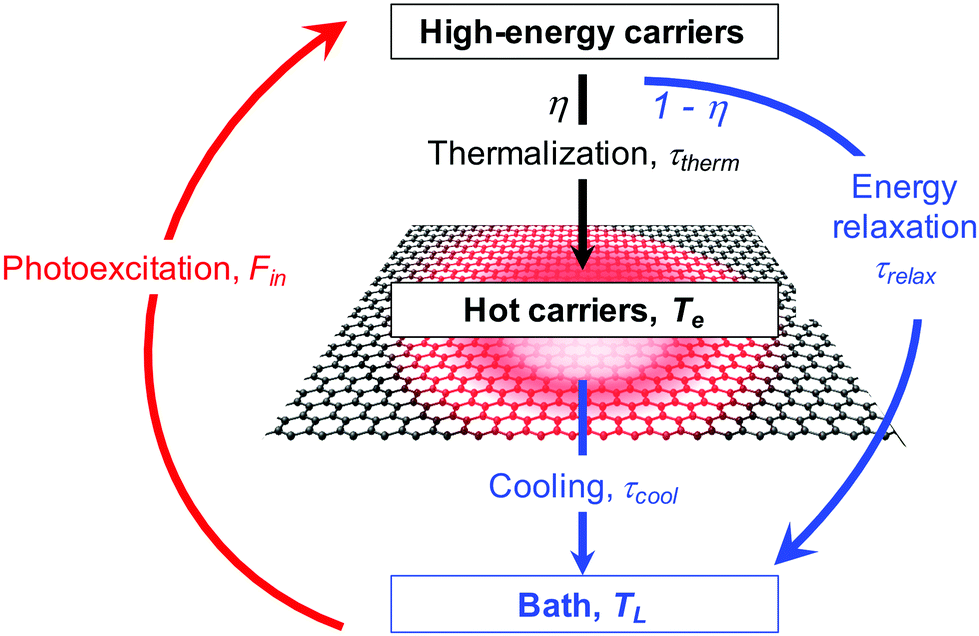
We distinguish two types of hot carriers, where in both cases charge carriers have an increased kinetic energy. We will use the term “high-energy charge carriers” for those that have an increased energy, yet do not form part of a thermalized carrier distribution. In this case, it is not possible to define a meaningful temperature, even if the carrier energy can be expressed in units of temperature. We will exclusively use the term “hot carriers” for those high-energy carriers that have thermalized with other charge carriers, thus forming a Fermi–Dirac distribution with an increased temperature – a hot-carrier distribution (see Fig. 1). In this case, the temperature of the electronic system Te is higher than the (equilibrium) temperature of the lattice TL.
 | ||
| Fig. 1 Illustration of heating–cooling dynamics of graphene carriers, where in the hot state the carrier distribution is characterized by an increased carrier temperature Te that is larger than the lattice temperature TL and a “hot” chemical potential μ that is smaller than the equilibrium chemical potential μeq. | ||
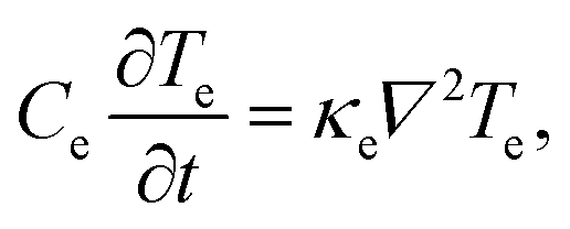
As a starting point for describing the relevant physics of hot carriers in graphene, we provide the thermoelectric equation describing the time evolution of the electronic temperature Te, assuming that the electron density remains constant over time t:
 | (1) |
![[Q with combining dot above]](https://www.rsc.org/images/entities/i_char_0051_0307.gif) ext, is the rate at which heat is added by external sources and removed via internal or external cooling channels, for example via electron–phonon collisions. The other two terms on the right-hand side are related to transport phenomena. The second term corresponds to Fourier's law of heat conduction, and contains the electronic part of the thermal conductivity κe. The third term describes the energy carried by the electric current density. In this term, Π is the local Peltier coefficient of the material, V is the local voltage, and
ext, is the rate at which heat is added by external sources and removed via internal or external cooling channels, for example via electron–phonon collisions. The other two terms on the right-hand side are related to transport phenomena. The second term corresponds to Fourier's law of heat conduction, and contains the electronic part of the thermal conductivity κe. The third term describes the energy carried by the electric current density. In this term, Π is the local Peltier coefficient of the material, V is the local voltage, and| J = σ(−∇V − S∇Te) | (2) |
This review is organized as follows: In section 2. Excitation, we will discuss different approaches for exciting graphene such that carriers are heated, followed by section 3. Energy dynamics on the thermalization and cooling dynamics of the electronic system. These two sections are mainly related to the term ext of eqn (1). In section 4. Conductivity, we will discuss the linear and nonlinear conductivity of hot carriers. We will then discuss transport phenomena in section 5. Transport, in particular diffusion and thermoelectric effects, related to the last two terms of eqn (1) and (2). We will then describe several applications enabled by hot carriers in section 6. Applications, followed by section 7. Discussion and outlook. Finally, we conclude with section 8. Conclusion. We also provide two boxes with background information: Box 1. Boltzmann theory and Box 2. Experimental techniques.
2 Excitation
In this section we will describe different ways of exciting graphene, such that hot carriers are created. We then discuss, from a macroscopic thermodynamic viewpoint, how a hot-carrier distribution is established after excitation.2.1 Heating sources
 | ||
| Fig. 2 Schematic illustrations of (a) thermal excitation, (b) electrical excitation, and (c) optical excitation. | ||
 | ||
| Fig. 3 Schematic illustration of the formation of hot carriers via photoexcitation, followed by thermalization of high-energy carriers. Since high-energy carriers can also directly relax to their environment, the branching ratio between these two processes determines the heating efficiency η. | ||
2.2 Macroscopic picture of carrier heating
ext = Pin − Γcool(Te − TL), where Pin is the absorbed power density of the external source, 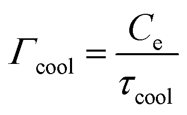 is the heat transfer coefficient in units W m−2 K−1, and τcool is the cooling time. The heat transfer coefficient describes the flow of heat out of the electronic system, for example through electron–phonon coupling. The thermoelectric equation, eqn (1), in this simple scenario reduces to
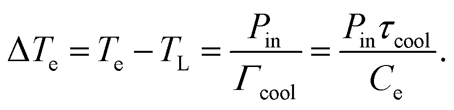 | (3) |
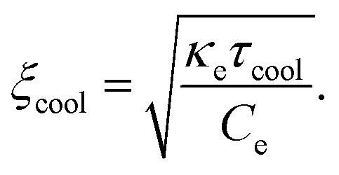
In order to increase the carrier temperature Te, for a given heating power density Pin, it is beneficial to operate with a small electronic heat capacity and a long cooling time. We will discuss the cooling dynamics in the next section. The electronic heat capacity, or specific heat, in two limiting cases – “doped” and “undoped” – is given by:29,30
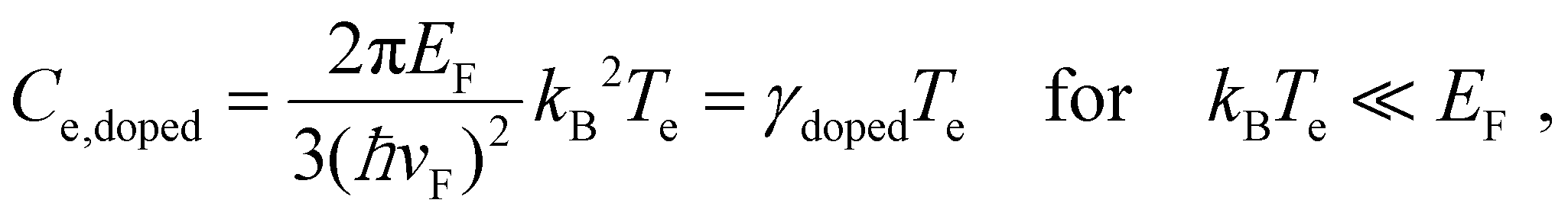 | (4) |
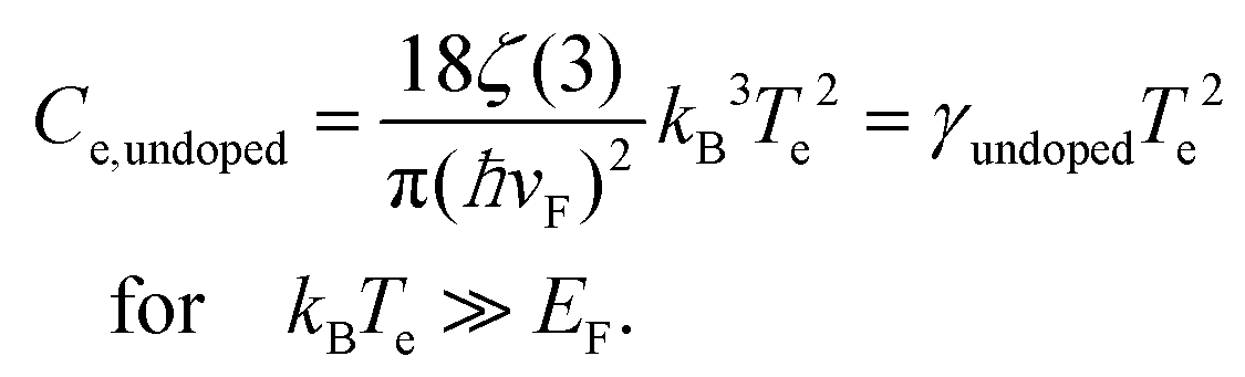 | (5) |
Here, ħ is the reduced Planck constant, vF the Fermi velocity, kB Boltzmann's constant, and ζ(3) ≃ 1.202. In the “doped” regime, the heat capacity decreases upon decreasing EF, as there are fewer electrons to share the energy. From the perspective of the specific heat, it is thus advantageous to operate at low Fermi energy, if the objective is to maximize the temperate increase ΔTe. Upon approaching the Dirac point, the EF-dependence drops out. In this case, ΔTe can be further maximized by operating at low temperatures. We note that graphene can reach record-low values of the electronic heat capacity, thus leading to large temperature rises for small excitation. Heat capacities as low as 2 × 10⁻⁹ J (m2 K)−1,31 and very recently even 1.2 × 10⁻¹¹ J (m2 K)−1,32 have been found using noise thermometry measurements.
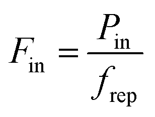 in order to calculate the peak increase in electron temperature ΔTe,peak. Here, frep is the repetition rate of the incident excitation, and the input fluence is the absorbed fluence (not the incident fluence). A lower repetition rate gives rise to a larger ΔTe,peak. In order to obtain the peak temperature, we solve the integral
 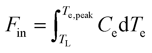 , and obtain the following sub-linear relationships between peak temperature and input fluence:
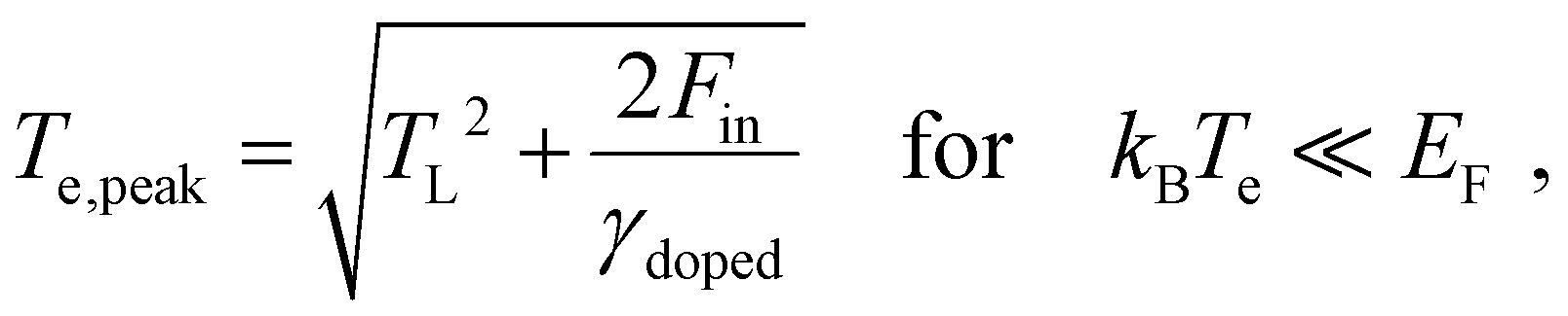 | (6) |
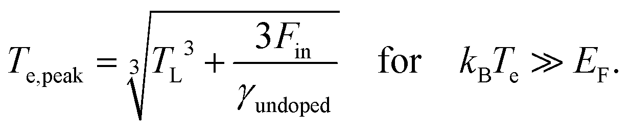 | (7) |
3 Energy dynamics
In this section, we describe the microscopic processes governing the energy dynamics of hot carriers. We start with a thermodynamic picture of carrier heating, followed by a description of the carrier–carrier interactions that lead to thermalization of the electronic system, after having absorbed a heating pulse, for example by photoexcitation. During these carrier–carrier interactions the total energy is conserved, and the electronic system typically evolves from a non-thermal to a thermal distribution with elevated carrier temperature. We then discuss the different interactions between carriers and other (quasi-)particles that lead to cooling of the hot-carrier system by damping of heat to a bath. Theoretical details on calculating these scattering events can be found in Box 1. We point out that the process we refer to as “thermalization” of the electronic system is sometimes referred to in literature as “internal thermalization”. This is in contrast to “external thermalization”, which refers to thermalization of the electronic system with the phonon system.
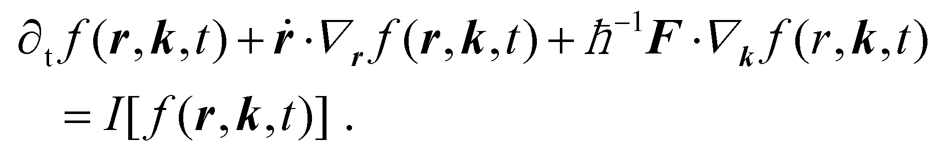
Box 1 Boltzmann theoryThe statistical modelling of thermodynamic out-of-equilibrium systems is usually performed by means of a “microscopic” Boltzmann equation, from which eqn (1) can be derived. The latter is commonly used to describe the kinetics of electrons in crystals in the so-called semiclassical regime,64,65 in which electronic states are described in terms of wave packets.66,67 When the length scales over which external electric (E) and magnetic (B) fields vary are much larger than the spread of wave packets themselves,66 the latter can be treated as point-like particles with well-defined position r (the “centre” of the wave packet) and wavevector k. Then, as usual in statistical mechanics, the properties of a large collection of particles can be determined by how they arrange in the phase space. The central object becomes the distribution function, f(r, k, t), which determines at every instant of time t the number of particles in an infinitesimal phase-space volume element centered around the point (r, k). In general, the number of particles therein changes over time. Firstly, when external forces are applied, after an infinitesimal time dt, the particles’ position and wavevector become r + ṙdt and k + Fdt/ħ, respectively.66,67 Here, F = −e(E + ṙ × B), while ṙ is the particle velocity which, barring Berry-curvature corrections,67 is equal to ħ−1∇kεk, where εk is their energy dispersion.The number of particles in a phase-space volume element changes over time also because of collisions, described via the collision integral64I[f(r, k, t)]. The collision integral accounts for all many-body scattering events a particle undergoes (against, e.g., impurities, phonons or other particles) that lead to a change of its wavevector k. After any such scattering event, a given particle transitions to a different phase-space volume element. Therefore, I[f(r, k, t)] is responsible for the time evolution of the occupation function due to collisions. The time evolution of the distribution function, accounting for both external forces and collisions, is described by the following equation:64,65 Eqn (1) can be derived by solving the equation above via the Chapman–Enskog method.68 Introducing the electron heat capacity and other transport coefficients, the resulting equation can be recast in the form of 1. Finally, we note that the equation above can be used to describe also the thermalization of non-equilibrium electrons (see section 3.1), not just their subsequent macroscopic cooling dynamics (eqn (1) – see also section 1). To describe the relaxation of non-thermal distribution, the equation above must however be solved numerically and yields a thermal distribution on time scales controlled by strength of the electron–electron collision integral. Once such distribution is reached, electron–electron collisions become ineffective (their collision integral vanishes for thermal distributions) and cooling proceeds via emission of phonons and can be effectively described viaeqn (1). |
3.1 Thermalization
Fermi–Dirac distribution. Microscopically, the electron temperature Te and chemical potential μ define the shape of the Fermi–Dirac distribution of a carrier system (see Fig. 1). This distribution describes the probability of finding an electron (e) or hole (h) with a certain energy ε, and is given by:
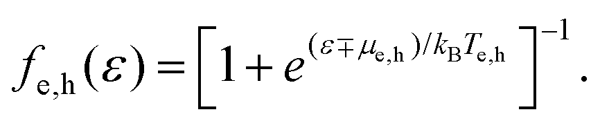 | (8) |
In equilibrium, the temperatures of the electrons in the conduction band and the holes in the valence band are equal, Te = Th, and so are their chemical potentials, μe = μh. The amount of kinetic energy density in units J m−2 in the electronic system is given by the sum of the energy density of electrons in the conduction band and holes in the valence band:  . These energies are given by:
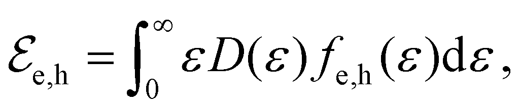 | (9) |
 , is excited by an absorbed energy density Fin, energy conservation dictates that
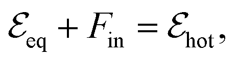 | (10) |
 that is characterized by “hot” Fermi–Dirac distributions with an increased carrier temperature. The electrons and holes thus have Fermi–Dirac distributions that are broadened. This broadening has been observed using time-resolved ARPES measurements, after pulsed optical heating37–39 (see Fig. 4a). Typically, it was found that within 150 fs the optically excited non-thermal distribution thermalizes.
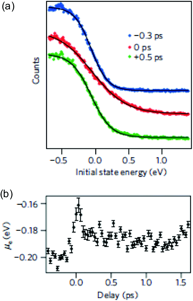 | ||
| Fig. 4 (a) Carrier distribution measured using time-resolved ARPES, at three different delay times: before (blue), during (red), and after (green) photoexcitation, clearly indicating a broadened (hot) distribution due to photoexcitation. The photon energy was ħω = 300 meV. (b) Extracted chemical potential from time-resolved ARPES measurements, as function of time delay after photoexcitation. Due to carrier heating, the chemical potential shifts towards the Dirac point. Panels (a) and (b) are adapted with permission from ref. 37 (Copyright 2013 Springer Nature). | ||
A broadening of the Fermi–Dirac distribution is accompanied by a decrease in the chemical potential, as dictated by conservation of the carrier density: ne − nh = const. The electron and hole carrier densities, ne and nh, respectively, are given by:
 | (11) |
This equation relates the variation in carrier density to the corresponding variation in temperature and, importantly, in chemical potential. Carrier density conservation dictates the following decrease of the chemical potential with carrier temperature, which in both doping regimes gives a decrease with increasing Te:
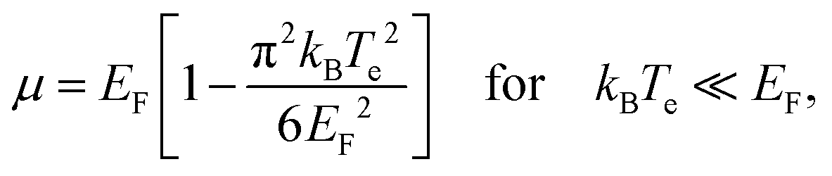 | (12) |
 | (13) |
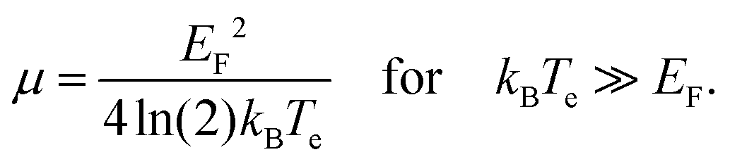
We note that the Fermi energy, which is defined at absolute zero temperature, is related to the carrier density via36
 | (14) |
Time-resolved ARPES studies (see Box 2) experimentally observed that the chemical potential indeed decreases upon carrier heating37 (see Fig. 4b). The decrease of the chemical potential upon carrier heating has several implications for transport properties (see section 4 on Conductivity and section 5 on Transport) and experimentally observable quantities using the techniques described in Box 2.
Box 2 Experimental techniquesSteady-state electrical and optical measurements. A measurement of the steady-state carrier temperature increase ΔTe can be obtained by radio-frequency Johnson noise measurements,21,22,104 taking advantage of the linear relation between the current noise spectrum and Te,105 or by detection and fitting with grey body radiation of the graphene hot-electron thermal emission.25,26 Another steady-state approach for the study of hot electrons is the excitation photomixing scheme.106Pump-probe. In ultrafast pump–probe experiments a first light pulse, called “pump”, generates high-energy charge carriers. The temporal evolution of these photoexcited carriers is subsequently detected by measuring the absorption, transmission or reflection of a second pulse, called “probe”.107–110 The relative temporal delay between the two pulses is controlled, such that the temporal resolution is determined by the duration of the ultrashort pulses. Tuning of the probe photon energy gives access to the energy distribution of the excited state. The photon energies used for the pump and probe can vary from the terahertz (ħω ∼ meV) to the UV (ħω ∼ eV). Time-resolved ARPES. In an angle-resolved photoemission spectroscopy (ARPES) experiment, high energy photons (ħω typically above 5 eV) impinge on a crystal in vacuum, ejecting electrons in free space, where their energies and exit angles are measured. These are related to the energy and crystal momentum of the electrons inside the sample. In the case of time-resolved ARPES, the sample is first excited by an ultrashort light pulse which generates high-energy charge carriers and subsequently the ARPES spectrum is measured with a second delayed high photon energy ultrashort pulse.111 Time-resolved photocurrent. In time-resolved photocurrent (trPC) experiments the sample is excited by two ultrashort laser pulses and the electrical response of the sample (photocurrent or photovoltage) is measured as a function of their delay. If the electrical response scales nonlinearly with the incident laser intensity, such as any hot-electron dominated photocurrent/photovoltage in graphene, the signal at zero/small delays will differ from the signal at large delays, and the recovery dynamics of the signal will reflect the time response of the sample.33,53,112–114 |
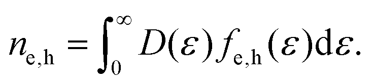
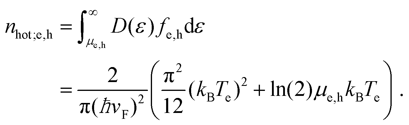
Hot-carrier density. It will be useful to consider the hot-carrier density nhot – the density of carriers with an energy larger than the chemical potential, given by†
 | (15) |
For intrinsic graphene with μe = μh = 0, this reduces to the thermal carrier density ntherm = (π/6)(kBTe/ħνF)2, often used for graphene under electrical heating.40,41 Whereas the carrier density ne − nh is conserved during thermalization, the hot-carrier density nhot increases. Several studies16,34,35,42–44 have discussed this effect quantitatively. In the next subsection, we will discuss the microscopic processes that are responsible for this.
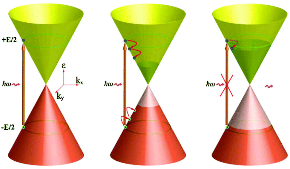
Intraband vs. interband thermalization. We now discuss the creation of an increased hot-carrier density in the two doping regimes. In the “doped” regime, with kBTe ≪ EF, only the carrier density of one band needs to be considered for energy and particle conservation. Thus, in the case of electron doping, it is enough to consider conservation of ne, because nh ≈ 0. The situation is different closer to the Dirac point, where kBTe ≫ EF. This is because the conserved quantity ne − nh allows for additional electron–hole pair creation across the bands, at least from a thermodynamic viewpoint. We illustrate this following ref. 35, in Fig. 5, where we show the initial Fermi–Dirac distribution directly after absorption of a heating pulse of absorbed power density Pin, yet before thermalization, and 300 fs later, when thermalization has occurred. These results are based on microscopic charge interactions (see Box 1 and next subsection), yet they provide a clear thermodynamic picture, with broadening of the distributions due to thermalization, i.e. an increased Te. They also confirm the decrease in chemical potential associated with thermalization. In the case where EF is initially far away from the Dirac point (EF = 0.4 eV), this broadening only affects the electrons in the conduction band. The density of holes in the valence band was basically zero before thermalization, and is still zero after thermalization. The density of electrons in the conduction band stays constant, whereas the density of hot electrons in the conduction band nhot,e has clearly increased. Therefore, thermalization in the case of large EF is referred to as intraband thermalization. In the case where EF is initially close to the Dirac point (EF = 0.05 eV), the broadening affects both electrons in the conduction band and holes in the valence band. Indeed, before thermalization there was a small density of holes in the valence band, whereas this density is increased after thermalization, as a result of charge and energy redistribution between the two bands. Also the density of electrons in the conduction band has increased. This means that – besides nhot – the density of interband electron–hole pairs, i.e. both ne and nh, has increased. Therefore, thermalization in the case of small EF is referred to as interband thermalization.
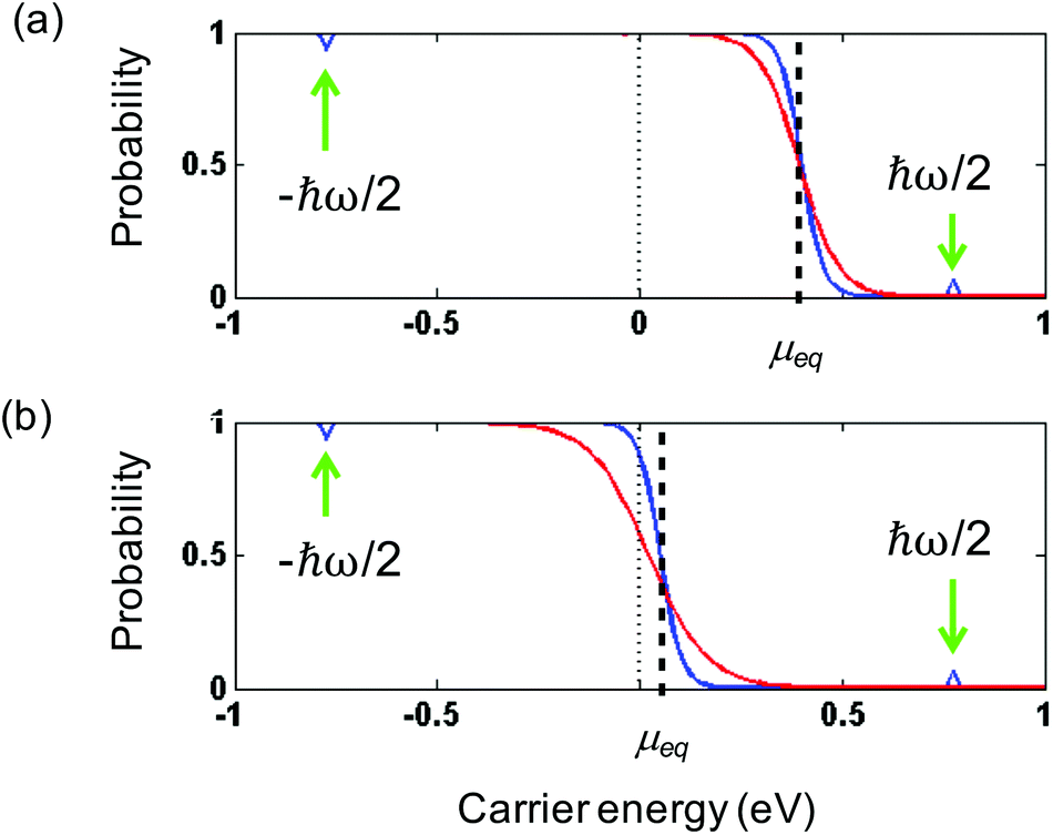 | ||
| Fig. 5 (a) Intraband thermalization after photoexcitation with ħω = 1.5 eV, for an initial chemical potential of 0.4 eV. The density of electrons in the conduction band ne is conserved, while Te increases. (b) Interband thermalization after photoexcitation, for an initial chemical potential of 0.05 eV. The density of electrons in the conduction band ne, and the density of holes in the valence band nh, increase, while Te = Th increases. In both cases, ne − nh is conserved, and nhot increases. These figures are based on microscopic simulations performed in ref. 35. | ||
The thermodynamic picture above suggests that the valence and conduction bands are thermalized with each other, such that the holes in the valence band and electrons in the conduction band have a common chemical potential and carrier temperature. The simulations of ref. 35 show that this is an excellent approximation when the system is examined 300 fs after excitation. At shorter timescales, this picture is not always very accurate. Indeed, several experimental studies with sub-50 fs time resolution have observed short-lived non-thermal distributions.39,45 A time-resolved ARPES study37 furthermore showed a situation where the carrier distribution consists of two separate Fermi–Dirac distributions – one for electrons and one for holes. This so-called “inverted” state was found to have a lifetime of ∼130 fs. Interestingly, the short-lived situation of two separate distributions was only observed in the case of interband photoexcitation (with photon energy ħω > 2EF), whereas intraband photoexcitation (with photon energy ħω < 2EF) directly led to a single, broadened Fermi–Dirac distribution for the valence and conduction bands. These results suggest the occurrence of a rich interplay of dynamical processes during carrier thermalization. We will discuss these dynamics in the following sections.
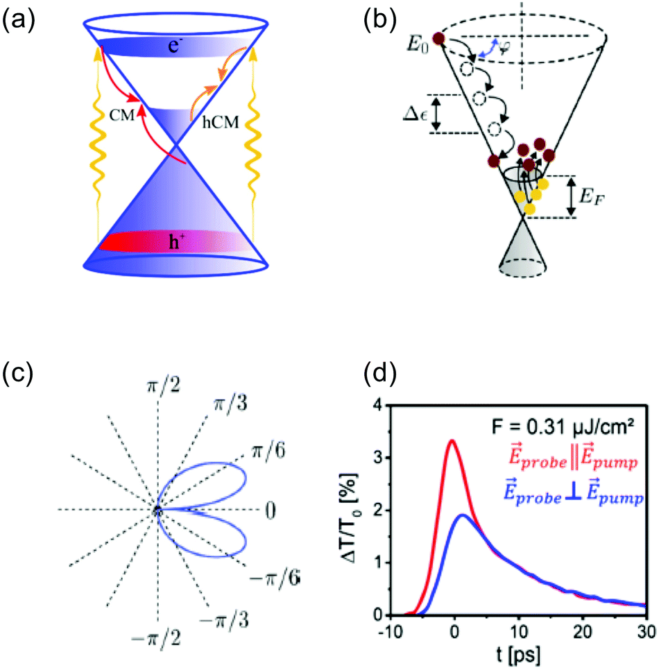 | ||
| Fig. 6 (a) Schematic illustration of thermalization via Coulomb-induced carrier–carrier scattering processes after photoexcitation. Here, “CM” indicates interband scattering processes (impact ionization and Auger recombination) that can lead to the creation of multiple electron–hole pairs per absorbed photon – carrier multiplication. Similarly, “hCM” indicates intraband scattering processes that can lead to the creation of multiple hot electrons per absorbed photon – hot-carrier multiplication. (b) Schematic illustration of the details of thermalization via intraband carrier–carrier scattering (impact excitation), where one initial high-energy electron leads the creation of multiple hot carriers, i.e. hot-carrier multiplication. In each relaxation step, the initial electron transfer an average mount of energy Δε ≃ EF to an electron in the Fermi sea. The angle φ indicates the change in momentum of the initial electron. (c) Calculation of the angular distribution of intraband impact excitation scattering for the initial high-energy electron, indicating near-collinear scattering. (d) Experimental observation of anisotropic carrier distribution through pump–probe spectroscopy, with pump and probe polarizations parallel (red) or perpendicular (blue). The photon energy was ħ = 88 meV. Panel (a) is adapted with permission from ref. 46; panels (b) and (c) are adapted with permission from ref. 42 (Copyright 2013 American Physical Society); panel (d) is adapted with permission from ref. 47 (Copyright 2016 American Physical Society). | ||
Hot-carrier multiplication. In order to examine thermalization via carrier–carrier scattering more closely, we first discuss the situation where high-energy carriers have been created, typically by photoexcitation of graphene with a photon energy ħω > 2EF (see Fig. 6b). This creates carriers with an energy around ε = ħω/2 above the Dirac point. In the “doped” case, where kBTe ≪ EF, these initial high-energy carriers lose kinetic energy through intraband, inelastic scattering with carriers in the Fermi sea, which gain kinetic energy. Thus, secondary hot carriers are created. This is the process of impact excitation. The amount of energy Δε that is exchanged between an initial high-energy carrier and a carrier in the Fermi sea follows a distribution function that peaks around EF.42 Therefore, a single (primary) high-energy carrier can create multiple secondary hot carriers during its cascade, transferring an average amount of Δε ≈ EF to each secondary hot carrier. This corresponds to the creation of multiple hot carriers per absorbed photon, gradually increasing nhot. The occurrence of hot-carrier multiplication was predicted and addressed quantitatively using optical-pump terahertz probe measurements with varying pump photon energy,34,42 and using time-resolved ARPES measurements.43 It was furthermore experimentally confirmed when Wu et al. succeeded in electrically collecting multiple hot-carriers per absorbed photon in a photodetector system.44 The occurrence of hot-carrier multiplication shows that carrier heating in graphene is an exceptionally efficient process that can be exploited for various applications (see section 6).
Carrier multiplication. While hot-carrier multiplication can occur in the “doped” regime, where intraband thermalization dominates, “real” carrier multiplication can occur close to the Dirac point, where kBTe ≫ EF. In this regime interband thermalization occurs, and multiple free carriers can be created per absorbed photon. Winzer et al. showed that there is a competition between the interband processes of impact ionization and Auger recombination, and predicted the occurrence of carrier multiplication for relatively weak photoexcitation.50 Carrier multiplication was observed experimentally in ref. 51, although no unambiguous results have been presented (yet) showing the electrical collection of multiple electron–hole pairs per absorbed photon. We note that the thermodynamic regimes of interband thermalization and intraband thermalization correspond to the regimes where carrier multiplication and hot-carrier multiplication, respectively, can occur under certain circumstances35,46 (see Fig. 6a). In semiconductors, the creation of multiple carriers per absorbed photon is very attractive, as it enables efficient photodection and energy harvesting beyond the Shockley–Queisser limit.52 In graphene, hot-carrier multiplication is arguably more crucial, as there are several ways to exploit the additionally created hot carriers, as we will discuss in section 6.
Effect of photon energy and power. For impact excitation, a higher photon energy leads to a higher energy of the primarily excited high-energy carriers. Because the average energy exchange per scattering event Δε is ∼EF, a higher photon energy leads to a larger number of scattering events during the relaxation cascade, and therefore to the creation of a larger number of secondary hot carriers per absorbed photon, as shown experimentally.34 Thermodynamically, this corresponds to a larger increase in Te per absorbed photon. Interestingly, for a given absorbed fluence Fin, the temperature increase is roughly independent of photon energy. This is because Fin = ħωnħω, where nħω is the absorbed photon density. This means that for a fixed Fin, an increase in photon energy corresponds to a decrease in photon density, such that the overall heating, in principle, does not depend on photon energy for a given absorbed fluence. Indeed, a constant thermal photocurrent was measured over a broad wavelength range.53 We note that a larger photon energy can lead to a longer duration of the thermalization cascade,34 which means that competing energy relaxation processes become more important, leading to a lower heating efficiency η for higher photon energies.
So far, we have considered the case of interband photoexcitation, with ħω > 2EF. For intraband excitation, with ħω < 2EF, the thermalization dynamics are in many ways very similar. Intraband excitation leads to acceleration of free carriers that gain kinetic energy. These carriers then distribute their energy with the other carriers in the Fermi sea. Indeed, the creation of a thermalized hot state after intraband photoexcitation was observed, even within 30 fs (ref. 37) (see also Fig. 4a). In agreement with this observation of ultrafast thermalization, there are several experimental indications, for example using mid-infrared or terahertz light,54–56 that intraband photoexcitation leads to efficient carrier heating, at least within the same band.
When keeping the photon energy fixed, while increasing the incident power, or fluence, the heating efficiency η typically decreases. Indeed, both the carrier multiplication efficiency50 and hot-carrier multiplication efficiency57 were found to decrease with increasing Pin, and time-resolved optical experiments that require relatively large absorbed fluences (typically above 10–100 μJ cm−2), such as time-resolved photoluminescence30 and time-resolved ARPES37,38 typically found relatively low heating efficiencies. Microscopically, this is related to the relatively large density of initial high-energy carriers, and relatively high carrier temperature that is being established during thermalization. This slows down the thermalization process, thus making τheat longer. This means that the heating efficiency η becomes smaller, due to competing energy relaxation processes for high-energy carriers, with relaxation time τrelax (see Fig. 3). Furthermore, once thermalization has occurred, at sufficiently high carrier temperatures, efficient cooling can occur, for example via optical phonon emission (see section 3.2.1).
Momentum exchange. Carrier–carrier scattering events do not only lead to exchange of energy; also carrier momentum is modified (see angle φ in Fig. 6b). As discussed in several theoretical and experimental works,42,45,47,49,50,58 carrier–carrier scattering occurs preferentially in the near-collinear direction, due to the kinematic constraints of carrier–carrier scattering processes (see Fig. 6c). Purely collinear scattering, however, is suppressed, because due to their relativistic band dispersion, electrons and holes all share the same group velocity, while backscattering is strongly suppressed because of their chirality. In low dimensionality, the result is a diverging duration of collisions for collinear particles.59 The preferred near-collinear scattering means that photoexcitation with linear polarization leads to an anisotropic distribution in momentum space, which lasts longer than the interaction time with the photons (see Fig. 6d). In the case of excitation with a photon energy above the optical phonon energy, the distribution becomes isotropic in ∼150 fs.47,58 This is attributed to phonon-mediated non-collinear carrier scattering. However, in the case of excitation with a photon energy below the optical phonon energy, scattering occurs purely through carrier–carrier interactions, and the anisotropy was found to survive for picoseconds at 20 K. This effect can survive up to room temperature.47,60
Controlling carrier–carrier scattering. We already saw that changing the Fermi energy and the incident photon energy changes the thermalization cascade. However, it is also possible to control the intrinsic carrier–carrier scattering events. For example, the Coulomb interaction strength decreases with temperature, leading to a longer carrier–carrier scattering time at lower temperature, as observed experimentally.61 Furthermore, one can control carrier–carrier scattering by proximity screening, as demonstrated recently using a high-quality graphene sample with a nearby metal.62 Finally, the application of a magnetic field will lead to less efficient carrier–carrier scattering.63
3.2. Carrier cooling
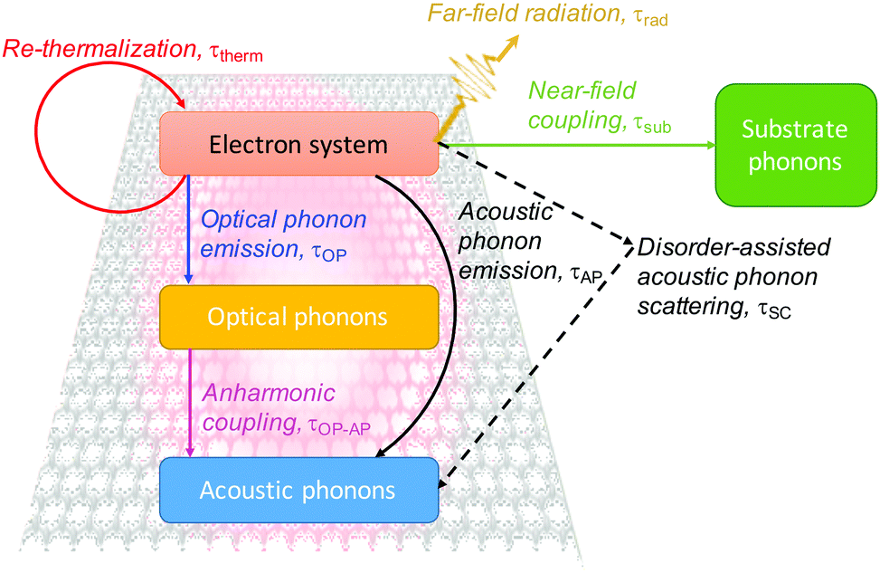 | ||
| Fig. 7 Schematic overview of hot-carrier cooling mechanisms. | ||
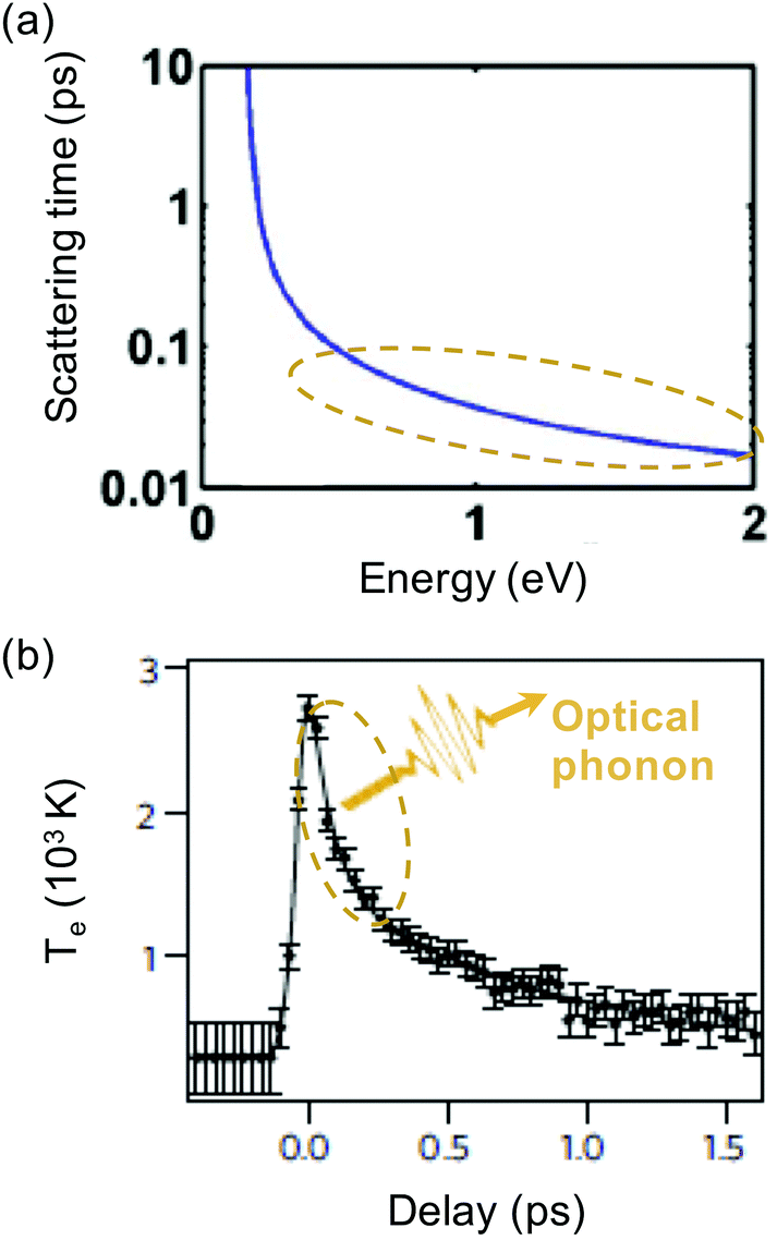 | ||
| Fig. 8 (a) Calculation of scattering time between a charge carrier with a certain energy and optical phonons, τOP. (b) Experimental measurement of cooling dynamics using time-resolved ARPES, showing an initial fast decay (∼100 fs) due to optical phonon emission. The slower tail is either ascribed to optical-to-acoustic phonon conversion (hot-phonon bottleneck) or to disorder-assisted acoustic phonon cooling. Panel (a) is adapted with permission from ref. 74 (Copyright 2010 American Institute of Physics); panel (b) is adapted with permission from ref. 37 (Copyright 2013 Springer Nature). | ||
Time-resolved studies using relatively strong excitation, leading to many high-energy carriers, typically observed ultrafast (few hundred fs) emission of so-called strongly-coupled optical phonons (SCOPs), cf. ref. 74–77, in agreement with the calculations of ref. 74 shown in Fig. 8a. As a result, fast thermalization occurs not only within the electronic system, yet also between the electronic system and the optical-phonon system. This leads to charge carriers having a temperature similar to the temperature of optical phonons, while the acoustic phonon temperature is much lower. This was also observed in electronic transport studies at high electric field.25,78 Typically, in these studies, bi-exponential cooling dynamics were observed (see Fig. 8b): sub-picosecond decay due to coupling to optical phonons (τOP), followed by few-picosecond decay that was attributed to cooling of the hot optical phonons to acoustic phonons (τOP–AP), as the hot phonons are not able to cool fast enough, and re-heat the electronic system. This effect of the hot optical phonons is sometimes referred to as the hot-phonon bottleneck for carrier cooling. The optical phonon lifetime τOP–AP has been measured independently, for example through time-resolved Raman measurements, yielding values ranging from 1.2 to 2.55 ps.30,74,79–81
For carriers with lower energy, (ε + μ) < EOP, the timescale of optical phonon emission increases exponentially (see Fig. 8a). Therefore, in the case of relatively weak excitation, or after strong excitation, followed by fast cooling to optical phonons, once Te is smaller than ∼1000 K, cooling via optical phonons was thought to be rather inefficient.33 In this case, there would not be enough high-energy carriers to emit optical phonons. Indeed, several experimental studies showed a temporary thermal decoupling between the electronic system and the phonon system, allowing the electronic system to heat up efficiently, before it cools down via phonons.82 Recently however,83,84 it was shown that optical phonons can still play an important role in hot-carrier cooling even for carrier distributions with a temperature close to room temperature. This is based on the idea that (at least at room temperature and above) there is a significant fraction of carriers in the tail of the Fermi–Dirac distribution with a kinetic energy that is large enough to couple to optical phonons. Once these high-energy carriers have relaxed by emitting optical phonons, re-thermalization of the electronic system occurs. This leads to “newly excited” carriers with high enough energy to relax by emitting optical phonons. These processes of optical phonon emission and re-thermalization occur simultaneously. Thus, cooling occurs by the combination of optical phonon emission and continuous re-thermalization of the carrier system. A numerical simulation based on this intrinsic cooling mechanism was shown to be consistent with temperature-dependent cooling dynamics obtained with optical-pump THz-probe measurements.83 More recently, it was shown that this cooling mechanisms leads to bi-exponential decay, with a sub-picosecond initial decay related to direct coupling to optical phonons, and a few-picosecond decay due to the hot-phonon bottleneck.84 This study showed that a larger peak temperature and smaller EF typically give rise to slower cooling dynamics for this cooling channel. For graphene where alternative cooling channels (see below) are suppressed, this cooling channel ultimately determines the intrinsic limit of the hot-carrier lifetime of high-quality graphene (with a mobility >10![[thin space (1/6-em)]](https://www.rsc.org/images/entities/char_2009.gif) 000 cm2 V−1 s−1) at room temperature.84
000 cm2 V−1 s−1) at room temperature.84
 | ||
| Fig. 9 (a) Schematic illustration of cooling via acoustic phonons without (left) and with (right) disorder, where the presence of disorder speeds up the emission of acoustic phonons, also known as “supercollision cooling”.85 (b) Experimental measurements of cooling dynamics using time-resolved photocurrent microscopy, together with calculations using disorder-assisted acoustic phonon cooling. Panels (a) and (b) are adapted with permission from ref. 33 (Copyright 2013 Springer Nature). | ||
000 cm2 V−1 s−1 at room temperature.96,97 It is also a naturally hyperbolic material, with hyperbolic phonon polaritons occurring in its two Reststrahlen bands, which are the spectral intervals between the longitudinal (LO) and transverse (TO) optical phonon frequencies.98 Owing to these two spectral regions with hyperbolic phonon polaritons, two optoelectronic experiments have shown that cooling of hot carriers in hBN-encapsulated graphene occurs via out-of-plane coupling to hyperbolic phonon polaritons in hBN.22,91,92 These studies showed that a higher peak temperature and a smaller EF typically give rise to slower cooling dynamics for super-Planckian cooling to hyperbolic substrate phonon modes (see Fig. 10b).
 | ||
| Fig. 10 (a) Schematic illustration of cooling of hot carriers in graphene (red dots) via hyperbolic phonon polaritons in hBN (red lines) via near-field radiation. (b) Experimental measurements of cooling dynamics using time-resolved photocurrent microscopy, showing faster cooling for lower EF, the opposite trend compared to disorder-assisted cooling. Panel (a) is adapted with permission from ref. 91 (Copyright 2017 American Physical Society); panel (b) is adapted with permission from ref. 92 (Copyright 2018 Springer Nature). | ||
We briefly mention alternative cooling channels. Coupling to graphene plasmons could play a role in the early stages of the energy cascade,100 and was suggested to explain the short-lived inverted state observed in ref. 37. Experimental signatures of this cooling mechanism were observed recently.101 Furthermore, hot-carrier photoluminescence – Planck radiation from the hot-carrier system – has been shown to occur.30 However, this process is inefficient: it gives rise to a Γcool of ∼10 W m−2 K−1,92 corresponding to a τcool of ∼10 ns. A theoretical proposal suggested that exploiting plasmonic near-field effects between neighboring graphene nano-islands could speed radiative heat transfer up to the femtosecond regime.102 A final cooling mechanism that was identified corresponds to resonant dissipation from individual atomic defects in graphene, as observed in ref. 103. Finally, we note that under certain external conditions – beyond those that create defects or modify the Fermi energy or peak/lattice temperature – the carrier dynamics can be altered. Most notably, the application of a magnetic was shown to lead to significantly slower dynamics.63
4 Conductivity
The conductivity σ governs both the electrical transport and the optical properties of graphene.115 In the following we will discuss the linear and nonlinear frequency- and temperature-dependent conductivities.4.1 Linear conductivity
There is nowadays a large amount of theoretical115–123 and experimental124,125,126,127–130 works dealing with the linear frequency-dependent optical conductivity of graphene σ(ω). Here we will focus on how the interband and intraband transitions of graphene depend on carrier temperature. Typically, for frequencies up to a few THz the intraband conductivity dominates, while for higher frequencies both contributions can play a role. Note that for graphene on a substrate the absorbance (in SI units and normal incidence) is related to σ(ω) by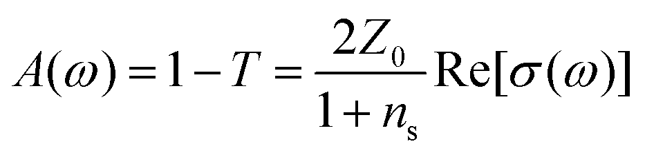 , where
  is the vacuum impedance, ns the substrate's refractive index and T is the transmission.130,131 This means that σ(ω) determines the number of photogenerated hot electrons, as it determines the optical absorption, and it's directly related to Joule heating as it determines the resistance of a graphene sheet (see section 2).
 | (16) |
For large enough photon energies, when ħω ≫ 2|μ| and ħω ≫ 4kBTe, interband transitions dominate graphene's absorbance and eqn (16) reduces to σ(ω)inter = σ0 = e2/(4ħ), which thus becomes independent of frequency.124,125,133 For this value of the sheet conductivity the absorbance for isolated (suspended) graphene (ns = 1) depends only on elementary constants 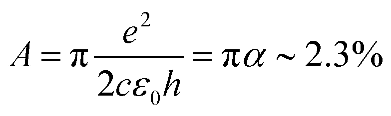 . Note that
  is the fine structure constant. The same “universal conductivity” can be obtained from the Fermi golden rule for two-dimensional Dirac fermions.124
For large energies, graphene's band structure deviates from linear dispersion, and excitonic effects at the saddle point singularity at ∼5 eV lead to increased absorption.121,127 Although theory predicts that the approximation of a linear dispersion should hold only for relatively small values of the incident photon energy (ħω < 1 eV),124 experiments observed very small deviations from the universal value of the absorbance A ∼ 2.3% for photon energies up to ħω = 1.5–2 eV.124,127 For higher photon energies, the conductivity deviates significantly from the universal value.
Another key aspect of σ(ω)inter is that the value 2μ, which defines the crossing from intraband to interband transitions, can be tuned by doping and external gate voltages,134 leading to the possibility of designing gate-tuneable optical modulators.135 According to eqn (16), due to heat-induced broadening of the Fermi–Dirac distribution and the accompanying shift in the chemical potential μ, interband absorption can either increase (for ħω < 2EF) or decrease (for ħω > 2EF), as shown in Fig. 11.
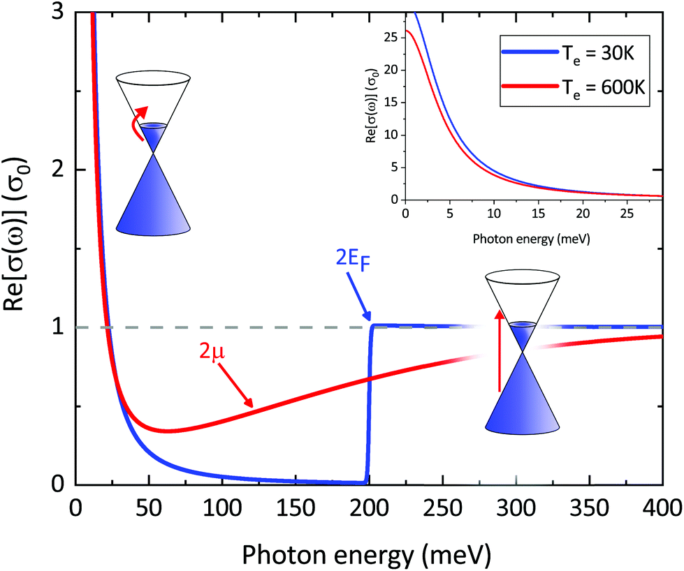 | ||
| Fig. 11 Real part of graphene's frequency-dependent linear optical conductivity in units of σ0 based on eqn (16) for interband transitions and (18) for intraband transitions (Drude model) with fixed momentum relaxation time τ = 1 ps and different values of Te and μ: Te = 3 K and μ = 0.1 eV (blue curve), Te = 600 K and μ = 0.057 eV (red curve). Note that for interband transitions σ at Te = 600 K can either decrease or increase compared to the value at Te = 30 K close to ħω = 0.2 eV. For intraband transitions (inset) σ decreases (negative photoconductivity) as expected from the Drude model in the limit of large doping (Te < TF). | ||
 | (17) |
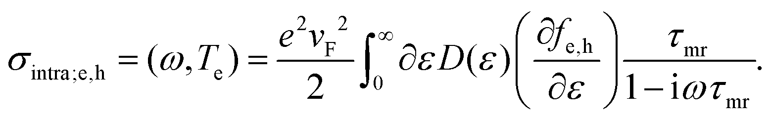
There are three main approaches that have been used to understand how this intraband conductivity changes upon carrier heating, which is less straightforward than in the case of interband transitions. Experimentally, this issue has been addressed in particular using optical pump – terahertz probe studies, cf. ref. 34, 35, 57 and 136–139. We will now describe the three approaches, where we note that they are not mutually exclusive.
Drude weight. In the first approach, the temperature dependence is fully captured by the so-called Drude weight:131,137
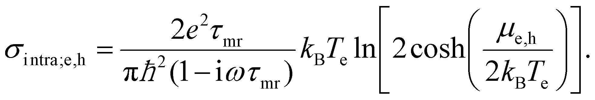 | (18) |
This result comes from considering spectral weight conservation,137 which is related to the Thomas–Reiche–Kuhn sum rule for light–matter interaction.140 For the graphene conductivity, this sum rule indicates that the broadening of the interband conductivity (see previous subsection, and Fig. 18) implies that, in the “doped” regime, the spectrally integrated weight of interband transitions increases. In the “undoped” regime, the integrated interband weight decreases. Spectral weight conservation then dictates that the spectrally integrated weight of intraband transitions should decrease (increase) for the “doped” (“undoped”) case. Note that the Drude weight for graphene is different compared to conventional semiconductors or metals.127,128 This approach predicts that if kBTe ≪ EF, namely for weak heating and large doping, the hot-carrier conductivity is smaller than the equilibrium conductivity (negative photoconductivity), which is in agreement with several experiments34,35,57,136–139 (see inset Fig. 11). Furthermore, it explains the experimental observation of an increase in conductivity, i.e. positive photoconductivity, close to the Dirac point (where the ratio Te/TF is large), as observed in ref. 35, 57, 137 and 139. This approach, however, does not take into account that momentum scattering can depend on Fermi energy and/or carrier temperature. Furthermore, the Drude weight predicts positive photoconductivity at high fluence, which is in contradiction with experiments. In ref. 137, the dependence of umr on Te was inserted phenomenologically, assuming Te = TL and momentum relaxation dominated by phonon scattering.
Sommerfeld expansion. In ref. 34, the microscopic intraband conductivity of eqn (17) was calculated in the Sommerfeld expansion regime, where the ratio Te/TF is small. Here, the energy-dependence of the momentum relaxation time was taken into account, under the realistic assumption that it is dominated by long-range Coulomb scattering with impurities. This corresponds to a momentum relaxation time that typically increases linearly with carrier energy,123 and is typically the channel that limits charge mobility at room temperature in substrate-supported graphene. This approach correctly gives the negative photoconductivity for EF away from the Dirac point, as observed experimentally.34,35,57,136–139 However, it can not be used close to the Dirac point, as the conditions for the Sommerfeld expansion are not met.
Full microscopic approach including dynamical screening. Finally, in ref. 35, the microscopic intraband conductivity eqn (17) was calculated explicitly, including the energy-dependent momentum relaxation time, governed by long-range Coulomb scattering with impurities. Dynamical screening in the random-phase approximation was taken into account in the calculation of τmr. This approach gives positive photoconductivity close to the Dirac point and negative photoconductivity away from the Dirac point, in agreement with experiments.35,57,137,139 According to ref. 35, the positive photoconductivity close to the Dirac point is the result of the increase in the charge carrier density (interband thermalization with possible carrier multiplication). Away from the Dirac point (where the charge carrier density does not increase, as intraband thermalization occurs), the conductivity is negative, because the heated carrier distribution leads to a decrease in screening of the Coulomb interaction with impurities.35
 | (19) |
 | (20) |
 | ||
| Fig. 12 Sketch of the SA process in the case of interband transitions driven by hot-electron broadening of the Fermi–Dirac distribution and Pauli blocking. Reprinted with permission from ref. 154 (Copyright 2009 Wiley). | ||
 | (21) |
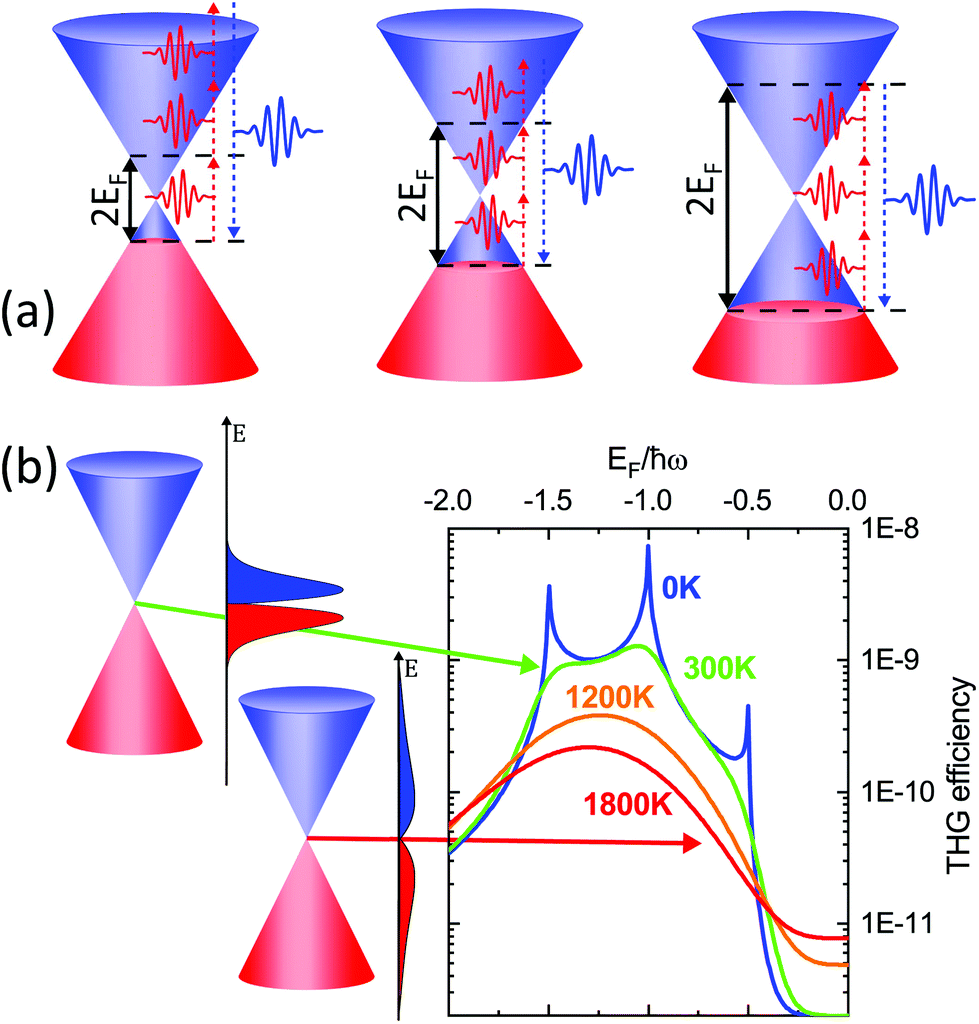 | ||
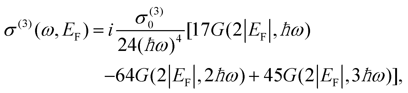
| Fig. 13 (a) THG in graphene is enhanced at specific values of EF corresponding to one-, two- and three-photon transitions within the Dirac cone. (b) The increase of Te affects the nonlinear conversion efficiency by broadening the electron distribution. The graph shows the THG efficiency, defined as I3ω/Iω, for ħω = 500 meV and a peak power density of ∼230 MW cm−2. | ||
Recently, HHG (Fig. 14a) with extremely high field-conversion efficiencies of 10−3, 10−4 and 10−5 for third, fifth and seventh harmonics, respectively, was demonstrated at room temperature using doped single-layer graphene.56 The result was successfully interpreted based on a nonlinearity mechanism that does not rely on coherent electron motion. Rather, the THz nonlinearity was understood from a purely thermodynamic picture of the THz response of doped graphene. In this thermodynamic picture,56,173 hot carriers play a central role, because the intense nonlinear response of graphene is due to the combination of the THz-induced carrier heating that reduces the THz conductivity,54 together with the ultrafast heating and cooling dynamics of hot electrons (Fig. 14b). We have discussed the effect of carrier heat on the THz intraband conductivity in section 4.1 and the details of the heating–cooling dynamics in section 3. The nonlinearity arises simply because THz absorption leads to carrier heating, which leads to negative THz photoconductivity, i.e. reduced THz absorption. This effect was discussed in detail in ref. 54. Since heating is highly efficient, this mechanism leads to very high nonlinearity coefficients. The heating–cooling dynamics play a crucial role in observing the THz harmonics created by a multicycle incident THz pulse, as detailed in ref. 56 and 173.
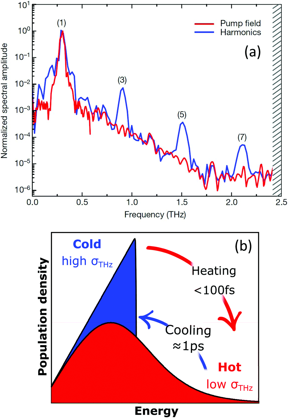 | ||
| Fig. 14 (a) THz high-harmonic generation from single layer graphene. (b) Excitation in the THz corresponds to an oscillating period of the electric field of ∼1 ps, thus much longer than carrier–carrier scattering and comparable to the cooling time. For this reason, the nonlinear optical response of graphene in this frequency range is driven by incoherent thermodynamic effects arising from the strong temperature dependence of the sheet optical conductivity σ(ω) (inset). Panel (a) is adapted with permission from ref. 56 (Copyright 2018 Springer Nature). | ||
In the future, THz nonlinear optics with graphene could offer a rich playground for on-chip signal processing174 and for the study of the hydrodynamic regime (see 5.1.4) with Dirac fermions.175
5 Transport
In this section, we address transport properties related to hot carriers. We first discuss intrinsic properties such as hot-carrier diffusion and thermoelectric effects. Subsequently, we discuss interlayer phenomena, involving transport of graphene hot carriers to a neighboring material.5.1 Diffusion
 | (22) |
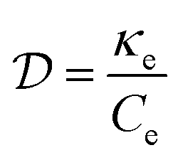 , typically given in units of cm2 s−1. Since hot charge carriers are transporting the electronic heat, the thermal conductivity κe and charge conductivity σ are directly related in the diffusive regime, namely through the Wiedemann–Franz relation:
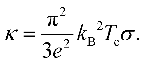 | (23) |
It can be shown (see ref. 176) that this gives a simple relation between diffusivity and charge mobility μcharge, which is the same result that can be obtained using the Einstein relation:
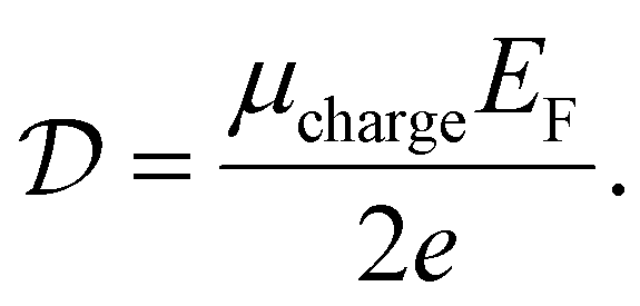 | (24) |
This predicts that the electronic heat diffusivity in graphene at room temperature has a value of 100–5000 cm2 s−1, for typical EF up to 0.2 eV and mobilities varying from a few thousand cm2 V−1 s−1 for CVD graphene up to 50000 cm2 V−1 s−1 for hBN-encapsulated graphene. Microscopic simulations predicted a diffusivity of 360 cm2 s−1.177 The diffusivity of graphene was first studied experimentally using all-optical spatiotemporal scanning,178 which found a short-lived initial  of 5500–11000 cm2 s−1, followed by a value on the order of 250 cm2 s−1. Recently, a spatio-temporal thermoelectric scanning microscopy experiment on hBN-encapsulated graphene found a value of ∼2000 cm2 s−1.176 This value is in agreement with the measured electrical charge mobility μcharge of ∼40000 cm2 V−1 s−1 for their sample, thus being in accordance with the Wiedemann–Franz and Einstein relations.
 | (25) |
For EF ≫ kBTe, and owing to the Wiedemann–Franz relation, this can be written as:
 | (26) |
A special hydrodynamic charge transport regime exists very close to the Dirac point: the Dirac fluid. Here, the Wiedemann–Franz relation breaks down, and electronic heat can travel unimpeded, as electrons and holes travel together along a thermal gradient.99 This typically occurs very close to the Dirac point, requiring cryogenic temperatures and ultra-clean samples. However in the case of elevated Te and in the absence of electron–phonon thermalization, it can also be observed further away from the Dirac point, as demonstrated experimentally in ref. 176. In this study, increased diffusivities of hot carriers were found in the first few hundred femtoseconds after photoexcitation with  up to 70000 cm2 s−1 and thermal conductivities above 10000 W m−1 K−1. This transport occurs in the hydrodynamic time window before momentum relaxation occurs (∼350 fs in their case), whereas carrier have already thermalized through carrier–carrier scattering.
5.2 Thermoelectric effects
 | (27) |
We note that this formula, which is based on Boltzmann theory (see Box 1), is derived using the Sommerfeld expansion and is thus only valid in the degenerate limit kBTe ≪ EF, which is the case for most metals and doped graphene. In practice, SMott can be calculated from the measurement of electrical conductivity of graphene at varying EF, which is conveniently achieved using a gate voltage.
Since 2009, the Mott relation has been experimentally verified several times in graphene.18,19,190–193 In these experiments, the Seebeck coefficient is typically measured using microfabricated heaters to create a temperature gradient while measuring the thermally induced voltage across the device (see inset Fig. 15). The first measurements of the Seebeck effect in graphene revealed a sizable thermopower value, reaching ∼80 μV K−1 close to the Dirac point at room temperature. The sign of the thermopower changes across the Dirac point, as the majority carrier density switches between holes and electrons. At high carrier density, the thermopower is proportional to  and increases linearly with Te, as predicted by the Mott formula. Since the latter depends on the energy derivative of the conductivity, the thermopower strongly depends on the scattering mechanism governing the electrical conductivity σ. Of particular importance is how the momentum relaxation time τmr depends on carrier energy ε. As Hwang et al.194 pointed out, long-range scattering by screened charged impurities appears to be the dominant scattering mechanism in most graphene samples at room temperature. Deviations from the Mott formula were observed close to the Dirac point and at high temperature, where the Sommerfeld expansion is no longer valid. These discrepancies, as well as the nonlinear temperature dependence of S observed in clean graphene devices,195,196 can be explained theoretically by employing an effective medium theory and by considering the energy-dependence of τmr for different momentum scattering mechanisms.194
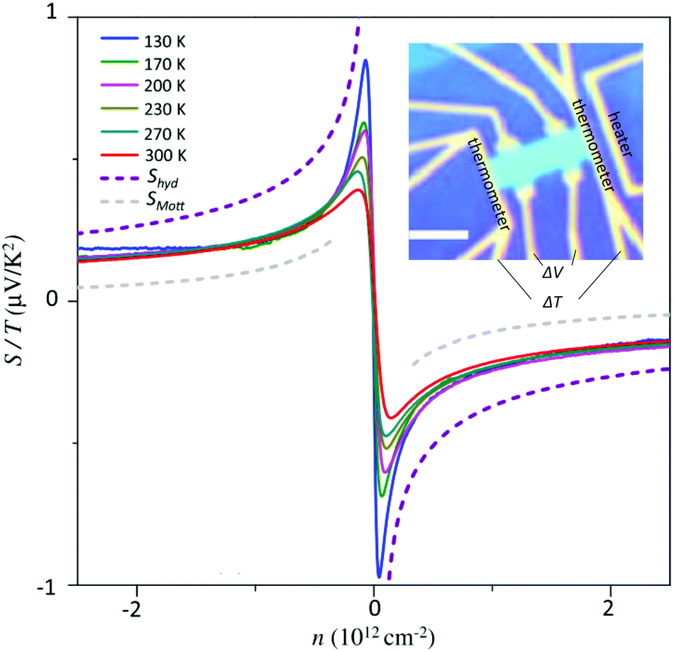 | ||
| Fig. 15 Measured S/Te as a function of charge carrier density n at different temperatures. The grey and purple curves represent SMott/Te and Shyd/Te, respectively. The inset shows a typical device used to measure S, where the scale bar corresponds to 2 μm. The figure is adapted with permission from ref. 190 (Copyright 2016 American Physical Society). | ||
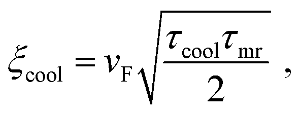
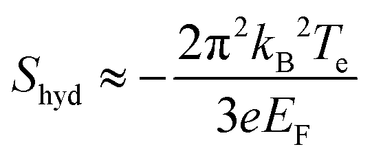
The situation is quite different in clean graphene samples with ultra-high mobility. As discussed in section 5.1.4, inelastic electron–electron scattering can become the dominant scattering process in clean graphene, and the resulting hydrodynamic behavior of charge carriers can lead to a violation of the Mott formula. This effect was first investigated theoretically in the context of hydrodynamic transport in Dirac fluids.197,198 It was predicted that in a purely hydrodynamic regime, the Seebeck coefficient is the entropy transported per charge of the carrier, which in the degenerate regime gives
 | (28) |
Ghahari et al. provided evidence of hydrodynamic thermoelectric transport in hBN-encapsulated graphene samples with extremely low disorder.190 At high temperature, the measured thermopower surpasses the calculated SMott, approaching the predicted Shyd (see Fig. 15). This result was explained by considering the inelastic scattering between carriers, as well as the one between carriers and optical phonons. According to a recent theoretical prediction,199 this enhancement of the Seebeck coefficient in the hydrodynamic regime, combined with the low κhyd in the Fermi-liquid regime should give rise to significant improvement of the heat-to-work conversion efficiency of thermoelectric devices.
 | (29) |
 | ||
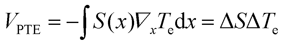
| Fig. 16 (a) Schematic representing the generation of a PTE voltage in a graphene p–n junction. Light absorbed at the junction between regions with different Seebeck coefficients (S1 and S2) increases the electronic temperature by ΔTe and generates a photovoltage VPTE. (b) Photovoltage as a function of back (VBG) and top (VTG) gate forming a p–n junction. The six-fold change of polarity of VPTE is characteristic of the PTE effect.82,179 Grey dashed lines represent lines of high resistance taken from transport measurements, while the white dashed line indicates where the carrier density in the two regions is equal. Panel (a) is adapted with permission from ref. 200 and panel (b) is reproduced from ref. 82 with permission from AAAS. | ||
The PTE effect was first observed at interfaces of single layer and bilayer graphene203 and graphene p–n junctions.82 By varying EF on both side of the junction, Gabor et al.82 showed that photovoltage exhibits a six-fold pattern (see Fig. 16b), which is a hallmark of the PTE effect. Indeed, Song et al.179 predicted that the non-monotonic behaviour of S(EF) shown in Fig. 15 should lead to multiple sign changes of VPTE (when S1 = S2 or EF ∼ 0 in both regions), in stark contrast with the single sign reversal expected for the photovoltaic effect. The PTE effect has also been shown to dominate the photoresponse of unbiased graphene-metal junctions114,204,205 and supported-suspended graphene interfaces.206 We note however that the photovoltaic and photo-bolometric effect can become predominant in biased graphene devices.206 In section 6.1, we discuss in more details the performance of photodetectors based on the PTE and photo-bolometric effects.
= (Π2 − Π1)I. This effect has been observed at graphene-metal junctions20,207 and around geometrical constrictions,208,209 typically using scanning thermal microscopy. These results, in combination with the record high thermoelectric power factor σS2 measured in clean graphene devices,196 demonstrate the advantage of using graphene as an active thermoelectric cooler. We also note that according to recent theoretical studies, the Thomson effect becomes stronger in the hydrodynamic regime199 and can lead to cooling of the Fermi liquid.210
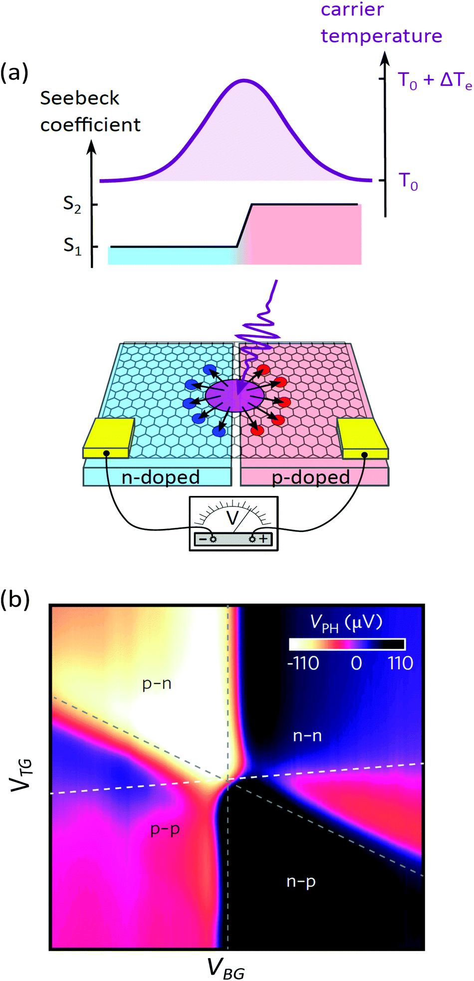
Finally, in the presence of an out-of-plane magnetic field Bz (with respect to the 2D graphene plane), hot carriers diffusing under ΔT are deflected by a Lorentz force, producing a transverse voltage Vy. This thermomagnetic effect analogous to the Hall effect is called the Nernst effect and is quantified by the Nernst coefficient
 | (30) |
5.3 Interlayer transport
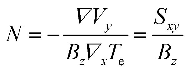
Recent advances in the layer-by-layer assembly of 2D materials has led to the birth of a very active field of research on the so-called van der Waals heterostructures (vdWH).212–214 Interfacing graphene with other bulk or 2D materials has emerged as a powerful way to engineer material properties of hybrid systems. This is perhaps best exemplified by the recent discovery of anomalous superconductivity in twisted bilayer graphene.215 These heterostructures also provide the ability to control and exploit the properties of hot carriers in graphene. For instance, as discussed in section 3.2.3, encapsulating graphene using hBN gives rise to a new cooling pathway mediated by hyperbolic phonon polaritons in hBN.92 In addition to influencing the heat transfer, these heterostructures can enable the transport of carriers in the out-of-plane direction (see Fig. 17a). This interlayer charge transport generally takes place across g/X heterojunctions, where g denotes graphene and X represents a semiconducting or insulating material, and involves transport mechanisms that are drastically different from intralayer transport. Indeed, inside individual layers, transport is generally diffusive and carried out by the delocalized carriers of the band structure. In the out-of-plane direction, carriers are localized on each layer and their interlayer transport is controlled by the potential energy barrier Φ formed at the heterojunction. Thus, charge transport between layers typically entails processes such as tunneling and thermionic emission. | ||
| Fig. 17 (a) Schematic of interlayer transport and intralayer thermalization of photoexcited carriers in a g/hBN/g heterostructure. (b) Band diagram of a graphene heterostructure illustrating various interlayer transport mechanisms. The yellow shaded area in the hot-carrier distribution n(E) represents the carriers with an energy larger than the barrier Φ that can generate thermionic emission. Panel (a) is reproduced with permission from ref. 216 (Copyright 2016 Springer Nature). | ||
Recently, several vertical transport models have been proposed that take into account the linear dispersion relation of graphene.223,225–228 While these models deviate from the classic Richardson's and Fowler–Nordheim laws, the aforementioned exponential behaviours hold true. These transport mechanisms have been observed in g/Si Schottky junctions229,230 and in several graphene heterostructures where layers of hBN or TMDs are employed as potential barriers.231–234 In these devices, the crystal lattices of the component layers were not aligned, so the in-plane momentum of the carriers was not conserved during transport. Indeed, the presence of disorder and phonons can lead to relaxation of the momentum conservation condition. Remarkably, by aligning the crystallographic orientation of the layers, momentum and energy conservation leads to resonant tunneling. It was experimentally shown that this can result in a strong negative differential resistance that persists up to room temperature.235,236 This coherent interlayer transport can be modelled using more advanced techniques such as ab initio simulations,224 and nonequilibrium Green's function237 and transfer Hamiltonian238 formalisms.
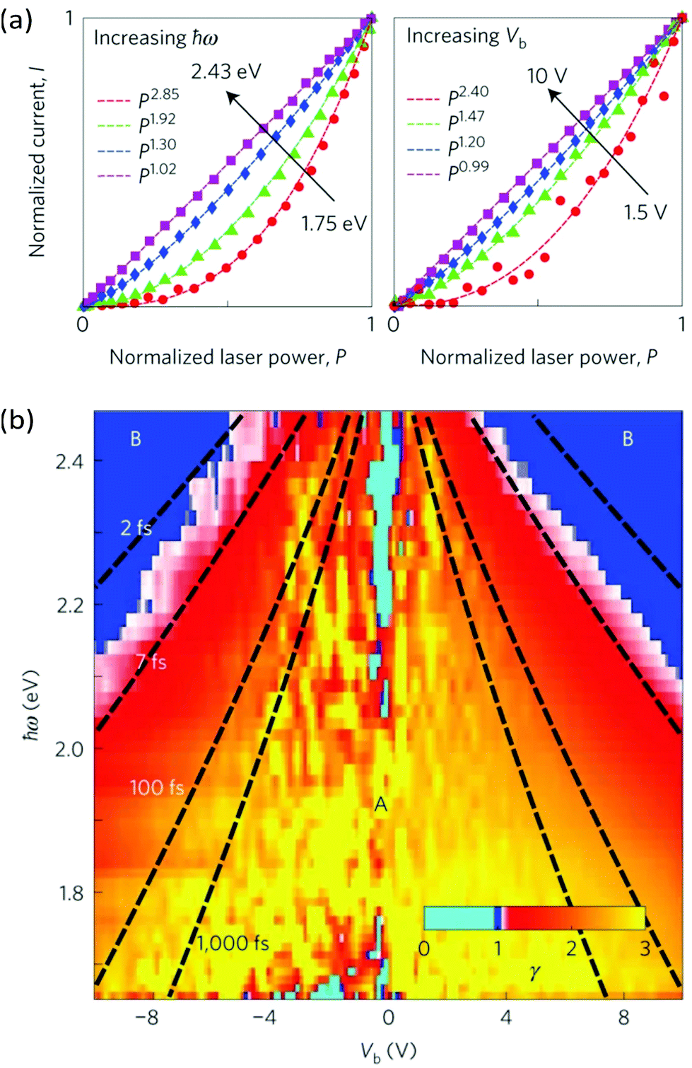 | ||
| Fig. 18 Competing interlayer transport processes of photoexcited carriers in a g/hBN/g heterostructure. (a) Photocurrent I as a function of excitation laser power P, at constant interlayer bias Vb but increasing photon energies ħω (left panel), and at constant photon energy ħω but increasing bias (right panel). The data are fitted with a power law I ∼ Pγ. (b) Colour map of γ as a function of Vb and ħω. The black dashed lines correspond to different tunnelling times. Regions A (γ > 1) and B (γ ∼ 1) indicates where the interlayer current is dominated by photo-thermionic emission and photon-assisted tunneling, respectively. This figure is reproduced with permission from ref. 216 (Copyright 2016 Springer Nature). | ||
By increasing the excitation photon energy or the interlayer bias voltage on their g/hBN/g devices, Ma et al.216 detected a second interlayer transport mechanism which they identified as photon-assisted tunneling, a process related to internal photoemission.243 In this transport regime, photoexcited carriers in graphene tunnel through the hBN barrier before they thermalize with other carriers. This competition between PTI emission and photon-assisted tunneling provides a way to manipulate electron thermalization in graphene and to estimate the thermalization time of carriers (τheat ∼ 10 fs, see Fig. 18b). Both PTI emission and photon-assisted tunneling were also shown to contribute to the photocurrent generation in g/SiC Schottky junctions. By modelling the dependence of the photocurrent on the laser pulse duration, a tunneling time as short as ∼0.3 fs was extracted, which offers exciting perspectives for applications in ultrafast electronics.244
The dynamics of interlayer charge transport in g/TMD junctions have recently been the focus of several optical pump–probe studies.245–247 While all studies have observed the generation of photocarriers in the TMD layer after sub-bandgap photon energies, its origin is still debated. Yuan et al.246 suggested that in addition to hot carrier injection, charges in graphene can be photoexcited directly to the adjacent TMD layer via charge transfer states resulting from strong interfacial electronic coupling. In contrast, Chen et al.247 performed similar measurements and proposed that photoexcited charges in graphene are transferred to the TMD layer after carrier intraband scattering but before electron–hole interband thermalization. In a recent study combining ultrafast terahertz and visible probes, Fu et al.245 observed a superlinear dependence on the pump fluence for excitation below the TMD bandgap, consistent with PTI emission observed in photocurrent experiments.
6 Applications
The exceptional properties of graphene, such as its broadband absorption and ultrafast photoresponse, have led to several promising applications in photonics and optoelectronics. Indeed, graphene-based devices display many desirable features, such as high-speed operation, wide spectral response, gate tunability and compatibility with silicon photonics and CMOS platforms. Here, we focus on photonic and optoelectronic devices where hot-carrier effects play a central role, in particular photodetectors, nonlinear optical devices and light emitters.6.1 Photodetectors
Over the past decade, significant efforts have been dedicated to the development of graphene-based photodetectors, as illustrated by the many review articles published on this topic.12,13,258–262 Graphene photodetectors can convert absorbed photons into an electrical signal through various mechanisms, including mainly the photo-thermoelectric (PTE), photo-bolometric (PB), and photovoltaic (PV) effects. While the latter is based on photoexcited carriers, PTE and PB mechanisms are driven by the excess carrier temperature ΔTe. As discussed in section 5.2.2, PTE photodetectors produce a photovoltage (or photocurrent) when hot carriers are generated at the junction between regions with different Seebeck coefficients. A hot-carrier bolometer detects incident radiation by measuring the light-induced temperature increase of the electronic bath.263 This is typically achieved by measuring changes in the temperature-dependent resistance (dR/dT) of the device or by measuring thermal noise.Both PTE and PB detectors take advantage of properties of hot carriers in graphene. As explained in section 3.1, light-induced carrier heating in graphene is efficient because the electron–phonon coupling is weak compared to the strong electron–electron interactions, possibly even leading to the generation of multiple hot carriers per incident photon. Due to the record small heat capacity of graphene, this photogenerated heat gives rise to a substantial increase in Te, which in turns generates a large PB and PTE response. Finally, carrier cooling occurs on a picosecond timescale, enabling high-speed photodetection. These unique thermal properties, combined with the broadband photon absorption of graphene, make graphene-based photodetectors highly promising for many applications. Below we concentrate on long-wavelength and ultrafast photodetectors whose performances are often on par with, or even better than, the best commercially available devices, while offering specific benefits.
One general approach to increase the sensitivity of graphene photodetectors is to optimize the photodetection mechanism which converts the excess carrier temperature ΔTe into an electrical signal. In PTE detectors, this conversion is governed by the Seebeck coefficient S, which can be maximized by tuning the chemical potential close to Dirac point but outside the electron–hole puddle regime (see Fig. 15. For this reason, clean and electrically-tunable graphene p–n junctions are often used to increase the responsivity of PTE detectors.55,82,266,267 In the case of PB devices, the relatively weak dR/dT of graphene (<1%/K)268 limits the sensitivity of photodetectors based on the readout of the electrical resistance. One way to solve this issue is to artificially increase dR/dT, for instance, by nanostructuring graphene269 or creating a bandgap in bilayer graphene.270 Another strategy is to employ a different scheme to read out ΔTe, for example by measuring the Johnson noise of graphene104,271 or the switching current of graphene-based Josephson junctions.265
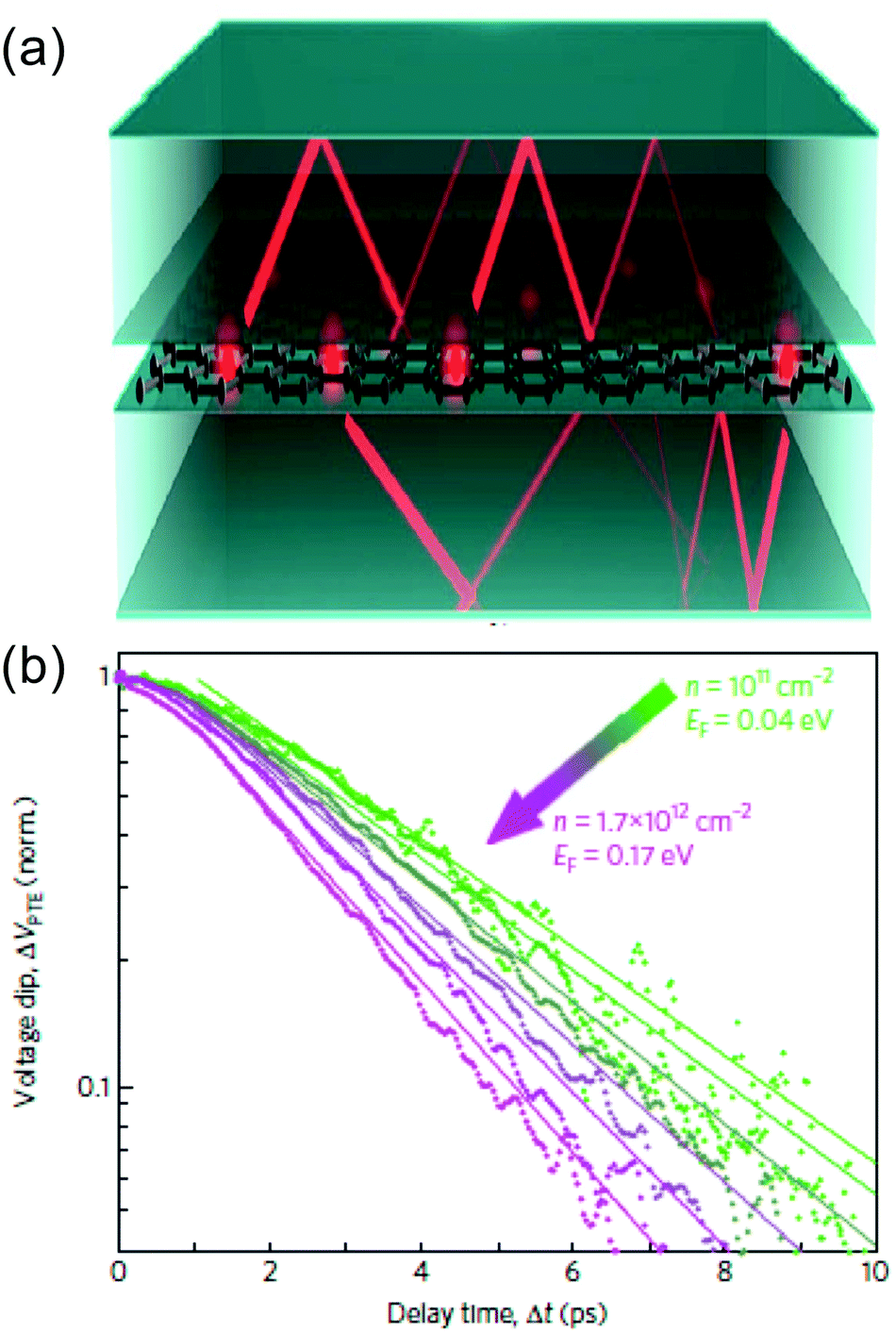
A second common strategy to increase the sensitivity of both PTE and PB photodetectors is to increase ΔTe by enhancing the interaction of graphene with the incident light. This can be accomplished by integrating photonic structures, such as optical cavities, waveguides and photonic crystals, with the photodetector.272 For THz and mid-IR photodetectors, antennas with various geometries (see Fig. 19a) have been used to compensate for the mismatch between the large area of the incoming radiation and the small photoactive area of the detector.55,264,273–277 At GHz frequencies, microwave resonators (see Fig. 19b) have been used to couple light with 99% efficiency to graphene bolometers.32,265 Light–matter interactions can also be enhanced by taking advantage of the polaritonic resonances of graphene or neighbouring materials,272 such as plasmon-polariton in graphene an nearby metal nanostructures, or hyperbolic phonon-polaritons in hBN. The quasiparticles, which are at the center of a rich field of research,278 can tightly confine light in the photodetector, resulting in an increased ΔTe. This approach has been shown to enhance the response of many hot-carrier photodetectors, from the visible to THz spectral range.279–282 Finally, another avenue to increase ΔTe is to reduce the heat transfer coefficient of hot carriers in graphene. For example, this can be accomplished by operating the photodetectors at low temperature181 or by suspending the graphene layer.206 However, while this increases the responsivity of the detector, the longer cooling time leads to a longer photoresponse time.
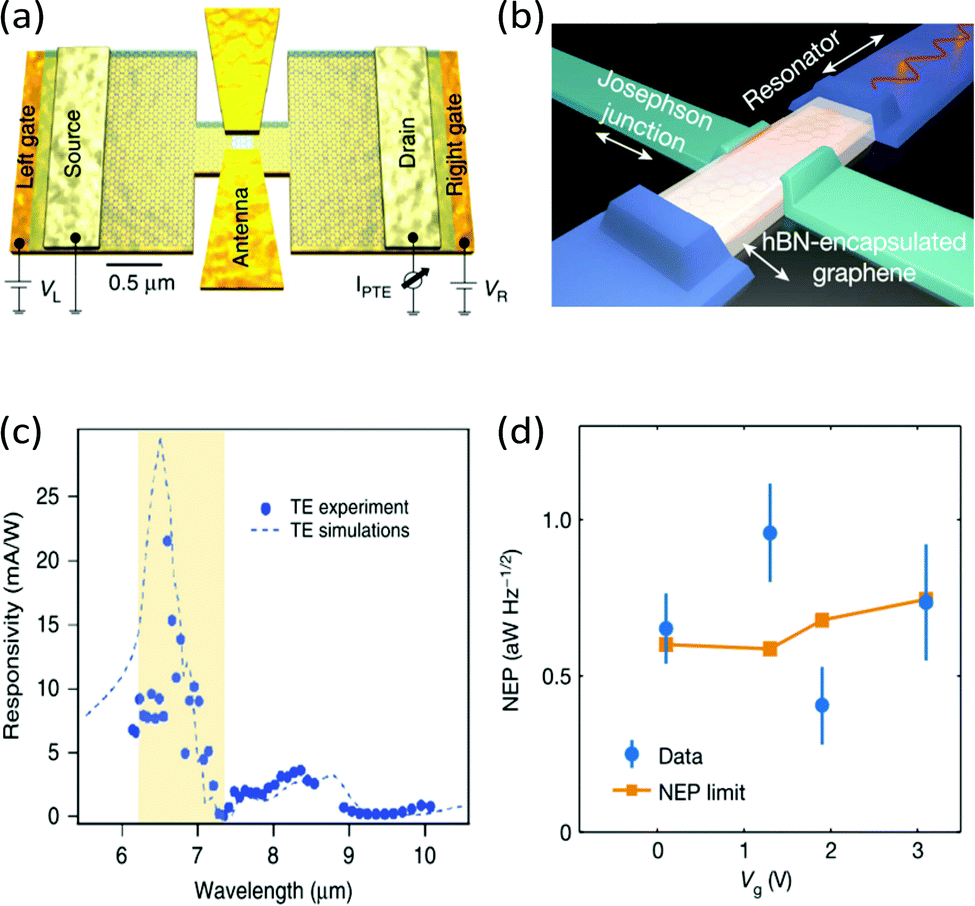 | ||
| Fig. 19 (a) Schematic of a mid-IR photodetector consisting of a hBN-encapsulated, H-shaped graphene p–n junction with a bow-tie antenna. (b) Schematic of a graphene-based Josephson junction microwave bolometer. The bolometer is embedded in a half-wave resonator to allow DC readout (green) of the Josephson junction and microwave excitation (blue). (c) Measured (dots) and calculated (dashed line) responsivity spectrum of the photodetector shown in (a) for TE-polarization. The yellow shaded region corresponds to the Reststrahlen band of hBN where light absorption in graphene is enhanced due to the propagation hyperbolic phonon-polaritons. (d) NEP measured (blue dots) using the device shown in (b) and the thermal fluctuation limit of the NEP (orange). Panels (a) and (c) are reproduced from ref. 264 and panels (b) and (d) are reproduced with permission from ref. 265 (Copyright 2020 Springer Nature). | ||
Several of these sensitivity-enhancement strategies have been combined, in order to create high-performance long-wavelength photodetectors that operate at room-temperature. In the mid-IR region, where light absorption in graphene is particularly low due to Pauli blocking, Castilla et al.264 reported a PTE photodetectors based on clean a hBN-encapsulated graphene p–n junction with a responsivity of ∼27 mA W−1 (see Fig. 19c), an NEP of ∼80 pW Hz−0.5 and a fast rise time 17 ns. They achieved this by designing a plasmonic antenna efficiently coupled to hyperbolic phonon-polaritons in hBN, which in turn concentrate mid-IR light onto the p–n junction. Safaei et al.280 demonstrated a plasmon-assisted PTE photodetector using partially nanopatterned graphene, which exhibits a NEP of only ∼7 pW Hz−0.5 with a response time of ∼100 ns. In the THz range, PTE photodetectors made of hBN-encapsulated graphene coupled to metallic antennas have displayed a very low NEP (∼80 pW Hz−0.5) and very fast response (∼3 ns), in particular compared with other THz detectors at room temperature.55,283 Finally, two recent studies32,265 on microwave bolometers based on superconductor–graphene–superconductor junctions reported an NEP below 1 aW Hz−0.5 (see Fig. 19d), down to 30 zW Hz−0.5, and a response time of 200 ns, when operating in the mK temperature range. All these performance parameters are comparable or superior to other existing long-wavelength detectors, demonstrating the potential of hot-carrier photodetectors for a wide range of applications.
High-speed telecom photodetectors. Graphene photodetectors also hold great potential for high-speed photodetection at telecom wavelengths, which is the key process in optical receivers. The latter are a critical part of optical communication systems as they often determine the overall system performance.284 While most dominant technologies rely on the PV effect in semiconductors like Ge, high-speed graphene photodetectors exploit the ultrafast dynamics of photoexcited carriers in graphene to rapidly convert an optical signal into an electrical one. In the case of PTE and PB photodetectors, an electrical signal can be generated in less than 50 fs (ref. 53) as photoexcited carriers transfer their energy to the electronic bath, leading to the formation of a hot carrier distribution. When the light is turned off, hot carriers cool back to the lattice temperature with a characteristic time τcool ∼ 1–2 ps. This process determines the intrinsic bandwidth of the PTE and PB detectors. Early studies revealed that the intrinsic bandwidth of graphene photodetectors can exceed 260 GHz,112,113,285 indicating their potential for data communication applications. We note, however, that the bandwidth of actual devices can be limited by extrinsic factors, including the RC time constant of the device or the bandwidth of the amplifier.
Several chip-integrated graphene-based photodetectors similar to the one shown in Fig. 20a have been reported during the past few years.242,286–297 In these devices, light in the waveguide is evanescently coupled to the graphene layer. Compared to free-space illumination, the long interaction length between the guided mode and graphene increases the optical absorption well above the usual value of a few percent. Almost 100% optical absorption can be achieved with an interaction length >40 μm. PB photodetectors with a bandwidth larger than 110 GHz and a responsivity of up to ∼0.5 A W−1 have been demonstrated.295,296 However, since these photodetectors operate with a bias voltage, they suffer from a large (>100 μA) dark current, resulting in high shot noise and increased power consumption.
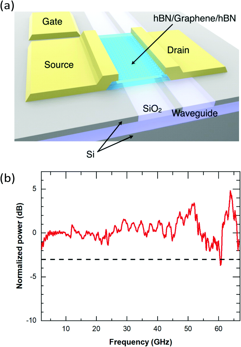 | ||
| Fig. 20 (a) Schematic of a high-speed photodetector consisting of a hBN-encapsulated graphene layer evanescently coupled to light in the buried silicon waveguide. (b) Spectral response of a PTE photodetector measured up to 67 GHz. The dashed line indicates the 3 dB drop of the photoresponse. No roll off is observed in the in the frequency range of the measurement. Panel (a) is reproduced with permission from ref. 286 (Copyright 2015 American Chemical Society) and panel (b) is reproduced with permission from ref. 287 (Copyright 2020 American Chemical Society). | ||
In contrast, PTE detectors operate at zero-bias in either current or voltage mode, while maintaining a large photodetection bandwidth and responsivity. Like most conventional photodetectors, the current mode requires a transimpedance amplifier, whereas the voltage configuration can operate using a simpler and less costly voltage amplifier. Responsivities of up to ∼0.4 A W−1 and 12 V W−1 have been reported for PTE photodetectors. These devices typically display a bandwidth larger than 40 GHz (ref. 286, 289, 290 and 292) and the highest to date surpasses 67 GHz (setup-limited, see Fig. 20b).287 Finally, we note that graphene heterostructures, which are based on interlayer transport mechanisms (see section 5.3), are also promising for high-speed photodetection as they can potentially improve the responsivity while maintaining low dark current and high bandwidth.242,294 Ultimately, improving the large-scale fabrication298 and design13 of graphene-based photodetectors could open the door to faster and more power-efficient receivers in tele- and datacom modules.
6.2 Nonlinear optical devices
Owing to its strong and gate-tuneable nonlinear optical response148,149 and its ease of integration in photonic devices such as fibers,153 waveguides152 and micro-resonators,300,301 graphene has been widely explored for applications in nonlinear optics. Notable examples are saturable absorbers and other optical modulators, frequency converters and sensors.15,155,259,302,303A notable example of all-optical modulation is saturable absorption (see section 4.1.3), a nonlinear and non-parametric third-order process that has been extensively used for passive mode-locking of ultrafast lasers (Fig. 21a).155,303 Graphene SAs have been used to mode-lock both solid-state305–307 and fibre lasers154,308–312 at 800 nm,307 1 μm,311 1.5 μm,154,308 2 μm (ref. 306 and 311) wavelengths and for passive synchronization of separate laser cavities operating at different wavelengths.313 Saturable absorption based on σintra (see section 4) is possible also at THz frequencies.173,314 Graphene SAs have enabled the generation of ultrashort pulses with <70 fs duration307 and lasers with GHz repetition rate.301,310 Several other approaches have been implemented for the realization of graphene-based all-optical amplitude modulators. With a graphene-clad microfiber (Fig. 21b) Li et al.299 demonstrated all-optical modulation with 38% modulation depth and ∼2 ps switching time while Liu et al.315 showed CW all-optical modulation with modulation depth of 5 dB and 13 dB using single- and bi-layer graphene respectively. An all-optical modulator based on a Mach–Zehnder interferometer reached a modulation depth >50% while maintaining an optical transmission through the device of 19%.316 All-optical modulation can be obtained also with graphene transferred on photonic crystal cavities owing to a combination of light-induced resonance-tuning and SA.317 Finally, Ono et al.318 showed ultrafast all-optical modulation with modulation speed of 260 fs and extinction ratio of 3.5 dB using only 3.5 fJ of switching energy in a graphene-loaded deep-subwavelength plasmonic waveguide.
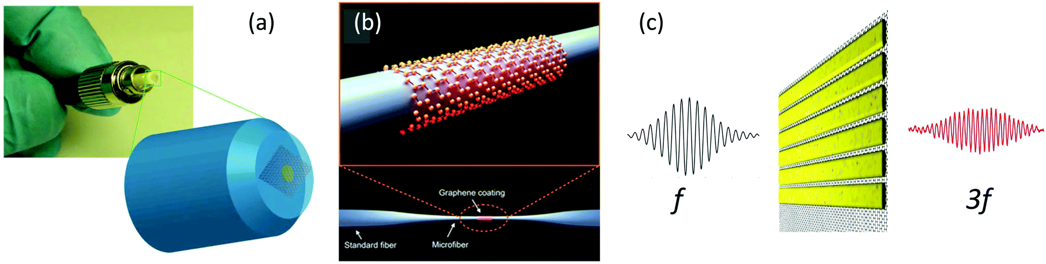 | ||
| Fig. 21 Examples of graphene-based nonlinear devices enabled by hot electrons: (a) graphene based SA for mode-locking of fiber lasers. (b) Graphene-clad microfiber all-optical modulator. (c) Grating-graphene metamaterial for THz frequency conversion. Panels (a), (b) and (c) are adapted with permission from ref. 154 (Copyright 2009 Wiley), ref. 299 (Copyright 2014 American Chemical Society) and ref. 174 (Copyright 2020 American Chemical Society) respectively. | ||
6.3 Light emitting devices
In addition to detecting and modulating light, graphene can also serve as a broadband and ultrafast thermal light emitter. The superior mechanical, thermal and electronic properties of graphene allow it to sustain very high current densities (∼4 × 10⁸ A cm−2),320 enabling its incandescence via Joule heating. Early studies25,78 showed that the emission spectra of electrically biased graphene devices agree well with Planck's law for the spectral radiance of a grey body,
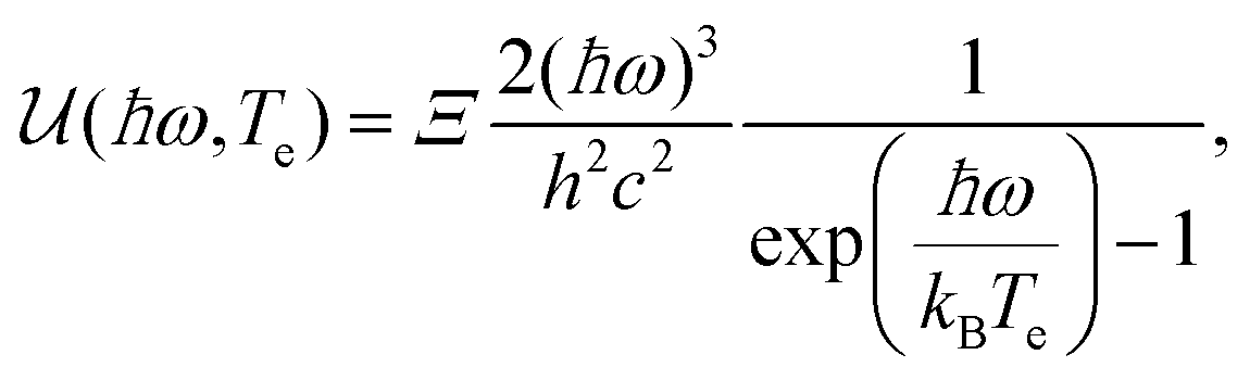 | (31) |
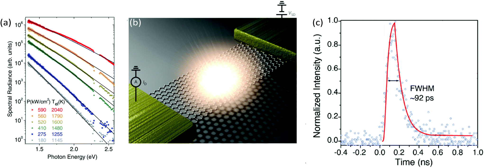 | ||
| Fig. 22 (a) Spectral radiance of graphene under electrical bias measured as a function of the electrical power density P dissipated in the channel (dots). The measurements are fitted to Planck's law (eqn (31), solid lines) with the indicated Te. (b) Schematic of a suspended graphene. Under electrical bias, light is emitted mainly from the center of the graphene sheet. (c) Generation of short (∼92 ps) light pulses from a graphene light emitter excited by a 80 ps electrical pulse, which translates into to a bandwidth of 10 GHz. Panel (a) is reproduced with permission from ref. 78 (Copyright 2010 American Physical Society). Panel (b) is reproduced with permission from ref. 26 (Copyright2015 Springer Nature). Panel (c) is reproduced with permission from ref. 320 (Copyright 2018 American Chemical Society). | ||
Several approaches have been investigated to improve the emission efficiency of graphene emitters. To reduce vertical heat dissipation, Kim et al.26 fabricated suspended graphene emitters (see Fig. 22b) and demonstrated high thermal emission in the visible range. In these devices, hot carriers with temperatures up to nearly 3000 K are localized at the center the graphene layer electronic, resulting in more efficient (∼4 × 10⁻³) and brighter emission. However, suspended devices must operate in vacuum since graphene quickly oxidizes at high temperature. hBN encapsulation was found to provide excellent protection for graphene even at temperatures above 2000 K.320–324 These emitters have a measured efficiency of ∼1.6 × 10⁻⁵ and an estimated lifetime exceeding 4 years.320,321 These results were attributed in part to the efficient cooling of the hot carriers into the hBN mediated by coupling to hybrid polaritonic modes (see section 3.2.3). Finally, another avenue to enhance Joule heating and thermal radiation in graphene is to confine the current flow through a narrow constriction.324
Furthermore, the broad spectral emission of graphene emitters can be easily tailored to meet the needs of specific applications. This can be achieved by integrating the graphene emitter in a sub-wavelength optical structure which modifies the electromagnetic local density of state. Different structures have been demonstrated, including photonic microcavities26,320,321,324,325 and photonic crystals.323 The latter enabled the strongest modulation of the black-body radiation spectrum in the near-infrared region, which is relevant for optical communications.
Another important advantage of graphene emitters is their high-speed modulation rate, which is facilitated by the ultrafast dynamics of hot carriers. Indeed, recent studies28,320,323 reported a temporal response of ∼100 ps (see Fig. 22c) for various device architectures, corresponding to a modulation bandwidth of ∼10 GHz. This exceptional speed, several orders of magnitude faster than conventional thermal emitters, was attributed to the rapid cooling of hot carriers, mainly due to remote heat to the hBN or SiO2 substrates. Real-time optical communications at 50 Mbps was demonstrated by coupling directly the emitter with an optical fiber.28 These results demonstrate the potential of graphene emitters as chip-integrated light sources for telecom and datacom applications.
7 Discussion and outlook
In this section we first discuss what sets apart the properties of hot carriers in graphene, compared to the properties of hot carriers in common metals. We then provide a brief comparison with hot-carrier phenomena in other material systems with Dirac electrons. Finally, we will mention some emerging potential applications of hot Dirac carriers.7.1 Graphene vs. common metals
As we have shown throughout this review, hot carriers play an important role in the electrical and optical response of graphene. We note that semiconducting two-dimensional material systems can also exhibit important physical effects related to hot carriers. Nevertheless, the vanishing band gap, linear energy–momentum dispersion relation, and strong carrier–carrier interactions of the Dirac fermions in graphene set graphene apart. One important consequence of these properties is graphene's small electronic heat capacity Ce and heat transfer coefficient Γcool, which mainly stem from graphene's low charge carrier density. To emphasize this point, it is instructive to examine and compare the behaviour of hot carriers in other systems. Hot carriers have been studied in metals, in particular gold, for over 50 years.11,326–335 At room temperature, the electron–phonon coupling in gold leads to a Γcool of ∼2.2 × 10¹⁶ W m−3 K−1.336 Even when considering an hypothetical layer of gold as thin as graphene, Γcool,2D ∼ 7 MW m−2 K−1 is two orders of magnitude larger than that of graphene in most conditions. For instance, for hBN-encapsulated graphene at room temperature, the estimated Γcool mediated by hyperbolic phonons is <0.1 MW m−2 K−1 for |μ| < 0.2 eV.92 Hence, under steady state conditions (see eqn (3)) and for a given input power, the excess electronic temperature ΔTe in gold is ∼100 times smaller than in graphene. For that reason, hot carrier effects in gold are typically observed in transport measurements only at low temperature (<100 mK), where the electron–phonon coupling is drastically reduced.328,332 Alternatively, hot carriers can also be generated by short intense laser pulse. In this case, Te is determined by the heat capacity coefficient γ (see eqn (6)), which in the case of gold is 68 J m−3 K−2. Here again, the equivalent 2D value (γ2D ∼ 2 × 10⁻⁸ J m−2 K−2) is roughly two orders of magnitude larger than that of graphene (<8 × 10⁻¹⁰ J m−2 K−2 for |μ| < 0.2 eV, see eqn (4)), a difference which is mainly due to the large charge carrier density (or Fermi energy) in gold, compared to graphene. This implies that for the same input fluence, the initial in graphene can be significantly larger than in gold. Interestingly, these hot carriers will cool down with a similar timescale τcool = Ce/Γcool ∼ 1–2 ps.331 We also note that the carrier heating time in metals (τheat ∼ 350–500 fs)331,334 is significantly longer than in graphene (<100 fs),37,45 which leads to higher heating efficiency in the latter. All these differences help explain the preponderance of hot carrier effects in graphene as compared to conventional metals.
7.2 Other Dirac-electron systems
Besides graphene, there are several other material systems with Dirac electrons, characterized by a linear energy–momentum dispersion relation. It can be expected that similar hot-carrier effects as in graphene play a role in these materials. We will discuss several quantum materials, starting with topological insulators. These are material systems that are semiconducting in the bulk, whereas on the surface (for 3D systems) or edge (for 2D systems), protected conducting states emerge with nearly linear dispersion (see the review of ref. 337). OPTP experiments on Bi2Se3338 showed the occurrence of negative photoconductivity (a decrease in THz conductivity after photoexcitation). This is similar to OPTP experiments on graphene, where negative photoconductivity was interpreted as a signature of hot carriers.34 Time-resolved ARPES measurements with visible pump light performed on Bi2Se3339,340 and Bi2Te3341 discussed the photo-induced carrier thermalization and cooling dynamics. In contrast with graphene, in these topological-insulator systems, the presence of bulk bands leads to complex dynamics involving an interplay between bulk and surface charges. There have been several attempts to eliminate the effects of bulk charges, for example by studying topological insulators excited by THz and mid-infrared light, such that no interband absorption takes place. For example, Luo et al. recently used this approach to demonstrate faster dynamics for hot surface-state carriers compared to hot bulk carriers, for Bi2Se3 at 5 K.324 At room temperature, the experimentally observed dynamics became similar, which is due to efficient surface–bulk coupling, as explained in ref. 339. As a result of the surface–bulk interactions, the precise dynamics of hot Dirac carriers in topological insulators are currently still under debate.
Another quantum material system that hosts Dirac electrons is the 3D Dirac semimetal Cd3As2.342 Optical pump–probe measurements showed clear signatures that are consistent with the formation of a hot-carrier distribution on a timescale of ∼400 fs.343 Cooling was observed to be slower than in graphene. An OPTP study showed fluence- and temperature-dependent cooling dynamics with two time constants – one on the order of a few ps, and one that is up to ∼8 ps.344 These dynamics were interpreted within a cooling model that has also been used for graphene: initial fast decay by optical phonon emission, followed by “anharmonic” phonon decay. Interestingly, in ref. 344 a positive THz photoconductivity was observed, which was also observed by Zhang et al.160 and Cheng et al.163 In graphene, a positive photoconductivity was only found close to the Dirac point, for EF below ∼100 meV,57,137,139 as a result of interband thermalization.35 The origin of the positive photoconductivity observed for Cd3As2 is still under debate.
Given these similarities in heating–cooling dynamics of different Dirac electron systems, we could expect that similar technological applications as those discussed in section 6 are possible. Topological insulator materials such as Bi2Te3 have been known for their large Seebeck coefficients (see for example this review by Xu et al.345). Not surprisingly, it has been shown that significant photo-thermoelectric currents can be generated,346,347 similar to graphene. Furthermore, using the 3D semimetal Cd3As2, ultrafast, broadband photodetection based on the photo-thermoelectric effect has been demonstrated.348 Also in the field of nonlinear light conversion, different Dirac materials have generated interesting results. Terahertz nonlinearities, for example, have been shown to originate from Dirac surface states in Bi2Se3,349 and, very recently, THz harmonics have been generated from Cd3As2.163,350 We should note that in the latter case, the role of the hot carriers is debated, as these results were described using coherent carrier acceleration, rather than the thermodynamic nonlinearity that is responsible for the exceptionally large THz nonlinearity in the case of graphene (see Fig. 14).
8 Conclusion
In this review, we have described fundamental properties of hot carriers in graphene, and systems that exploit hot carriers towards useful applications with a large potential to have an important impact on society. Whereas on a fundamental level many physical phenomena are well understood, we conclude that several areas are still subjected to debate, and therefore anticipate the continuous development of novel insights. As an example, we refer to the many competing cooling mechanisms that have been identified in recent years (see section 3). Besides continuing the pursuit of a detailed understanding of the fundamental physics of hot carriers in graphene itself, a highly promising research direction is that of graphene interfaced with other (2D) materials. We have discussed a few examples of such systems, where the substrate of graphene, or adjacent 2D materials, play an important role in determining the overall system properties, in particular related to transport (see section 5). Another highly interesting avenue is that of graphene interfaced with graphene itself. For example, we note that exciting hot-carrier dynamics have been observed for 30°-twisted bilayer graphene,351 and have been predicted for graphene Moiré superlattices.352. Finally, we note that besides the optical and optoelectronic applications that we have focused on in section 6, there are several predictions and preliminary results related to applications, for example hot-carrier transistors353,354 and hot-carrier enabled energy-harvesting devices.257,355 Thus, we expect hot Dirac carriers to continue to give rise to interesting physics and promising applications.Conflicts of interest
There are no conflicts to declare.Acknowledgements
ICN2 was supported by the Severo Ochoa program from Spanish MINECO (grant no. SEV-2017-0706). K. J. T. acknowledges funding from the European Union's Horizon 2020 research and innovation program under grant agreement no. 804349 (ERC StG CUHL), RyC fellowship no. RYC-2017-22330, IAE project PID2019-111673GB-I00, and financial support through the MAINZ Visiting Professorship. G. S. acknowledges funding from the European Union's Horizon 2020 research and innovation program under grant agreement GrapheneCore3 881603, the German Research Foundation DFG (CRC 1375 NOA, project B5) and the Daimler und Benz foundation. M. M. acknowledges support from the Natural Sciences and Engineering Research Council of Canada (PDF-516936-2018) and from the Canada First Research Excellence Fund. A. P. is supported by the European Commission under the EU Horizon 2020 MSCA-RISE-2019 programme (project 873028 HYDROTRONICS). A. P. also acknowledges support of the Leverhulme Trust under the grant RPG-2019-363.References
- P. A. George, J. Strait, J. Dawlaty, S. Shivaraman, M. Chandrashekhar, F. Rana and M. G. Spencer, Nano Lett., 2008, 8, 4248–4251 CrossRef CAS PubMed.
- D. Sun, Z.-K. Wu, C. Divin, X. Li, C. Berger, W. A. de Heer, P. N. First and T. B. Norris, Phys. Rev. Lett., 2008, 101, 157402 CrossRef PubMed.
- J. M. Dawlaty, S. Shivaraman, M. Chandrashekhar, F. Rana and M. G. Spencer, Appl. Phys. Lett., 2008, 92, 042116 CrossRef.
- I. Meric, M. Y. Han, A. F. Young, B. Ozyilmaz, P. Kim and K. L. Shepard, Nat. Nanotechnol., 2008, 3, 654–659 CrossRef CAS PubMed.
- S. Butscher, F. Milde, M. Hirtschulz, E. Malić and A. Knorr, Appl. Phys. Lett., 2007, 91, 203103 CrossRef.
- E. H. Hwang, B. Y. K. Hu and S. Das Sarma, Phys. Rev. B: Condens. Matter Mater. Phys., 2007, 76, 1–6 Search PubMed.
- T. Hertel and G. Moos, Phys. Rev. Lett., 2000, 84, 5002–5005 CrossRef CAS PubMed.
- O. J. Korovyanko, C. X. Sheng, Z. V. Vardeny, A. B. Dalton and R. H. Baughman, Phys. Rev. Lett., 2004, 92, 4 CrossRef PubMed.
- J. C. Charlier, P. C. Eklund, J. Zhu and A. C. Ferrari, Top. Appl. Phys., 2008, 111, 673–709 CrossRef.
- P. Avouris, M. Freitag and V. Perebeinos, Nat. Photonics, 2008, 2, 341–350 CrossRef CAS.
- M. L. Brongersma, N. J. Halas and P. Nordlander, Nat. Nanotechnol., 2015, 10, 25–34 CrossRef CAS PubMed.
- F. H. L. Koppens, T. Mueller, P. Avouris, A. C. Ferrari, M. S. Vitiello and M. Polini, Nat. Nanotechnol., 2014, 9, 780–793 CrossRef CAS PubMed.
- M. Romagnoli, V. Sorianello, M. Midrio, F. H. L. Koppens, C. Huyghebaert, D. Neumaier, P. Galli, W. Templ, A. D'Errico and A. C. Ferrari, Nat. Rev. Mater., 2018, 3, 392–414 CrossRef CAS.
- J. You, S. Bongu, Q. Bao and N. Panoiu, Nanophotonics, 2018, 8, 63–97 Search PubMed.
- A. Autere, H. Jussila, Y. Dai, Y. Wang, H. Lipsanen and Z. Sun, Adv. Mater., 2018, 30, 1705963 CrossRef PubMed.
- J. C. W. Song and L. S. Levitov, J. Phys.: Condens. Matter, 2015, 27, 164201 CrossRef PubMed.
- Z.-Y. Ong and M.-H. Bae, 2D Mater., 2019, 6, 032005 CrossRef CAS.
- Y. M. Zuev, W. Chang and P. Kim, Phys. Rev. Lett., 2009, 102, 096807 CrossRef PubMed.
- P. Wei, W. Bao, Y. Pu, C. N. Lau and J. Shi, Phys. Rev. Lett., 2009, 102, 166808 CrossRef PubMed.
- K. L. Grosse, M.-H. Bae, F. Lian, E. Pop and W. P. King, Nat. Nanotechnol., 2011, 6, 287–290 CrossRef CAS PubMed.
- A. C. Betz, S. H. Jhang, E. Pallecchi, R. Ferreira, G. Fève, J.-M. M. Berroir and B. Plaçais, Nat. Phys., 2013, 9, 109–112 Search PubMed.
- W. Yang, S. Berthou, X. Lu, Q. Wilmart, A. Denis, M. Rosticher, T. Taniguchi, K. Watanabe, G. Fève, J.-M. Berroir, G. Zhang, C. Voisin, E. Baudin and B. Plaçais, Nat. Nanotechnol., 2018, 13, 47–52 CrossRef CAS PubMed.
- M. Freitag, M. Steiner, Y. Martin, V. Perebeinos, Z. Chen, J. C. Tsang and P. Avouris, Nano Lett., 2009, 9, 1883–1888 CrossRef CAS PubMed.
- D.-H. Chae, B. Krauss, K. von Klitzing and J. H. Smet, Nano Lett., 2010, 10, 466–471 CrossRef CAS PubMed.
- M. Freitag, H.-Y. Chiu, M. Steiner, V. Perebeinos and P. Avouris, Nat. Nanotechnol., 2010, 5, 497–501 CrossRef CAS PubMed.
- Y. D. Kim, H. Kim, Y. Cho, J. H. Ryoo, C.-H. Park, P. Kim, Y. S. Kim, S. Lee, Y. Li, S.-N. Park, Y. Shim Yoo, D. Yoon, V. E. Dorgan, E. Pop, T. F. Heinz, J. Hone, S.-H. Chun, H. Cheong, S. W. Lee, M.-H. Bae and Y. D. Park, Nat. Nanotechnol., 2015, 10, 676–681 CrossRef CAS PubMed.
- N. H. Mahlmeister, L. M. Lawton, I. J. Luxmoore and G. R. Nash, Appl. Phys. Express, 2016, 9, 012105 CrossRef.
- Y. Miyoshi, Y. Fukazawa, Y. Amasaka, R. Reckmann, T. Yokoi, K. Ishida, K. Kawahara, H. Ago and H. Maki, Nat. Commun., 2018, 9, 1279 CrossRef PubMed.
- J. K. Viljas and T. T. Heikkilä, Phys. Rev. B: Condens. Matter Mater. Phys., 2010, 81, 245404 CrossRef.
- C. H. Lui, K. F. Mak, J. Shan and T. F. Heinz, Phys. Rev. Lett., 2010, 105, 127404 CrossRef PubMed.
- K. C. Fong, E. E. Wollman, H. Ravi, W. Chen, A. A. Clerk, M. D. Shaw, H. G. Leduc and K. C. Schwab, Phys. Rev. X, 2013, 3, 041008 CAS.
- R. Kokkoniemi, J.-P. Girard, D. Hazra, A. Laitinen, J. Govenius, R. E. Lake, I. Sallinen, V. Vesterinen, M. Partanen, J. Y. Tan, K. W. Chan, K. Y. Tan, P. Hakonen and M. Möttönen, Nature, 2020, 586, 47–51 CrossRef CAS PubMed.
- M. W. Graham, S.-F. F. Shi, D. C. Ralph, J. Park and P. L. McEuen, Nat. Phys., 2013, 9, 103–108 Search PubMed.
- K. J. Tielrooij, J. C. W. Song, S. A. Jensen, A. Centeno, A. Pesquera, A. Zurutuza Elorza, M. Bonn, L. S. Levitov and F. H. L. Koppens, Nat. Phys., 2013, 9, 248–252 Search PubMed.
- A. Tomadin, S. M. Hornett, H. I. Wang, E. M. Alexeev, A. Candini, C. Coletti, D. Turchinovich, M. Kläui, M. Bonn, F. H. L. Koppens, E. Hendry, M. Polini and K.-J. Tielrooij, Sci. Adv., 2018, 4, eaar5313 Search PubMed.
- A. H. Castro Neto, F. Guinea, N. M. R. Peres, K. S. Novoselov and A. K. Geim, Rev. Mod. Phys., 2009, 81, 109–162 CrossRef CAS.
- I. Gierz, J. C. Petersen, M. Mitrano, C. Cacho, I. C. E. Turcu, E. Springate, A. Stöhr, A. Köhler, U. Starke and A. Cavalleri, Nat. Mater., 2013, 12, 1119–1124 CrossRef CAS PubMed.
- J. C. Johannsen, S. Ulstrup, F. Cilento, A. Crepaldi, M. Zacchigna, C. Cacho, I. C. E. Turcu, E. Springate, F. Fromm, C. Raidel, T. Seyller, F. Parmigiani, M. Grioni and P. Hofmann, Phys. Rev. Lett., 2013, 111, 027403 CrossRef PubMed.
- G. Rohde, A. Stange, A. Müller, M. Behrendt, L.-P. Oloff, K. Hanff, T. J. Albert, P. Hein, K. Rossnagel and M. Bauer, Phys. Rev. Lett., 2018, 121, 256401 CrossRef CAS PubMed.
- T. Fang, A. Konar, H. Xing and D. Jena, Appl. Phys. Lett., 2007, 91, 092109 CrossRef.
- V. E. Dorgan, A. Behnam, H. J. Conley, K. I. Bolotin and E. Pop, Nano Lett., 2013, 13, 4581–4586 CrossRef PubMed.
- J. C. W. Song, K. J. Tielrooij, F. H. L. Koppens and L. S. Levitov, Phys. Rev. B: Condens. Matter Mater. Phys., 2013, 87, 155429 CrossRef.
- J. C. Johannsen, S. Ulstrup, A. Crepaldi, F. Cilento, M. Zacchigna, J. A. Miwa, C. Cacho, R. T. Chapman, E. Springate, F. Fromm, C. Raidel, T. Seyller, P. D. C. King, F. Parmigiani, M. Grioni and P. Hofmann, Nano Lett., 2015, 15, 326–331 CrossRef CAS PubMed.
- S. Wu, L. Wang, Y. Lai, W.-Y. Shan, G. Aivazian, X. Zhang, T. Taniguchi, K. Watanabe, D. Xiao, C. Dean, J. Hone, Z. Li and X. Xu, Sci. Adv., 2016, 2 CAS , e1600002.
- D. Brida, A. Tomadin, C. Manzoni, Y. J. Kim, A. Lombardo, S. Milana, R. R. Nair, K. S. Novoselov, A. C. Ferrari, G. Cerullo and M. Polini, Nat. Commun., 2013, 4, 1987 CrossRef CAS PubMed.
- F. Kadi, T. Winzer, A. Knorr and E. Malic, Sci. Rep., 2015, 5, 16841 CrossRef CAS PubMed.
- J. C. König-Otto, M. Mittendorff, T. Winzer, F. Kadi, E. Malic, A. Knorr, C. Berger, W. A. de Heer, A. Pashkin, H. Schneider, M. Helm and S. Winnerl, Phys. Rev. Lett., 2016, 117, 087401 CrossRef PubMed.
- E. H. Hwang and S. Das Sarma, Phys. Rev. B: Condens. Matter Mater. Phys., 2007, 75, 205418 CrossRef.
- A. Tomadin, D. Brida, G. Cerullo, A. C. Ferrari and M. Polini, Phys. Rev. B: Condens. Matter Mater. Phys., 2013, 88, 035430 CrossRef.
- T. Winzer, A. Knorr and E. Malic, Nano Lett., 2010, 10, 4839–4843 CrossRef CAS PubMed.
- T. Plötzing, T. Winzer, E. Malic, D. Neumaier, A. Knorr and H. Kurz, Nano Lett., 2014, 14, 5371–5375 CrossRef PubMed.
- W. Shockley and H. J. Queisser, J. Appl. Phys., 1961, 32, 510–519 CrossRef CAS.
- K. J. Tielrooij, L. Piatkowski, M. Massicotte, A. Woessner, Q. Ma, Y. Lee, K. S. Myhro, C. N. Lau, P. Jarillo-Herrero, N. F. van Hulst and F. H. L. Koppens, Nat. Nanotechnol., 2015, 10, 437–443 CrossRef CAS PubMed.
- Z. Mics, K.-J. Tielrooij, K. Parvez, S. a. Jensen, I. Ivanov, X. Feng, K. Müllen, M. Bonn and D. Turchinovich, Nat. Commun., 2015, 6, 7655 CrossRef CAS PubMed.
- S. Castilla, B. Terrés, M. Autore, L. Viti, J. Li, A. Y. Nikitin, I. Vangelidis, K. Watanabe, T. Taniguchi, E. Lidorikis, M. S. Vitiello, R. Hillenbrand, K.-J. Tielrooij and F. H. Koppens, Nano Lett., 2019, 19, 2765–2773 CrossRef CAS PubMed.
- H. A. Hafez, S. Kovalev, J.-C. Deinert, Z. Mics, B. Green, N. Awari, M. Chen, S. Germanskiy, U. Lehnert, J. Teichert, Z. Wang, K.-J. Tielrooij, Z. Liu, Z. Chen, A. Narita, K. Müllen, M. Bonn, M. Gensch and D. Turchinovich, Nature, 2018, 561, 507–511 CrossRef CAS PubMed.
- S. A. Jensen, Z. Mics, I. Ivanov, H. S. Varol, D. Turchinovich, F. H. L. Koppens, M. Bonn and K. J. Tielrooij, Nano Lett., 2014, 14, 5839–5845 CrossRef CAS PubMed.
- M. Mittendorff, T. Winzer, E. Malic, A. Knorr, C. Berger, W. A. de Heer, H. Schneider, M. Helm and S. Winnerl, Nano Lett., 2014, 14, 1504–1507 CrossRef CAS PubMed.
- L. Fritz, J. Schmalian, M. Müller and S. Sachdev, Phys. Rev. B: Condens. Matter Mater. Phys., 2008, 78, 085416 CrossRef.
- Q. Ma, C. H. Lui, J. C. W. Song, Y. Lin, J. F. Kong, Y. Cao, T. H. Dinh, N. L. Nair, W. Fang, K. Watanabe, T. Taniguchi, S.-Y. Xu, J. Kong, T. Palacios, N. Gedik, N. M. Gabor and P. Jarillo-Herrero, Nat. Nanotechnol., 2019, 14, 145–150 CrossRef CAS PubMed.
- P. Gallagher, C.-s. Yang, T. Lyu, F. Tian, R. Kou, H. Zhang, K. Watanabe, T. Taniguchi and F. Wang, Science, 2019, 162, eaat8687 CrossRef PubMed.
- M. Kim, S. G. Xu, A. I. Berdyugin, A. Principi, S. Slizovskiy, N. Xin, P. Kumaravadivel, W. Kuang, M. Hamer, R. Krishna Kumar, R. V. Gorbachev, K. Watanabe, T. Taniguchi, I. V. Grigorieva, V. I. Fal'ko, M. Polini and A. K. Geim, Nat. Commun., 2020, 11, 2339 CrossRef CAS PubMed.
- P. Plochocka, P. Kossacki, A. Golnik, T. Kazimierczuk, C. Berger, W. A. De Heer and M. Potemski, Phys. Rev. B: Condens. Matter Mater. Phys., 2009, 80, 1–5 CrossRef.
- L. D. Landau, E. M. Lifshitz and L. P. Pitaevskij, Course of theoretical physics. vol. 10: Physical kinetics, 1981 Search PubMed.
- C. Di Castro and R. Raimondi, Statistical Mechanics and Applications in Condensed Matter, 2015 Search PubMed.
- N. W. Ashcroft and N. D. Mermin, Solid State Physics, Cornell University, 1976 Search PubMed.
- D. Xiao, M.-C. Chang and Q. Niu, Rev. Mod. Phys., 2010, 82, 1959–2007 CrossRef CAS.
- S. Chapman, T. G. Cowling and D. Burnett, The mathematical theory of non-uniform gases: an account of the kinetic theory of viscosity, thermal conduction and diffusion in gases, 1990 Search PubMed.
- N. Mounet and N. Marzari, Phys. Rev. B: Condens. Matter Mater. Phys., 2005, 71, 205214 CrossRef.
- S. Piscanec, M. Lazzeri, F. Mauri, A. C. Ferrari and J. Robertson, Phys. Rev. Lett., 2004, 93, 185503 CrossRef CAS PubMed.
- S. Piscanec, M. Lazzeri, J. Robertson, A. C. Ferrari and F. Mauri, Phys. Rev. B: Condens. Matter Mater. Phys., 2007, 75, 035427 CrossRef.
- T. Sohier, M. Calandra, C.-H. Park, N. Bonini, N. Marzari and F. Mauri, Phys. Rev. B: Condens. Matter Mater. Phys., 2014, 90, 125414 CrossRef.
- F. Rana, P. A. George, J. H. Strait, J. Dawlaty, S. Shivaraman, M. Chandrashekhar and M. G. Spencer, Phys. Rev. B: Condens. Matter Mater. Phys., 2009, 79, 115447 CrossRef.
- H. Wang, J. H. Strait, P. A. George, S. Shivaraman, V. B. Shields, M. Chandrashekhar, J. Hwang, F. Rana, M. G. Spencer, C. S. Ruiz-Vargas and J. Park, Appl. Phys. Lett., 2010, 96, 081917 CrossRef.
- T. Kampfrath, L. Perfetti, F. Schapper, C. Frischkorn and M. Wolf, Phys. Rev. Lett., 2005, 95, 187403 CrossRef PubMed.
- M. Breusing, S. Kuehn, T. Winzer, E. Malić, F. Milde, N. Severin, J. P. Rabe, C. Ropers, A. Knorr and T. Elsaesser, Phys. Rev. B: Condens. Matter Mater. Phys., 2011, 83, 153410 CrossRef.
- L. M. Malard, K. Fai Mak, A. H. Castro Neto, N. M. R. Peres and T. F. Heinz, New J. Phys., 2013, 15, 015009 CrossRef CAS.
- S. Berciaud, M. Y. Han, K. F. Mak, L. E. Brus, P. Kim and T. F. Heinz, Phys. Rev. Lett., 2010, 104, 227401 CrossRef PubMed.
- K. Kang, D. Abdula, D. G. Cahill and M. Shim, Phys. Rev. B: Condens. Matter Mater. Phys., 2010, 81, 165405 CrossRef.
- S. Wu, W.-T. Liu, X. Liang, P. J. Schuck, F. Wang, Y. R. Shen and M. Salmeron, Nano Lett., 2012, 12, 5495–5499 CrossRef CAS PubMed.
- N. Bonini, M. Lazzeri, N. Marzari and F. Mauri, Phys. Rev. Lett., 2007, 99, 176802 CrossRef PubMed.
- N. M. Gabor, J. C. W. Song, Q. Ma, N. L. Nair, T. Taychatanapat, K. Watanabe, T. Taniguchi, L. S. Levitov and P. Jarillo-Herrero, Science, 2011, 334, 648–652 CrossRef CAS PubMed.
- M. T. Mihnev, F. Kadi, C. J. Divin, T. Winzer, S. Lee, C.-h. Liu, Z. Zhong, C. Berger, W. A. de Heer, E. Malic, A. Knorr and T. B. Norris, Nat. Commun., 2016, 7, 11617 CrossRef CAS PubMed.
- E. A. A. Pogna, X. Jia, A. Principi, A. Block, L. Banszerus, J. Zhang, X. Liu, T. Sohier, S. Forti, K. Soundarapandian, B. Terrés, J. D. Mehew, C. Trovatello, C. Coletti, F. H. L. Koppens, M. Bonn, N. van Hulst, M. J. Verstraete, H. Peng, Z. Liu, C. Stampfer, G. Cerullo and K.-J. Tielrooij, 2021, arXiv:2103.03527.
- J. C. W. Song, M. Y. Reizer and L. S. Levitov, Phys. Rev. Lett., 2012, 109, 106602 CrossRef PubMed.
- K. Kaasbjerg, K. S. Thygesen and K. W. Jacobsen, Phys. Rev. B: Condens. Matter Mater. Phys., 2012, 85, 165440 CrossRef.
- R. Bistritzer and A. H. MacDonald, Phys. Rev. Lett., 2009, 102, 206410 CrossRef CAS PubMed.
- A. C. Betz, F. Vialla, D. Brunel, C. Voisin, M. Picher, A. Cavanna, A. Madouri, G. Fève, J.-M. Berroir, B. Plaçais and E. Pallecchi, Phys. Rev. Lett., 2012, 109, 056805 CrossRef CAS PubMed.
- M. W. Graham, S.-F. Shi, Z. Wang, D. C. Ralph, J. Park and P. L. McEuen, Nano Lett., 2013, 13, 5497–5502 CrossRef CAS PubMed.
- T. V. Alencar, M. G. Silva, L. M. Malard and A. M. de Paula, Nano Lett., 2014, 14, 5621–5624 CrossRef CAS PubMed.
- A. Principi, M. B. Lundeberg, N. C. H. Hesp, K.-J. Tielrooij, F. H. L. Koppens and M. Polini, Phys. Rev. Lett., 2017, 118, 126804 CrossRef PubMed.
- K.-J. J. Tielrooij, N. C. H. Hesp, A. Principi, M. B. Lundeberg, E. A. A. Pogna, L. Banszerus, Z. Mics, M. Massicotte, P. Schmidt, D. Davydovskaya, D. G. Purdie, I. Goykhman, G. Soavi, A. Lombardo, K. Watanabe, T. Taniguchi, M. Bonn, D. Turchinovich, C. Stampfer, A. C. Ferrari, G. Cerullo, M. Polini and F. H. L. Koppens, Nat. Nanotechnol., 2018, 13, 41–46 CrossRef CAS PubMed.
- T. Low, V. Perebeinos, R. Kim, M. Freitag and P. Avouris, Phys. Rev. B: Condens. Matter Mater. Phys., 2012, 86, 045413 CrossRef.
- Z. Jacob, J. Y. Kim, G. V. Naik, A. Boltasseva, E. E. Narimanov and V. M. Shalaev, Appl. Phys. B: Lasers Opt., 2010, 100, 215–218 CrossRef CAS.
- M. N. Gjerding, R. Petersen, T. G. Pedersen, N. A. Mortensen and K. S. Thygesen, Nat. Commun., 2017, 8, 320 CrossRef CAS PubMed.
- C. R. Dean, a. F. Young, I. Meric, C. Lee, L. Wang, S. Sorgenfrei, K. Watanabe, T. Taniguchi, P. Kim, K. L. Shepard and J. Hone, Nat. Nanotechnol., 2010, 5, 722–726 CrossRef CAS PubMed.
- L. Wang, I. Meric, P. Y. Huang, Q. Gao, Y. Gao, H. Tran, T. Taniguchi, K. Watanabe, L. M. Campos, D. a. Muller, J. Guo, P. Kim, J. Hone, K. L. Shepard and C. R. Dean, Science, 2013, 342, 614–617 CrossRef CAS PubMed.
- J. D. Caldwell, A. V. Kretinin, Y. Chen, V. Giannini, M. M. Fogler, Y. Francescato, C. T. Ellis, J. G. Tischler, C. R. Woods, A. J. Giles, M. Hong, K. Watanabe, T. Taniguchi, S. A. Maier and K. S. Novoselov, Nat. Commun., 2014, 5, 1–9 Search PubMed.
- J. Crossno, J. K. Shi, K. Wang, X. Liu, A. Harzheim, A. Lucas, S. Sachdev, P. Kim, T. Taniguchi, K. Watanabe, T. A. Ohki and K. C. Fong, Science, 2016, 351, 1058–1061 CrossRef CAS PubMed.
- J. M. Hamm, A. F. Page, J. Bravo-Abad, F. J. Garcia-Vidal and O. Hess, Phys. Rev. B, 2016, 93, 041408 CrossRef.
- L. Kim, S. Kim, P. K. Jha, V. W. Brar and H. A. Atwater, 2020, arXiv:2001.11052.
- R. Yu, A. Manjavacas and F. J. García de Abajo, Nat. Commun., 2017, 8, 2 CrossRef PubMed.
- D. Halbertal, M. Ben Shalom, A. Uri, K. Bagani, A. Y. Meltzer, I. Marcus, Y. Myasoedov, J. Birkbeck, L. S. Levitov, A. K. Geim and E. Zeldov, Science, 2017, 358, 1303–1306 CrossRef CAS PubMed.
- K. C. Fong and K. C. Schwab, Phys. Rev. X, 2012, 2, 031006 Search PubMed.
- M. R. Arai, Appl. Phys. Lett., 1983, 42, 906–908 CrossRef.
- M. M. Jadidi, R. J. Suess, C. Tan, X. Cai, K. Watanabe, T. Taniguchi, A. B. Sushkov, M. Mittendorff, J. Hone, H. D. Drew, M. S. Fuhrer and T. E. Murphy, Phys. Rev. Lett., 2016, 117, 257401 CrossRef PubMed.
- A. M. Weiner, Ultrafast Time-Resolved Spectroscopy, John Wiley & Sons Ltd, 2009, ch. 9, pp. 422–506 Search PubMed.
- R. Ulbricht, E. Hendry, J. Shan, T. F. Heinz and M. Bonn, Rev. Mod. Phys., 2011, 83, 543–586 CrossRef CAS.
- G. Soavi, F. Scotognella, G. Lanzani and G. Cerullo, Adv. Opt. Mater., 2016, 4, 1670–1688 CrossRef CAS.
- A. Grupp, A. Budweg, M. P. Fischer, J. Allerbeck, G. Soavi, A. Leitenstorfer and D. Brida, J. Opt., 2018, 20, 014005 CrossRef.
- C. L. Smallwood, R. A. Kaindl and A. Lanzara, EPL, 2016, 115, 27001 CrossRef.
- A. Urich, K. Unterrainer and T. Mueller, Nano Lett., 2011, 11, 2804–2808 CrossRef CAS PubMed.
- D. Sun, G. Aivazian, A. M. Jones, J. S. Ross, W. Yao, D. Cobden and X. Xu, Nat. Nanotechnol., 2012, 7, 114–118 CrossRef CAS PubMed.
- K. J. Tielrooij, M. Massicotte, L. Piatkowski, A. Woessner, Q. Ma, P. Jarillo-Herrero, N. F. V. Hulst and F. H. L. Koppens, J. Phys.: Condens. Matter, 2015, 27, 164207 CrossRef CAS PubMed.
- N. M. R. Peres, Rev. Mod. Phys., 2010, 82, 2673–2700 CrossRef CAS.
- T. Ando, Y. Zheng and H. Suzuura, J. Phys. Soc. Jpn., 2002, 71, 1318–1324 CrossRef CAS.
- S. Ryu, C. Mudry, A. Furusaki and A. W. W. Ludwig, Phys. Rev. B: Condens. Matter Mater. Phys., 2007, 75, 205344 CrossRef.
- V. P. Gusynin and S. G. Sharapov, Phys. Rev. B: Condens. Matter Mater. Phys., 2006, 73, 245411 CrossRef.
- L. A. Falkovsky and A. A. Varlamov, Eur. Phys. J. B, 2007, 56, 281–284 CrossRef CAS.
- S. A. Mikhailov and K. Ziegler, Phys. Rev. Lett., 2007, 99, 016803 CrossRef CAS PubMed.
- L. Yang, J. Deslippe, C.-H. Park, M. L. Cohen and S. G. Louie, Phys. Rev. Lett., 2009, 103, 186802 CrossRef PubMed.
- S. Mikhailov, Microelectron. J., 2009, 40, 712–715 CrossRef CAS.
- S. Das Sarma, S. Adam, E. H. Hwang and E. Rossi, Rev. Mod. Phys., 2011, 83, 407–470 CrossRef CAS.
- R. R. Nair, P. Blake, A. N. Grigorenko, K. S. Novoselov, T. J. Booth, T. Stauber, N. M. R. Peres and A. K. Geim, Science, 2008, 320, 1308–1308 CrossRef CAS PubMed.
- K. F. Mak, M. Y. Sfeir, Y. Wu, C. H. Lui, J. A. Misewich and T. F. Heinz, Phys. Rev. Lett., 2008, 101, 196405 CrossRef PubMed.
- H. Choi, F. Borondics, D. A. Siegel, S. Y. Zhou, M. C. Martin, A. Lanzara and R. A. Kaindl, Appl. Phys. Lett., 2009, 94, 172102 CrossRef.
- K. F. Mak, J. Shan and T. F. Heinz, Phys. Rev. Lett., 2011, 106, 046401 CrossRef PubMed.
- J. Horng, C.-F. Chen, B. Geng, C. Girit, Y. Zhang, Z. Hao, H. A. Bechtel, M. Martin, A. Zettl, M. F. Crommie, Y. R. Shen and F. Wang, Phys. Rev. B: Condens. Matter Mater. Phys., 2011, 83, 165113 CrossRef.
- I. Ivanov, M. Bonn, Z. Mics and D. Turchinovich, EPL, 2015, 111, 67001 CrossRef.
- H. Yan, F. Xia, W. Zhu, M. Freitag, C. Dimitrakopoulos, A. A. Bol, G. Tulevski and P. Avouris, ACS Nano, 2011, 5, 9854–9860 CrossRef CAS PubMed.
- K. F. Mak, L. Ju, F. Wang and T. F. Heinz, Solid State Commun., 2012, 152, 1341–1349 CrossRef CAS.
- S. Winnerl, M. Orlita, P. Plochocka, P. Kossacki, M. Potemski, T. Winzer, E. Malic, A. Knorr, M. Sprinkle, C. Berger, W. A. de Heer, H. Schneider and M. Helm, Phys. Rev. Lett., 2011, 107, 237401 CrossRef CAS PubMed.
- A. B. Kuzmenko, E. van Heumen, F. Carbone and D. van der Marel, Phys. Rev. Lett., 2008, 100, 117401 CrossRef CAS PubMed.
- C.-F. Chen, C.-H. Park, B. W. Boudouris, J. Horng, B. Geng, C. Girit, A. Zettl, M. F. Crommie, R. A. Segalman, S. G. Louie and F. Wang, Nature, 2011, 471, 617–620 CrossRef CAS PubMed.
- M. Liu, X. Yin, E. Ulin-Avila, B. Geng, T. Zentgraf, L. Ju, F. Wang and X. Zhang, Nature, 2011, 474, 64–67 CrossRef CAS PubMed.
- A. J. Frenzel, C. H. Lui, W. Fang, N. L. Nair, P. K. Herring, P. Jarillo-Herrero, J. Kong and N. Gedik, Appl. Phys. Lett., 2013, 102, 113111 CrossRef.
- A. J. Frenzel, C. H. Lui, Y. C. Shin, J. Kong and N. Gedik, Phys. Rev. Lett., 2014, 113, 056602 CrossRef CAS PubMed.
- G. Jnawali, Y. Rao, H. Yan and T. F. Heinz, Nano Lett., 2013, 13, 524–530 CrossRef CAS PubMed.
- S.-F. Shi, T.-T. Tang, B. Zeng, L. Ju, Q. Zhou, A. Zettl and F. Wang, Nano Lett., 2014, 14, 1578–1582 CrossRef CAS PubMed.
- S. Savasta, O. Di Stefano and F. Nori, Nanophotonics, 2020, 10, 465–476 Search PubMed.
- H. Rostami and M. Polini, Phys. Rev. B, 2016, 93, 161411 CrossRef.
- J. L. Cheng, N. Vermeulen and J. E. Sipe, Sci. Rep., 2017, 7, 43843 CrossRef CAS PubMed.
- A. Marini, J. D. Cox and F. J. García de Abajo, Phys. Rev. B, 2017, 95, 125408 CrossRef.
- S. A. Mikhailov, Phys. Rev. B, 2019, 100, 115416 CrossRef CAS.
- N. Yoshikawa, T. Tamaya and K. Tanaka, Science, 2017, 356, 736–738 CrossRef CAS PubMed.
- N. Kumar, J. Kumar, C. Gerstenkorn, R. Wang, H.-Y. Chiu, A. L. Smirl and H. Zhao, Phys. Rev. B: Condens. Matter Mater. Phys., 2013, 87, 121406 CrossRef.
- S.-Y. Hong, J. I. Dadap, N. Petrone, P.-C. Yeh, J. Hone and R. M. Osgood, Phys. Rev. X, 2013, 3, 021014 Search PubMed.
- G. Soavi, G. Wang, H. Rostami, D. G. Purdie, D. De Fazio, T. Ma, B. Luo, J. Wang, A. K. Ott, D. Yoon, S. A. Bourelle, J. E. Muench, I. Goykhman, S. Dal Conte, M. Celebrano, A. Tomadin, M. Polini, G. Cerullo and A. C. Ferrari, Nat. Nanotechnol., 2018, 13, 583–588 CrossRef CAS PubMed.
- T. Jiang, D. Huang, J. Cheng, X. Fan, Z. Zhang, Y. Shan, Y. Yi, Y. Dai, L. Shi, K. Liu, C. Zeng, J. Zi, J. E. Sipe, Y.-R. Shen, W.-T. Liu and S. Wu, Nat. Photonics, 2018, 12, 430–436 CrossRef CAS.
- G. Soavi, G. Wang, H. Rostami, A. Tomadin, O. Balci, I. Paradisanos, E. A. A. Pogna, G. Cerullo, E. Lidorikis, M. Polini and A. C. Ferrari, ACS Photonics, 2019, 6, 2841–2849 CrossRef CAS.
- E. Hendry, P. J. Hale, J. Moger, A. K. Savchenko and S. A. Mikhailov, Phys. Rev. Lett., 2010, 105, 097401 CrossRef CAS PubMed.
- K. Alexander, N. A. Savostianova, S. A. Mikhailov, B. Kuyken and D. Van Thourhout, ACS Photonics, 2017, 4, 3039–3044 CrossRef CAS.
- N. An, T. Tan, Z. Peng, C. Qin, Z. Yuan, L. Bi, C. Liao, Y. Wang, Y. Rao, G. Soavi and B. Yao, Nano Lett., 2020, 20, 6473–6480 CrossRef CAS PubMed.
- Q. Bao, H. Zhang, Y. Wang, Z. Ni, Y. Yan, Z. X. Shen, K. P. Loh and D. Y. Tang, Adv. Funct. Mater., 2009, 19, 3077–3083 CrossRef CAS.
- A. Martinez and Z. Sun, Nat. Photonics, 2013, 7, 842–845 CrossRef CAS.
- E. Dremetsika, B. Dlubak, S.-P. Gorza, C. Ciret, M.-B. Martin, S. Hofmann, P. Seneor, D. Dolfi, S. Massar, P. Emplit and P. Kockaert, Opt. Lett., 2016, 41, 3281 CrossRef CAS PubMed.
- J. J. Dean and H. M. van Driel, Appl. Phys. Lett., 2009, 95, 261910 CrossRef.
- A. Y. Bykov, T. V. Murzina, M. G. Rybin and E. D. Obraztsova, Phys. Rev. B: Condens. Matter Mater. Phys., 2012, 85, 121413 CrossRef.
- Y. Q. An, F. Nelson, J. U. Lee and A. C. Diebold, Nano Lett., 2013, 13, 2104–2109 CrossRef CAS PubMed.
- Y. Zhang, D. Huang, Y. Shan, T. Jiang, Z. Zhang, K. Liu, L. Shi, J. Cheng, J. E. Sipe, W.-T. Liu and S. Wu, Phys. Rev. Lett., 2019, 122, 047401 CrossRef PubMed.
- S. A. Mikhailov, EPL, 2007, 79, 27002 CrossRef.
- S. A. Mikhailov and K. Ziegler, J. Phys.: Condens. Matter, 2008, 20, 384204 CrossRef CAS PubMed.
- B. Cheng, N. Kanda, T. N. Ikeda, T. Matsuda, P. Xia, T. Schumann, S. Stemmer, J. Itatani, N. P. Armitage and R. Matsunaga, Phys. Rev. Lett., 2020, 124, 117402 CrossRef CAS PubMed.
- S. A. Mikhailov, Phys. Rev. B, 2016, 93, 085403 CrossRef.
- J. L. Cheng, N. Vermeulen and J. E. Sipe, Phys. Rev. B: Condens. Matter Mater. Phys., 2015, 91, 235320 CrossRef.
- K. Alexander, N. A. Savostianova, S. A. Mikhailov, D. Van Thourhout and B. Kuyken, ACS Photonics, 2018, 5, 4944–4950 CrossRef CAS.
- A. R. Wright, X. G. Xu, J. C. Cao and C. Zhang, Appl. Phys. Lett., 2009, 95, 072101 CrossRef.
- S. Shareef, Y. S. Ang and C. Zhang, J. Opt. Soc. Am. B, 2012, 29, 274 CrossRef CAS.
- I. Al-Naib, J. E. Sipe and M. M. Dignam, Phys. Rev. B: Condens. Matter Mater. Phys., 2014, 90, 245423 CrossRef CAS.
- M. J. Paul, Y. C. Chang, Z. J. Thompson, A. Stickel, J. Wardini, H. Choi, E. D. Minot, B. Hou, J. A. Nees, T. B. Norris and Y.-S. Lee, New J. Phys., 2013, 15, 085019 CrossRef CAS.
- P. Bowlan, E. Martinez-Moreno, K. Reimann, T. Elsaesser and M. Woerner, Phys. Rev. B: Condens. Matter Mater. Phys., 2014, 89, 041408 CrossRef.
- X. Li, E. A. Barry, J. M. Zavada, M. B. Nardelli and K. W. Kim, Appl. Phys. Lett., 2010, 97, 082101 CrossRef.
- H. A. Hafez, S. Kovalev, K. Tielrooij, M. Bonn, M. Gensch and D. Turchinovich, Adv. Opt. Mater., 2020, 8, 1900771 CrossRef CAS.
- J.-C. Deinert, D. Alcaraz Iranzo, R. Pérez, X. Jia, H. A. Hafez, I. Ilyakov, N. Awari, M. Chen, M. Bawatna, A. N. Ponomaryov, S. Germanskiy, M. Bonn, F. H. Koppens, D. Turchinovich, M. Gensch, S. Kovalev and K.-J. Tielrooij, ACS Nano, 2021, 15, 1145 CrossRef CAS PubMed.
- Z. Sun, D. N. Basov and M. M. Fogler, Phys. Rev. B, 2018, 97, 075432 CrossRef CAS.
- A. Block, A. Principi, N. C. H. Hesp, A. W. Cummings, M. Liebel, K. Watanabe, T. Taniguchi, S. Roche, F. H. L. Koppens, N. F. van Hulst and K.-J. Tielrooij, 2020, arXiv:2008.04189 [cond-mat.mes-hall].
- R. Jago, R. Perea-Causin, S. Brem and E. Malic, Nanoscale, 2019, 11, 10017–10022 RSC.
- B. A. Ruzicka, S. Wang, L. K. Werake, B. Weintrub, K. P. Loh and H. Zhao, Phys. Rev. B: Condens. Matter Mater. Phys., 2010, 82, 195414 CrossRef.
- J. C. W. Song, M. S. Rudner, C. M. Marcus and L. S. Levitov, Nano Lett., 2011, 11, 4688–4692 CrossRef CAS PubMed.
- M. B. Lundeberg, Y. Gao, A. Woessner, C. Tan, P. Alonso-González, K. Watanabe, T. Taniguchi, J. Hone, R. Hillenbrand and F. H. L. Koppens, Nat. Mater., 2017, 16, 204–207 CrossRef CAS PubMed.
- Q. Ma, N. M. Gabor, T. I. Andersen, N. L. Nair, K. Watanabe, T. Taniguchi and P. Jarillo-Herrero, Phys. Rev. Lett., 2014, 112, 247401 CrossRef PubMed.
- D. A. Bandurin, I. Torre, R. Krishna Kumar, M. Ben Shalom, A. Tomadin, A. Principi, G. H. Auton, E. Khestanova, K. S. Novoselov, I. V. Grigorieva, L. A. Ponomarenko, A. K. Geim and M. Polini, Science, 2016, 351, 1055–1058 CrossRef CAS PubMed.
- S. Huberman, R. A. Duncan, K. Chen, B. Song, V. Chiloyan, Z. Ding, A. A. Maznev, G. Chen and K. A. Nelson, Science, 2019, 364, 375–379 CrossRef CAS PubMed.
- D. Li, Y. Gong, Y. Chen, J. Lin, Q. Khan, Y. Zhang, Y. Li, H. Zhang and H. Xie, Nano-Micro Lett., 2020, 12, 36 CrossRef CAS PubMed.
- Y. Li, Y. Tian, M. Sun, T. Tu, Z. Ju, G. Gou, Y. Zhao, Z. Yan, F. Wu, D. Xie, H. Tian, Y. Yang and T. Ren, Adv. Funct. Mater., 2020, 30, 1903888 CrossRef CAS.
- J. Wu, Y. Chen, J. Wu and K. Hippalgaonkar, Adv. Electron. Mater., 2018, 4, 1800248 CrossRef.
- J. Wang, X. Mu and M. Sun, Nanomaterials, 2019, 9, 218 CrossRef CAS PubMed.
- P. Dollfus, V. Hung Nguyen and J. Saint-Martin, J. Phys.: Condens. Matter, 2015, 27, 133204 CrossRef PubMed.
- Q. Bao, H. Zhang, B. Wang, Z. Ni, C. H. Y. X. Lim, Y. Wang, D. Y. Tang and K. P. Loh, Nat. Photonics, 2011, 5, 411–415 CrossRef CAS.
- F. Ghahari, H.-Y. Y. Xie, T. Taniguchi, K. Watanabe, M. S. Foster and P. Kim, Phys. Rev. Lett., 2016, 116, 1–5 CrossRef PubMed.
- J. G. Checkelsky and N. P. Ong, Phys. Rev. B: Condens. Matter Mater. Phys., 2009, 80, 081413 CrossRef.
- J. F. Sierra, I. Neumann, M. V. Costache and S. O. Valenzuela, Nano Lett., 2015, 15, 4000–4005 CrossRef CAS PubMed.
- D. Wang and J. Shi, Phys. Rev. B: Condens. Matter Mater. Phys., 2011, 83, 113403 CrossRef.
- E. H. Hwang, E. Rossi and S. Das Sarma, Phys. Rev. B: Condens. Matter Mater. Phys., 2009, 80, 235415 CrossRef.
- X. Wu, Y. Hu, M. Ruan, N. K. Madiomanana, C. Berger and W. A. de Heer, Appl. Phys. Lett., 2011, 99, 133102 CrossRef.
- J. Duan, X. Wang, X. Lai, G. Li, K. Watanabe, T. Taniguchi, M. Zebarjadi and E. Y. Andrei, Proc. Natl. Acad. Sci. U. S. A., 2016, 113, 14272–14276 CrossRef CAS PubMed.
- M. S. Foster and I. L. Aleiner, Phys. Rev. B: Condens. Matter Mater. Phys., 2009, 79, 085415 CrossRef.
- M. Müller, L. Fritz and S. Sachdev, Phys. Rev. B: Condens. Matter Mater. Phys., 2008, 78, 115406 CrossRef.
- T. I. Andersen, T. B. Smith and A. Principi, Phys. Rev. Lett., 2019, 122, 166802 CrossRef CAS PubMed.
- A. Block, Ph.D. thesis, UPC, Institut de Ciències Fotòniques, 2019.
- J. C. W. Song and L. S. Levitov, Phys. Rev. B: Condens. Matter Mater. Phys., 2014, 90, 075415 CrossRef CAS.
- M. B. Lundeberg and F. H. L. Koppens, 2020, arXiv:2011.04311.
- X. Xu, N. M. Gabor, J. S. Alden, A. M. van der Zande and P. L. McEuen, Nano Lett., 2010, 10, 562–566 CrossRef CAS PubMed.
- T. J. Echtermeyer, P. S. Nene, M. Trushin, R. V. Gorbachev, A. L. Eiden, S. Milana, Z. Sun, J. Schliemann, E. Lidorikis, K. S. Novoselov and A. C. Ferrari, Nano Lett., 2014, 14, 3733–3742 CrossRef CAS PubMed.
- V. Shautsova, T. Sidiropoulos, X. Xiao, N. A. Güsken, N. C. G. Black, A. M. Gilbertson, V. Giannini, S. A. Maier, L. F. Cohen and R. F. Oulton, Nat. Commun., 2018, 9, 5190 CrossRef PubMed.
- M. Freitag, T. Low, F. Xia and P. Avouris, Nat. Photonics, 2013, 7, 53–59 CrossRef CAS.
- I. J. Vera-Marun, J. J. van den Berg, F. K. Dejene and B. J. van Wees, Nat. Commun., 2016, 7, 11525 CrossRef CAS PubMed.
- X. Hu, X. Gong, M. Zhang, H. Lu, Z. Xue, Y. Mei, P. K. Chu, Z. An and Z. Di, Small, 2020, 16, 1907170 CrossRef CAS PubMed.
- A. Harzheim, J. Spiece, C. Evangeli, E. McCann, V. Falko, Y. Sheng, J. H. Warner, G. A. D. Briggs, J. A. Mol, P. Gehring and O. V. Kolosov, Nano Lett., 2018, 18, 7719–7725 CrossRef CAS PubMed.
- K. Zarembo, JETP Lett., 2020, 111, 157–161 CrossRef CAS.
- H. Cao, G. Aivazian, Z. Fei, J. Ross, D. H. Cobden and X. Xu, Nat. Phys., 2016, 12, 236–239 Search PubMed.
- K. S. Novoselov, A. Mishchenko, A. Carvalho and A. H. Castro Neto, Science, 2016, 353, aac9439 CrossRef CAS PubMed.
- A. K. Geim and I. V. Grigorieva, Nature, 2013, 499, 419–425 CrossRef CAS PubMed.
- R. Frisenda, E. Navarro-Moratalla, P. Gant, D. Pérez De Lara, P. Jarillo-Herrero, R. V. Gorbachev and A. Castellanos-Gomez, Chem. Soc. Rev., 2018, 47, 53–68 RSC.
- Y. Cao, V. Fatemi, S. Fang, K. Watanabe, T. Taniguchi, E. Kaxiras and P. Jarillo-Herrero, Nature, 2018, 556, 43–50 CrossRef CAS PubMed.
- Q. Ma, T. I. Andersen, N. L. Nair, N. M. Gabor, M. Massicotte, C. H. Lui, A. F. Young, W. Fang, K. Watanabe, T. Taniguchi, J. Kong, N. Gedik, F. H. L. Koppens and P. Jarillo-Herrero, Nat. Phys., 2016, 12, 455–459 Search PubMed.
- S. Dushman, Phys. Rev., 1923, 21, 623–636 CrossRef CAS.
- O. Richardson, London, Edinburgh Dublin Philos. Mag. J. Sci., 1912, 23, 594–627 CrossRef CAS.
- R. H. Fowler and L. Nordheim, Proc. R. Soc. London, Ser. A, 1928, 119, 173–181 CAS.
- E. L. Murphy and R. H. Good, Phys. Rev., 1956, 102, 1464–1473 CrossRef CAS.
- J. G. Simmons, J. Appl. Phys., 1963, 34, 1793–1803 CrossRef.
- F. Capasso, K. Mohammed and A. Cho, IEEE J. Quantum Electron., 1986, 22, 1853–1869 CrossRef.
- Y. Ang, S.-J. Liang and L. Ang, MRS Bull, 2017, 42, 505–510 CrossRef CAS.
- S. Bruzzone, D. Logoteta, G. Fiori and G. Iannaccone, Sci. Rep., 2015, 5, 14519 CrossRef CAS PubMed.
- R. Ahsan, M. A. Sakib, H. U. Chae and R. Kapadia, Phys. Rev. Appl., 2020, 13, 024060 CrossRef CAS.
- Y. S. Ang, Y. Chen, C. Tan and L. K. Ang, Phys. Rev. Appl., 2019, 12, 014057 CrossRef CAS.
- Y. S. Ang, H. Y. Yang and L. K. Ang, Phys. Rev. Lett., 2018, 121, 056802 CrossRef PubMed.
- S.-J. Liang and L. K. Ang, Phys. Rev. Appl., 2015, 3, 014002 CrossRef CAS.
- D. Sinha and J. U. Lee, Nano Lett., 2014, 14, 4660–4664 CrossRef CAS PubMed.
- S. Tongay, M. Lemaitre, X. Miao, B. Gila, B. R. Appleton and a. F. Hebard, Phys. Rev. X, 2012, 2, 011002 Search PubMed.
- Y. Liu, N. O. Weiss, X. Duan, H.-c. Cheng, Y. Huang and X. Duan, Nat. Rev. Mater., 2016, 1, 16042 CrossRef CAS.
- L. Britnell, R. V. Gorbachev, R. Jalil, B. D. Belle, F. Schedin, M. I. Katsnelson, L. Eaves, S. V. Morozov, A. S. Mayorov, N. M. R. Peres, A. H. Castro Neto, J. Leist, A. K. Geim, L. A. Ponomarenko and K. S. Novoselov, Nano Lett., 2012, 12, 1707–1710 CrossRef CAS PubMed.
- L. Britnell, R. V. Gorbachev, R. Jalil, B. D. Belle, F. Schedin, A. Mishchenko, T. Georgiou, M. I. Katsnelson, L. Eaves, S. V. Morozov, N. M. R. Peres, J. Leist, a. K. Geim, K. S. Novoselov and L. a. Ponomarenko, Science, 2012, 335, 947–950 CrossRef CAS PubMed.
- T. Georgiou, R. Jalil, B. D. Belle, L. Britnell, R. V. Gorbachev, S. V. Morozov, Y.-J. Kim, A. Gholinia, S. J. Haigh, O. Makarovsky, L. Eaves, L. A. Ponomarenko, A. K. Geim, K. S. Novoselov and A. Mishchenko, Nat. Nanotechnol., 2013, 8, 100–103 CrossRef CAS PubMed.
- A. Mishchenko, J. S. Tu, Y. Cao, R. V. Gorbachev, J. R. Wallbank, M. T. Greenaway, V. E. Morozov, S. V. Morozov, M. J. Zhu, S. L. Wong, F. Withers, C. R. Woods, Y.-J. Kim, K. Watanabe, T. Taniguchi, E. E. Vdovin, O. Makarovsky, T. M. Fromhold, V. I. Fal'ko, A. K. Geim, L. Eaves and K. S. Novoselov, Nat. Nanotechnol., 2014, 9, 808–813 CrossRef CAS PubMed.
- L. Britnell, R. V. Gorbachev, A. K. Geim, L. A. Ponomarenko, A. Mishchenko, M. T. Greenaway, T. M. Fromhold, K. S. Novoselov and L. Eaves, Nat. Commun., 2013, 4, 1794 CrossRef CAS PubMed.
- B. Amorim, R. M. Ribeiro and N. M. R. Peres, Phys. Rev. B, 2016, 93, 235403 CrossRef.
- L. Brey, Phys. Rev. Appl., 2014, 2, 014003 CrossRef CAS.
- J. F. Rodriguez-Nieva, M. S. Dresselhaus and L. S. Levitov, Nano Lett., 2015, 15, 1451–1456 CrossRef CAS PubMed.
- J. F. Rodriguez-Nieva, M. S. Dresselhaus and J. C. W. Song, Nano Lett., 2016, 16, 6036–6041 CrossRef CAS.
- M. Massicotte, P. Schmidt, F. Vialla, K. Watanabe, T. Taniguchi, K. J. Tielrooij and F. H. L. Koppens, Nat. Commun., 2016, 7, 12174 CrossRef CAS PubMed.
- I. Goykhman, U. Sassi, B. Desiatov, N. Mazurski, S. Milana, D. de Fazio, A. Eiden, J. Khurgin, J. Shappir, U. Levy and A. C. Ferrari, Nano Lett., 2016, 16, 3005–3013 CrossRef CAS PubMed.
- A. Hartstein and Z. A. Weinberg, Phys. Rev. B: Condens. Matter Mater. Phys., 1979, 20, 1335–1338 CrossRef CAS.
- C. Heide, M. Hauck, T. Higuchi, J. Ristein, L. Ley, H. B. Weber and P. Hommelhoff, Nat. Photonics, 2020, 14, 219–222 CrossRef CAS.
- S. Fu, I. du Fossé, X. Jia, J. Xu, X. Yu, H. Zhang, W. Zheng, S. Krasel, Z. Chen, Z. M. Wang, K.-J. Tielrooij, M. Bonn, A. J. Houtepen and H. I. Wang, Sci. Adv., 2021, 7, eabd9061 CrossRef CAS PubMed.
- L. Yuan, T.-F. Chung, A. Kuc, Y. Wan, Y. Xu, Y. P. Chen, T. Heine and L. Huang, Sci. Adv., 2018, 4, e1700324 CrossRef PubMed.
- Y. Chen, Y. Li, Y. Zhao, H. Zhou and H. Zhu, Sci. Adv., 2019, 5, eaax9958 CrossRef CAS PubMed.
- N. Poudel, S.-J. Liang, D. Choi, B. Hou, L. Shen, H. Shi, L. K. Ang, L. Shi and S. Cronin, Sci. Rep., 2017, 7, 14148 CrossRef PubMed.
- C.-C. C. Chen, Z. Li, L. Shi and S. B. Cronin, Nano Res., 2015, 8, 666–672 CrossRef CAS.
- M. G. Rosul, D. Lee, D. H. Olson, N. Liu, X. Wang, P. E. Hopkins, K. Lee and M. Zebarjadi, Sci. Adv., 2019, 5 CAS , eaax7827.
- D. Vashaee and A. Shakouri, J. Appl. Phys., 2004, 95, 1233–1245 CrossRef CAS.
- G. D. Mahan and L. M. Woods, Phys. Rev. Lett., 1998, 80, 4016–4019 CrossRef CAS.
- S. Misra, M. Upadhyay Kahaly and S. K. Mishra, J. Appl. Phys., 2017, 121, 065102 CrossRef.
- X. Wang, M. Zebarjadi and K. Esfarjani, Sci. Rep., 2018, 8, 9303 CrossRef PubMed.
- X. Wang, M. Zebarjadi and K. Esfarjani, Nanoscale, 2016, 8, 14695–14704 RSC.
- S.-J. Liang, B. Liu, W. Hu, K. Zhou and L. K. Ang, Sci. Rep., 2017, 7, 46211 CrossRef CAS PubMed.
- H. Yuan, D. C. Riley, Z.-X. Shen, P. A. Pianetta, N. A. Melosh and R. T. Howe, Nano Energy, 2017, 32, 67–72 CrossRef CAS.
- A. Block, M. Liebel, R. Yu, M. Spector, Y. Sivan, F. J. García de Abajo and N. F. van Hulst, Sci. Adv., 2019, 5 CAS , eaav8965.
- T. Tan, X. Jiang, C. Wang, B. Yao and H. Zhang, Sci. Adv., 2020, 7 CAS , 2000058.
- C.-H. Liu, J. Zheng, Y. Chen, T. Fryett and A. Majumdar, Opt. Mater. Express, 2019, 9, 384 CrossRef CAS.
- Q. Bao and K. P. Loh, ACS Nano, 2012, 6, 3677–3694 CrossRef CAS PubMed.
- X. Lu, L. Sun, P. Jiang and X. Bao, Adv. Mater., 2019, 31, 1–26 Search PubMed.
- X. Du, D. E. Prober, H. Vora and C. B. Mckitterick, Graphene 2D Mater., 2014, 1, 1–22 Search PubMed.
- S. Castilla, I. Vangelidis, V.-V. Pusapati, J. Goldstein, M. Autore, T. Slipchenko, K. Rajendran, S. Kim, K. Watanabe, T. Taniguchi, L. Martín-Moreno, D. Englund, K.-J. Tielrooij, R. Hillenbrand, E. Lidorikis and F. H. L. Koppens, Nat. Commun., 2020, 11, 4872 CrossRef CAS PubMed.
- G.-H. Lee, D. K. Efetov, W. Jung, L. Ranzani, E. D. Walsh, T. A. Ohki, T. Taniguchi, K. Watanabe, P. Kim, D. Englund and K. C. Fong, Nature, 2020, 586, 42–46 CrossRef CAS PubMed.
- P. K. Herring, A. L. Hsu, N. M. Gabor, Y. C. Shin, J. Kong, T. Palacios and P. Jarillo-Herrero, Nano Lett., 2014, 14, 901–907 CrossRef CAS PubMed.
- M. Jung, P. Rickhaus, S. Zihlmann, P. Makk and C. Schönenberger, Nano Lett., 2016, 16, 6988–6993 CrossRef CAS PubMed.
- S. Yuan, R. Yu, C. Ma, B. Deng, Q. Guo, X. Chen, C. Li, C. Chen, K. Watanabe, T. Taniguchi, F. J. García de Abajo and F. Xia, ACS Photonics, 2020, 7, 1206–1215 CrossRef CAS.
- A. El Fatimy, R. L. Myers-Ward, A. K. Boyd, K. M. Daniels, D. K. Gaskill and P. Barbara, Nat. Nanotechnol., 2016, 11, 335–338 CrossRef CAS PubMed.
- J. Yan, M.-H. Kim, J. A. Elle, A. B. Sushkov, G. S. Jenkins, H. M. Milchberg, M. S. Fuhrer and H. D. Drew, Nat. Nanotechnol., 2012, 7, 472–478 CrossRef CAS PubMed.
- D. K. Efetov, R.-J. Shiue, Y. Gao, B. Skinner, E. D. Walsh, H. Choi, J. Zheng, C. Tan, G. Grosso, C. Peng, J. Hone, K. C. Fong and D. Englund, Nat. Nanotechnol., 2018, 13, 797–801 CrossRef CAS PubMed.
- F. Xia, H. Wang, D. Xiao, M. Dubey and A. Ramasubramaniam, Nat. Photonics, 2014, 8, 899–907 CrossRef CAS.
- Y. Yao, R. Shankar, P. Rauter, Y. Song, J. Kong, M. Loncar and F. Capasso, Nano Lett., 2014, 14, 3749–3754 CrossRef CAS PubMed.
- G. Skoblin, J. Sun and A. Yurgens, Appl. Phys. Lett., 2018, 112, 063501 CrossRef.
- L. Vicarelli, M. S. Vitiello, D. Coquillat, A. Lombardo, A. C. Ferrari, W. Knap, M. Polini, V. Pellegrini and A. Tredicucci, Nat. Mater., 2012, 11, 865–871 CrossRef CAS PubMed.
- G. Auton, D. B. But, J. Zhang, E. Hill, D. Coquillat, C. Consejo, P. Nouvel, W. Knap, L. Varani, F. Teppe, J. Torres and A. Song, Nano Lett., 2017, 17, 7015–7020 CrossRef CAS PubMed.
- M. Mittendorff, S. Winnerl, J. Kamann, J. Eroms, D. Weiss, H. Schneider and M. Helm, Appl. Phys. Lett., 2013, 103, 021113 CrossRef.
- T. Low, A. Chaves, J. D. Caldwell, A. Kumar, N. X. Fang, P. Avouris, T. F. Heinz, F. Guinea, L. Martin-Moreno and F. Koppens, Nat. Mater., 2017, 16, 182–194 CrossRef CAS PubMed.
- Y. Liu, R. Cheng, L. Liao, H. Zhou, J. Bai, G. Liu, L. Liu, Y. Huang and X. Duan, Nat. Commun., 2011, 2, 579 CrossRef PubMed.
- A. Safaei, S. Chandra, M. W. Shabbir, M. N. Leuenberger and D. Chanda, Nat. Commun., 2019, 10, 3498 CrossRef PubMed.
- D. A. Bandurin, D. Svintsov, I. Gayduchenko, S. G. Xu, A. Principi, M. Moskotin, I. Tretyakov, D. Yagodkin, S. Zhukov, T. Taniguchi, K. Watanabe, I. V. Grigorieva, M. Polini, G. N. Goltsman, A. K. Geim and G. Fedorov, Nat. Commun., 2018, 9, 5392 CrossRef CAS PubMed.
- M. Freitag, T. Low, W. Zhu, H. Yan, F. Xia and P. Avouris, Nat. Commun., 2013, 4, 1951 CrossRef PubMed.
- L. Viti, D. G. Purdie, A. Lombardo, A. C. Ferrari and M. S. Vitiello, Nano Lett., 2020, 20, 3169–3177 CrossRef CAS PubMed.
- T. Van Muoi, Optoelectronic Technology and Lightwave Communications Systems, Springer Netherlands, Dordrecht, 1989, vol. 12, pp. 441–472 Search PubMed.
- F. Xia, T. Mueller, Y.-m. Lin, A. Valdes-Garcia and P. Avouris, Nat. Nanotechnol., 2009, 4, 839–843 CrossRef CAS PubMed.
- R.-J. Shiue, Y. Gao, Y. Wang, C. Peng, A. D. Robertson, D. K. Efetov, S. Assefa, F. H. L. Koppens, J. Hone and D. Englund, Nano Lett., 2015, 15, 7288–7293 CrossRef CAS PubMed.
- V. Mišeikis, S. Marconi, M. A. Giambra, A. Montanaro, L. Martini, F. Fabbri, S. Pezzini, G. Piccinini, S. Forti, B. Terrés, I. Goykhman, L. Hamidouche, P. Legagneux, V. Sorianello, A. C. Ferrari, F. H. L. Koppens, M. Romagnoli and C. Coletti, ACS Nano, 2020, 14, 11190–11204 CrossRef PubMed.
- A. Pospischil, M. Humer, M. M. Furchi, D. Bachmann, R. Guider, T. Fromherz and T. Mueller, Nat. Photonics, 2013, 7, 892–896 CrossRef CAS.
- J. E. Muench, A. Ruocco, M. A. Giambra, V. Miseikis, D. Zhang, J. Wang, H. F. Y. Watson, G. C. Park, S. Akhavan, V. Sorianello, M. Midrio, A. Tomadin, C. Coletti, M. Romagnoli, A. C. Ferrari and I. Goykhman, Nano Lett., 2019, 19, 7632–7644 CrossRef CAS PubMed.
- S. Schuler, D. Schall, D. Neumaier, L. Dobusch, O. Bethge, B. Schwarz, M. Krall and T. Mueller, Nano Lett., 2016, 16, 7107–7112 CrossRef CAS PubMed.
- S. Schuler, D. Schall, D. Neumaier, B. Schwarz, K. Watanabe, T. Taniguchi and T. Mueller, ACS Photonics, 2018, 5, 4758–4763 CrossRef CAS.
- D. Schall, D. Neumaier, M. Mohsin, B. Chmielak, J. Bolten, C. Porschatis, A. Prinzen, C. Matheisen, W. Kuebart, B. Junginger, W. Templ, A. L. Giesecke and H. Kurz, ACS Photonics, 2014, 1, 781–784 CrossRef CAS.
- X. Gan, R.-J. Shiue, Y. Gao, I. Meric, T. F. Heinz, K. Shepard, J. Hone, S. Assefa and D. Englund, Nat. Photonics, 2013, 7, 883–887 CrossRef CAS.
- Y. Gao, G. Zhou, H. K. Tsang and C. Shu, Optica, 2019, 6, 514 CrossRef CAS.
- D. Schall, E. Pallecchi, G. Ducournau, V. Avramovic, M. Otto and D. Neumaier, Optical Fiber Communication Conference, Washington, D.C., 2018, p. M2I.4.
- P. Ma, Y. Salamin, B. Baeuerle, A. Josten, W. Heni, A. Emboras and J. Leuthold, ACS Photonics, 2019, 6, 154–161 CrossRef CAS.
- D. Schall, C. Porschatis, M. Otto and D. Neumaier, J. Phys. D: Appl. Phys., 2017, 50, 124004 CrossRef.
- D. Akinwande, C. Huyghebaert, C.-H. Wang, M. I. Serna, S. Goossens, L.-J. Li, H.-S. P. Wong and F. H. L. Koppens, Nature, 2019, 573, 507–518 CrossRef CAS PubMed.
- W. Li, B. Chen, C. Meng, W. Fang, Y. Xiao, X. Li, Z. Hu, Y. Xu, L. Tong, H. Wang, W. Liu, J. Bao and Y. R. Shen, Nano Lett., 2014, 14, 955–959 CrossRef CAS PubMed.
- C. T. Phare, Y.-H. Daniel Lee, J. Cardenas and M. Lipson, Nat. Photonics, 2015, 9, 511–514 CrossRef CAS.
- B. Yao, S.-W. Huang, Y. Liu, A. K. Vinod, C. Choi, M. Hoff, Y. Li, M. Yu, Z. Feng, D.-L. Kwong, Y. Huang, Y. Rao, X. Duan and C. W. Wong, Nature, 2018, 558, 410–414 CrossRef CAS PubMed.
- F. Bonaccorso, Z. Sun, T. Hasan and A. C. Ferrari, Nat. Photonics, 2010, 4, 611–622 CrossRef CAS.
- Z. Sun, A. Martinez and F. Wang, Nat. Photonics, 2016, 10, 227–238 CrossRef CAS.
- V. Sorianello, M. Midrio, G. Contestabile, I. Asselberghs, J. Van Campenhout, C. Huyghebaert, I. Goykhman, A. K. Ott, A. C. Ferrari and M. Romagnoli, Nat. Photonics, 2018, 12, 40–44 CrossRef CAS.
- J.-L. Xu, X.-L. Li, Y.-Z. Wu, X.-P. Hao, J.-L. He and K.-J. Yang, Opt. Lett., 2011, 36, 1948 CrossRef CAS.
- G. Q. Xie, J. Ma, P. Lv, W. L. Gao, P. Yuan, L. J. Qian, H. H. Yu, H. J. Zhang, J. Y. Wang and D. Y. Tang, Opt. Mater. Express, 2012, 2, 878 CrossRef CAS.
- I. H. Baek, H. W. Lee, S. Bae, B. H. Hong, Y. H. Ahn, D.-I. Yeom and F. Rotermund, Appl. Phys. Express, 2012, 5, 032701 CrossRef.
- Z. Sun, T. Hasan, F. Torrisi, D. Popa, G. Privitera, F. Wang, F. Bonaccorso, D. M. Basko and A. C. Ferrari, ACS Nano, 2010, 4, 803–810 CrossRef CAS PubMed.
- P. L. Huang, S.-C. Lin, C.-Y. Yeh, H.-H. Kuo, S.-H. Huang, G.-R. Lin, L.-J. Li, C.-Y. Su and W.-H. Cheng, Opt. Express, 2012, 20, 2460 CrossRef CAS PubMed.
- A. Martinez and S. Yamashita, Appl. Phys. Lett., 2012, 101, 041118 CrossRef.
- Bo Fu, Yi Hua, X. Xiao, H. Zhu, Z. Sun and C. Yang, IEEE J. Sel. Top. Quantum Electron., 2014, 20, 411–415 Search PubMed.
- B. Yao, G. Soavi, T. Ma, X. Zhang, B. Fu, D. Yoon, S. A. Hussain, A. Lombardo, D. Popa and A. C. Ferrari, Conference on Lasers and Electro-Optics, Washington, D.C., 2018, p. SF3K.6.
- D. Popa, D. Viola, G. Soavi, B. Fu, L. Lombardi, S. Hodge, D. Polli, T. Scopigno, G. Cerullo and A. C. Ferrari, 2017 Conference on Lasers and Electro-Optics Europe & European Quantum Electronics Conference (CLEO/Europe-EQEC), 2017, pp. 1–1.
- V. Bianchi, T. Carey, L. Viti, L. Li, E. H. Linfield, A. G. Davies, A. Tredicucci, D. Yoon, P. G. Karagiannidis, L. Lombardi, F. Tomarchio, A. C. Ferrari, F. Torrisi and M. S. Vitiello, Nat. Commun., 2017, 8, 15763 CrossRef CAS PubMed.
- Z.-B. Liu, M. Feng, W.-S. Jiang, W. Xin, P. Wang, Q.-W. Sheng, Y.-G. Liu, D. N. Wang, W.-Y. Zhou and J.-G. Tian, Laser Phys. Lett., 2013, 10, 065901 CrossRef CAS.
- S. Yu, X. Wu, K. Chen, B. Chen, X. Guo, D. Dai, L. Tong, W. Liu and Y. Ron Shen, Optica, 2016, 3, 541 CrossRef CAS.
- Z. Shi, L. Gan, T.-H. Xiao, H.-L. Guo and Z.-Y. Li, ACS Photonics, 2015, 2, 1513–1518 CrossRef CAS.
- M. Ono, M. Hata, M. Tsunekawa, K. Nozaki, H. Sumikura, H. Chiba and M. Notomi, Nat. Photonics, 2020, 14, 37–43 CrossRef CAS.
- Y. Cheng, H. Hong, H. Zhao, C. Wu, Y. Pan, C. Liu, Y. Zuo, Z. Zhang, J. Xie, J. Wang, D. Yu, Y. Ye, S. Meng and K. Liu, Nano Lett., 2020, 20, 8053–8058 CrossRef CAS PubMed.
- Y. D. Kim, Y. Gao, R.-J. Shiue, L. Wang, O. B. Aslan, M.-H. Bae, H. Kim, D. Seo, H.-J. Choi, S. H. Kim, A. Nemilentsau, T. Low, C. Tan, D. K. Efetov, T. Taniguchi, K. Watanabe, K. L. Shepard, T. F. Heinz, D. Englund and J. Hone, Nano Lett., 2018, 18, 934–940 CrossRef CAS PubMed.
- S.-K. Son, M. Šiškins, C. Mullan, J. Yin, V. G. Kravets, A. Kozikov, S. Ozdemir, M. Alhazmi, M. Holwill, K. Watanabe, T. Taniguchi, D. Ghazaryan, K. S. Novoselov, V. I. Fal'ko and A. Mishchenko, 2D Mater., 2017, 5, 011006 CrossRef.
- H. R. Barnard, E. Zossimova, N. H. Mahlmeister, L. M. Lawton, I. J. Luxmoore and G. R. Nash, Appl. Phys. Lett., 2016, 108, 131110 CrossRef.
- R.-J. Shiue, Y. Gao, C. Tan, C. Peng, J. Zheng, D. K. Efetov, Y. D. Kim, J. Hone and D. Englund, Nat. Commun., 2019, 10, 109 CrossRef PubMed.
- F. Luo, Y. Fan, G. Peng, S. Xu, Y. Yang, K. Yuan, J. Liu, W. Ma, W. Xu, Z. H. Zhu, X.-A. Zhang, A. Mishchenko, Y. Ye, H. Huang, Z. Han, W. Ren, K. S. Novoselov, M. Zhu and S. Qin, ACS Photonics, 2019, 6, 2117–2125 CrossRef CAS.
- M. Engel, M. Steiner, A. Lombardo, A. C. Ferrari, H. v. Löhneysen, P. Avouris and R. Krupke, Nat. Commun., 2012, 3, 906 CrossRef.
- S. Anisimov, B. Kapeliovich and T. Perel'Man, Sov. J. Exp. Theor. Phys., 1974, 39, 776–781 Search PubMed.
- J. G. Fujimoto, J. M. Liu, E. P. Ippen and N. Bloembergen, Phys. Rev. Lett., 1984, 53, 1837–1840 CrossRef CAS.
- M. L. Roukes, M. R. Freeman, R. S. Germain, R. C. Richardson and M. B. Ketchen, Phys. Rev. Lett., 1985, 55, 422–425 CrossRef CAS PubMed.
- R. W. Schoenlein, W. Z. Lin, J. G. Fujimoto and G. L. Eesley, Phys. Rev. Lett., 1987, 58, 1680–1683 CrossRef CAS PubMed.
- H. E. Elsayed-Ali, T. B. Norris, M. A. Pessot and G. A. Mourou, Phys. Rev. Lett., 1987, 58, 1212–1215 CrossRef CAS PubMed.
- C.-K. Sun, F. Vallée, L. H. Acioli, E. P. Ippen and J. G. Fujimoto, Phys. Rev. B: Condens. Matter Mater. Phys., 1994, 50, 15337–15348 CrossRef CAS PubMed.
- F. C. Wellstood, C. Urbina and J. Clarke, Phys. Rev. B: Condens. Matter Mater. Phys., 1994, 49, 5942–5955 CrossRef CAS PubMed.
- N. Del Fatti, C. Voisin, M. Achermann, S. Tzortzakis, D. Christofilos and F. Vallée, Phys. Rev. B: Condens. Matter Mater. Phys., 2000, 61, 16956–16966 CrossRef CAS.
- G. Della Valle, M. Conforti, S. Longhi, G. Cerullo and D. Brida, Phys. Rev. B: Condens. Matter Mater. Phys., 2012, 86, 155139 CrossRef.
- Y. Dubi and Y. Sivan, Light: Sci. Appl., 2019, 8, 89 CrossRef PubMed.
- J. Hohlfeld, S.-S. Wellershoff, J. Güdde, U. Conrad, V. Jähnke and E. Matthias, Chem. Phys., 2000, 251, 237–258 CrossRef CAS.
- M. Z. Hasan and C. L. Kane, Rev. Mod. Phys., 2010, 82, 3045–3067 CrossRef CAS.
- S. Sim, M. Brahlek, N. Koirala, S. Cha, S. Oh and H. Choi, Phys. Rev. B: Condens. Matter Mater. Phys., 2014, 89, 165137 CrossRef.
- Y. H. Wang, D. Hsieh, E. J. Sie, H. Steinberg, D. R. Gardner, Y. S. Lee, P. Jarillo-Herrero and N. Gedik, Phys. Rev. Lett., 2012, 109, 127401 CrossRef CAS PubMed.
- J. A. Sobota, S. Yang, J. G. Analytis, Y. L. Chen, I. R. Fisher, P. S. Kirchmann and Z.-X. Shen, Phys. Rev. Lett., 2012, 108, 117403 CrossRef CAS PubMed.
- M. Hajlaoui, E. Papalazarou, J. Mauchain, G. Lantz, N. Moisan, D. Boschetto, Z. Jiang, I. Miotkowski, Y. P. Chen, A. Taleb-Ibrahimi, L. Perfetti and M. Marsi, Nano Lett., 2012, 12, 3532–3536 CrossRef CAS PubMed.
- M. Neupane, S.-Y. Xu, R. Sankar, N. Alidoust, G. Bian, C. Liu, I. Belopolski, T.-R. Chang, H.-T. Jeng, H. Lin, A. Bansil, F. Chou and M. Z. Hasan, Nat. Commun., 2014, 5, 3786 CrossRef CAS PubMed.
- C. Zhu, X. Yuan, F. Xiu, C. Zhang, Y. Xu, R. Zhang, Y. Shi and F. Wang, Appl. Phys. Lett., 2017, 111, 091101 CrossRef.
- W. Lu, J. Ling, F. Xiu and D. Sun, Phys. Rev. B, 2018, 98, 104310 CrossRef CAS.
- N. Xu, Y. Xu and J. Zhu, npj Quantum Mater., 2017, 2, 51 CrossRef.
- L. Viti, D. Coquillat, A. Politano, K. A. Kokh, Z. S. Aliev, M. B. Babanly, O. E. Tereshchenko, W. Knap, E. V. Chulkov and M. S. Vitiello, Nano Lett., 2016, 16, 80–87 CrossRef CAS.
- S. Mashhadi, D. L. Duong, M. Burghard and K. Kern, Nano Lett., 2017, 17, 214–219 CrossRef CAS.
- Q. Wang, C.-Z. Li, S. Ge, J.-G. Li, W. Lu, J. Lai, X. Liu, J. Ma, D.-P. Yu, Z.-M. Liao and D. Sun, Nano Lett., 2017, 17, 834–841 CrossRef CAS PubMed.
- F. Giorgianni, E. Chiadroni, A. Rovere, M. Cestelli-Guidi, A. Perucchi, M. Bellaveglia, M. Castellano, D. Di Giovenale, G. Di Pirro, M. Ferrario, R. Pompili, C. Vaccarezza, F. Villa, A. Cianchi, A. Mostacci, M. Petrarca, M. Brahlek, N. Koirala, S. Oh and S. Lupi, Nat. Commun., 2016, 7, 11421 CrossRef CAS PubMed.
- S. Kovalev, R. M. A. Dantas, S. Germanskiy, J.-C. Deinert, B. Green, I. Ilyakov, N. Awari, M. Chen, M. Bawatna, J. Ling, F. Xiu, P. H. M. van Loosdrecht, P. Surówka, T. Oka and Z. Wang, Nat. Commun., 2020, 11, 2451 CrossRef CAS PubMed.
- T. Suzuki, T. Iimori, S. J. Ahn, Y. Zhao, M. Watanabe, J. Xu, M. Fujisawa, T. Kanai, N. Ishii, J. Itatani, K. Suwa, H. Fukidome, S. Tanaka, J. R. Ahn, K. Okazaki, S. Shin, F. Komori and I. Matsuda, ACS Nano, 2019, 13, 11981–11987 CrossRef CAS PubMed.
- H. Ishizuka, A. Fahimniya, F. Guinea and L. Levitov, 2020, arXiv:2011.01701.
- S. Vaziri, G. Lupina, C. Henkel, A. D. Smith, M. Östling, J. Dabrowski, G. Lippert, W. Mehr and M. C. Lemme, Nano Lett., 2013, 13, 1435–1439 CrossRef CAS PubMed.
- C. Zeng, E. B. Song, M. Wang, S. Lee, C. M. Torres, J. Tang, B. H. Weiller and K. L. Wang, Nano Lett., 2013, 13, 2370–2375 CrossRef CAS PubMed.
- V. B. Svetovoy and G. Palasantzas, Phys. Rev. Appl., 2014, 2, 034006 CrossRef CAS.
Footnote |
| † A. Tomadin, private communication. |
| This journal is © The Royal Society of Chemistry 2021 |