
Collective radical oligomerisation induced by an STM tip on a silicon surface†
Elie
Geagea
a,
Judicaël
Jeannoutot
a,
Michel
Féron
a,
Frank
Palmino
a,
Christophe M.
Thomas
 b,
Alain
Rochefort
c and
Frédéric
Chérioux
*a
b,
Alain
Rochefort
c and
Frédéric
Chérioux
*a
aUniv. Bourgogne Franche-Comte, FEMTO-ST, UFC, CNRS, 15B Avenue des Montboucons, F-25030 Besancon cedex, France. E-mail: frederic.cherioux@femto-st.fr
bChimie ParisTech, PSL University, CNRS, Institut de Recherche de Chimie Paris, 75005 Paris, France
cPolytechnique Montréal, Département de génie physique et CQMF/CQCAM, Montréal (Qué), Canada H3C 3A7
First published on 8th December 2020
Abstract
Over the past decade, on-surface fabrication of organic nanostructures has been widely investigated for the development of molecular electronic components, catalysts, and new materials. Here, we introduce a new strategy to obtain alkyl oligomers in a controlled manner using on-surface radical oligomerisations that are triggered by electrons between the tip of a scanning tunnelling microscope and the Si(111)√3 ×√3 R30°-B surface. This electron transfer event only occurs when the bias voltage is below −4.5 V and allows access to reactive radical species under exceptionally mild conditions. This transfer can effectively ‘switch on’ a sequence leading to the formation of oligomers of defined size distribution thanks to the on-surface confinement of the reactive species. Our approach enables new ways to initiate and control radical oligomerisations with tunnelling electrons, leading to molecularly precise nanofabrication.
Introduction
On-surface synthesis under ultrahigh-vacuum (UHV) conditions has attracted considerable attention as a means to generate new and stable molecular structures, as it offers an alternative and highly efficient strategy for controlling chemical reactions and allows direct observation or induction of reaction pathways by scanning tunnelling microscopy (STM).1,2 However, so far, the number of C–C bond-forming chemical reactions reported on surfaces remains very limited and have mainly developed on coinage metal surface2 or insulators3 but never on a silicon-semiconductor. The development of on-surface chemistry on a silicon surface is still a major scientific and economic challenge because silicon wafers are commonly used in electronic devices. In particular, on-surface radical polymerisations have rarely been investigated despite their efficiency in the absence of any catalytic role of the surface, while radical species have been observed as intermediates in cross-coupling reactions on surfaces. Most of the reported results are based on a single tip-induced reaction which causes an intramolecular reorganization or initiation step to result in a single 1D-polymer chain.1g,2,3a The relative absence of on-surface radical polymerisation is quite surprising, as free radical polymerisation is the main industrial method for obtaining polymeric systems and composite materials. The relatively non-specific nature of free radicals with respect to monomers makes it one of the most versatile polymerisation methods, but at the same time renders their reactions difficult to control.4 Indeed, ‘living’ radical polymerisation, where irreversible terminations and transfers are absent while all chains are initiated and grow simultaneously, was considered impossible for many years owing to fast propagation and inevitable radical termination reactions.5 In the mid-1990s, new methodologies were developed to exploit equilibria between growing radicals and dormant species.6 These approaches differ in the method of radical generation but all involve the use of a persistent (metallo)radical that reduces the steady-state concentration of the propagating radicals and minimizes the normal termination of living polymers. The simplicity of adding these reagents to a polymerisation reaction has resulted in the ability to synthesize well-defined functionalized (co)polymers.7,8 However, for a range of applications such as microelectronics, coating technologies and biotechnology, contamination of the final polymer/oligomer by the reagents/additives has become a significant problem and a key limiting factor in their use. Another approach to polymer/oligomer synthesis is that of tandem reactions, which produce macromolecules with new structures and functions.9 In particular, since radical reactions are ideal for sequencing, for the very fundamental reason that the product of every radical reaction is a radical, tandem radical chemistry may serve as a versatile method in radical oligomerisation. These reactions take place in two or more consecutive steps mediated by the radical's unpaired electron, and have significant advantages over conventional multistep syntheses such as time- and cost-savings, atom economy, waste reduction and energy consumption.10 However, they are limited by the reactivity of the active sites, which must be well matched so that the product of one chemical transformation does not interfere with the overall tandem sequence.Here, we propose to use the ability of a STM-tip to generate an organic radical with the free radical polymerization process, with both steps occurring on a semi-conductor surface. We report the first on-surface synthesis of alkyl oligomers on a model silicon surface, mediated by tunnelling electrons from a STM junction. We show, using STM imaging that the on-surface reaction is most likely initiated electronically and involves radical intermediates that preferentially form cross-reacted linear oligomeric products, even on semiconductor surfaces.
Results and discussion
Results
We chose the Si(111)√3 × √3R30°-B (named Si(111)-B)-surface as the model semiconductor surface because the subtle balance of molecule-surface and molecule-molecule interactions promotes the formation of extended supramolecular networks.11 As one-electron reduction of aryl alkyl ethers (e.g., cyanoanisole) has already been shown to produce the corresponding phenoxide anion and the alkyl radical,12 we decided to use the same type of compounds in this study. Having previously obtained bilayered networks of aryl alkyl ether derivatives on Si(111)√3 × √3R30°-B surface13 or ionic alkali halide surfaces,14 we synthesized a pyridyl analog (1,4-di(4′,4′′-pyridyl)-2,5-bis(decyloxy)benzene, PDB-OC10, Fig. 1a) rather than a cyano derivative in order to reinforce molecule surface interactions to observe separate nanolines instead of a compact 2D supramolecular network on a Si(111)√3 × √3R30°-B surface.15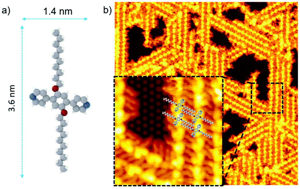 | ||
| Fig. 1 (a) Structural model of 1,4-di(4′,4′′-pyridyl)-2,5-bis(decyloxy)benzene PDB-OC10 molecule. Nitrogen atoms: blue, Oxygen atoms: red, Carbon atoms: grey, hydrogen atoms: white. (b) Large scale STM image (60 × 60 nm2, Vs = −1.3 V, It = 7 pA, T = 110 K) representing the self-assembled structure of PDB-OC10 molecules on Si(111)√3 × √3R30°-B substrate. The inset of the image corresponds to black dashed rectangular zoomed area (10 × 10 nm2, Vs = −1.3 V, It = 7 pA, T = 110 K) of supramolecular network on Si(111)√3 × √3R30°-B surface. | ||
PDB-OC10 molecule is based on a phenyl core terminating with two pyridyl moieties, distanced by 1.4 nm and further core-substituted with two lateral ether alkyl chains (Fig. 1a) containing 10 carbon atoms. The side chain lengths in PDB-OC10 is 3.6 nm. Fig. 1b and S1† (for a larger scale) show a high resolution STM image, recorded at 110 K, after the deposition of PDB-OC10 by thermal sublimation under ultra-high vacuum conditions on a Si(111)√3 × √3R30°-B substrate maintained at room temperature.
Well-organized stripes consisting of aligned pair of bright protrusions (length: 1.6 ± 0.1 nm) surrounded by slightly darker rods (length: 2.0 ± 0.2 nm), are observed. The stripes follow the three principal directions rotated by 120° of the substrate, surrounding the empty free space where the silicon adatoms are visible (inset of Fig. 1b). Consistent with the features of PDB-OC10, the bright protrusions can be attributed to the triphenyl cores of PDB-OC10 and the darker paired rods correspond to the interdigitated C10 alkyl chains of two PDB-OC10 molecules involved in two adjacent lines (Fig. 1b).13,16 Based on our STM observations and measurements, we obtain the adsorption model of the PDB-OC10/Si(111)√3 × √3R30°-B interface (see insert in Fig. 1b). With these results in hand, we were then interested in obtaining a better understanding of the reaction behaviour by scanning a large area of the PDB-OC10/Si(111)√3 × √3R30°-B network at a lower bias voltage. This result is representative of those obtained in repeated experiments for the bias voltage from −4.5 V to 0 V. Due to the molecule-molecule and molecule-surface interactions, the alkyl chains of PDB-OC10 molecules are always well visible in STM images. Notably, at the bias voltage of −4.5 V, we observed a remarkable modification of the PDB-OC10 molecules in STM images (see Fig. 2). The well-organized network is now disordered and the cross-shape of PDB-OC10 molecules disappeared. If the bias voltage is decreased beyond −4.5 V, the destruction of the original supramolecular network is still observed.
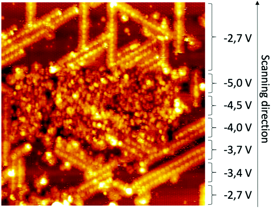 | ||
| Fig. 2 STM image captured while changing bias voltage during the scan shows significant modification of network at −4.5 V (60 × 60 nm2, Vs = variable values shown on image, It = 7 pA, T = 110 K). | ||
A further study of the effect of the bias voltage on the PDB-OC10/Si(111)√3 × √3R30°-B interface was then carried out. A 50 × 50 nm2 area was imaged by STM at Vs = −1.3 V, showing the typical STM image features of the PDB-OC10/Si(111)√3 × √3R30°-B interface (Fig. S2a†). Then, the same area was scanned at −4.5 V.
All the cross-shape corresponding to the PDB-OC10 molecules disappeared (Fig. S2b†), while Si(111)√3 × √3R30°-B surface is unaffected as shown by the uncovered area surrounded by dashed lines in Fig. S2b.† The same procedure was performed along a line of molecules, leading to the destruction of only the scanned line (Fig. S3†). Since the cross-shape of PDB-OC10 molecules is not visible, we moved the tip to another area of the PDB-OC10/Si(111)√3 × √3R30°-B interface, which have been previously scanned only at a voltage below −4.5 V, showing the ordered supramolecular network (Fig. 3a) constituted by entire PDB-OC10 molecules.
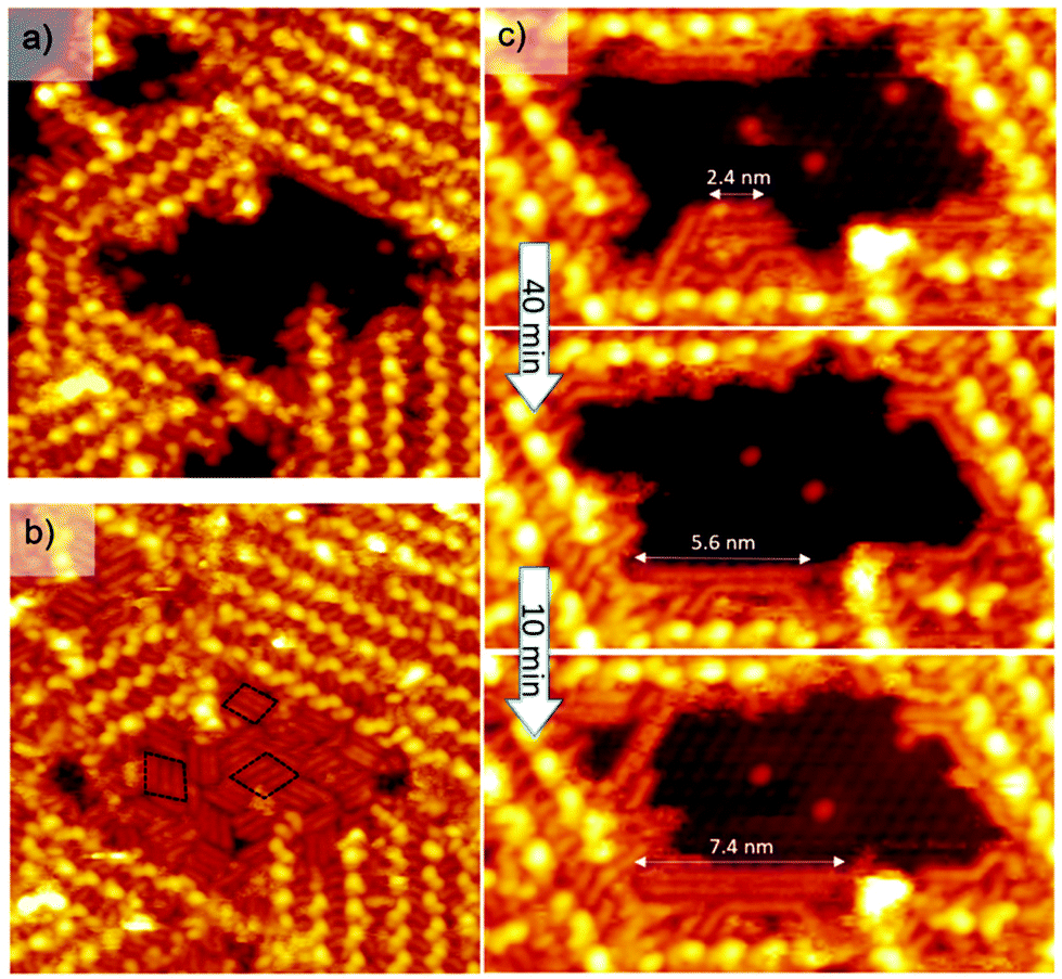 | ||
| Fig. 3 (a) STM image (25 × 25 nm2, Vs = −1.3 V, It = 7 pA, T = 110 K) representing a nano-pore inside the supramolecular network. (b) The same nano-pore fully filled with rod-like structures released by STM tip during scanning. (c) Three STM images (10 × 20 nm2, Vs = −1.3 V, It = 7 pA, T = 110 K) showing the growth of rod-like structures in a nanopore. | ||
This intact area is then scanned again at −1.3 V. During the scan, rod-like features appeared and filled the uncovered zone until it was completely covered by strips of parallel continuous rods (Fig. 3b). The rod-like features are arranged parallel in three different domains (see black dashed outlines on Fig. 3b) following the three symmetry axes of the Si(111)√3 × √3R30°-B surface. Based on the systematic analysis of more than 20 STM images, a statistical analysis of the size distribution of strips reveals a size repartition centered at a length of 2.1 nm (Fig. S4†). In addition, the length of these rod-like structures increases with time (Fig. 3c). Three STM images of the same area have been recorded after 40 and 50 minutes. The length of a rod structure increases from 2.4 nm to 7.4 nm while the number of small initial rods decreases. Finally, we have compared the profile of a C10 lateral alkyl chain of an entire PDB-OC10 molecule with the profile of a nanorod on the same STM image (Fig. S5†). These two profiles have the same shape and differ only by their length. On the basis of all these features, the rods are attributed to alkane oligomers adsorbed on the Si(111)√3 × √3R30°-B surface. The number of carbon atoms in the most common adsorbed alkane was 20 for a rod length of 2.1 ± 0.2 nm, respectively. In addition, the rod corresponding to decane (10 carbon atoms) and longer alkanes (like hexacontane, 60 carbon atoms 7.4 nm, Fig. 3c) were very rarely observed. The observation of the growth of long alkanes definitively indicates that a polymerization process occurs on the surface.
Discussion
The formation of oligomeric alkanes from aromatic species containing only ether side chains as precursors has not yet been reported in the literature. The resulting mechanism should involve at least two steps: (i) activation of the C–O bonds of the aromatic precursors at a fixed bias voltage and then (ii) on-surface oligomerisation of the generated species. For instance, the activation mechanism of C–O bonds in alkyl aryl ether derivatives has been extensively investigated in solution12 and most recently described by Yang et al. on noble metal surfaces.17 In the latter case, the authors suggested that the dealkylation process is based on a thermally-induced intramolecular prototropy from a hydrogen atom of the alkyl chain to the oxygen atom of the ether function. In solution, the dealkylation of aryl alkyl ethers can originate from a reduction (through an electron transfer12), or can be catalysed by a Lewis or Brønsted acid18 or by organometallic complexes (oxidative addition19). In our experiments, it is reasonable to rule out that the mechanism is based on a catalyst because no external catalytic species were introduced on the surface. Since the dealkylation reaction takes place even at low temperatures, a thermally-assisted mechanism is also unsuitable. As the transformation occurs at negative bias voltage, this involves electrons that tunnel from the substrate, through the adsorbed layer to the STM tip. Then, an electron originates from the valence band of the substate can be captured by low-lying energy empty states of PDB-OC10 molecule20 to generate an anion that relax through a dissociative electron attachment (DEA) mechanism.1g,21 The relaxation of that anion on the Si(111)√3 × √3R30°-B surface leads to the dissociation of PDB-OC10 into a phenoxide moiety and an alkyl radical. A similar reaction path was already demonstrated in the electrochemical reduction of cyanoanisole in solution.12 From DFT calculations, the electronic structure of PDB-OC10/Si(111)-B system shown in Fig. 4 supports such DEA mechanism for which the energy of empty states (mostly C-aromatic) above Fermi level (see Fig. 4(d)) are in the same energy range than the bias voltage used in STM experiments where the reaction occurs. Moreover, additional DFT calculations on gas phase species (see Fig. S6†) indicate that C–O bond breaking is easier on the aliphatic side than the aromatic side by around 1.8 eV per bond.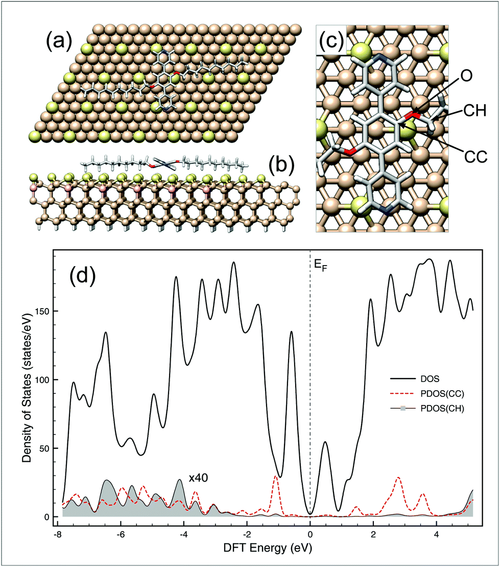 | ||
| Fig. 4 (a) Top view, (b) side view and (c) zoom view of the optimized supercell used to determine the electronic structure of PDB-OC10 adsorbed on Si(111)√3 × √3R30°-B surface by DFT. Clearly in (a), the C10 chains of PDB-OC10 (92 atoms) are well-aligned along Si-adatom rows that we have identified within the substrate (582 atoms) through brighter color for clarity. The density of states (DOS) and the projection (PDOS) profiles of the system are reported in (d) where the PDOS of aromatic (CC) and aliphatic carbon atom (CH) are the summed contribution of each species around O moieties, all projections are multiplied by 40. | ||
The cleavage efficiency is 100%, leading to complete disorganization of the initial supramolecular network. It is worth noting that after C–O bond activation, the resulting phenoxide moieties were rarely observed on the STM images. This may be explained by their low adsorption energies on the Si(111)√3 × √3R30°-B, leading to their desorption (Fig. S7†). A comparison of adsorption energy for both species on Si(111)-B obtained by DFT calculations also supports a weaker interaction of phenoxide than PDB-OC10 on the surface (see ESI Fig. S8†). The alkane derivatives only reappear as a periodic supramolecular network by scanning the uncovered areas of the Si(111)√3 × √3R30°-B surface (Fig. 3 and S9†). In addition, tip instabilities are observed during the scanning, indicated that molecules are adsorbed on the STM tip (Fig. S10†). These features indicate that (i) the STM tip can act as a reservoir of C10 alkyl radicals, which can be released on the surface and (ii) These C10 radicals are free to diffuse on the Si(111)√3 × √3R30°-B surface.
From a mechanistic point of view, the combination of electron-attachment (reduction) and C–O bond cleavage can be considered as the initiation step of a radical oligomerisation (Fig. 5).
 | ||
| Fig. 5 C–O bond activation and cleavage of PBD-OC10 molecule followed by oligomerisation of the ensuing alkyl radicals on a Si(111)√3 × √3R30°-B surface. (1) DEA process by electron attachment leading to the formation of a radical-anion at Vs < −4.5 V. C–O bond cleavage leading to the formation of a phenoxide anion and an alkyl radical. The combination of these two steps is the initiation step of the radical oligomerisation of alkyl chains. (2) Propagation of the radical oligomerisation. A chain-transfer reaction of radical leads to the growth of the length of produced alkanes. (3) Termination of the radical oligomerisation by two main mechanisms: combination between two radicals or disproportionation. | ||
Since the procedure of DEA manipulation leads to the collective formation of radicals by scanning large areas of the starting supramolecular network of PBD-OC10 molecules, the resulting radicals can react with each other by radical oligomerisation. The chain growth step is regulated by the rate of radical formation, as is the propagation step of a radical oligomerisation (Fig. 5). In contrast to oligomerisation in solution, alkyl radicals have to diffuse to react, limiting the possibilities of the substrates to react and explaining why only linear alkanes are observed. When alkanes are long, chain growth can be stopped by two main termination processes (Fig. 5). Since residual hydrogen gas is present in very low amount in the UHV chamber, an additional termination step that would involve a reaction of radicals with H2 was safely ruled out. The occurrence of this type of side reactions could explain the fairly modest lengths observed for the final alkanes. However, in agreement with previous observations, we considered that the 2D confined geometry could also favour certain reactions that are not usually observed. Due to the unique space confinement, the formation of linear oligomers of similar molecular weights can be controlled. This finding is consistent with the statistical analysis of the size distribution of alkanes adsorbed on Si(111)√3 × √3R30°-B surface and the step-by-step growth described in Fig. 3c, which correspond to monitoring of the propagation step by STM images.
Conclusions
In summary, we have used STM under UHV conditions and with some voltage application to initiate the synthesis of alkyl oligomers on a semiconductor surface. We have shown that the lack of reactivity of semiconductors with respect to a metal surface can be circumvented by using the STM-tip as an active role-player. Indeed, all these experiments clearly demonstrate that the observed transformations are triggered by a local dissociative electron (tunnelling) attachment and do not require any another “catalytic” role of surfaces. This allows the collective formation of electron-induced radicals that are able to cross-react in a controlled manner without adding any additives to produce alkyl oligomers. The origin of the experimentally observed selectivity towards oligomer products has been attributed to the 1D restriction of the reactive species along the surface. This tunnelling electron-induced radical oligomerization is a major step towards the fabrication of molecular electronic devices and novel nanomaterials.Conflicts of interest
There are no conflicts to declare.Acknowledgements
We thank Dr B. Grandidier (IEMN, Lille, France) and Dr M.-L. Bocquet (ENS, Paris, France) for fruitful discussions. The authors acknowledge the financial support from the French National Research Agency through contract OVATION (ANR-19-CE09-0020) and from the Pays de Montbéliard Agglomération. C.M.T. is grateful to the Institut Universitaire de France (IUF). A.R. acknowledges the support from the Natural Sciences and Engineering Research Council of Canada (NSERC), and he is grateful to Calcul Québec and Compute Canada for providing computational resources.References
- (a) L. Grill, M. Dyer, L. Lafferentz, M. V. Persson and S. Hecht, Nat. Nanotechnol., 2007, 2, 687 CrossRef CAS PubMed; (b) L. Cai, P. Ruffieux, R. Jaafar, M. Bieri, T. Braun, M. Blankenburg, A. P. Seitsonen, M. Saleh, X. Feng, K. Mullen and R. Fasel, Nature, 2010, 466, 470 CrossRef; (c) M. Matena, T. Riehm, M. Stöhr, T. A. Jung and L. H. Gade, Angew. Chem., Int. Ed., 2008, 47, 2414 CrossRef CAS PubMed; (d) P. A. Held, H. Fuchs and A. Studer, Chem. – Eur. J., 2017, 23, 5874 CrossRef CAS PubMed; (e) H. Sakaguchi, S. Song, T. Kojima and T. Nakae, Nat. Chem., 2017, 9, 57 CrossRef CAS; (f) N. Pvalicek, Z. Majzik, S. Collazos, G. Meyer, D. Perez, E. Guitian, D. Pena and L. Gross, ACS Nano, 2017, 11, 10768 CrossRef PubMed; (g) S. Kawai, H. Sang, L. Kantorovitch, K. Takahashi, K. Nozaki and S. Ito, Angew. Chem., 2020, 59, 10842 CrossRef CAS PubMed; (h) B. Yang, B. Dong and L. Chi, ACS Nano, 2020, 14, 6376 CrossRef CAS PubMed; (i) S. Clair and D. G. de Oteyza, Chem. Rev., 2019, 119, 4717 CrossRef CAS PubMed; (j) M. Lackinger, Chem. Commun., 2017, 53, 7872 RSC; (k) M. Di Giovannantonio and G. Contini, J. Phys.: Condens. Matter, 2018, 30, 093001 CrossRef; (l) A. Gourdon, On-surface Synthesis, Springer, Switzerland, 2016 Search PubMed.
- (a) S.-W. Hla, L. Bartels, G. Meyer and K.-H. Rieder, Phys. Rev. Lett., 2000, 85, 2777 CrossRef CAS PubMed; (b) A. Riss, S. Wickenburg, P. Gorman, L. Z. Tan, H.-Z. Tsai, D. G. de Oteyza, Y.-C. Chen, A. J. Bradley, M. M. Ugeda, G. Etkin, S. G. Louie, F. R. Fischer and M. F. Crommie, Nano Lett., 2014, 14, 2251 CrossRef CAS; (c) Y. Okawa and M. Aono, Nature, 2001, 409, 683 CrossRef CAS; (d) V. Verstraete, B. E. Hirsche, J. Greenwood and S. De Feyter, Chem. Commun., 2017, 53, 4207 RSC; (e) S. Zint, D. Ebeling, T. Sclöder, S. Ahles, D. Mollenhauer, H. A. Wegner and A. Schirmeisen, ACS Nano, 2017, 11, 4183 CrossRef CAS PubMed; (f) A. Sanchez-Grande, J. I. Urgel, A. Cahlik, J. Santos, S. Edalatmanesh, E. Rodriguez-Sanchez, K. Lauwaet, P. Mutombno, D. Nachtigallova, R. Nieman, H. Lischka, B. de la Torre, R. Miranda, O. Gröning, N. Martin, P. Jelinek and D. Ejica, Angew. Chem., 2020, 59, 17594 CrossRef CAS PubMed; (g) G. Galeotti, M. Fritton and M. Lackinger, Angew. Chem., Int. Ed., 2020, 59, 22785 CrossRef CAS.
- (a) F. Para, F. Bocquet, L. Nony, C. Loppacher, M. Féron, F. Chérioux, D. Z. Gao, F. F. Canova and M. B. Watkins, Nat. Chem., 2018, 10, 1112 CrossRef CAS PubMed; (b) R. Linder, P. Rahe, M. Kittelmann, A. Gourdon, R. Bechstein and A. Kuhnle, Angew. Chem., Int. Ed., 2014, 53, 7952 CrossRef; (c) C.-A. Palma, K. Diller, R. Berger, A. Welle, J. Bjork, J. l. Cabellos, D. J. Mowbray, A. C. Papageorgiou, N. P. Ivleva, S. Matich, E. Margapoti, R. NIessner, B. Menges, J. Reichert, X. Feng, H. J. Rader, F. Klappenberger, K. Mullen and J. V. Barth, J. Am. Chem. Soc., 2014, 136, 4651 CrossRef CAS PubMed.
- For instance, almost 40% of all polymers produced in the United States are produced by this mechanism.
- K. Matyjaszewski and N. V. Tsarevsky, Nat. Chem., 2009, 1, 276 CrossRef CAS and references therein.
- These methods include atom-transfer radical polymerization (ATRP) and stable free-radical polymerization (SFRP), which proceed with reversible termination, and reversible addition-fragmentation transfer (RAFT), which proceeds with reversible chain transfer. See for instance: (a) G. Moad and D. H. Solomon, The Chemistry of Radical Polymerization, Elsevier Science, Oxford, UK, 2nd edn, 2006 Search PubMed; (b) Handbook of Radical Polymerization, ed. K. Matyjaszewski and T. P. Davis, Wiley Interscience, New York, 2002 Search PubMed; (c) W. A. Braunecker and K. Matyjaszewski, Prog. Polym. Sci., 2007, 32, 93 CrossRef CAS.
- V. Sciannamea, R. Jérôme and C. Detrembleur, Chem. Rev., 2008, 108, 1104 CrossRef CAS.
- (a) M. Szwarc, M. Levy and R. Milkovich, J. Am. Chem. Soc., 1956, 78, 2656 CrossRef CAS; (b) M. Szwarc, Nature, 1956, 178, 1168 CrossRef CAS; (c) O. W. Webster, Science, 1991, 251, 887 CrossRef CAS PubMed; (d) S. K. Varshney, R. Jérôme, P. Bayard, C. Jacobs, R. Fayt and P. Teyssié, Macromolecules, 1991, 24, 4997 CrossRef CAS.
- C. Robert, F. de Montigny and C. M. Thomas, Nat. Commun., 2011, 2, 586 CrossRef and references therein.
- C. Robert and C. M. Thomas, Chem. Soc. Rev., 2013, 42, 9392 RSC and references therein.
- (a) B. Baris, V. Luzet, E. Duverger, P. Sonnet, F. Palmino and F. Chérioux, Angew. Chem., Int. Ed., 2011, 50, 4094 CrossRef CAS PubMed; (b) S. R. Wagner, R. R. Lunt and P. Zhang, Phys. Rev. Lett., 2013, 110, 086107 CrossRef PubMed; (c) G. Copie, F. Cléri, Y. Makoudi, C. Krzeminski, M. Berthe, F. Cherioux, F. Palmino and B. Grandidier, Phys. Rev. Lett., 2015, 114, 066101 CrossRef CAS PubMed; (d) Y. Makoudi, J. Jeannoutot, F. Palmino, F. Cherioux, G. Copie, C. Krzeminski, F. Cléri and B. Grandidier, Surf. Sci. Rep., 2017, 72, 316 CrossRef CAS.
- (a) M. D. Koppang, N. F. Woosley and D. E. Bartak, J. Am. Chem. Soc., 1984, 106, 2799 CrossRef CAS; (b) L. Testaferri, M. Tiecco, M. Tingoli, D. Chianelli and M. Montanuc, Tetrahedron, 1982, 38, 3687 CrossRef CAS.
- Y. Makoudi, M. Beyer, S. Lamare, J. Jeannoutot, F. Palmino and F. Chérioux, Nanoscale, 2016, 8, 12347 RSC.
- (a) A. Amrous, F. Bocquet, L. Nony, F. Para, C. Loppacher, S. Lamare, F. Palmino, F. Chérioux, D. Z. Gao, F. F. Canova, M. B. Watkins and A. L. Shluger, Adv. Mater. Interfaces, 2014, 1, 1400414 CrossRef.
- G. Zhan, M.-A. Dubois, Y. Makoudi, S. Lamare, J. Jeannoutot, X. Bouju, A. Rochefort, F. Palmino and F. Chérioux, J. Phys. Chem. C, 2017, 121, 8427 CrossRef CAS.
- T. Kudernac, S. Lei, J. A. A. W. Elemans and S. De Feyter, Chem. Soc. Rev., 2009, 38, 402 RSC.
- B. Yang, H. Lin, K. Miao, P. Zhu, L. Liang, K. Sun, H. Zhang, J. Fan, V. Meunier, Y. Li, Q. Li and L. Chi, Angew. Chem., Int. Ed., 2016, 55, 9881 CrossRef CAS PubMed.
- M. Tobisu and N. Chatani, Acc. Chem. Res., 2015, 48, 1717 CrossRef CAS PubMed.
- S. A. Weissman and D. Zwege, Tetrahedron, 2005, 61, 7833 CrossRef CAS.
- (a) W. Chen, D. Qi, X. Gao and A. T. S. Wee, Prog. Surf. Sci., 2009, 84, 270 CrossRef; (b) S. R. Wagner, B. Huang, C. Park, J. Feng, M. Yoon and P. Zhang, Phys. Rev. Lett., 2015, 115, 096101 CrossRef PubMed; (c) S. Lindner, M. Franz, M. Kubicki, S. Appelfeller, M. Dähne and H. Eisele, Phys. Rev. B, 2019, 100, 245301 CrossRef CAS; (d) R. G. A. Veiga, R. H. Miwa and A. B. McLean, Phys. Rev. B, 2016, 93, 115301 CrossRef; (e) N. P. Guisinger, M. E. Greene, R. Basu, A. S. Baluch and M. C. Hersam, Nano Lett, 2004, 4, 55 CrossRef CAS; (f) M. Kubicki, S. Lindner, M. Franz, H. Eisele and M. Dähne, J. Vac. Sci. Technol., B: Nanotechnol. Microelectron.: Mater., Process., Meas., Phenom., 2020, 38, 042803 CAS.
- (a) M. Stepanovic, Y. Parlay and M. Allan, J. Chem. Phys., 1999, 110, 11376 CrossRef CAS; (b) C. Bulliard, M. Allan and S. Grimme, Int. J. Mass Spectrom., 2001, 205, 43 CrossRef CAS; (c) R. Martel, P. Avouris and I.-W. Lyo, Science, 1996, 272, 385 CrossRef CAS.
Footnote |
| † Electronic supplementary information (ESI) available: Synthetic procedure, DFT calculations details and additional STM images. See DOI: 10.1039/d0nr08291k |
| This journal is © The Royal Society of Chemistry 2021 |