
 Open Access Article
 This Open Access Article is licensed under a
 Creative Commons Attribution 3.0 Unported Licence
Single-step chemical vapour deposition of anti-pyramid MoS2/WS2 vertical heterostructures†
Xueyin
Bai
 *a,
Shisheng
Li
b,
Susobhan
Das
a,
Luojun
Du
a,
Yunyun
Dai
a,
Lide
Yao
c,
Ramesh
Raju
a,
Mingde
Du
a,
Harri
Lipsanen
a and
Zhipei
Sun
ad
*a,
Shisheng
Li
b,
Susobhan
Das
a,
Luojun
Du
a,
Yunyun
Dai
a,
Lide
Yao
c,
Ramesh
Raju
a,
Mingde
Du
a,
Harri
Lipsanen
a and
Zhipei
Sun
ad
aDepartment of Electronics and Nanoengineering, Aalto University, Finland. E-mail: xueyin.bai@aalto.fi
bInternational Center for Young Scientists (ICYS), National Institute for Materials Science (NIMS), Japan
cDepartment of Applied Physics, Aalto University, Finland
dQTF Centre of Excellence, Department of Applied Physics, Aalto University, Finland
First published on 2nd February 2021
Abstract
Van der Waals heterostructures are the fundamental building blocks of electronic and optoelectronic devices. Here we report that, through a single-step chemical vapour deposition (CVD) process, high-quality vertical bilayer MoS2/WS2 heterostructures with a grain size up to ∼60 μm can be synthesized from molten salt precursors, Na2MoO4 and Na2WO4. Instead of normal pyramid vertical heterostructures grown by CVD, this method synthesizes an anti-pyramid MoS2/WS2 structure, which is characterized by Raman, photoluminescence and second harmonic generation microscopy. Our facile CVD strategy for synthesizing anti-pyramid structures unveils a new synthesis route for the products of two-dimensional heterostructures and their devices for application.
1. Introduction
Two-dimensional (2D) materials are a series of crystalline materials with a thickness at atomic scale, such as graphene, transition metal dichalcogenides (TMDs), hexagonal boron nitride (h-BN) and other materials. Due to their unique properties, these 2D materials are expected to play important roles in future electronics, optoelectronics and photonics.1–6 By vertically stacking different 2D materials, various 2D van der Waals heterostructures (2D heterostructures) have been demonstrated showing improved performance or even completely novel properties, and potential for various applications.7–10 For example, by the stacking of graphene, h-BN and MoS2 as a heterostructure, Withers et al. have achieved light emitting diodes with a quantum efficiency of 8.4%,11 while monolayer MoS2 based light emitting diodes typically only have that of less than 1%.12,13 Hence, 2D heterostructures are very attractive to researchers, and how to obtain scalable and high-quality heterostructures and their devices is an important question urgently waiting for answers.In the synthesis of 2D materials and their heterojunctions, chemical vapour deposition (CVD) is a common and facile method due to its best balance between scalable and controllable growth, high quality and large area production, and economic cost.10,14 Lots of efforts have been made to synthesize various TMDs, including single or multilayer (homo)structure and heterostructure stacking with different TMD layers. Usually, a heterostructure is fabricated by a multi-step CVD growth method, in which two or more different precursors are injected into the system in sequence.15–18 The only single-step process, to the best of our knowledge, is a reported growth method of a WS2/MoS2 heterostructure, in which additional tellurium is added as a promoter to accelerate the melting of tungsten powder.19 Nevertheless, similar to other CVD growth methods,20 transition metals in this work are offered as a vapour of metal oxides, leading to difficulties in controlling the thickness and size of TMDs. Hence, finding a facile fabrication method for the heterostructure which consists of monolayer TMDs is still challenging. Recently, Li et al. demonstrated a novel vapour–liquid–solid (VLS) growth method of TMDs.21,22 In sharp contrast to the vapour of transition metal oxides in other growth methods, the non-volatile salts, e.g., Na2MoO4 and Na2WO4, used in the VLS growth method are in the liquid phase during the reaction, yielding solid monolayer TMDs after being saturated with chalcogens. This VLS growth method has been proved as a promising method for synthesizing various monolayer TMDs with a large area and high quality.21–23 However, to date, no heterostructures have been demonstrated by this process.
In this work, by carefully choosing the precursors, we demonstrated a versatile, reproducible one-step growth method for the 2D TMD heterostructures without any additional promoters. This is the first report of fabrication of a vertical anti-pyramid heterostructure by the CVD growth method. The synthesized MoS2/WS2 heterostructure has a lateral grain size of up to 60 μm and a structure of AA′ stacking. Optical microscopy, micro-Raman and photoluminescence (PL) spectroscopy, atomic force microscopy (AFM), as well as non-linear optical spectroscopy are used to fully characterize the structural and optical qualities of the as-synthesized heterostructures.
2. Results and discussion
To grow the MoS2/WS2 heterostructure, 5 mg mL−1 Na2MoO4 and Na2WO4 are firstly spin-coated on two sapphire or SiO2/Si substrates, respectively. Then, the two substrates with the precursors are placed in a dual-zone tube furnace side by side, as illustrated in Fig. 1a. Meanwhile, ∼100 mg sulphur is loaded at the centre of Zone 1 in upstream. 70 sccm Ar is chosen as the carrier gas. The temperature ramping rate of Zone 2 is 10 °C min−1. When Zone 2 reaches the growth temperature (825 °C for sapphire and 775 °C for SiO2/Si), the temperature of Zone 1 reaches 200 °C for sulphur evaporation. Both zones are stabilized for 10 min and cooled to room temperature naturally. The MoS2/WS2 heterostructure is only grown on the substrate with Na2WO4, while the substrate with Na2MoO4 has only triangular flakes of MoS2 (Fig. S2†). Some typical optical images of MoS2/WS2 heterostructures are shown in Fig. 1b. The dark triangular centre of the flakes is considered as the MoS2/WS2 heterostructure region, exhibiting a typical 3-fold symmetry with straight edges. The lateral size of the heterostructure is up to 60 μm.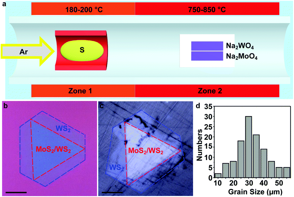 | ||
| Fig. 1 Schematic illustration of the growth setup and optical images of the MoS2/WS2 heterostructures. (a) Schematic illustration of the growth system. (b and c) Typical optical microscopy images of the synthesized MoS2/WS2 heterostructures on SiO2/Si (b) and sapphire (c) substrates, respectively (scale bar, 20 μm). (d) A histogram of grain sizes from 124 heterostructures from randomly selected areas of the sample. | ||
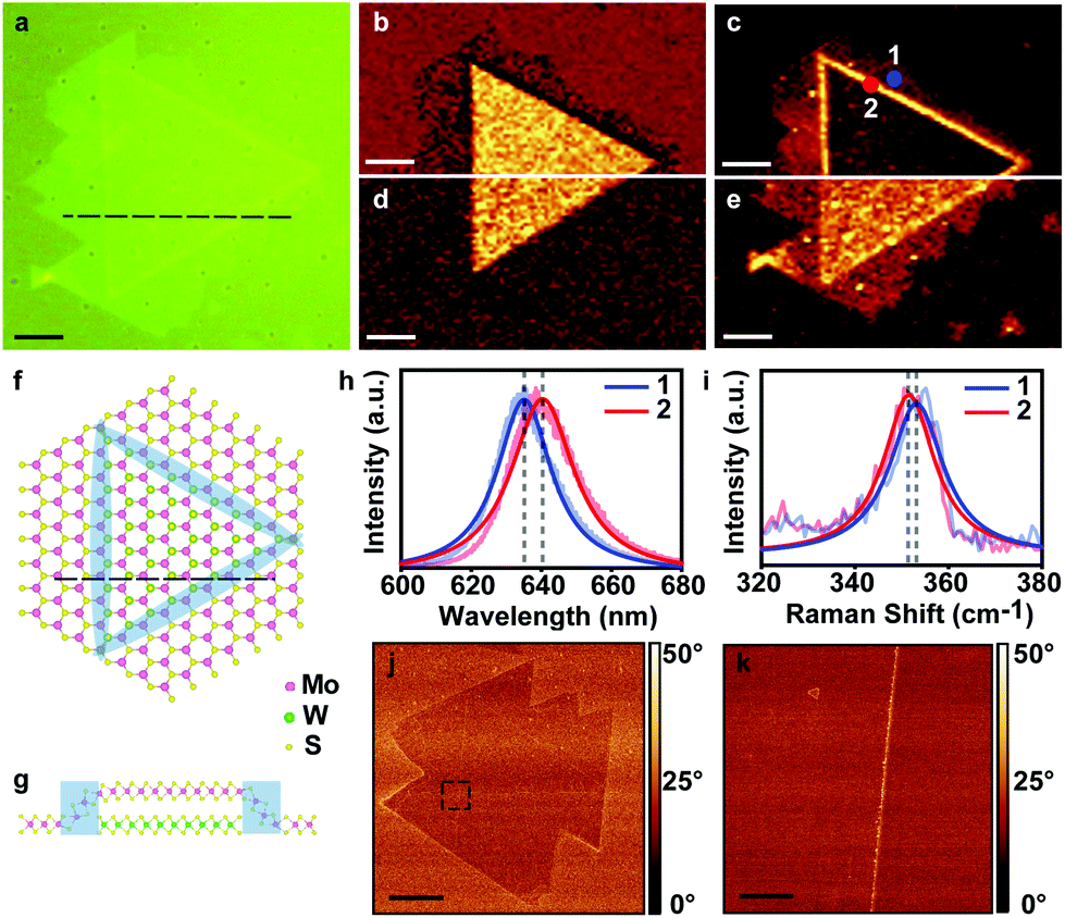
Raman and PL spectroscopy are usually used for determining the thickness and composition of TMDs and their heterostructures. Here, we measure the Raman and PL spectra of two different heterostructures, as shown in Fig. 2a and d, respectively. It is noticeable that the flake in Fig. 2a has two different parts, a dark triangular bilayer and a surrounding monolayer. The Raman and PL spectra of the bilayer (black dot in Fig. 2a) show 4 typical peaks (black curve in Fig. 2b). The two peaks at 385 cm−1 and 404 cm−1 are assigned to the E2g and A1g mode phonons of monolayer MoS2, while the other two peaks, 351 cm−1 and 417 cm−1, are indicated to be the 2LA(M) + E2g and A1g phonon modes of WS2.24,25 With the Raman spectrum (black curve in Fig. 2b), it is concluded that the dark triangular centre is a composite of MoS2 and WS2 monolayers. Meanwhile, the Raman spectrum (blue curve in Fig. 2b) measured at the blue dot of Fig. 2a only shows peaks at 351 cm−1 and 417 cm−1, indicating that the light outside part is the WS2 monolayer. For the PL measurements, two PL peaks with centres at 670 nm and 620 nm are observed with a magnification of 50 times from the black dot, indicating that the peaks are the A and B excitons of the monolayer MoS2, respectively. In addition, the extremely weak peaks also indicate that the transfer of electrons and holes happens during the PL measurements,9 which agrees with the MoS2/WS2 heterostructures. At the blue dot, the high-intensity PL peak with a centre at 630 nm is assigned to the A exciton of the monolayer WS2 and indicates that the light outside part is the monolayer WS2. Therefore, the flake in Fig. 2a is confirmed as a heterostructure with the monolayer MoS2 (area in red dashed lines) and the monolayer WS2 (area in blue dashed lines).
 | ||
| Fig. 2 Optical characterization of the MoS2/WS2 heterostructure. (a) Optical microscopy images of the heterostructures (scale bar, 10 μm). (b) Raman and (c) PL spectra at the marked dots with the same colours, respectively (black PL spectrum with 50 times magnification). (d) Optical microscopy images of a partial stacking heterostructure (scale bar, 25 μm). (e) Raman and (f) PL spectra at the marked dots with the same colours, respectively (black PL spectrum with 50 times magnification). | ||
To exclude other possibilities (e.g., MoS2/WS2 alloy), a special heterostructure shown in Fig. 2d is found on the substrate and is measured to clarify the structure. The flake shows a partial stacking by two layers marked with red and blue dashed lines, respectively. In the PL and Raman spectra at the left part of the monolayer (red dot), two phonon modes at 385 cm−1 and 404 cm−1 and a luminescence peak at 670 nm are observed, as shown in Fig. 2e and f, indicating that the left part (i.e., the red dotted area of Fig. 2d) is monolayer MoS2. Similarly, the luminescence at 630 nm and the phonon modes at 351 cm−1 and 417 cm−1 at the right part of the monolayer (blue dotted area in Fig. 2d) indicate that it is monolayer WS2. Note that the PL and phonon modes measured at the black dot in Fig. 2d are very similar to the results measured at the black dot in Fig. 2a. Considering the left and right parts are MoS2 and WS2 monolayers, respectively, the middle part is believed to be a vertical stacking part of the MoS2 and WS2 monolayers. Hence, we firmly conclude that our product is a MoS2/WS2 heterostructure composed of monolayer MoS2 and monolayer WS2.
The vertical stacking order of our MoS2/WS2 heterostructure is important for understanding the formation mechanism and finding future applications. To clarify the vertical stacking order, Raman spectroscopy is employed to study a typical MoS2/WS2 heterostructure (Fig. 3a). Our heterostructure shows an abnormal enhancement in the Raman intensity mapping using a 532 nm laser. Fig. 3b and c show the intensity mapping of the E2g mode of MoS2 (385 cm−1) and E2g and 2LA(M) modes of WS2 (351 cm−1), respectively. A clear enhanced intensity of 2LA(M) + E2g modes is observed at the edges of the MoS2/WS2 heterostructure, which is not observed when using a 488 nm laser (Fig. 3e). The enhancement is related to the lattice deformation of the top WS2 layer, as shown by the top-view and cross-section schematic illustration in Fig. 3f and g, respectively. According to the theoretical calculations and experimental reports,26–28 the lattice deformation of the monolayer WS2 leads to an obvious and coincident adjustment of the electronic band structure. As a result, both the direct transition energy gap at the K point and the indirect transition energy gap at the M point of the Brillouin zone are narrowed and this leads to a reduction of the photon energy as well as a redshift of the peak positions of the A and B excitons. Meanwhile, as the 2LA(M) mode intensity is related to the resonance coupling between the B exciton and the 532 nm exciton laser, the shift of the B exciton leads to the enhancement of the 2LA(M) intensity.25Fig. 3h and i show the normalized PL and Raman spectra and their Lorentzian fitting curves, respectively, at the marked positions in Fig. 3c. Both PL and Raman spectra clearly show a red shift confirming our discussion of the lattice deformation. Besides, from the AFM phase analysis shown in Fig. 3i and j, no different phase angle is observed between the central triangular part and the outside hexagonal part, indicating that the two parts have the same surface. Otherwise, a clear contrast between the two different TMDs should occur.29 Since the outside part has already been confirmed to be the WS2 monolayer by Raman microscopy, the top layer of the heterostructure is the monolayer of WS2. We also have compared these results with an artificial anti-pyramid heterostructure made from a monolayer WS2 flake overlapping on a triangular MoS2 flake (Fig. S5†). In comparison, we notice that both enhanced Raman intensity and AFM phase coherence exist in both the artificial heterostructure and our as-grown heterostructure, which indicates that our synthesized heterostructure has the same anti-pyramid structure as that of the artificial heterostructure. Hence, it is fully confirmed that the top layer of the MoS2/WS2 heterostructures is monolayer WS2 and the bottom layer is MoS2, implying that the heterostructure is an anti-pyramid structure. In the previous studies of multilayer homo- or heterostructures, the most common stacking order is the pyramid order, in which a smaller layer lies on a bigger layer forming a pyramid structure. Meanwhile, the opposite order, anti-pyramid order, is rarely reported. However, the anti-pyramid order is more important, in which part of the top layer ignores the borders of the bottom layer. Therefore, this method has the possibility to make the flake free-standing, contributing to the study of physical properties without the influence of the substrates. Besides, due to the existence of MoS2 underneath, the central part of WS2 will have a different dielectric environment from the outside part, which contacts with the SiO2/Si substrate. This difference in the environment could lead to a dielectric induced band-gap renormalization effect, which could be used to form a lateral electronic junction with atomic scales in the WS2 layer.30 Such a diode-like junction has a strong asymmetric behaviour, which can provide a new approach for engineering 2D nanoelectronic devices.31
 | ||
| Fig. 3 The enhanced Raman intensity mapping and AFM phase images. (a) Optical image of the MoS2/WS2 heterostructure (scale bar: 10 μm). (b–e) Raman intensity mapping at 385 cm−1 (b) and 351 cm−1 (c) using a 532 nm laser as well as at 385 cm−1 (d) and 351 cm−1 (e) using a 488 nm laser (scale bar: 10 μm). (f) Atomic schematic illustration of the flake shown in (a). (g) Cross-section at the dashed line in (f). (h) Normalized PL spectra (light blue and red) and their Lorentzian fitting curves (blue and red) at the marked positions in (c). (i) Normalized Raman spectra at 2LA(M) + E2g modes (light blue and red) and their Lorentzian fitting curves (blue and red) at the marked positions in (c). (j) AFM phase image of a typical heterostructure (scale bar: 10 μm). (k) High resolution AFM phase image of the dashed line area in (j) (scale bar: 1 μm). | ||
Second harmonic generation microscopy (SHG) is also used to demonstrate the symmetric stacking of the heterostructure. For monolayer TMDs such as MoS2 and WS2, transition metal atoms and sulphur atoms form an asymmetric “hexatomic” ring without any symmetry centre and lead to a six-petal polarization pattern, as shown in Fig. 4a (left). When monolayer MoS2 and monolayer WS2 stack with an angle of 60° (known as AA′ stacking), the Mo atoms of MoS2 are stacked on the S atoms of WS2 and the S atoms of MoS2 are stacked on the W atoms of WS2, leading to a slight increase of centrosymmetry and a decrease of SHG intensity, as shown in Fig. 4a (right). The measured SHG intensity of the heterostructure is shown in Fig. 4b, and it is clear that the SHG of the MoS2/WS2 heterostructure has the same orientation as that of WS2 outside with a lower intensity, indicating that the MoS2/WS2 heterostructure has AA′ stacking. Besides, the total SHG intensity in the heterostructure with an angle between the two layers, Ih(θ), can be expressed as:32,33
Ih(θ) ∝ (χ1(2))2 + (χ2(2))2 + 2|χ1(2)||χ2(2)|cos![[thin space (1/6-em)]](https://www.rsc.org/images/entities/char_2009.gif) 3θ, 3θ, | (1) |
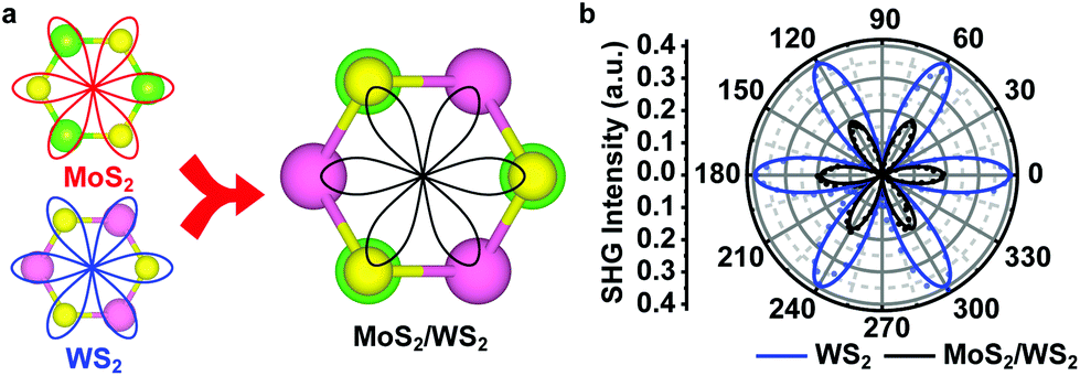 | ||
| Fig. 4 Second harmonic generation of the MoS2/WS2 heterostructure. (a) Schematic illustration of second harmonic generation on MoS2, WS2 and MoS2/WS2. (b) Measured second harmonic generation intensity of the WS2 part (blue) and MoS2/WS2 part (black). | ||
After understanding the stacking of heterostructures, it is worth discussing how the formation of AA′-stacking anti-pyramid MoS2/WS2 heterostructures occurs. Control experiments, in which blank substrates are used instead of a substrate with Na2MoO4 or Na2WO4, respectively, are carried out at the same temperature of the heterostructure growth. Triangular MoS2 flakes are formed on the blank substrate side-by-side with Na2MoO4, while no WS2 flakes are observed in another blank substrate with Na2WO4, as shown in Fig. S6 and S7,† indicating the diffusion of Na2MoO4 and no diffusion of Na2WO4 at the growth temperature. Based on this and the different temperatures between MoS2 and WS2 growth, the heterostructure formation process is shown in the schematic illustration in Fig. 5 using the as-grown sample on a SiO2/Si substrate as an example. At 700–800 °C, the melting Na2MoO4 transforms into a gas phase, diffuses to the substrate with Na2WO4, then dissolves in melting Na2WO4 and finally forms a liquid mixture. Later, with the dissolving of sulphur gas in the mixture droplets, MoS2 starts to nucleate because it can grow at a lower temperature, 700 °C and forms triangular MoS2 flakes with S-terminal zig-zag edges. Then, the increasing temperature, 775 °C, leads to the nucleation and growth of WS2. The selective growth of WS2 on MoS2 is caused by the larger energy barrier, which makes the absorbed WS2 more immobile, facilitating nucleation and growth on MoS2.35 Based on the results of different theoretical calculations,36–38 it is seen that the most stable stacking of 2-layer TMDs is AA′ stacking, which is the same in our heterostructures as demonstrated. In this structure, the top layer WS2 stacks on the bottom layer MoS2 with an orientation of difference 60°, which makes the Klein edges of WS2 have the same epitaxial direction as that of the zig-zag edges of MoS2. According to the previous research,39 the growth kinetics of zig-zag edges and Klein edges are different and the Klein edges grow epitaxially much more faster. Because of the fast epitaxy, the Klein edges of WS2 are able to extend without the limitation of MoS2 boundaries and the anti-pyramid heterostructures are obtained finally. However, due to the lack of the tungsten precursor, WS2 grows to a hexagonal structure with incomplete and uneven edges instead of the triangular structure. Nevertheless, here, the WS2/MoS2 heterostructure growth can be fully understood.
 | ||
| Fig. 5 Schematic illustration of the heterostructure epitaxy. (a) MoS2 nucleation. (b) MoS2 epitaxy. (c) MoS2 triangular flake formation. (d) WS2 nucleation on the MoS2 layer. (e) WS2 epitaxy on the MoS2 layer. (f) WS2 epitaxy outside the MoS2 layer. (g) MoS2/WS2 heterostructure formation. | ||
3. Conclusion
In conclusion, we report a facile and reproducible single-step CVD method for growing vertical bilayer MoS2/WS2 heterostructures with a lateral size up to ∼60 μm. In this method, no additional chemical is required, and a relatively low growth temperature is needed, compared with other single-step MoS2/WS2 growth processes. In addition, the AA′-stacking with an anti-pyramid order is demonstrated by different techniques, including Raman, PL, AFM and SHG microscopy. The novel anti-pyramid order indicates that the VLS process has the potential for ignoring the borders of the substrate and forming free-standing TMDs. This method offers an opportunity to synthesize heterostructures in a simple but efficient way. It could also possibly provide a potential strategy for devices based on free-standing 2D materials and a new approach for engineering 2D nanoelectronic devices.4. Experimental
Na2MoO4 (99.9%, Sigma-Aldrich) and Na2WO4 (99.995%, Sigma-Aldrich) are used as purchased. Si substrates with 280 nm thick SiO2 are purchased from University Wafer and cleaned with acetone and isopropanol, followed by O2 plasma treatment before use. The growth occurs in a dual-zone tube furnace (MTI Corp.). Ar (99.995%, Agar) is chosen as the carrier gas.Raman spectra are recorded using a WITec alpha300 RA+ system with a 532 nm or 488 nm continuous wave laser. SHG spectra are recorded using a femtosecond laser (Spectra-Physics, TOPAS) at a wavelength of 800 nm (repetition rate: 2 kHz). The pulse duration of the laser pulse is ∼230 fs. AFM topographic and phase images are obtained using an AFM Dimension Icon (Bruker) with a tapping mode.
Conflicts of interest
There are no conflicts to declare.Acknowledgements
The authors thank the provision of facilities and technical support by Aalto University at the OtaNano-Micronova Nanofabrication Centre and OtaNano-Nanomicroscopy Center (Aalto-NMC). The authors also acknowledge the support from the Academy of Finland (Grant No. 314810, 333982, 336144 and 336818), the Academy of Finland Flagship Programme (Grant No. 320167, PREIN), the European Union's Horizon 2020 Research and Innovation Program (Grant No. 820423, S2QUIP) and the European Research Council (Grant No. 834742).References
- Z. Sun, A. Martinez and F. Wang, Nat. Photonics, 2016, 10, 227–238 CrossRef CAS.
- A. C. Ferrari, F. Bonaccorso, V. Fal'Ko, K. S. Novoselov, S. Roche, P. Bøggild, S. Borini, F. H. Koppens, V. Palermo and N. Pugno, et al. , Nanoscale, 2015, 7, 4598–4810 RSC.
- J. Shim, H.-Y. Park, D.-H. Kang, J.-O. Kim, S.-H. Jo, Y. Park and J.-H. Park, Adv. Electron. Mater., 2017, 3, 1600364 CrossRef.
- X. Li, L. Tao, Z. Chen, H. Fang, X. Li, X. Wang, J.-B. Xu and H. Zhu, Appl. Phys. Rev., 2017, 4, 021306 Search PubMed.
- W. Zhang, Q. Wang, Y. Chen, Z. Wang and A. T. Wee, 2D Mater., 2016, 3, 022001 CrossRef.
- J. Wang, I. Verzhbitskiy and G. Eda, Adv. Mater., 2018, 30, 1802687 CrossRef.
- P. Xiong, R. Ma, N. Sakai, L. Nurdiwijayanto and T. Sasaki, ACS Energy Lett., 2018, 3, 997–1005 CrossRef CAS.
- P. Xiong, X. Zhang, H. Wan, S. Wang, Y. Zhao, J. Zhang, D. Zhou, W. Gao, R. Ma and T. Sasaki, et al. , Nano Lett., 2019, 19, 4518–4526 CrossRef CAS.
- K. Novoselov, A. Mishchenko, A. Carvalho and A. C. Neto, Science, 2016, 353, aac9439 CrossRef CAS.
- Z. Cai, B. Liu, X. Zou and H.-M. Cheng, Chem. Rev., 2018, 118, 6091–6133 CrossRef CAS.
- F. Withers, O. Del Pozo-Zamudio, A. Mishchenko, A. Rooney, A. Gholinia, K. Watanabe, T. Taniguchi, S. Haigh, A. Geim and A. Tartakovskii, et al. , Nat. Mater., 2015, 14, 301–306 CrossRef CAS.
- R. Sundaram, M. Engel, A. Lombardo, R. Krupke, A. Ferrari, P. Avouris and M. Steiner, Nano Lett., 2013, 13, 1416–1421 CrossRef CAS.
- E. Ponomarev, I. Gutiérrez-Lezama, N. Ubrig and A. F. Morpurgo, Nano Lett., 2015, 15, 8289–8294 CrossRef CAS.
- Y. Zhang, Y. Yao, M. G. Sendeku, L. Yin, X. Zhan, F. Wang, Z. Wang and J. He, Adv. Mater., 2019, 31, 1901694 CrossRef CAS.
- Q. Zhang, X. Xiao, R. Zhao, D. Lv, G. Xu, Z. Lu, L. Sun, S. Lin, X. Gao and J. Zhou, et al. , Angew. Chem., Int. Ed., 2015, 54, 8957–8960 CrossRef CAS.
- X. Zhou, N. Zhou, C. Li, H. Song, Q. Zhang, X. Hu, L. Gan, H. Li, J. Lü and J. Luo, et al. , 2D Mater., 2017, 4, 025048 CrossRef.
- Y. Gong, S. Lei, G. Ye, B. Li, Y. He, K. Keyshar, X. Zhang, Q. Wang, J. Lou and Z. Liu, et al. , Nano Lett., 2015, 15, 6135–6141 CrossRef CAS.
- T. Yang, B. Zheng, Z. Wang, T. Xu, C. Pan, J. Zou, X. Zhang, Z. Qi, H. Liu and Y. Feng, et al. , Nat. Commun., 2017, 8, 1906 CrossRef.
- Y. Gong, J. Lin, X. Wang, G. Shi, S. Lei, Z. Lin, X. Zou, G. Ye, R. Vajtai and B. I. Yakobson, et al. , Nat. Mater., 2014, 13, 1135–1142 CrossRef CAS.
- K. Bogaert, S. Liu, J. Chesin, D. Titow, S. Gradecak and S. Garaj, Nano Lett., 2016, 16, 5129–5134 CrossRef CAS.
- S. Li, Y.-C. Lin, W. Zhao, J. Wu, Z. Wang, Z. Hu, Y. Shen, D.-M. Tang, J. Wang and Q. Zhang, et al. , Nat. Mater., 2018, 17, 535–542 CrossRef CAS.
- S. Li, Y.-C. Lin, X.-Y. Liu, Z. Hu, J. Wu, H. Nakajima, S. Liu, T. Okazaki, W. Chen and T. Minari, et al. , Nanoscale, 2019, 11, 16122–16129 RSC.
- J. Zhou, J. Lin, X. Huang, Y. Zhou, Y. Chen, J. Xia, H. Wang, Y. Xie, H. Yu and J. Lei, et al. , Nature, 2018, 556, 355–359 CrossRef CAS.
- H. Li, Q. Zhang, C. C. R. Yap, B. K. Tay, T. H. T. Edwin, A. Olivier and D. Baillargeat, Adv. Funct. Mater., 2012, 22, 1385–1390 CrossRef CAS.
- F. Wang, I. A. Kinloch, D. Wolverson, R. Tenne, A. Zak, E. O'Connell, U. Bangert and R. J. Young, 2D Mater., 2016, 4, 015007 CrossRef.
- J. Feng, X. Qian, C.-W. Huang and J. Li, Nat. Photonics, 2012, 6, 866–872 CrossRef CAS.
- C. Zhu, G. Wang, B. Liu, X. Marie, X. Qiao, X. Zhang, X. Wu, H. Fan, P. Tan and T. Amand, et al. , Phys. Rev. B: Condens. Matter Mater. Phys., 2013, 88, 121301 CrossRef.
- M. Zeng, J. Liu, L. Zhou, R. G. Mendes, Y. Dong, M.-Y. Zhang, Z.-H. Cui, Z. Cai, Z. Zhang and D. Zhu, et al. , Nat. Mater., 2020, 19, 528–533 CrossRef CAS.
- C.-Y. Lin, X. Zhu, S.-H. Tsai, S.-P. Tsai, S. Lei, Y. Shi, L.-J. Li, S.-J. Huang, W.-F. Wu and W.-K. Yeh, et al. , ACS Nano, 2017, 11, 11015–11023 CrossRef CAS.
- F. Giannazzo, Nat. Electron., 2019, 2, 54–55 CrossRef.
- M. I. B. Utama, H. Kleemann, W. Zhao, C. S. Ong, H. Felipe, D. Y. Qiu, H. Cai, H. Li, R. Kou and S. Zhao, et al. , Nat. Electron., 2019, 2, 60–65 CrossRef CAS.
- W.-T. Hsu, Z.-A. Zhao, L.-J. Li, C.-H. Chen, M.-H. Chiu, P.-S. Chang, Y.-C. Chou and W.-H. Chang, ACS Nano, 2014, 8, 2951–2958 CrossRef CAS.
- A. Autere, H. Jussila, Y. Dai, Y. Wang, H. Lipsanen and Z. Sun, Adv. Mater., 2018, 30, 1705963 CrossRef.
- A. Autere, H. Jussila, A. Marini, J. Saavedra, Y. Dai, A. Säynätjoki, L. Karvonen, H. Yang, B. Amirsolaimani and R. A. Norwood, et al. , Phys. Rev. B, 2018, 98, 115426 CrossRef CAS.
- J. Zhu, W. Li, R. Huang, L. Ma, H. Sun, J.-H. Choi, L. Zhang, Y. Cui and G. Zou, J. Am. Chem. Soc., 2020, 142, 16276–16284 CrossRef CAS.
- A. Blumberg, U. Keshet, I. Zaltsman and O. Hod, J. Phys. Chem. Lett., 2012, 3, 1936–1940 CrossRef CAS.
- Q. Liu, L. Li, Y. Li, Z. Gao, Z. Chen and J. Lu, J. Phys. Chem. C, 2012, 116, 21556–21562 CrossRef CAS.
- T. Peng, G. Huai-Hong, Y. Teng and Z. Zhi-Dong, Chin. Phys. B, 2014, 23, 106801 CrossRef.
- D. Zhu, H. Shu, F. Jiang, D. Lv, V. Asokan, O. Omar, J. Yuan, Z. Zhang and C. Jin, npj 2D Mater. Appl., 2017, 1, 8 CrossRef.
Footnote |
| † Electronic supplementary information (ESI) available. See DOI: 10.1039/d0nr08281c |
| This journal is © The Royal Society of Chemistry 2021 |