
Controlled covalent functionalization of a graphene-channel of a field effect transistor as an ideal platform for (bio)sensing applications†
Vladyslav
Mishyn
a,
Teresa
Rodrigues
ab,
Yann R.
Leroux
 *c,
Patrik
Aspermair
b,
Henri
Happy
a,
Johannes
Bintinger
b,
Christoph
Kleber
d,
Rabah
Boukherroub
a,
Wolfgang
Knoll
*be and
Sabine
Szunerits
*a
*c,
Patrik
Aspermair
b,
Henri
Happy
a,
Johannes
Bintinger
b,
Christoph
Kleber
d,
Rabah
Boukherroub
a,
Wolfgang
Knoll
*be and
Sabine
Szunerits
*a
aUniv. Lille, CNRS, Centrale Lille, Univ. Polytechnique Hauts-de-France, UMR 8520 – IEMN, F-59000 Lille, France. E-mail: sabine.szunerits@univ-lille.fr
bBiosensor Technologies, AIT Austrian Institute of Technology GmbH, 3430 Tulln, Austria. E-mail: wolfgang.knoll@dp-uni.ac.at
cUniv. Rennes, CNRS, ISCR – UMR 6226, Campus de Beaulieu, F-35000 Rennes, France. E-mail: yann.leroux@univ-rennes1.fr
dDepartment of Physics and Chemistry of Materials, Faculty of Medicine/Dental Medicine, Danube Private University, Krems, Austria
eDepartment of Scientific Coordination and Management, Danube Private University, 3500 Krems, Austria
First published on 10th August 2021
Abstract
The controlled covalent functionalization of the graphene channel of a field effect transistor, based on interdigitated gold electrodes (source and drain), via electrochemical grafting, using specifically designed aryl diazonium species is demonstrated to allow the simple fabrication of a general platform for (bio)sensing applications. The electrochemical grafting of a protected ethynylphenyl diazonium salt leads to the deposition of only a monolayer on the graphene channel. This controlled covalent functionalization of the graphene channel results in a charge mobility of the GFET of 1739 ± 376 cm2 V−1 s−1 and 1698 ± 536 cm2 V−1 s−1 for the holes and electrons, respectively, allowing their utilization as (bio)sensors. After deprotection, a dense and compact ethynylphenyl monolayer is obtained and allows the immobilization of a wide range of (bio)molecules by a “click” chemistry coupling reaction (Huisgen 1,3-dipolar cycloaddition). This finding opens promising options for graphene-based (bio)sensing applications.
New conceptsNon-covalent surface modification strategies of GFETs are well described approaches. However, they are expected to be less compatible with long-term use of GFETs as required in sensing-based applications. To obtain stable and robust surfaces, chemical functionalization via covalent grafting is by far the most promising approach. Modification of GFETs in this manner without reducing the electrical characteristics remains a high challenge. In this work, we show for the first time the interest of the use of ethynylphenyl monolayers formed via an electroreduction process as a surface linkage strategy for GFETs. It is demonstrated that, under optimized conditions, the formed alkynyl-terminated GFET keeps a charge mobility above 1000 cm2 V−1 s−1 outperforming GFETs modified with other aryl diazonium salts, such as the well-known 4-nitrobenzene diazonium tetrafluoroborate. The preservation of the conductivity of the graphene sheet and its charge mobility together with the possibility to integrate ligands further via “click” chemistry are large steps further to the development of highly sensitive sensing interfaces. |
1. Introduction
Graphene-based field effect transistors (GFETs) stand out due to their small size, excellent electrical characteristics and high sensitivity to surface charges and electrical fields, making them ideal components for future electronics and electrical transducers for diagnostics.1 The tuning of the electrical properties of GFETs remains an important research focus as it has important implications for the sensitivity of electrical biosensors.2 To this end, graphene non-covalent3 and covalent4,5 functionalization strategies have been described in the literature since the pioneer studies of the Manchester group in 2004.6 Physisorption of alkaline metal atoms and gas molecules has been shown to alter the conductivity of graphene, shift its neutrality point (Dirac point) and affect the mobilities of the charge carriers.7 Non-covalent functionalization of graphene through π–π interactions, such as by the use of pyrene derivatives as anchoring groups, has also been shown to be an effective method to dope GFETs.8 These non-covalent graphene functionalization strategies have the merit of fully preserving the graphene lattice aromaticity and electrical performance.9 While these interactions are rather strong, non-covalent approaches are expected to be less compatible with long-term use of GFETs.10,11 To obtain stable and robust surfaces, chemical functionalization via covalent grafting is by far the most promising approach, and widely considered as an essential step for the construction of robust chemical and biological sensors.12–14 Covalent surface grafting of graphene via diazonium chemistry is largely employed.4,12,13,15–17 The availability of diazonium salts bearing different functional groups makes this approach highly versatile. Generally, this grafting method is based on a transfer of an electron from graphene to the aryl diazonium cation, forming an aryl radical after loss of N2 (Fig. 1a). Then, this radical reacts with the graphene network to form a covalent bond with one of the carbon atoms. This results in changing the carbon hybridization from sp2 to sp3 and displacing it out of the graphene plane by about 0.7 Å.18 Spontaneous aryl diazonium grafting has been shown to mainly proceed on graphene edges and defects.19–22 In the case of electrochemically induced aryl diazonium grafting, the approach is effective on both the graphene basal plane and its edges, resulting generally in higher surface loading of functional groups.17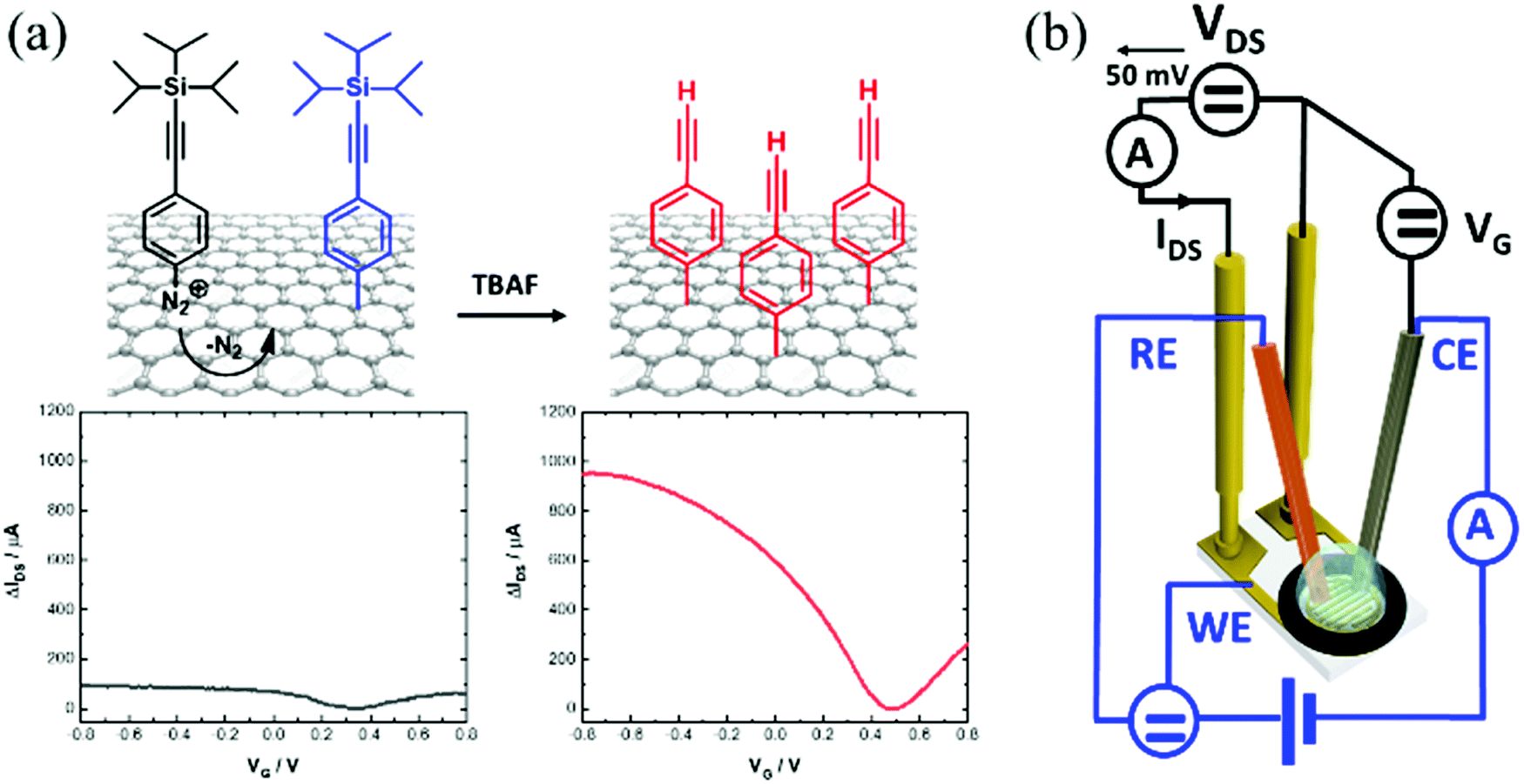 | ||
| Fig. 1 (a) Electrochemically-driven anchoring of 4-[(triisopropylsilyl)ethylenyl]benzene diazonium tetrafluoroborate diazonium salt, followed by chemical deprotection forming alkynyl-terminated GFET devices. IDSVG curve of GFET before (black) and after modification and deprotection (red). (b) Scheme of the liquid gated GFET device allowing for electrical measurements as well as electrochemical surface modifications to be performed. | ||
Even though this surface chemistry approach has been widely employed, the bottleneck to overcome with covalent attachment strategies using diazonium chemistry is to preserve the conductivity of the graphene sheet and its charge mobility. In the case of 4-nitrobenzene diazonium tetrafluoroborate salt, which is by far the most studied aryl diazonium derivative, in most cases,17,23–25 a decrease in graphene conductivity occurs with increasing the grafting time (spontaneous grafting) due to the increased sp2/sp3 transitions. The electron-withdrawing properties of the nitro group lead to a clear positive shift in the Dirac point, resulting in hole doping. Only a few other aryl diazonium salts have been studied for graphene functionalization,26–29 but led to similar observations related to Dirac point shifts and a decrease of conductivity. Very recently, Pagliara and coworkers demonstrated that the electronic structure of graphene can be preserved even after covalent modification by using specifically designed 3,4,5-trimethoxybenzene diazonium salts.13 While this finding is against the possibility to open a band gap in graphene by covalent functionalization and thus the use of graphene in electronic applications, this argues in favor of using graphene as a sensing channel in transistors.
Here we demonstrate that CVD-grown graphene, covalently-modified with a monolayer of phenylacetylene, represents an ideal surface chemistry approach for GFET (Fig. 1a).
Electrochemical reduction of 4-[(triisopropylsilyl)ethynyl]benzene diazonium tetrafluoroborate (TIPS-Eth-ArN2+) and further chemical deprotection of the triisopropylsilyl group results in a graphene modified interface with charge mobility above 1000 cm2 V−1 s−1. This process is not only highly reproducible, but also the anchoring of alkynyl functional groups to the graphene transducer allows for further covalent immobilization of a wide range of molecules in a surface-orientated manner using a Cu(I)-based “click” chemistry reaction.30,31
2. Results and discussion
2.1. Characterization of GFET formed on interdigitated electrodes
In this work, the investigated GFET devices are based on graphene coated interdigitated gold electrodes (IDE) with a layout consisting of 90 pair electrodes, each with a width of 10 μm, separated by 10 μm (Fig. 2a) and arranged in an array of 3.5 mm diameter. The monolayer graphene used in this work is grown by chemical vapor deposition (CVD) on commercial Cu foil. Transfer of graphene onto the IDE was achieved by coating graphene with polymethylmethacrylate (PMMA), a polymer supporting layer, to prevent graphene from collapsing. The wet transfer comprises several steps, (see Scheme S1, ESI†) and uses a slow rate Cu etchant that avoids degradation of graphene. Recording an SEM image of the graphene-coated IDE (Fig. 2a) validates the complete coverage of the drain–source channel with graphene sheets with the quality of a monolayer graphene, as seen from the Raman spectrum (Fig. 2b).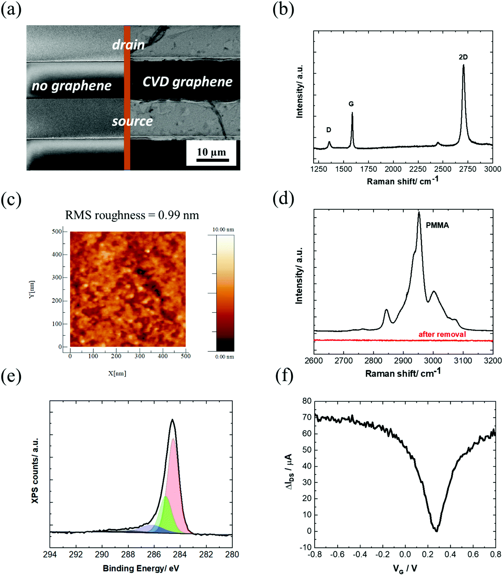 | ||
| Fig. 2 Characterization of the unmodified GFET: (a) SEM image of the IDE chip and after coating with CVD graphene showing full coverage of the drain–source channel. (b) Raman spectrum and (c) AFM image of the graphene channel. (d) Raman spectrum of PMMA coating before and after exposing the graphene/PMMA film to UV/ozone followed by hot acetone washing for 30 min. (e) C 1s core level spectrum of the graphene channel. (f) IDSVG curve of IDE coated with graphene in PBS 1× (equal to IDSVG curve in Fig. 1a, but different scale). | ||
The Raman spectrum of CVD graphene consists of three main peaks at 1350, 1580 and 2706 cm−1 attributed as D (defects in the graphene sheet), G (graphene sp2 carbon) and 2D (secondary D band) peaks, respectively. The low-intensity D + D′′ contribution at ∼2450 cm−1 appears due to a combination between D and the D′′ peak at ∼1100 cm−1 (not shown). The intensity ratio between the 2D and G bands is 2.04. Generally, a 2D/G intensity ratio higher than 2 suggests that the graphene monolayer has low charge impurities and proves the high-quality of the graphene monolayer deposited onto the surface of the device.32 The intensity ratio between the D and G peaks is 0.35 in the graphene lattice after transfer, indicating a low disorder. In order to examine the uniformity of the graphene film, a Raman mapping over 20 × 20 μm2 area was explored. Most of the scanned area has a signature of I2D/IG > 2 and ID/IG< 0.35, which further confirms the uniform coverage of high-quality monolayer graphene (Fig. S1, ESI†).
From the AFM image in Fig. 2c, a surface roughness of about 1 nm is observed, consistent with the deposition of a single graphene layer.33
The low surface roughness is in line with an efficient removal of the PMMA protection layer by first exposing the film to UV/ozone, followed by hot acetone washing for 30 min (Fig. 2d). XPS analysis of the C 1s core level spectrum is dominated by the band at a binding energy BE = 284.7 eV ascribed to the C-sp2. Additional bands at BE = 285.0, 286.4 and 288.6 eV are due respectively to C-sp3 components mostly present at the grain boundaries of the large graphene sheets, and edge functions such as C–O and C![[double bond, length as m-dash]](https://www.rsc.org/images/entities/char_e001.gif) O (Fig. 2e).
O (Fig. 2e).
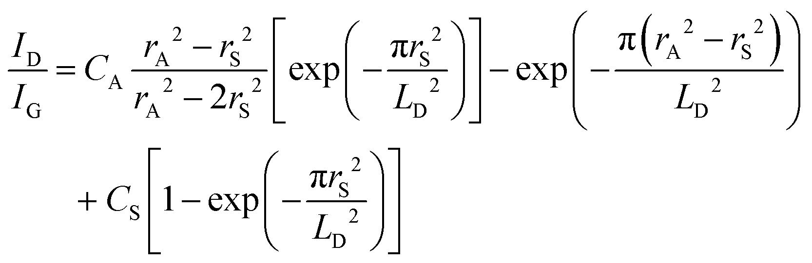
The transfer characteristics of the GFET as a function of the gate voltage (VG) are seen in Fig. 2f. The Dirac point, which corresponds to the charge neutrality point, is found at approximately 0.3 V vs. Ag/AgCl. The field-effect mobility, μef, is obtained from the linear part of the transfer characteristics positive and negative to the Dirac point, using the following equation:
 | (1) |
![[thin space (1/6-em)]](https://www.rsc.org/images/entities/char_2009.gif) 000 cm2 V−1 s−1.34,35 This can be explained by two different phenomena: first, it is now well-known that the choice of the surface onto which graphene is deposited is of utmost importance. For instance, SiO2 surfaces tend to trap charges and impurities which can decrease graphene mobility by at least one order of magnitude.36,37 Here, gold as an IDE on glass has been chosen as a substrate and may impact drastically graphene mobility; second, it is also well-known that a complete removal of the polymer supporting layer (here PMMA) residuals is a problematic issue, even after a long period of exposure to acetone.38 And even if great care has been taken here, such residuals have also a huge impact on the measured graphene mobility. Interestingly, Bouilly and coworkers39 recently reviewed GFETs as bioanalytical sensors. Whereas it is often assumed that high quality and high mobility of the graphene channel on the GFET is a required condition to obtain efficient sensors with low limit of detection (LOD), they observed that there is no significant correlation between graphene quality (mobility) and LOD values. Indeed, from the data collected for this review, reported mobility values as low as 200 cm2 V−1 s−1 for exfoliated graphene40 or 6 cm2 V−1 s−1 for reduced graphene oxide (rGO)41 allowed very low LOD (∼fM or lower) in protein sensors. Hence, the measured graphene mobility above 200 cm2 V−1 s−1 in our case should allow the fabrication of efficient (bio)sensors in a simple way using commercially available IDE substrates without the need for lithography techniques.
000 cm2 V−1 s−1.34,35 This can be explained by two different phenomena: first, it is now well-known that the choice of the surface onto which graphene is deposited is of utmost importance. For instance, SiO2 surfaces tend to trap charges and impurities which can decrease graphene mobility by at least one order of magnitude.36,37 Here, gold as an IDE on glass has been chosen as a substrate and may impact drastically graphene mobility; second, it is also well-known that a complete removal of the polymer supporting layer (here PMMA) residuals is a problematic issue, even after a long period of exposure to acetone.38 And even if great care has been taken here, such residuals have also a huge impact on the measured graphene mobility. Interestingly, Bouilly and coworkers39 recently reviewed GFETs as bioanalytical sensors. Whereas it is often assumed that high quality and high mobility of the graphene channel on the GFET is a required condition to obtain efficient sensors with low limit of detection (LOD), they observed that there is no significant correlation between graphene quality (mobility) and LOD values. Indeed, from the data collected for this review, reported mobility values as low as 200 cm2 V−1 s−1 for exfoliated graphene40 or 6 cm2 V−1 s−1 for reduced graphene oxide (rGO)41 allowed very low LOD (∼fM or lower) in protein sensors. Hence, the measured graphene mobility above 200 cm2 V−1 s−1 in our case should allow the fabrication of efficient (bio)sensors in a simple way using commercially available IDE substrates without the need for lithography techniques.
2.2. Electrochemical surface grafting of TIPS-Eth-ArN2+ on the GFET
Several works reported on efficient graphene functionalization under electrochemical control. It was noted that the application of an electrochemical potential shifts the Fermi level of graphene,17 increasing the probability for a direct attack of the covalent sp2 bonds. We thus opted for the electrochemical grafting of a triisopropylsilyl protected ethynylphenyl diazonium salt (Fig. 1a), 4-[(triisopropylsilyl)ethynyl]benzene diazonium tetrafluoroborate (TIPS-Eth-ArN2+), known for its surface limiting grafting capabilities due to the presence of the bulky triisopropylsilyl (TIPS) group.42,43 For this purpose, cyclic voltammetry was applied as a powerful technique able to monitor in situ electron-transfer processes during the electrochemical reactions. The graphene channel of the GFET was used as the working electrode thanks to the liquid gated configuration of our system (Fig. 1b). A broad monoelectronic cathodic peak is observed at −0.2 V (vs. Ag/AgCl) by scanning the potential from +0.3 V to −0.6 V (vs. Ag/AgCl) at a scan rate of 50 mV s−1 (Fig. 3a). There is no anodic peak associated with the cathodic one, corresponding to the cleavage of N2 groups coupled to the formation of aryl radicals. The electrochemical reduction current of TIPS-Eth-ArN2+ at −0.2 V decreases already after the first cycle, indicating that the graphene channel is blocked by the deposition of an insulating organic film and thus the successful surface functionalization of the latter (Fig. 3a). The success of the surface grafting was additionally validated by XPS analysis (Fig. 3b). The change in the C 1s core level of 4-(triisopropylsilyl)ethynylphenyl (TIPS-Eth-Ar) modified GFET (Fig. 3b) compared to unmodified GFET (Fig. 2e) is in line with a change in the chemical environment after graphene functionalization. Furthermore, after TIPS-Eth-ArN2+ grafting, the presence of the bulky TIPS groups is confirmed by the presence of a Si–C band at 283.7 eV and an increase in the intensity of the C-sp2 component is ascribed to the contribution of the C-sp2 signal from the carbon atoms of the phenyl rings of the diazonium salt. The highly reactive nature of aryl radicals results, in most cases, in the formation of disordered polyaryl layers, which in the case of field effect transistors will reduce the dynamic range of sensing as it might be as thick as the Debye screening length, not being the case while using the bulky TIPS-Eth-ArN2+ precursor which limits the surface modification to a functional monolayer.42,43 Indeed, grafting of a TIPS protected diazonium salt is a self-inhibited process and a full monolayer coverage is reached even after one cycle independent of the concentration of the diazonium salt used (1, 5 and 10 mM). This indicates that ligand density cannot be varied. An increase in surface roughness to 1.87 nm was determined by AFM measurements (Fig. 3c). With a theoretical height of 4-[(triisopropylsilyl)ethynyl]benzene of 1.01 nm,42 the coating thickness is in agreement with a controlled surface grafting of the 4-[(triisopropylsilyl)ethynyl]benzene radical on graphene and the prevention of the formation of multilayer branched structures, as observed in other works.16 The success of the integration of TIPS-Eth-Ar onto graphene in one scan is further evident by the cyclic voltammograms of ferrocenemethanol (1 mM/PBS 1×) on unmodified GFET and GFET modified by TIPS-Eth-Ar (GFET-TIPS) (Fig. 3d). Whereas a reversible oxidation is detected onto unmodified GFET, a complete blocking of the electron transfer from ferrocenemethanol to GFET-TIPS is observed. Comparison of the Raman spectra of transferred CVD graphene before (Fig. 2b) and after electrografting (Fig. 3e) of TIPS-Eth-ArN2+ indicates an increase in the ratio between the D and G band intensity. The D peak arises from the defect-involved double resonant Raman process at the K point in the Brillouin zone44 and is attributed to the transition from sp2 to sp3 hybridization of the graphene carbon atoms. It is an indication of the degree of covalent modification of graphene and as expected the ID/IG ratio increased from 0.35 (GFET) to 0.67 (GFET-TIPS), which demonstrates an increase in the disorder in the graphene lattice due to the covalent modification.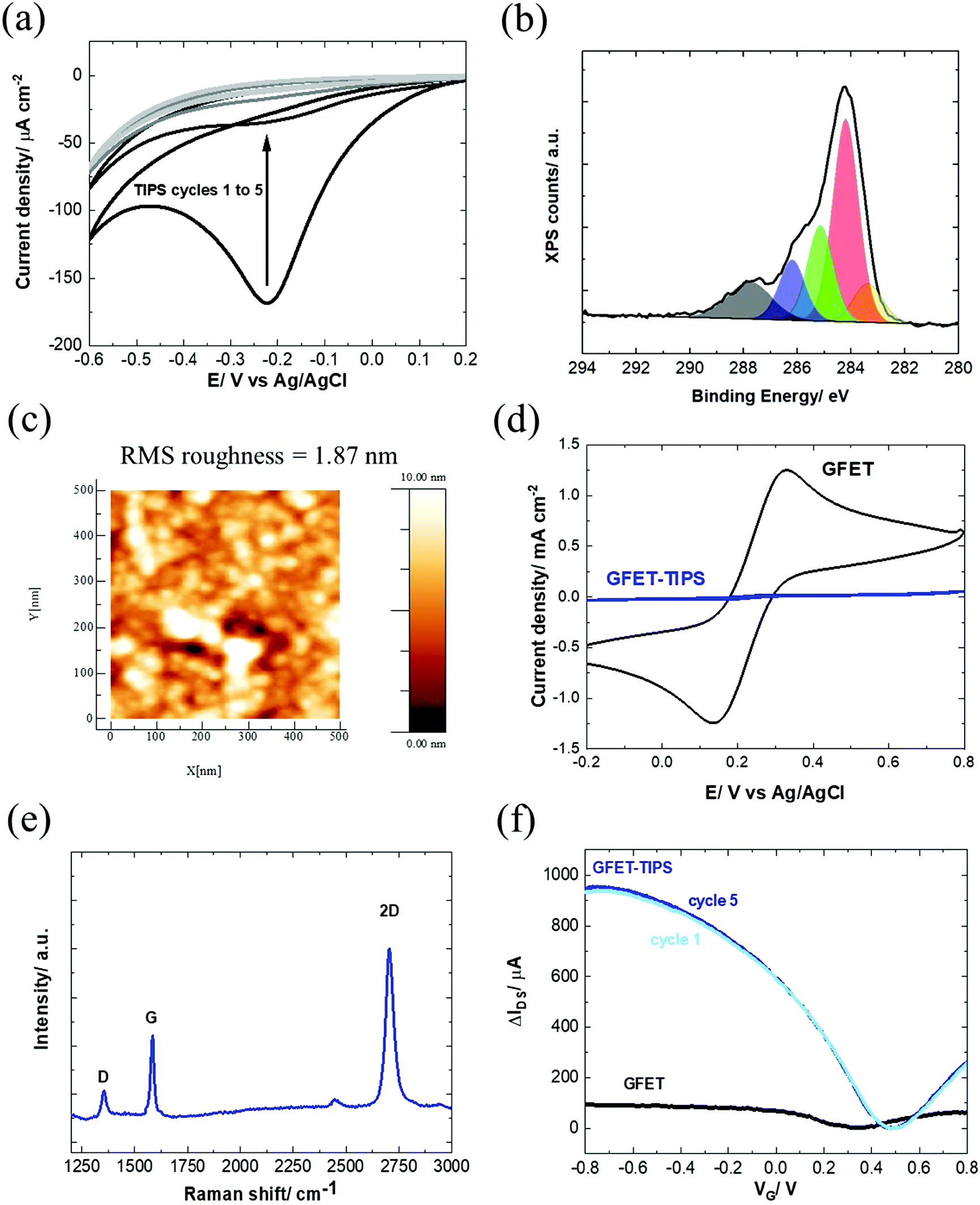 | ||
| Fig. 3 Characterization of the GFET-TIPS: (a) electrochemical reduction of a solution of TIPS-Eth-ArN2+ (10 mM) in 0.1 M n-tetrabutylammonium hexafluorophosphate (nBu4PF6) in acetonitrile via cycling between +0.2 V and −0.6 V (vs. Ag/AgCl) at a scan rate of 50 mV s−1. The reduction peak is visible at approximately −0.2 V vs. Ag/AgCl. (b) C 1s core level spectrum and (c) AFM image of the GFET-TIPS channel. (d) Cyclic voltammograms of ferrocenemethanol (1 mM/PBS 1×) on GFET and GFET-TIPS; scan rate=100 mV s−1. (e) Raman spectrum of GFET-TIPS. (f) Transfer characteristics of GFET before (black) and after modification with TIPS-Eth-ArN2+ (blue) for several cycles. The IDSVG of GFET before (black) is the same as that illustrated in Fig. 1(a) and integrated to allow easier comparison. | ||
Interestingly, electrografting of aryl diazonium salts results in strongly improved IDSVG curve characteristics (Fig. 3f) with slopes as steep as ∼1750 μA V−1. The process proved in addition to be highly reproducible (Fig. S3b, ESI†) with hole mobility, μh, and electron mobility, μe, of 1739 ± 376 cm2 V−1 s−1 and 1698 ± 536 cm2 V−1 s−1, respectively as determined on 10 different devices. Furthermore, the stability of the TIPS modified GFET devices evaluated 1 month after having been stored in the dark at room temperature is remarkably maintained, being observed just a slight decay on the drain–source current, but a negligible shift of the Dirac point (Fig. S3b, ESI†). As such, graphene p-doping produced by the grafting of TIPS-protected diazonium does not change overtime.
This observation is contradictory with a covalent functionalization implying an increase of the number of carbon atom hybridizations from sp2 to sp3 leading to a decrease of graphene charge mobility. Ago et al.45 already reported that short exposures to aryl diazonium can have a positive effect by removing polymer residuals present on the surface of graphene samples which can explain in our case the improved conductivity of the GFET-TIPS channel. These values of charge mobilities have to be compared with the one found in the literature. In the majority of the examples, covalent functionalization of graphene has been performed using spontaneous grafting. As mentioned above, using spontaneous grafting, covalent functionalization is favored on the edges and defects of graphene materials19–22 and leads to lower surface coverage than electrochemically induced aryl diazonium grafting. Whereas spontaneous grafting often leads to graphene charge mobility below 600 cm2 V−1 s−1,23,29,46,47 when considering electrochemically-driven aryl diazonium reduction this value decreases down to 10 cm2 V−1 s−1.17 Such mobility value above 1000 cm2 V−1 s−1 is unprecedented and can be explained by the controlled surface functionalization of the graphene channel by using specifically designed sterically hindered aryl diazonium salts, allowing the covalent attachment of only a monolayer.
Modification of the electronic properties of the graphene channel is achieved during the first cycle. The following cycles do not alter the overall behavior. The Dirac point shifted from +0.3 V (vs. Ag/AgCl) to +0.5 V (vs. Ag/AgCl) for GFET-TIPS. In control experiments, GFETs were cycled between +0.2 V and −0.6 V (vs. Ag/AgCl) in an acetonitrile solution containing only 0.1 M n-tetrabutylammonium hexafluorophosphate salt (nBu4PF6) as a supporting electrolyte, in the absence of diazonium salt. The transfer characteristic remained the same, ruling out any electrochemical doping (Fig. 4a).
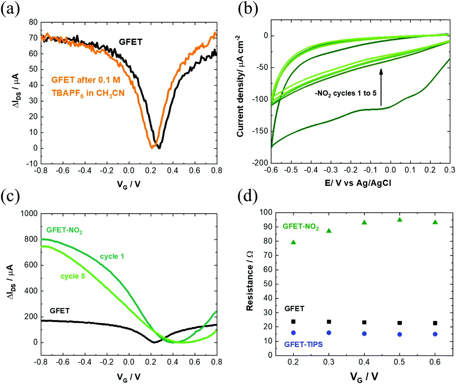 | ||
| Fig. 4 Control experiments: (a) IDSVG of GFET before (black) and after (orange) electrochemical cycling at a scan rate of 50 mV s−1 in 0.1 M n-tetrabutylammonium hexafluorophosphate (nBu4PF6) in acetonitrile. (b) Electrochemical reduction of a solution of 4-nitrobenzene diazonium tetrafluoroborate (10 mM) in 0.1 M nBu4PF6 in acetonitrile via cycling between +0.3 V and −0.6 V (vs. Ag/AgCl) at a scan rate of 50 mV s−1. The reduction peak is visible at approximately −0.05 V vs. Ag/AgCl. (c) IDSVG of GFET-NO2 after 1 and 5 cycles as compared to pristine GFET. (d) Variation of resistivity with applied VG for GFET (black), GFET-TIPS (blue) and GFET-NO2 (green). | ||
The change of the Dirac point to more positive values is in line with the p-doping effect of the latter one. This has been also observed by others for GFETs functionalized with 4-nitrobenzene diazonium salt.23,48 To understand the mechanism behind the transfer characteristics, a scatter plot of the peak position of the 2D band (ω2D) vs. the position of the G Raman band (ωG) was constructed by extracting the parameters from Raman mapping experiments of a GFET-TIPS interface (Fig. S4, ESI†). To distinguish between n- and p-doping, the trend from literature data of mechanically exfoliated monolayer graphene doped by electrostatic gating is included.49 The initial GFET device lies in the very low doped region, while after functionalization, graphene is shifted along the p-doped branch. The density of the reacted sites σ, quantitatively correlated with ID/IG ratios, was extracted using the correlation defined by Lucchese et al.:50
 | (2) |
We performed the same experiment with 4-nitrobenzene diazonium tetrafluoroborate (Fig. 4b) as well with some other diazonium salts (Fig. S5, ESI†). In all cases, the same phenomenon was observed as with TIPS-Eth-ArN2+: an increase in mobility after the first cycle, decreasing however with consecutive scans due to the formation of multilayered branched structures (Fig. 4c). The final charge mobilities of the different GFET modified interfaces (Table S1, ESI†) were all less compared to that recorded on the GFET modified with TIPS-Eth-ArN2+ diazonium salt. Finally, GFET-TIPS channels have a decreased resistivity compared to GFET alone, which is almost independent of gate voltage applied (Fig. 4d). Such behavior has also been observed by Gao et al. considering graphene covalently functionalized by 4-nitrobenzene diazonium salts.46 Table S1 (ESI†) lists the graphene mobility values related to the other aryl diazonium salts we used for comparison and are in line with our findings.
2.3. TIPS deprotection and click chemistry
In order to have access to the alkynyl groups, a deprotection step is mandatory. Stable and highly reproducible ethynyl-terminated graphene channels were formed via the electro-chemical reduction of TIPS-Eth-ArN2+ followed by chemical deprotection of the TIPS group with tetrabutylammonium fluoride (TBAF) solution (Fig. 5a). Chemical deprotection of the TIPS group with TBAF does not alter the transfer characteristics of the GFET as a function of gate voltage, VG (Fig. 5b). The Dirac point (Fig. 5b) shifted from +0.5 V back to +0.3 V after removal of the TIPS groups. Indeed, the formed ethynyl-terminated graphene channels with no particular electron donating or withdrawing group did not cause any obvious change in either the n- or p-type doping of the graphene. The presence of fluoride ions also did not modify the conductivity level of graphene. This is in line with the Raman image of ethynyl-terminated chips (Fig. 5c), with comparable ID/IG ratio as for GFET-TIPS (Fig. 3e), confirming that the chemical treatment of the surface with TBAF only removed the TIPS groups without affecting the graphene lattice. Lucchese et al.50 reported an adapted simple formula allowing a rough estimation of the distance between attached aryl groups, La, from the ID/IG ratio, where (1/La)2 ∼ ID/IG. From this formula, after electrografting, we estimated La to be ∼ 1.5 nm corresponding to a surface coverage Γ ∼ 10−10 mol cm−2. The deprotected substrate was further treated by “click” chemistry reaction (Huisgen 1,3-dipolar cycloaddition30,31) using azidomethylferrocene (Fig. 5a). The success of the incorporation of ferrocene units onto the GFET is seen from the presence of the Fe 2p component in the XPS survey spectrum (Fig. 5d).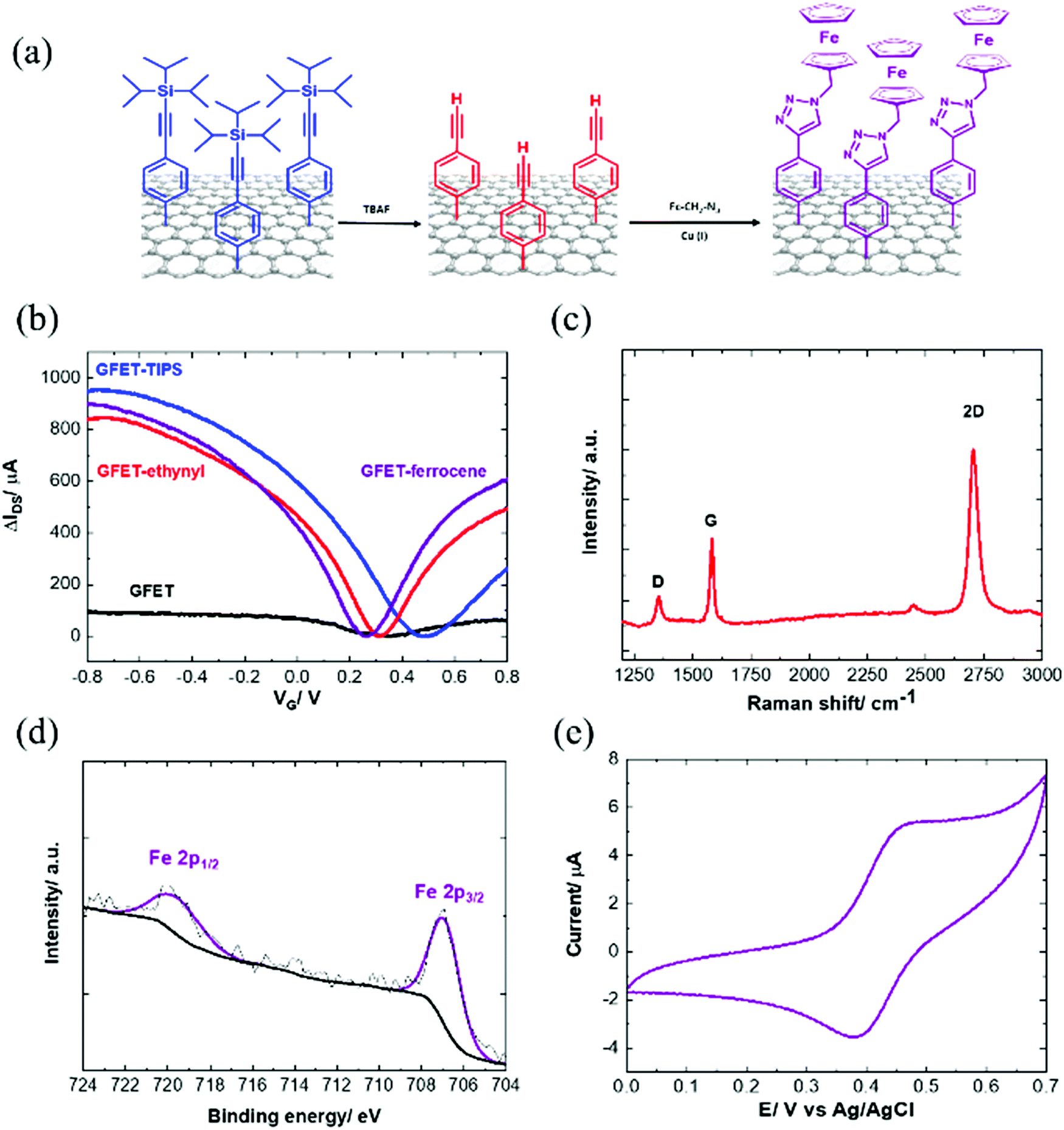 | ||
| Fig. 5 (a) Formation of ethynyl-terminated GFET via deprotection of GFET-TIPS followed by integration of azide-terminated ferrocene through the Cu(I) “click” chemistry approach. (b) IDSVG of GFET-ethynyl and GFET-ferrocene. (c) Raman spectrum of GFET-ethynyl. (d) High resolution Fe 2p XPS core level spectrum of ferrocene-modified GFET interfaces. (e) Cyclic voltammogram of GFET-ferrocene in ethanol/LiClO4 (0.1 M), scan rate = 100 mV s−1. | ||
Fig. 5e depicts the cyclic voltammogram of the ferrocene-modified electrode examined in an electrolytic ethanol solution. A surface concentration of Γ = 3.8 × 10⁻¹⁰ mol cm−2 of bound ferrocene groups was derived from these measurements using the following equation:
| Γ = Q/nFA | (3) |
The positive shift of Dirac point is believed to be in correlation with p-doping due to the presence of the electron withdrawing nature of the ferrocenyl group or the triazole linkage after the click chemistry.
To validate the general concept of the interest of ethynyl modified GFETs, different azide-terminated ligands, such as N3-terminated poly(ethylene glycol) (PEG) (N3-PEG-NH2, N3-PEG-COOH and N3-PEG-Iodoacetyl) as well as azide-terminated bioreceptors, in our case a tetrahydrocannabinol aptamer (N3-aptamer), were clicked onto the ethynyl-terminated GFET and the electronic transfer characteristics were determined (Fig. S6, ESI†). The charge mobility of graphene modified with the click interfaces ranges from 839 to 1110 cm2 V−1 s−1 for holes and 840 to 1056 cm2 V−1 s−1 for electrons, respectively (Table S2, ESI†). It is therefore demonstrated that the charge transfer characteristics of the modified GFET remain similar even after the covalent attachment of complex biological molecules via a click chemistry coupling reaction.
3. Conclusion
In summary, we covalently functionalized the graphene channel of a graphene-base field effect transistor (GFET) with an ethynylphenyl monolayer in a controlled manner, via the electroreduction of a specifically designed 4-[(triisopropylsilyl)ethynyl]benzene diazonium salt (TIPS-Eth-ArN2+). The graphene functionalization requires only one voltammetry cycle to achieve a self-inhibited monolayer coverage. Considering the huge impact of such covalent functionalization on the graphene lattice, the GFET keeps a high charge mobility above 1000 cm2 V−1 s−1. It largely outperforms GFETs modified with other aryl diazonium salts, such as the well-known 4-nitrobenzene diazonium tetrafluoroborate. The functionalization process furthermore induced p-type doping due to the electron-withdrawing properties of the triisopropylsilyl (TIPS) protecting groups. Whereas after TIPS deprotection such p-type doping is no longer observed, and the GFET charge mobility is preserved. Raman spectroscopy data are in line with the finding that the integration of TIPS-Eth-Ar introduces only small defects. The introduction of a wide range of (bio) molecules by a “click” chemistry reaction (Huisgen 1,3-dipolar cycloaddition) is therefore possible and evidenced here by the immobilization of a monolayer of redox active ferrocenyl moieties. It is also important to note here that the fabrication process of the GFET only involved graphene transfer onto commercially available gold interdigitated electrode (IDE) substrates without the need of any lithography techniques. Such a device is ideally suited for achieving highly sensitive GFET based sensing devices, with a symmetric IDSVG curve and slopes of ∼1750 μA VG−1. We are currently investigating the sensitivity and LOD of such devices as a biosensor for sensing of cardiac troponin I. Indeed, cardiovascular diseases result in millions of deaths around the globe, many of which could have been avoided if identified at an early stage. The specific sensing of cTnI on TIPS-modified GFET diagnostics might be a step in this direction, but needs still further considerations, notable clinically relevant sample analysis, out of the scope of this work.4. Experimental section
Chemicals
Tetrabutylammonium fluoride (TBAF), 4-bromobenzenediazonium tetrafluoroborate (96%), 4-nitrobenzenediazonium tetrafluoroborate, copper(I) sulfate (CuSO4), L-ascorbic acid, ethylenediaminetetraacetic acid (EDTA), N-butylhexafluorophosphate (nBu4PF6) and O-(2-aminoethyl)-O′-(2-azidoethyl)heptaethylene glycol (N3-PEG-NH2), were purchased from Sigma-Aldrich and used as-received. 4-((Triisopropylsilyl)ethylenyl)benzene diazonium tetrafluoroborate (TIPS-Eth-ArN2+) and azidomethylferrocene were synthesized as reported previously.43Azido-PEG-acid was purchased from Broadpharm (San Diego, USA) and iodoacetyl-PEG-azide was purchased from NanoCS (New York, USA).
5′-Azide modified tetrahydrocannabinol aptamer (5′-NH2-TTT-TTT-CTT ACG ACC CAG GGG GGT GGA CAG GCG GGG GTT AGG GGG GTC GTA AG-3′) was purchased from integrated DNA Technologies (Leuven, Belgium).
Materials
Prior to graphene transfer, the interdigitated microelectrodes (ED-IDE1-Au w/o SU8, Micrux Technologies) are cleaned in a UV-Ozone chamber (Jelight, USA) for 10 min followed by submersion for 15 min sequentially in 10 mL of acetone, isopropanol and water. Finally, every chip is copiously rinsed with a large amount of water and dried under a nitrogen flow. The cleaned interfaces are placed in a plastic Petri dish and stored in a desiccator under vacuum. The cleaned IDE are modified with trimethoxyphenylsilane (TMPS, 300 μL of TMPS in 15 mL of ethanol) in a plastic falcon tube for 1 h. Afterwards, the electrodes are immersed for 15 min in ethanol to remove the excess of the silane compounds from the surface. Subsequently, the modified interfaces are nitrogen blow dried and stored under vacuum. The chips are placed on a hot plate at 120 °C at ambient pressure for 2 h to anneal the formed monolayer and provide complete removal of the solvents from the surface. Graphene is directly transferred to these interfaces.Graphene
The monolayer graphene is grown by chemical vapor deposition (CVD) on commercial Cu foil from Alpha Aesar (high purity – 99.9999%). Graphene growth is carried out in a Jipelec JetFirst Rapid Thermal CVD (RTCVD). This system allows heating and cooling at high rates (10 °C s−1). The growth itself comprises heating, annealing, growth and cooling steps. We used a mixture of 100 sccm of argon and 5 sccm of dihydrogen during all the steps and 20 sccm of methane as a precursor during the growth phase. We first cut the Cu foil into small pieces (2.5 × 2.5 cm), and cleaned them with acetic acid, acetone and IPA for 5 min each under ultrasonication in order to remove all possible copper oxide and to produce the cleanest surface possible. We then put the pieces onto a Si wafer in the chamber. We proceed to a high vacuum (<5 × 10⁻⁵ bar) before starting and then the sample is heated for 5 min from room temperature to 300 °C, followed by 2 min from 300 °C to 1070 °C, annealing for 5 min, growth for 5 min and finally, a quick cooling of the chamber using a water flow (with a decrease rate of 60 °C s−1 from 1000 to 700 °C), for 10 min to reach room temperature.Transfer
A polymethyl methacrylate (PMMA) film of 200 nm in thickness is spin-coated onto the graphene/Cu foil and annealed at 110 °C with a very slow heating and cooling rate (1 °C min−1) in order to prevent cracks in the graphene due to the difference of the thermal expansion coefficient between copper and graphene. The graphene on the back side of the Cu foil was removed by reactive ion etching (RIE) in an O2 plasma (50 W/100 mT/25 sccm/1 min). Copper foil etching was achieved in 0.2 M ammonium persulfate ((NH4)2S2O8) for 8 h and the floating PMMA/graphene sample was put in DI water. This operation was repeated about 10 times in order to rinse the graphene from the etchant solution. Graphene transfer onto the IDE was achieved by submerging the IDE under the floating graphene/PMMA film. To remove traces of trapped water between graphene and IDE and to increase the adhesion of graphene to the IDE, the substrate was placed on a hot plate and annealed at 90 °C for 30 min using a slow heating and cooling rate (1 °C min−1). The PMMA layer was effectively removed by UV/ozone cleaning at 28–35 mW cm−2 for 5 min followed by a hot acetone rinse (30 °C for 30 min).Electrografting
The electrografting of 4-((triisopropylsilyl)ethylenyl)benzene diazonium tetrafluoroborate (TIPS-Eth-ArN2+) (10 mM) in 0.1 M n-tetrabutylhexafluorophosphate (nBu4PF6) in acetonitrile was performed using cyclic voltammetry at a scan rate of 50 mV s−1 for five cycles between +0.20 V and −0.60 V vs. Ag/AgCl. The electrodes were rinsed with copious amounts of acetonitrile and acetone and gently dried under an argon atmosphere.TIPS deprotection
A TIPS protecting group was removed by the immersion of the interface into tetrabutylammonium fluoride (TBAF, 0.1 M in THF) for 1 h at room temperature. The surface was then left for 15 min in a pure THF solution for cleaning. This modification process produces an ethynyl-terminated GFET.Cu(I)-catalyzed click chemistry
Ethynyl-terminated GFET was immersed into an aqueous solution of CuSO4 (10 mM) and L-ascorbic acid (20 mM) in the presence of azidomethylferrocene (0.83 mM in THF) and left for 1 h under an argon atmosphere. The interface was then treated with an aqueous solution of EDTA for 10 min to chelate any remaining Cu2+ residues and finally washed copiously with acetone and water and left for ambient drying.Instrumentation
X-ray photoelectron spectroscopy (XPS) was performed on a PHI 5000 VersaProbe-Scanning ESCA Microprobe (ULVAC-PHI, Japan/USA) instrument at a base pressure below 5 × 10⁻⁹ mbar. Core level spectra were acquired at a pass energy of 23.5 eV with a 0.1 eV energy step. All spectra were acquired with 90° between X-ray source and analyzer and with the use of low energy electrons and low energy argon ions for charge neutralization. After subtraction of the linear background, the core-level spectra were decomposed into their components with mixed Gaussian–Lorentzian (30:70) shape lines using the CasaXPS software.
Quantification calculations were conducted using sensitivity factors supplied by PHI. Scanning electron microscopy (SEM) images were obtained using an ULTRA 55 electron microscope (Zeiss, France) equipped with a thermal field emission emitter and three different detectors (EsB detector with filter grid, high efficiency In-lens SE detector and Everhart–Thornley Secondary Electron Detector). Raman spectroscopy measurements were performed on a LabRam HR Micro-Raman system (Horiba Jobin Yvon, France) combined with a 473 nm laser diode as the excitation source. Visible light was focused by a 100× objective. The scattered light was collected by the same objective in backscattering configuration, dispersed by a 1800 mm focal length monochromator and detected by a CCD. Raman images in mapping conditions were obtained from a 10 × 10 point array with 2 μm spacing between two consecutive points. Each data point was acquired during 5 s exposure time and is the average over three measurements. The background caused by the gold scattering was corrected against a blank measurement of the clean gold electrode. The images were generated using LabSpec software. Tapping mode AFM images in air and ambient temperature were recorded using a Bruker, Dimension 3100 AFM. The surfaces were imaged with a silicon cantilever (AppNano TM300, typical spring constant: 50 N m−1) working at a frequency of 369 kHz. Image treatment and RMS (root-mean square) roughness Ra were obtained with the WSXM software. Surface roughness of the samples was measured by scanning over a 5 × 5 μm area. Cyclic voltammograms were acquired on a potentiostat/galvanostat (Metrohm Autolab, The Netherlands). Electrical measurements were conducted using a probe station source meter unit U2322A (Keysight Technologies, USA). All measurements were performed using a PMMA commercial flow cell (Micrux Technologies, Spain) with fixed flow channel geometry (16 μL), ensuring a defined flow rate of 50 μL min−1 to minimize mass transport limitations of the analyte to the sensor surface in all experiments. A silver chloride wire (diameter 1 mm, Sigma-Aldrich) was used to operate the GFET device in liquid gate configuration, with a constant source–drain bias (VDS) of 0.05 V, sweeping the gate voltage (VG) between −0.8 V and 0.8 V.
Conflicts of interest
There are no conflicts to declare.Acknowledgements
Financial support from the Centre National de la Recherche Scientifique (CNRS) and the University of Lille is acknowledged.References
- F. Schwierz, Nat. Nanotechnol., 2010, 5, 487–496 CrossRef CAS PubMed.
- Y. Shao, J. Wang, H. Wu, J. Liu, I. A. Aksay and Y. Lin, Electrocalaysis, 2010, 22, 1027–1036 CrossRef CAS.
- V. Georgakilas, J. N. Toiwari, C. Kemp, J. A. Perman, A. B. Boulinos, K. S. Kim and R. Zboril, Chem. Rev., 2016, 9, 5464–5519 CrossRef PubMed.
- J. Park and M. Yan, Acc. Chem. Res., 2013, 46, 181 CrossRef CAS PubMed.
- C. K. Chua and M. Pumera, Chem. Soc. Rev., 2013, 43, 3222 RSC.
- K. S. Novoselov, A. K. Geim, S. V. Morozov, D. Jiang, Y. Zhang, S. V. Dubonos, I. V. Grigorieva and A. A. Firsov, Science, 2004, 306, 66 CrossRef PubMed.
- F. Schedin, A. K. Geim, S. V. Morozov, E. W. Hill, P. Blake, M. I. Katsnelson and K. S. Novoselov, Nat. Mater., 2007, 6, 652–655 CrossRef CAS PubMed.
- J. Lee, E. Hwang, E. Lee, S. Seo and H. Lee, Chem. – Eur. J., 2012, 18, 5155–5159 CrossRef CAS.
- W. Fu, L. Jiang, E. P. van Geest, L. M. C. Lima and G. F. Schneider, Adv. Mater., 2017, 29, 1603610 CrossRef PubMed.
- J. Liu, J. Tang and J. J. Gooding, J. Mater. Chem., 2012, 22, 12435–12452 RSC.
- A. Lopez and J. Liu, Adv. Intell. Syst., 2020, 2, 2000123 CrossRef.
- G. L. C. Paulus, Q. H. Wang and M. S. Strano, Acc. Chem. Res., 2012, 46, 160–170 CrossRef PubMed.
- G. Ambrosio, A. Brown, L. Daukiya, G. Drera, G. Di Santo, L. Petaccia, S. De Feyter, L. Sangaletti and S. Pagliara, Nanoscale, 2020, 12, 9032–9037 RSC.
- D. K. H. Tsang, T. J. Lieberthal, C. Watts, I. E. Dunlop, S. Ramadan, A. E. del Rio Hernandez and N. Klein, Sci. Rep., 2019, 9, 13946 CrossRef PubMed.
- E. Beyarova, M. E. Itkis, P. Ramseh, C. Berger, M. Spinkle, W. A. de Heer and R. C. Haddon, J. Am. Chem. Soc., 2009, 131, 1336–1337 CrossRef PubMed.
- Z. Xia, F. Leonardi, M. Gobbi, Y. Liu, V. Bellani, A. Liscio, A. Kovtun, R. Li, X. Feng, E. Origu, P. Samori, E. Treossi and V. Palermo, ACS Nano, 2016, 10, 7125–7134 CrossRef CAS PubMed.
- C.-J. Shi, Q. H. Wan, Z. Jin, G. L. C. Paulus, D. Blankschtein, P. Jarillo-Herrero and M. S. Strano, Nano Lett., 2013, 13, 809–817 CrossRef.
- D.-e. Jiang, B. G. Sumpter and S. Dai, J. Phys. Chem. B, 2006, 110, 23628 CrossRef CAS PubMed.
- H. Lim, J. S. Lee, H.-J. Shin, H. S. Shin and H. C. Choi, Langmuir, 2010, 26, 12278–12284 CrossRef CAS PubMed.
- Z. Sun, S.-i. Kohama, Z. Zhang, J. R. Lomeda and J. M. Your, Nano Res., 2013, 3, 117–125 CrossRef.
- F. M. Koheler, A. Jacobus, K. Ensslin, C. Stampfer and W. J. Stark, Small, 2010, 6, 1125–1130 CrossRef PubMed.
- R. Sharma, J. H. BAik, C. J. Perera and M. S. Strano, Nano Lett., 2010, 10, 398–405 CrossRef CAS PubMed.
- X.-Y. Fan, R. Nouchi, L.-C. Yin and K. Tanigaki, Nanotechnology, 2010, 21, 475208 CrossRef PubMed.
- E. Pembroke, G. Ruan, A. Stinitskii, D. A. Corley, Z. Yan, Z. Sun and J. M. Your, Nano Res., 2013, 6, 138–148 CrossRef CAS.
- D. Bousa, O. Jankovsky, D. Semidubsky, J. Luxa, J. Strural, M. Pumera and Z. Sofer, Chem. – Eur. J., 2015, 21, 17728–17738 CrossRef CAS PubMed.
- D. B. Farmer, R. Goliazadeh-Mojarad, V. Perebeinos, Y.-M. Lin, G. S. Tulevski, J. C. Tsand and P. Avouris, Nano Lett., 2009, 9, 388–392 CrossRef CAS PubMed.
- X. Dong, Q. Long, A. Wei, W. Zhang, L.-J. Li, P. Chen and W. Huang, Carbon, 2012, 1517–1522 CrossRef CAS.
- M. Min, S. Seo, J. Lee, S. M. Lee, E. Hwang and H. Lee, Chem. Commun., 2013, 49, 6289 RSC.
- J. Lu, A. Lipatov, N. S. Vorebeva, D. S. Muratov and A. Sinitskii, Adv. Electron. Mater., 2018, 4, 1800021 CrossRef.
- V. V. Rostovtsev, L. G. Green, V. V. Fokin and K. B. Sharpless, Angew. Chem., Int. Ed., 2002, 41, 2596 CrossRef CAS PubMed.
- C. W. Tornoe, C. Christensen and M. Meldal, J. Org. Chem., 2002, 67, 3057 CrossRef CAS PubMed.
- J.-B. Wu, M.-L. Lin, X. Cong, H.-N. Liu and P.-H. Tan, Chem. Soc. Rev., 2018, 47, 1822–1873 RSC.
- L. Zhou, L. Fox, M. Wlodek, L. Islas, A. Slastanova, E. Robles, O. Bikondoa, R. Harniman, N. Fox, M. Cattelan and W. H. Briscoe, Carbon, 2018, 136, 255–261 CrossRef CAS.
- K. I. Bolotin, K. J. Sikes, Z. Jiang, M. Klima, G. Fudenberg, J. Hone, P. Kim and H. L. Stormer, Solid State Commun., 2008, 146, 351–355 CrossRef CAS.
- S. V. Morozov, K. S. Novoselov, M. I. Katsnelson, F. Schedin, D. C. Elias, J. A. Jaszczak and A. K. Geim, Phys. Rev. Lett., 2008, 100, 016602 CrossRef CAS PubMed.
- W. Fu, L. Jiang, E. P. van Geest, L. M. C. Lima and G. F. Schneider, Adv. Mater., 2017, 29, 1603610 CrossRef.
- J.-H. Chen, C. Jang, S. Xiao, M. Ishigami and M. S. Fuhrer, Nat. Nanotechnol., 2008, 3, 206–209 CrossRef CAS.
- J. W. Suk, W. H. Lee, J. Lee, H. Chou, R. D. Piner, Y. Hao, D. Akinwande and R. S. Ruoff, Nano Lett., 2013, 13, 1462–1467 CrossRef CAS PubMed.
- A. Béraud, M. Sauvage, C. M. Bazán, M. Tie, A. Bencherif and D. Bouilly, Analyst, 2021, 146, 403–428 RSC.
- T. Ono, Y. Kanai, K. Inoue, Y. Watanabe, S.-i. Nakakita, T. Kawahara, Y. Suzuki and K. Matsumoto, Nano Lett., 2019, 19, 4004–4009 CrossRef CAS PubMed.
- M. Hasegawa, Y. Hirayama, Y. Ohno, K. Maehashi and K. Matsumoto, Jpn. J. Appl. Phys., 2014, 53, 05FD05 CrossRef CAS.
- Y. R. Leroux and P. Hapiot, Chem. Mater., 2013, 25, 489–495 CrossRef CAS.
- Y. R. Leroux, F. Hui, J.-M. Noel, C. Roux and P. Hapiot, J. Am. Chem. Soc., 2010, 132, 14039–14041 CrossRef CAS PubMed.
- S. Reich and C. Thomsen, Philos. Trans. R. Soc., A, 2004, 362, 2271–2288 CrossRef CAS PubMed.
- P. Solís-Fernández, M. A. Bissett, M. Tsuji and H. Ago, Nanoscale, 2015, 7, 3572–3580 RSC.
- P. Huang, H. Zhu, L. Jiang, Y. Zhao and X. Gao, ACS Nano, 2011, 5, 7945–7949 CrossRef CAS.
- E. Pembroke, G. Ruan, A. Sinitskii, D. A. Corley, Z. Yan, Z. Sun and J. M. Tour, Nano Res., 2013, 6, 138–148 CrossRef CAS.
- Q. H. Wang, Z. Jin, K. K. Kim, A. J. Hilmer, G. L. C. Paulus, C.-H. Shih, M.-H. Ham, J. D. Sanchez-Yamagishi, K. Watanabe, T. Taniguchi, J. Kong, P. Jarillo-Herrero and M. S. Strano, Nat. Chem., 2012, 4, 724 CrossRef CAS PubMed.
- A. Das, S. Pisana, B. Chakraborty, S. Piscanec, S. K. Saha, U. V. Waghmare, K. S. Novoselov, H. R. Krishnamurhty, A. K. Geim, A. C. Ferrari and A. K. Sood, Nat. Nanotechnol., 2008, 3, 210–215 CrossRef CAS.
- M. M. Lucchese, F. Stavale, E. H. Martins Ferreira, C. Vilani, M. V. O. Moutinho, R. B. Capaz, C. A. Achete and A. Jorio, Carbon, 2010, 48, 1592–1597 CrossRef CAS.
- C. E. D. Chidsey, C. R. Bertozzi, T. M. Putvinski and A. M. Mujsce, J. Am. Chem. Soc., 1990, 112, 4301–4306 CrossRef CAS.
Footnote |
| † Electronic supplementary information (ESI) available. See DOI: 10.1039/d1nh00355k |
| This journal is © The Royal Society of Chemistry 2021 |