
Unambiguous determination of crystal orientation in black phosphorus by angle-resolved polarized Raman spectroscopy†
Bo
Zou‡
a,
Yadong
Wei‡
 b,
Yan
Zhou
c,
Dingning
Ke
d,
Xu
Zhang
a,
Meng
Zhang
a,
Cho-Tung
Yip
a,
Xiaobin
Chen
a,
Weiqi
Li
*b and
Huarui
Sun
*a
b,
Yan
Zhou
c,
Dingning
Ke
d,
Xu
Zhang
a,
Meng
Zhang
a,
Cho-Tung
Yip
a,
Xiaobin
Chen
a,
Weiqi
Li
*b and
Huarui
Sun
*a
aSchool of Science and Ministry of Industry and Information Technology Key Laboratory of Micro-Nano Optoelectronic Information System, Harbin Institute of Technology, Shenzhen, 518055, China. E-mail: huarui.sun@hit.edu.cn
bSchool of Physics, Harbin Institute of Technology, Harbin, 150001, China. E-mail: tccliweiqi@hit.edu.cn
cCenter for High Pressure Science & Technology Advanced Research, Shanghai 201203, China
dExperiment and Innovation Center, Harbin Institute of Technology Shenzhen Graduate School, Shenzhen, 518055, China
First published on 24th July 2021
Abstract
Angle-resolved polarized Raman spectroscopy (ARPRS) is widely used to determine the crystal orientations of anisotropic layered materials (ALMs), which is an essential step to study all of their anisotropic properties. However, the understanding of the ARPRS response of black phosphorous (BP) as a most widely studied ALM is still unsatisfactory. Here, we clarify two key controversies about the physical origin of the intricate ARPRS response and the determination of crystal orientations in BP. Through systematic ARPRS measurements, we show that the degree of anisotropy of the response evolves gradually and periodically with the BP thickness, eventually leading to the intricate response. Meanwhile, we find that using the Raman peak intensity ratio of the two Ag phonon modes, the crystal orientations of BP can be unambiguously distinguished via a concise inequality  . Comprehensive analysis and first-principles calculations reveal that the external anisotropic interference effect and the intrinsic electron–phonon coupling are responsible for the observations.
New conceptsThe determination of crystal orientation is crucial for anisotropic layered materials as all chirality-relevant studies and device applications require correlating the crystal orientation with the corresponding anisotropic properties. Angle-resolved polarized Raman spectroscopy is widely used to determine the crystal orientation of anisotropic layered materials; however, there were still two key controversies that urgently needed to be resolved in related research on black phosphorus (BP). In this work, these disputes have been solved. We directly reveal the role of external interference effect and internal electron–phonon coupling in modulating the intricate polarized Raman response of BP by extensive experiments. Also, we show that by constructing the Raman peak intensity ratio, the external optical effect can be eliminated and the AC and ZZ directions of BP can be unambiguously determined by the phonon-mode dependent electron–phonon coupling, which is also supported by density functional theory calculations. The integrated generic method we have proposed, including experimental measurements and theoretical calculations, paves the way for fully understanding and even predicting the polarized Raman response of other anisotropic layered materials, and can also further facilitate fundamental studies and device applications based on these materials. |
Introduction
Anisotropic layered materials (ALMs), such as orthorhombic black phosphorus (BP),1–3 monoclinic gallium telluride (GaTe),4 and triclinic rhenium disulfide (ReS2),5 can provide additional degrees of freedom in tuning physical properties due to the in-plane structural anisotropy.6–13 Among these ALMs, BP has aroused particular interest in recent years owing to its ultra-high room temperature carrier mobility6–9 and adjustable direct bandgap of various thicknesses,13–16 which bridges the energy gap between graphene and transition metal dichalcogenides.17 Either for the fundamental understanding of chirality-relevant studies on BP or for the practical application of BP-based devices, it is crucial to develop a reliable experimental method to conveniently and accurately correlate BP's crystal orientations (zigzag (ZZ) and armchair (AC) directions) with corresponding anisotropic properties.Angle-resolved polarized Raman spectroscopy (ARPRS) is widely used to determine the crystal orientation of ALMs18–21 including numerous efforts on BP.21–30 Compared with other ALMs, the ARPRS response of BP is rather intricate: the main axis (the direction for the maximum Raman intensity in a polar plot) of both Ag modes can switch between the AC and ZZ directions depending on the sample thickness, excitation wavelength, and substrate type. So far, two key controversies remain unresolved in the study on BP's ARPRS response. First, the physical origin of the intricate response is still inconclusive.24,25 The ARPRS response with the main axis along the AC direction is usually attributed to the anisotropic absorption (linear dichroism)7,13 in BP: the visible light absorption along the AC direction is much stronger than that of the ZZ direction. In contrast, the ARPRS response with the main axis along the ZZ direction is potentially explained by the anisotropic interference effect24 or anisotropic electron–phonon interaction.25 Comprehensive experiments that can clarify this contradiction and directly show which one is the dominant mechanism are still lacking. Secondly, a definitive methodology which can reliably identify the AC and ZZ directions from the intricate ARPRS response is absent. Most of the prior works employed the ARPRS response of a specific phonon mode (A1g or A2g) only and assigned the main axis to either the AC or ZZ direction. However, this method of identification has led to many contradictory results.21–28 A few reports11,30,31 pointed out that the Raman peak intensity ratio can possibly be used to distinguish the crystal orientations of BP; however, a systematic experimental investigation with convincing evidence as well as an explanation of the underlying physical mechanisms is lacking. The existing incomplete claims need to be corrected by more comprehensive experiments and analysis; otherwise, researchers working on other aspects of BP could be misguided.32
Here, we clarify the two key disputes by an ARPRS study using three commonly used laser lines (532/633/785 nm) on more than thirty different BP regions with thicknesses ranging from 8–170 nm. For the first time, the switching of the main axis between the AC and ZZ directions is directly observed as a consequence of significant anisotropic interference effect led by the strong linear dichroism of BP. More importantly, the novel Raman peak intensity ratio method is shown to unambiguously distinguish the AC and ZZ directions of BP via the robust inequality 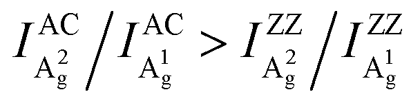 . In-depth analysis based on the quantum theory of the first-order Raman scattering shows that the ratio
  is only related to the intrinsic phonon-mode dependent electron–phonon coupling in BP. Combined with the specific atomic vibration patterns of the two Ag phonons, the physical origin of the inequality is revealed and further supported by density functional theory (DFT) calculations on the Raman tensors of both Ag modes.
Results and discussion
The crystal structure of BP from different perspectives is illustrated in Fig. 1a. Similar to the conventional definition of the crystallographic axes of BP, the x- and z-axes are along the AC and ZZ directions, respectively.33 To obtain comparable reference directions, the crystal orientations of a BP flake with different thickness regions (Fig. 1b) were first determined by high-resolution transmission electron microscopy (HRTEM). The diffraction pattern and the HRTEM image allow us to identify the AC and ZZ directions,7 as labeled in Fig. 1b and c.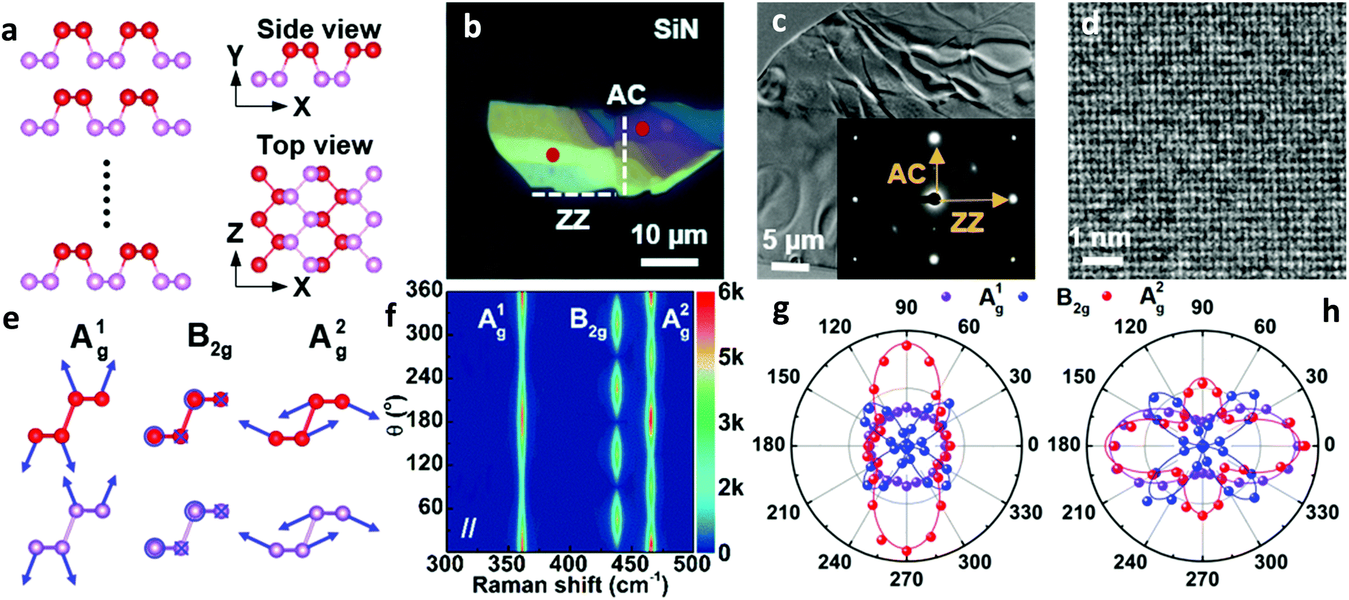 | ||
| Fig. 1 (a) Schematic illustration of BP crystal structure from different perspectives. The upper and lower rows of phosphor atoms are differentiated using red and violet colors, respectively. (b) Optical image of a BP flake with different thicknesses for combined HRTEM/Raman measurements. The red dots mark the positions where the ARPRS data of (g) and (h) were collected. (c) TEM image of the BP flake with the inset showing its corresponding diffraction patterns. (d) HRTEM image of the same flake. (e) Atomic displacements of the A1g, B2g and A2g phonon modes. (f) False-color plot of polarized Raman intensities collected from the purple region labeled in (b) by a 532 nm laser. (g and h) Corresponding polar plots of the three modes taken from the two red dots in the (g) light yellow region and (h) purple region shown in (b). | ||
To further explore how to determine the crystal orientations through ARPRS, polarized Raman measurements were then performed on two regions with different colors of the same BP flake, labeled by red dots in Fig. 1b. ARPRS under different rotation angles θ (the angle between the laser polarization direction and the ZZ direction) was collected under the parallel polarization configuration. Fig. 1f shows a false-color plot of polarized Raman intensities collected from the purple region by a 532 nm laser. Under the backscattering geometry, three peaks at 361, 438 and 466 cm−1 correspond to the A1g, B2g and A2g phonon modes and represent the out-of-plane vibration (A1g), and in-plane vibrations along the ZZ (B2g) and AC (A2g) directions, respectively (Fig. 1e). Fig. 1g and h show the ARPRS responses of all of three modes sampled in the light yellow (∼40 nm thick) and purple (∼70 nm thick) regions, respectively (see the ESI,† Fig. S1 for the series of Raman spectra). We observe that for the two sampled regions, the main axes of the polar plots are along different directions: for the light-yellow region, the main axis of A2g is along the AC direction while the ARPRS response of A1g is almost isotropic (Fig. 1g). As for the purple region, the main axes of both Ag modes are along the ZZ direction (Fig. 1h). Therefore, the crystal orientations of BP cannot be solely determined via the ARPRS response of a single phonon mode as it may give conflicting assignments. However, we observe that the Raman peak intensity ratios of the two Ag modes are different along the ZZ and AC directions, which satisfy the inequality  for both regions. In the polar plot, the ARPRS intensity as a function of θ for the Ag modes can be fitted by (see the ESI,† Calculations section for detailed discussion on ARPRS intensity fitting),
I‖(Ag) = a2![[thin space (1/6-em)]](https://www.rsc.org/images/entities/char_2009.gif) sin4θ + c2cos4θ + 2acsin2θcos2θ sin4θ + c2cos4θ + 2acsin2θcos2θ![[thin space (1/6-em)]](https://www.rsc.org/images/entities/i_char_2009.gif) cosϕca cosϕca | (1) |
This expression relates the Raman intensities at the two crystal axis directions to the Raman tensor elements. We noticed that recently, Lin et al.29 proposed a model to fit the ARPRS intensity of ALMs via only the real Raman tensor by considering birefringence and linear dichroism effects; this provides a new perspective for the controversial issue23,26,29 of ARPRS intensity fitting of ALMs. However, the complete settlement of this dispute may still require follow-up work, given that complex Raman tensor elements might actually occur for materials excited in the absorption regime. And, the birefringence effect can be neglected for opaque absorbent materials34 including BP. The linear dichroism effect is usually considered by including a phase factor in the Raman tensor elements, as the imaginary parts are a direct consequence of the optical absorption in BP.23 Therefore, in our work, we adopt the widely used method of Raman tensor with a phase factor (i.e., complex Raman tensor elements)23 to understand the ARPRS intensity.
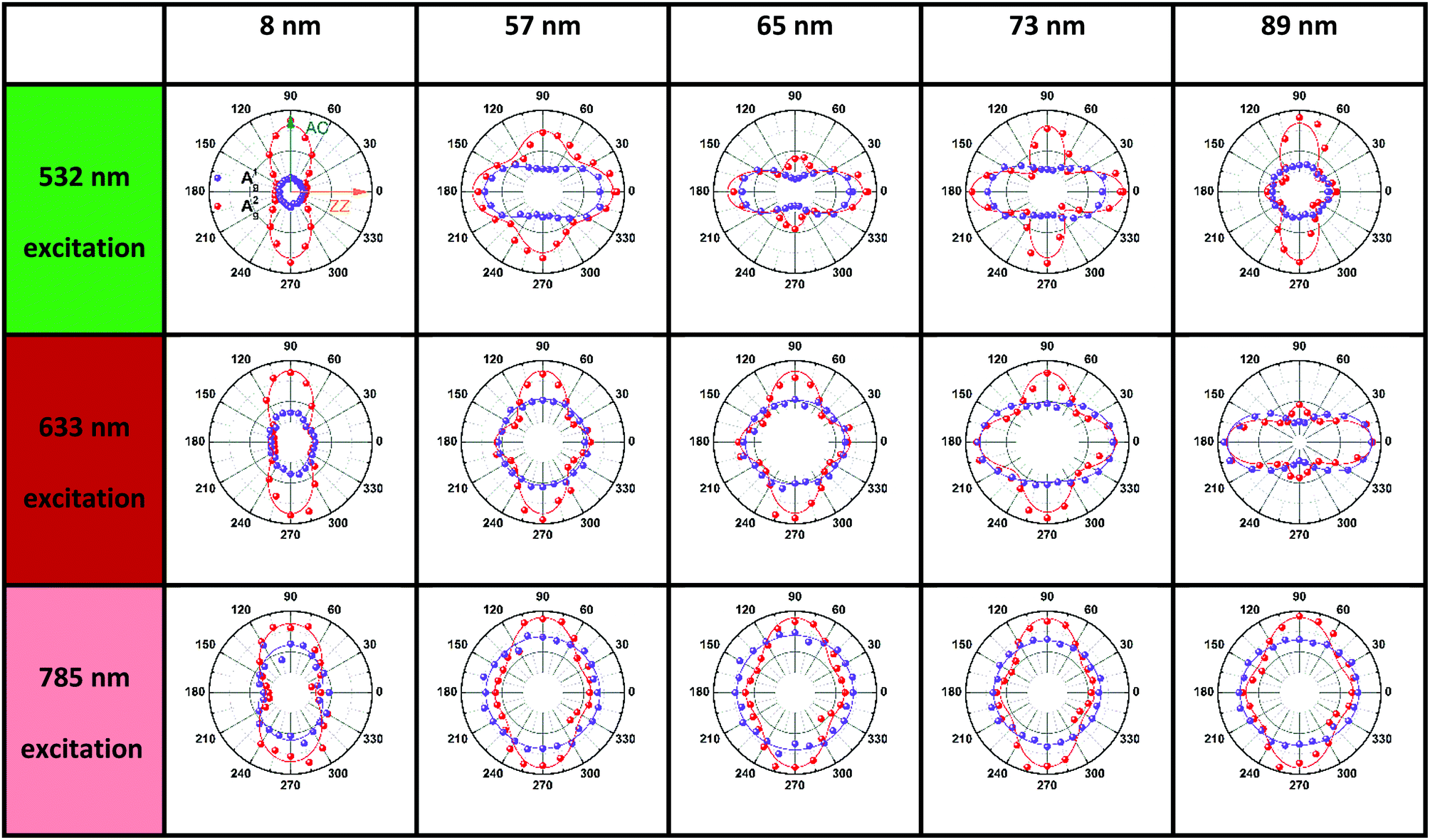
To further study the intricate ARPRS response and clarify its physical origin, as well as to test whether the inequality  is universally applicable, we performed thickness and excitation wavelength dependent ARPRS measurements on a series of BP flakes (see the ESI,† Fig. S2 for the optical images). Table 1 shows the ARPRS responses of both Ag modes for five representative regions with thicknesses ranging from 8–89 nm; the complete series of experimental results (8–170 nm) are available in the ESI,† Table S1.
|
It is evident in Table 1 and Table S1 (ESI†) that the main axes of the ARPRS responses of both Ag modes alternate between the AC and ZZ directions by changing the sample thickness and excitation wavelength. Moreover, this switching occurs in a gradual and periodic manner as the sample thickness increases. Taking the 532 nm excitation results as an example, for the ultrathin 8 nm flake, the main axes of the ARPRS responses for both A1g and A2g are along the AC direction (90° and 270°). When the flake thickness is between 12 and 43 nm, the main axes of responses of A2g are still along 90° and the degree of anisotropy of the responses is almost unchanged but the response of A1g is almost isotropic at 43 nm. When the flake thickness increases to 52 nm, the main axis of A1g is flipped to the ZZ direction (0° and 180°); secondary maxima at 0° and 180° begin to appear in the response of A2g and their intensities increase with the flake thickness. For the 57 nm flake, the Raman intensities of A2g along the ZZ direction increase to almost equal to those along the AC direction, implying an isotropic-like ARPRS response of the A2g mode. For the 60 nm flake, the main axis of the polar plot of A2g is changed to along the ZZ direction, which is perpendicular to the initial AC direction for the 8 nm flake. Thus far the main axis switching process of A2g is also completed. This process occurs periodically as the flake thickness continues to increase and the results under 633 and 785 nm excitation wavelengths follow a similar evolution. It is worth mentioning that the phenomenon is more obvious in the response under the 532 and 633 nm excitations, but not in the 785 nm excitation result. This will be discussed in detail later.
Although similar main axis switching phenomena were observed in previous reports,23–26,28 its detailed evolutionary manner remained undiscovered. Our findings reveal for the first time that this switching occurs in a gradual and periodic way and therefore it must experience a critical thickness (before switching) at which the ARPRS response is isotropic-like, such as the response of A2g of the 57 nm flake under the 532 nm excitation and the response of A1g of the same flake under the 633 nm excitation. Such responses make powerless the traditional single phonon mode method for identifying crystal orientations. However, the universal applicability of the inequality  has been preserved irrespective of the sample thickness and laser wavelength, which indicates that it can be used to unambiguously distinguish the AC and ZZ directions of BP. All these crucial observations, including the gradual and periodic evolution of the response, the isotropic-like responses at the critical thicknesses, and the universality of the Raman peak intensity ratio method, benefit from our systematic ARPRS study, especially its thickness dependence based on a large number of BP samples with thickness intervals of a few nanometers.
To analyze the physical origin of the intricate ARPRS response, the Raman tensor anisotropy ratio c/a, which can quantify the degree of anisotropy of the response, was extracted from each polar plot of the angle-resolved Raman intensity. The thickness-dependent profiles of c/a (c/a-profiles) of both Ag modes (c1/a1 for A1g mode and c2/a2 for A2g mode) are shown in Fig. 2 for the (a) 532 nm, (b) 633 nm, and (c) 785 nm excitations. The measured c/a values of both Ag modes change periodically with the flake thickness for all three laser wavelengths as mentioned earlier, exhibiting obvious interference peak-like features that redshift as the laser wavelength increases. Excitingly, the c/a-profiles are in good alignment with the calculated thickness-dependent profiles of the interference enhancement factors ratio (FZZ/FAC) using wavelength-dependent refractive index data of BP by electron energy-loss spectroscopy,35 especially the peak position, as shown in Fig. 2a–c (see the ESI,† Fig. S4 for the comparison of fittings using refractive index values from different literature reports). This reveals directly and convincingly that the anisotropic interference effect is the dominant mechanism for the thickness-dependent ARPRS response and is responsible for the main axis switching phenomenon in the ARPRS response of BP. The fluctuation of c/a values on both sides of unity correlates to the main axis switching of BP's ARPRS response, as illustrated in the ESI,† Table S1. This is clearly observed especially for the 532 and 633 nm excitations, which is attributed to a sufficiently large FZZ/FAC value as a result of the wavelength-dependent, strong linear dichroism (see the ESI,† Table S2). For the 785 nm laser, however, the linear dichroism or thereby FZZ/FAC is small, so the c2/a2 values are always below 1 within the thickness range of our experiment and thus the main axes remain along the AC direction (Fig. 2c). The anisotropic interference effect governed by the wavelength-dependent linear dichroism provides an important perspective to predict the thickness-dependent ARPRS response of ALMs. Once the wavelength dependent anisotropic complex refractive index of ALMs is known, we can infer in which material and at which excitation wavelength the main axis switching phenomenon is more prone to appear. Therefore, caution must be taken when the ARPRS response is used for crystal orientation identification like the case of BP.
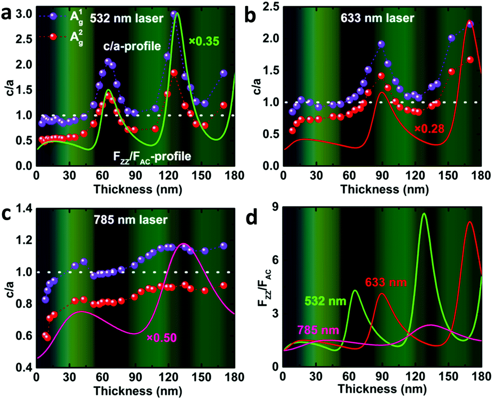 | ||
| Fig. 2 Thickness-dependent anisotropy ratio (dots) c/a of the two Ag modes measured under (a) 532 nm, (b) 633 nm and (c) 785 nm excitations. The dotted lines serve as a guide to the eye. The solid line represents the thickness-dependent interference enhancement factors ratio FZZ/FAC. The horizontal dashed lines at c/a = 1 in (a)–(c) represent the isotropic-like case for the ARPRS response. The color charts in the backgrounds of (a)–(d) correspond to the true colors of BP flakes with different thicknesses measured by AFM. (d) Calculated FZZ/FAC as a function of the BP thickness on a SiO2(300 nm)/Si substrate for different excitation wavelengths. | ||
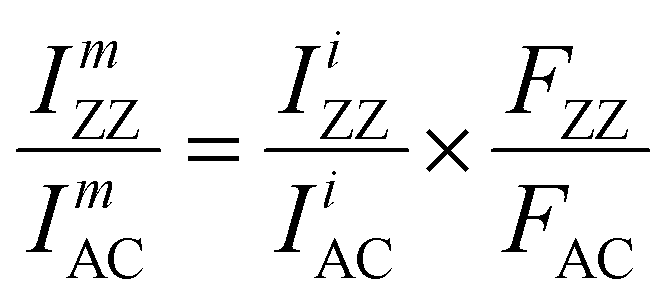
Following previous reports,24,36 the calculation details of FZZ/FAC are available in the Experimental section. As shown in eqn (6) in the Experimental section, the interference enhancement factor (F) consists of two parts, the normalization factor N (reciprocal number of the enhancement factor for a free-standing BP, obtained by replacing the SiO2 and Si layers with air) and the integral term. However, a disagreement lies in whether to include the influence of N in the calculation of F. It was included in some studies24,25,36,37 but absent in other reports.28,38,39 We point out that when the measured Raman intensity is corrected with the integral term, the obtained Raman intensity is intrinsic and only relates to electron-photon and electron–phonon interactions. In contrast, the one corrected by eqn (6) is not intrinsic, but still contains the influence of interference enhancement effect brought by the upper and lower surfaces of the sample itself.
In order to clarify whether the sample itself or the substrate contributes more to the interference enhancement on the Raman spectrum of BP, we calculated the total enhancement factor (the integral term), the enhancement factor brought by the sample (1/N), and the enhancement factor brought by the substrate (eqn (6)), as shown in the ESI,† Fig. S5. We clearly see that the interference enhancement brought by the BP flake itself is far greater than that brought by the substrate and is the main source of the interference enhancement. Therefore, the normalization factor N cannot be included in the enhancement factor calculations. These results also indicate that the interference effect cannot be effectively eliminated by replacing the SiO2/Si substrate with a transparent substrate (such as quartz and sapphire)26,40 or suspending the BP flake.
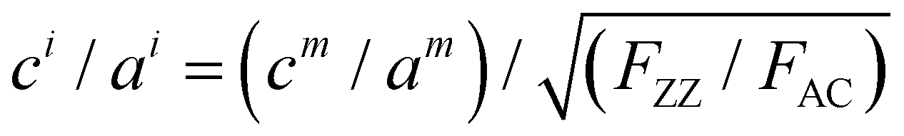
To further verify this, we transferred a BP flake with different thickness regions to a SiO2/Si substrate with prefabricated microwells as shown in Fig. 3a. The collected ARPRS responses from both the suspended and supported BP regions with different thicknesses are shown in Fig. 3b–f. These results show that the suspended and supported BP regions have similar ARPRS responses, i.e., the main axes of the polar plots are along the same direction and the degrees of anisotropy are almost equal as also evidenced by the c/a profiles in the ESI,† Fig. S6. The only difference is that the Raman intensity of the supported BP is slightly larger than that of the suspended one due to the slight interference enhancement brought by the substrate (see the ESI,† Fig. S5). In the c/a profile of the suspended BP in Fig. S6 (ESI†), the interference peak-like features still exist, which well proved the aforementioned conclusion that the interference enhancement effect cannot be eliminated experimentally for BP. Nevertheless, the thickness independent intrinsic c1/a1 and c2/a2 values can be obtained once the anisotropic interference enhancement is accurately eliminated via dividing the measured c/a values by  (see eqn (8) in Experimental section for details). In principle, the intrinsic Raman intensities at all angles can be obtained using the angle-dependent complex refractive index of BP. However, this method is cumbersome and time-consuming.
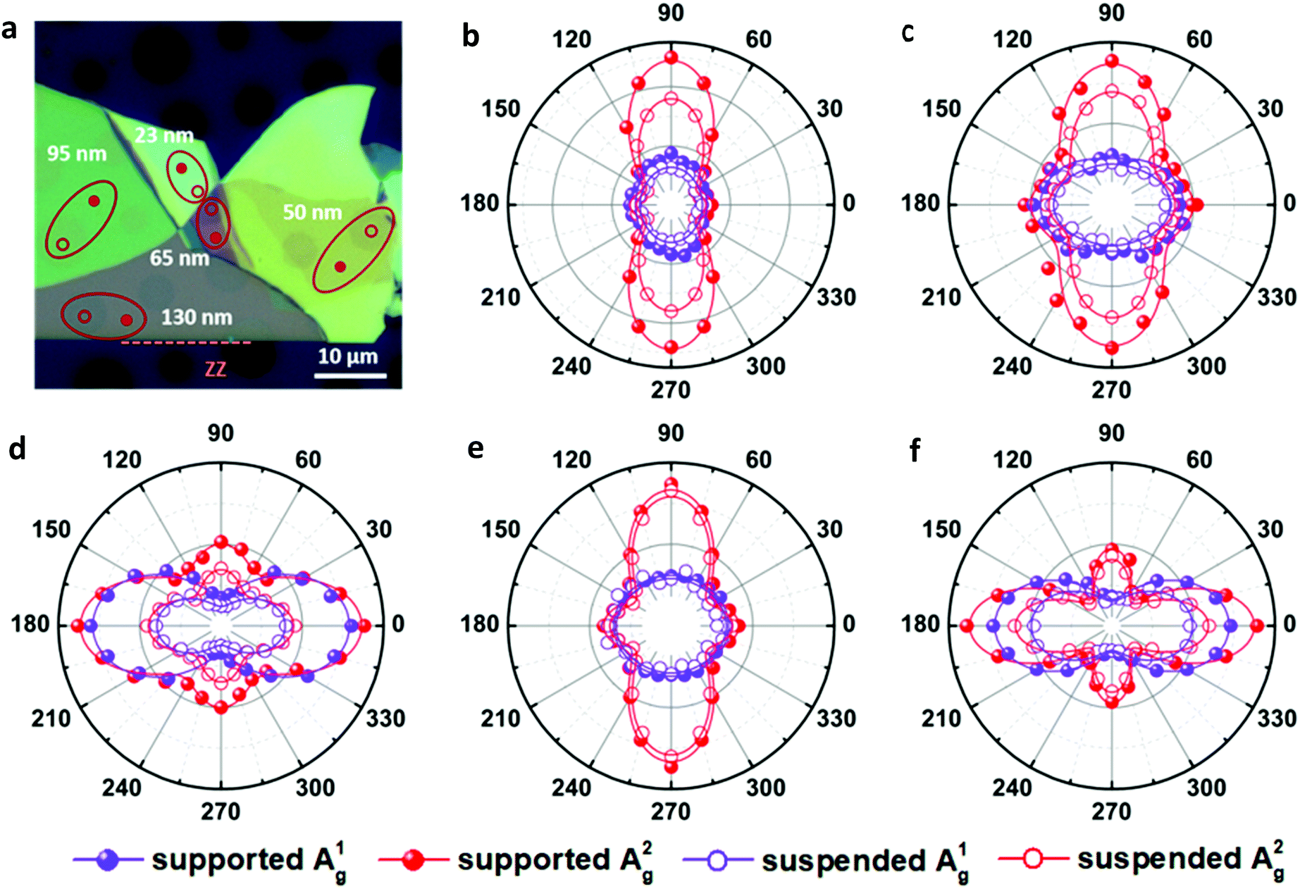 | ||
| Fig. 3 (a) Optical image of a BP flake with regions of different thicknesses suspended on a SiO2/Si substrate with hole arrays of different diameters (3–6 μm). ARPRS responses collected from both the suspended and supported BP regions of (b) 23 nm, (c) 50 nm, (d) 65 nm, (e) 95 nm and (f) 130 nm thick by a 532 nm laser. | ||
Despite the variation of c/a with the thickness for both Ag modes as shown in Fig. 2a–c and Fig. S5 (ESI†), the c/a value of the A1g mode is always greater than that of A2g regardless of the flake thickness and excitation wavelength, i.e., c1/a1 > c2/a2. This implies that the inequality may reflect a certain intrinsic property of BP. For the same excitation wavelength, the different intrinsic values of c1/a1 and c2/a2 represent the phonon-mode dependence of BP's ARPRS response. Taking the 532 nm excitation result (Fig. 2a) as an example, the c1/a1 ∼ 0.9 and c2/a2 ∼0.5 in thin regions (< 40 nm) represent the intrinsic anisotropy ratios of the two modes, respectively, as the interference enhancement factor ratio FZZ/FAC is near unity. Our ARPRS measurement of bulk BP also proved this (see the ESI,† Fig. S7 for experimental results and detailed discussion). Furthermore, an important conclusion that can be drawn from c1/a1 > c2/a2 is that a2/a1 > c2/c1, or  . This concise inequality can be readily used to determine crystal orientations of both BP nanoflakes and bulk BP (see the ESI,† Fig. S7), and the physical origin lies in the phonon-mode dependence of the ARPRS response as discussed next The extracted a2/a1 and c2/c1 are shown in Fig. 4a. In comparison with c1/a1 and c2/a2 in Fig. 2a–c, the most significant difference is that a2/a1 and c2/c1 no longer have a thickness dependence. Moreover, the a2/a1 and c2/c1 values both have laser wavelength dependence, that is, both decrease with a decreasing incident photon energy. As shown in the statistical images of Fig. 4b and c, Gaussian fittings show that the values of a2/a1 are around 1.66, 1.33 and 1.14 and c2/c1 around 1.08, 1.01 and 0.91, respectively, for the 532, 633, and 785 nm lasers. To understand the physics behind these measured values, we conducted an in-depth analysis based on the quantum theory of the first-order Raman scattering and first-principles calculations of the laser wavelength-dependent Raman tensors.
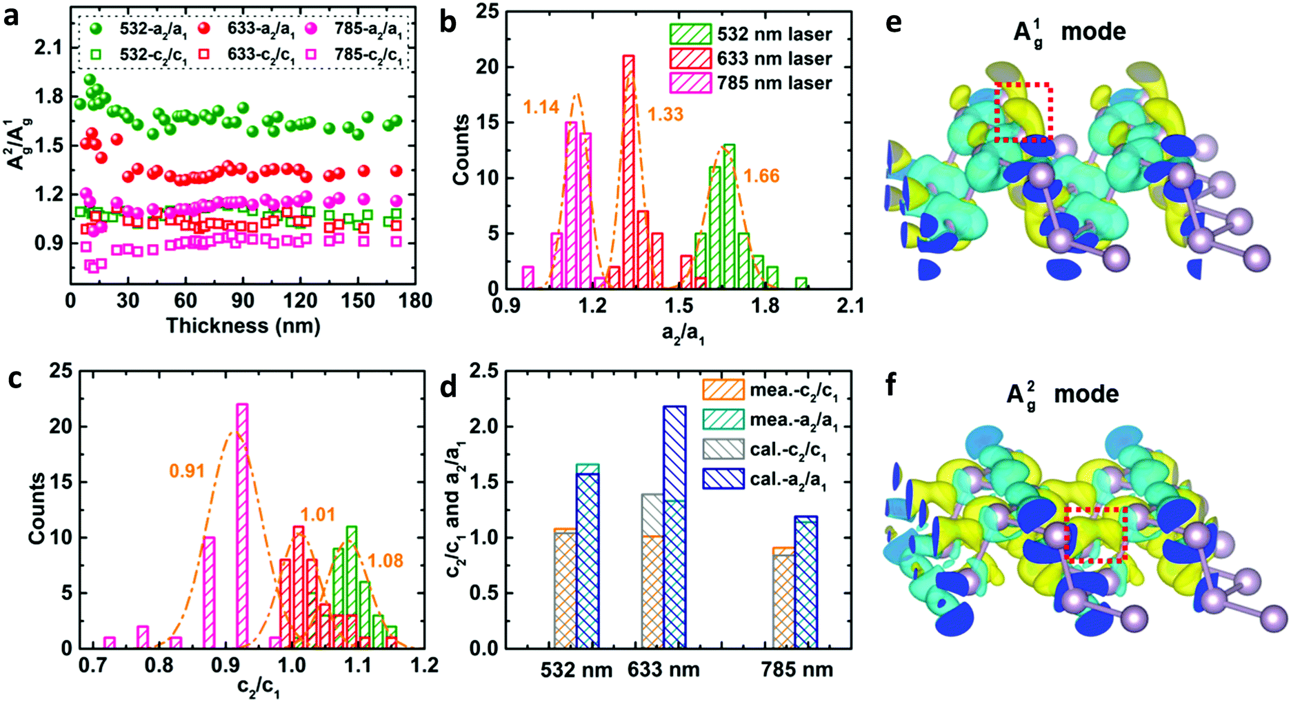 | ||
| Fig. 4 (a) Measured thickness- and laser wavelength-dependent ratios a2/a1 and c2/c1. Statistical images and corresponding Gaussian fittings of (b) a2/a1 and (c) c2/c1 under 532, 633, and 785 nm laser excitations. (d) DFT calculated values and Gaussian statistical values of a2/a1 and c2/c1. The electron charge density difference of the conduction band states before and after the atomic vibration of the (e) A1g and (f) A2g phonon modes. Yellow and blue isosurfaces correspond to positive and negative values of 2.37 × 10⁻⁴ e Å−3, respectively. | ||
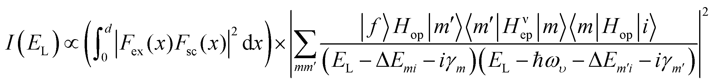
The laser energy (EL) dependent intrinsic first-order Raman scattering intensity I(EL) can be calculated using the perturbation theory.41,42 Given that the extrinsic optical interference effect will also significantly affect the Raman intensity of 2D materials as proven above and elsewhere,24,36,37 the actual Iν(EL) measured for a phonon mode ν should be:
 | (2) |
Eqn (2) reveals that the influencing factors of the Raman intensity include two optical processes: internal optical absorption and external interference. For BP, the wavelengths of Raman scattered light for the two Ag phonon modes are very close (see the ESI,† Table S2). The optical absorption at these two scattering wavelengths is approximately identical since there is no singularity in the absorption spectrum.13 Moreover, the interference enhancement factors calculated using the complex refractive index at these two wavelengths are nearly equal (see the ESI,† Fig. S8). Therefore, the above two optical effects will be eliminated without knowing their quantitative information once the Raman peak intensity ratio IAg2/IAg1 is constructed. Then this ratio is mainly related to the intrinsic electron–phonon coupling, given by the 〈m′|Hυep|m〉 term. For thicker BP flakes, the electron–phonon coupling is similar to bulk BP owing to the similar electronic structures, so the ratios a2/a1 and c2/c1 no longer have a thickness dependence (Fig. 4a). We note that the Raman peak intensity ratios or Raman tensor element ratios between different phonon modes not only can be potentially used to determine the crystal orientations, but also can provide a perspective for quantifying the relative strength of the phonon-mode dependent electron–phonon coupling. The study of electron–phonon coupling is crucial in fully revealing the physical origin of the ARPRS response of ALMs (especially for those having multiple Raman modes) and in understanding the electrical and thermal transport properties of ALMs.
To gain further insights into the measured values of a2/a1 and c2/c1 and their laser wavelength dependence, the intrinsic Raman tensors of both Ag modes were calculated by DFT calculations according to eqn (3) (see the Experimental section for details).43–45 The calculation results, shown in Table S3 (ESI†), are quantitatively or semi-quantitatively consistent with the experimental results (Fig. 4d). According to eqn (3), the Raman tensor is determined by the variation of the corresponding dielectric tensor component, i.e., the difference of the dielectric tensor components before and after the atomic vibration. The electron charge density differences of the conduction band states of both Ag modes are shown in Fig. 4e and f, respectively. Although both Ag modes involve coupled in-plane and out-of-plane atomic vibrations, the A2g phonon has a larger vibrational component along the in-plane AC direction while the A1g phonon mainly vibrates along the out-of-plane direction (Fig. 1e). Therefore, the electron clouds are mainly modulated vertically (along the out-of-plane direction) or laterally (along the AC direction) by the movements of the phosphorus atoms for the A1g or A2g phonon, respectively (Fig. 4e and f). In this way, the phonon induced charge density difference, and thus the change in the dipole moment or in the dielectric tensor component along the AC direction (Δεxx) of the A2g phonon is greater than that of the A1g phonon (a2 > a1). However, the changes in the dielectric tensor component along the ZZ direction (Δεzz) of the two phonon modes are comparable (c2 ≈ c1) (see the ESI,† Fig. S9 for schematic diagram to aid understanding). This leads to the inequality a2/a1 > c2/c1. In addition, the frequency-dependent Raman tensor element ratios are ascribed to the frequency-dependent dielectric tensor when the incident photon energy is far from resonance, which is at about 2.72 eV for the incident resonance (EL − ΔEmi − iγm) corresponding to the beginning of dipole transitions from the valence 3p states to the conduction ones.46
Experimental
Sample fabrication and characterization
BP flakes with thicknesses from 8 nm to ∼170 nm were prepared by standard mechanical exfoliation from a bulk BP single crystal (purchased from Shanghai ONWAY technology Co., Ltd) and then dry transferred to a 300 nm SiO2/Si substrate. Exfoliated BP flakes were also transferred onto a SiO2/Si substrate with hole arrays to obtain suspended BP samples. The morphology, color and the thickness of each BP film were characterized by optical microscopy and atomic force microscopy.Raman and TEM characterization
Raman spectra were collected on a Renishaw InVia Raman Microscope system equipped with three laser lines (532, 633, and 785 nm). A 100× objective and 1800 lines per mm (for 532 nm, 633 nm lasers) and 1200 lines per mm (for 785 nm laser) gratings were used to collect Raman signals. For the polarization-dependence Raman measurements, a polarizer was placed between the edge filter and the detector to obtain the parallel polarization configuration. The sample was mounted on a custom-built rotation stage, and polarized Raman spectra with different angles were obtained by rotating the sample with a step of 15°. To prevent degradation of BP samples, the humidity of the laboratory environment was controlled to be lower than 40% and all measurements were taken immediately after sample preparation. For TEM characterization, a BP flake was directly transferred onto an amorphous holey silicon nitride (SiNx) TEM grid. HRTEM images and selected-area diffraction images were taken in a JEM-3200FS TEM operated at 300 kV.DFT calculations
Density functional theory (DFT) calculations were performed with the Vienna Ab initio Simulation Package (VASP). The exchange–correlation interactions were treated using the Perdew–Burke–Ernzerhof (PBE) approximation.47 Projected Augmented Waves (PAW) pseudopotentials were used for electron–ion interactions.48,49 van der Waals (vdW) interactions between layers were considered with density functional method optB86b-vdW.50 Vacuum slabs of 10.37 Å thick were inserted between neighboring 2D atom layers. The cutoff energy was taken as 500 eV. The convergence value for electronic relaxation was 1 × 10⁻⁵ eV per atom. During the optimization process, the total force on each atom was less than 1 × 10⁻³ eV Å−1. A 12 × 4 × 9 Monkhorst k-point mesh was used for the optimization and electron relaxation process. Raman tensor calculations were performed using an optimized bulk BP structure. The dynamic matrix was first calculated using the finite difference scheme implemented in the Phonopy software.51 Hellmann–Feynman forces (the second-order force constants) of a 3 × 1 × 3 supercell were computed by VASP for both positive and negative atomic displacements (δ = 0.005 Å) and then used in Phonopy to construct the dynamic matrix. The diagonalization of the dynamic matrix provides phonon frequency (its square is the eigenvalue of the dynamic matrix), and phonon eigenvector (i.e., vibration). The matrix elements of the (3 × 3) Raman tensor for the jth phonon mode at incident laser energy EL is given by43–45,52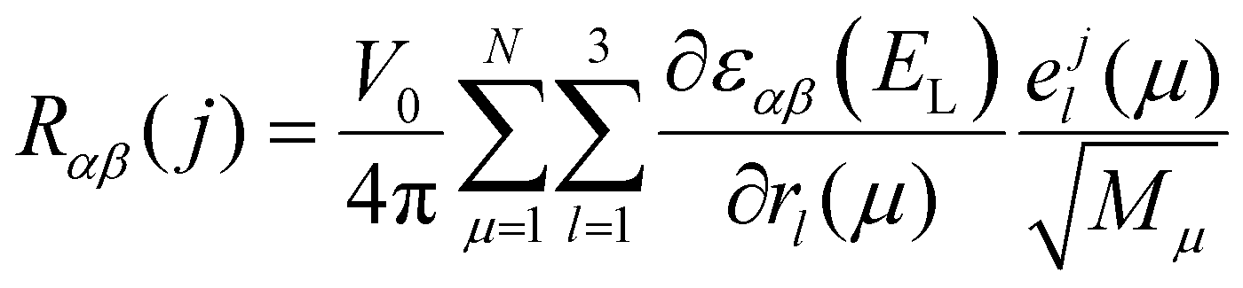 | (3) |
 is the first derivative of the dielectric tensor with respect to the atomic displacement. For both positive and negative atomic displacements (δ = 0.005 Å) in the unit cell, the dielectric tensor of the structure with finite displacement was calculated by DFT at the chosen laser energy using a 24 × 4 × 18 grid, and 48 empty bands. Then, the derivatives were obtained by the finite difference scheme. Based on the phonon frequencies, phonon eigenvectors, and the derivatives of dielectric tensors, the Raman tensor of any phonon mode at any laser energy can be obtained. The calculated wavelength-dependent intrinsic Raman tensors of both Ag phonon modes and the Raman-tensor ratios between different modes are shown in the ESI,† Table S3, which matches the experimental results well.
Interference enhancement factor calculations
For thin two-dimensional (2D) materials on SiO2/Si substrates, when the thickness of the 2D material or the substrate is comparable with the wavelength of light, the optical interference effect can significantly enhance the Raman intensity due to multiple reflections inside the 2D material layer as well as in the SiO2 layer.36 Taking BP as an example, the net enhancement of incident light Fex(x) caused by multiple reflections at a position x measured from the BP surface is given by36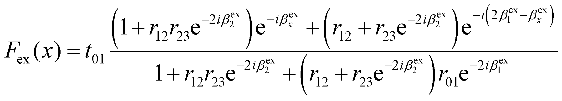 | (4) |
The net enhancement of scattered light Fsc(x) is given by36
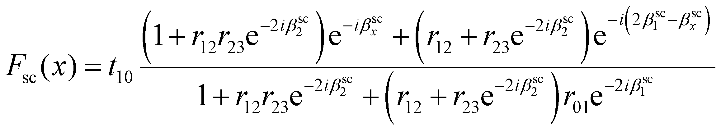 | (5) |
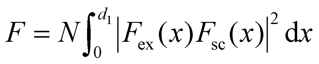 | (6) |
 | (7) |
 | (8) |
 .
.
Conclusions
In conclusion, we delved into the intricate ARPRS response of BP flakes. Based on the extensive experiments, for the first time, the main axes switching phenomenon in the ARPRS response is directly observed as a consequence of significant anisotropic interference effect led by the strong linear dichroism in BP. Additionally, the interference effect cannot be effectively eliminated experimentally as the interference enhancement on the Raman signal mainly comes from the BP flake itself, but it can be eliminated by the Raman peak intensity ratio between the A1g and A2g modes. We also demonstrated that the AC and ZZ directions of BP can be unambiguously distinguished by the Raman peak intensity ratios via a concise inequality . In-depth quantum perturbation theory analysis and first-principles calculations on the intrinsic Raman tensor reveal that the physical origin lies in the phonon-mode dependent electron–phonon coupling. Our findings have resolved the two key disputes in BP's ARPRS response. The integrated generic method we proposed paves the way for fully understanding and even predicting the ARPRS response of various anisotropic layered materials; and can also facilitate chirality-relevant studies and future device applications of them.
Author contributions
B. Z. and H. S. conceived the idea of using the Raman intensity ratio to distinguish the crystal orientations in BP. B. Z., Y. Z., D. K., and H. S. designed the experiments. B. Z. and M. Z. prepared the BP samples and performed the AFM characterization. B. Z. performed the ARPRS measurement. Y. W. and W. L. performed the first-principles calculations of Raman tensors. X. Z., C.-T. Y., and X. C. contributed to the analysis and interpretation of the data. B. Z., Y. W. and H. S. wrote the manuscript with input from other authors. All authors have given approval to the final version of the manuscript.Conflicts of interest
The authors declare no competing financial interests.Acknowledgements
This work was supported by the Natural Science Foundation of Guangdong Province (grant no. 2020A1515010885) and the Shenzhen Science and Technology Innovation Program (grant no JCYJ20190806142614541). The authors are grateful to F. Yen, S. Chen and Z. Li (Harbin Institute of Technology, Shenzhen) for helpful discussions and J. Xiao, Z. Liu, Z. Peng, and H. Li (Renishaw) for hardware and technical support. We are also grateful to J. Wang and Z. Cheng (Shenzhen Institute of Advanced Technology, Chinese Academy of Sciences) for providing the bulk BP sample used for manuscript revision.References
- H. Liu, A. T. Neal, Z. Zhu, Z. Luo, X. Xu, D. Tomek and P. D. Ye, ACS Nano, 2014, 8, 4033–4041 CrossRef CAS PubMed.
- T. Low, R. Roldan, H. Wang, F. Xia, P. Avouris, L. M. Moreno and F. Guinea, Phys. Rev. Lett., 2014, 113, 106802 CrossRef PubMed.
- J. Guan, Z. Zhu and D. Tomanek, Phys. Rev. Lett., 2014, 113, 046804 CrossRef CAS PubMed.
- F. Liu, H. Shimotani, H. Shang, T. Kanagasekaran, V. Zólyomi, N. Drummond, V. I. Faíko and K. Tanigaki, ACS Nano, 2014, 8, 752–760 CrossRef CAS PubMed.
- S. Tongay, H. Sahin, C. Ko, A. Luce, W. Fan, K. Liu, J. Zhou, Y. S. Huang, C. H. Ho, J. Yan, D. F. Ogletree, S. Aloni, J. Ji, S. Li, J. Li, F. M. Peeters and J. Wu, Nat. Commun., 2014, 5, 3252 CrossRef PubMed.
- L. Li, Y. Yu, G. J. Ye, Q. Ge, X. Ou, H. Wu, D. Feng, X. H. Chen and Y. Zhang, Nat. Nanotechnol., 2014, 9, 372–377 CrossRef CAS PubMed.
- J. Qiao, X. Kong, Z. X. Hu, F. Yang and W. Ji, Nat. Commun., 2014, 5, 4475 CrossRef CAS PubMed.
- F. Xia, H. Wang and Y. Jia, Nat. Commun., 2014, 5, 4458 CrossRef CAS.
- A. N. Rudenko, S. Brener and M. I. Katsnelson, Phys. Rev. Lett., 2016, 116, 246401 CrossRef CAS PubMed.
- X. Wang, A. M. Jones, K. L. Seyler, V. Tran, Y. Jia, H. Zhao, H. Wang, L. Yang, X. Xu and F. Xia, Nat. Nanotechnol., 2015, 10, 517–521 CrossRef CAS PubMed.
- Z. Luo, J. Maassen, Y. Deng, Y. Du, R. P. Garrelts, M. S. Lundstrom, P. D. Ye and X. Xu, Nat. Commun., 2015, 6, 8572 CrossRef CAS PubMed.
- J. W. Jiang and H. S. Park, Nat. Commun., 2014, 5, 4727 CrossRef CAS PubMed.
- V. Tran, R. Soklaski, Y. Liang and L. Yang, Phys. Rev. B: Condens. Matter Mater. Phys., 2014, 89, 235319 CrossRef.
- A. S. Rodin, A. Carvalho and A. H. Castro Neto, Phys. Rev. Lett., 2014, 112, 176801 CrossRef CAS PubMed.
- Z. J. Xiang, G. J. Ye, C. Shang, B. Lei, N. Z. Wang, K. S. Yang, D. Y. Liu, F. B. Meng, X. G. Luo, L. J. Zou, Z. Sun, Y. Zhang and X. H. Chen, Phys. Rev. Lett., 2015, 115, 186403 CrossRef CAS PubMed.
- S. Huang, F. Wang, G. Zhang, C. Song, Y. Lei, Q. Xing, C. Wang, Y. Zhang, J. Zhang, Y. Xie, L. Mu, C. Cong, M. Huang and H. Yan, Phys. Rev. Lett., 2020, 125, 156802 CrossRef CAS.
- K. F. Mak, C. Lee, J. Hone, J. Shan and T. F. Heinz, Phys. Rev. Lett., 2010, 105, 136805 CrossRef PubMed.
- L. Peng, S. A. Wells, C. R. Ryder, M. C. Hersam and M. Grayson, Phys. Rev. Lett., 2018, 120, 086801 CrossRef CAS PubMed.
- D. A. Chenet, O. B. Aslan, P. Y. Huang, C. Fan, A. M. van der Zande, T. F. Heinz and J. C. Hone, Nano Lett., 2015, 15, 5667–5672 CrossRef CAS.
- Y. Choi, K. Kim, S. Y. Lim, J. Kim, J. M. Park, J. H. Kim, Z. Lee and H. Cheong, Nanoscale Horiz., 2020, 5, 308–315 RSC.
- J. Wu, N. Mao, L. Xie, H. Xu and J. Zhang, Angew. Chem., Int. Ed., 2015, 54, 2366–2369 CrossRef CAS PubMed.
- W. Lu, X. Ma, Z. Fei, J. Zhou, Z. Zhang, C. Jin and Z. Zhang, Appl. Phys. Lett., 2015, 107, 021906 CrossRef.
- H. B. Ribeiro, M. A. Pimenta, C. J. S. de Matos, R. L. Moreira, A. S. Rodin, J. D. Zapata, E. A. T. de Souza and A. H. Castro Neto, ACS Nano, 2015, 9, 4270–4276 CrossRef CAS PubMed.
- J. Kim, J. U. Lee, J. Lee, H. J. Park, Z. Lee, C. Lee and H. Cheong, Nanoscale, 2015, 7, 18708–18715 RSC.
- X. Ling, S. Huang, E. H. Hasdeo, L. Liang, W. M. Parkin, Y. Tatsumi, A. R. Nugraha, A. A. Puretzky, P. M. Das, B. G. Sumpter, D. B. Geohegan, J. Kong, R. Saito, M. Drndic, V. Meunier and M. S. Dresselhaus, Nano Lett., 2016, 16, 2260–2267 CrossRef CAS PubMed.
- N. Mao, J. Wu, B. Han, J. Lin, L. Tong and J. Zhang, Small, 2016, 12, 2627–2633 CrossRef CAS.
- A. L. Phaneuf-L'Heureux, A. Favron, J. F. Germain, P. Lavoie, P. Desjardins, R. Leonelli, R. Martel and S. Francoeur, Nano Lett., 2016, 16, 7761–7767 CrossRef.
- N. Mao, X. Wang, Y. Lin, B. G. Sumpter, Q. Ji, T. Palacios, S. Huang, V. Meunier, M. S. Dresselhaus, W. A. Tisdale, L. Liang, X. Ling and J. Kong, J. Am. Chem. Soc., 2019, 141, 18994–19001 CrossRef CAS.
- M.-L. Lin, Y.-C. Leng, X. Cong, D. Meng, J. Wang, X.-L. Li, B. Yu, X.-L. Liu, X.-F. Yu and P.-H. Tan, Sci. Bull., 2020, 65, 1894–1900 CrossRef CAS.
- Y. Hsiao, P.-Y. Chang, K.-L. Fan, N.-C. Hsu and S.-C. Lee, AIP Adv., 2018, 8, 105216 CrossRef.
- B. Deng, V. Tran, Y. Xie, H. Jiang, C. Li, Q. Guo, X. Wang, H. Tian, S. J. Koester, H. Wang, J. J. Cha, Q. Xia, L. Yang and F. Xia, Nat. Commun., 2017, 8, 14474 CrossRef CAS PubMed.
- G. Abellan, S. Wild, V. Lloret, N. Scheuschner, R. Gillen, U. Mundloch, J. Maultzsch, M. Varela, F. Hauke and A. Hirsch, J. Am. Chem. Soc., 2017, 139, 10432–10440 CrossRef CAS.
- S. Sugai, T. Ueda and K. Murase, J. Phys. Soc. Jpn., 1981, 50, 3356 CrossRef CAS.
- C. Kranert, C. Sturm, R. Schmidt-Grund and M. Grundmann, Phys. Rev. Lett., 2016, 116, 127401 CrossRef PubMed.
- R. Schuster, J. Trinckauf, C. Habenicht, M. Knupfer and B. Buchner, Phys. Rev. Lett., 2015, 115, 026404 CrossRef CAS PubMed.
- D. Yoon, H. Moon, Y.-W. Son, J. S. Choi, B. H. Park, Y. H. Cha, Y. D. Kim and H. Cheong, Phys. Rev. B: Condens. Matter Mater. Phys., 2009, 80, 125422 CrossRef.
- S. L. Li, H. Miyazaki, H. Song, H. Kuramochi, S. Nakaharai and K. Tsukagoshi, ACS Nano, 2012, 6, 7381–7388 CrossRef PubMed.
- B. R. Carvalho, L. M. Malard, J. M. Alves, C. Fantini and M. A. Pimenta, Phys. Rev. Lett., 2015, 114, 136403 CrossRef PubMed.
- S. Huang, Y. Tatsumi, X. Ling, H. Guo, Z. Wang, G. Watson, A. A. Puretzky, D. B. Geohegan, J. Kong, J. Li, T. Yang, R. Saito and M. S. Dresselhaus, ACS Nano, 2016, 10, 8964–8972 CrossRef CAS PubMed.
- W. Zhu, L. Liang, R. H. Roberts, J. F. Lin and D. Akinwande, ACS Nano, 2018, 12, 12512–12522 CrossRef CAS.
- R. Loudon, Proc. R. Soc. London, Ser. A, 1963, 275, 218 CAS.
- M. Cardona and G. Gütherodt, Light Scattering in Solids II, Springer-Verlag, Berlin, 1982 Search PubMed.
- P. Umari, A. Pasquarello and A. Dal Corso, Phys. Rev. B: Condens. Matter Mater. Phys., 2001, 63, 094305 CrossRef.
- M. Ceriotti, F. Pietrucci and M. Bernasconi, Phys. Rev. B: Condens. Matter Mater. Phys., 2006, 73, 104304 CrossRef.
- L. Liang and V. Meunier, Nanoscale, 2014, 6, 5394–5401 RSC.
- H. Asahina and A. Morita, J. Phys. C: Solid State Phys., 1984, 17, 1839 CrossRef CAS.
- J. P. Perdew, K. Burke and M. Ernzerhof, Phys. Rev. Lett., 1996, 77, 3865 CrossRef CAS.
- G. Kresse and J. Furthmüler, Comput. Mater. Sci., 1996, 6, 15 CrossRef CAS.
- G. Kresse and J. Furthmüler, Phys. Rev. B: Condens. Matter Mater. Phys., 1996, 54, 11169 CrossRef CAS PubMed.
- M. Dion, H. Rydberg, E. Schroder, D. C. Langreth and B. I. Lundqvist, Phys. Rev. Lett., 2004, 92, 246401 CrossRef CAS PubMed.
- A. Togo, F. Oba and I. Tanaka, Phys. Rev. B: Condens. Matter Mater. Phys., 2008, 78, 134106 CrossRef.
- L. Talirz, H. Sode, T. Dumslaff, S. Wang, J. R. Sanchez-Valencia, J. Liu, P. Shinde, C. A. Pignedoli, L. Liang, V. Meunier, N. C. Plumb, M. Shi, X. Feng, A. Narita, K. Mullen, R. Fasel and P. Ruffieux, ACS Nano, 2017, 11, 1380–1388 CrossRef CAS PubMed.
Footnotes |
| † Electronic supplementary information (ESI) available. See DOI: 10.1039/d1nh00220a |
| ‡ B. Z. and Y. W. contributed equally. |
| This journal is © The Royal Society of Chemistry 2021 |