
Prominent nonequilibrium effects beyond the standard first-principles approach in nanoscale electronic devices†
Zhuoling
Jiang‡
a,
Kah-Meng
Yam‡
ab,
Na
Guo
a,
Lishu
Zhang
 ac,
Lei
Shen
d and
Chun
Zhang
*ab
ac,
Lei
Shen
d and
Chun
Zhang
*ab
aDepartment of Physics, National University of Singapore, 2 Science Drive 3, 117551, Singapore
bDepartment of Chemistry, National University of Singapore, 3 Science Drive 3, 117543, Singapore. E-mail: phyzc@nus.edu.sg
cKey Laboratory for Liquid–Solid Structural Evolution and Processing of Materials, Ministry of Education, Shandong University, Jinan 250061, China
dDepartment of Mechanical Engineering and Engineering Science, National University of Singapore, 117542, Singapore
First published on 9th August 2021
Abstract
The standard density functional theory (DFT) based first-principles approach has been widely used for modeling nanoscale electronic devices. A recent experiment, however, reported surprising transport properties of thiol-terminated silane junctions that cannot be understood using the standard DFT approach, presenting a severe challenge for the current computational understanding of electron transport at the nanoscale. Using the recently proposed steady-state DFT (SS-DFT) for nonequilibrium quantum systems, we found that in silane junctions, underlying the puzzling experimental observations is a novel type of intriguing nonequilibrium effect that is beyond the framework of the standard DFT approach. Our calculations show that the standard DFT approach is a good approximation of SS-DFT when silane junctions are near equilibrium, but the aforementioned nonequilibrium effects could drive the thiol-terminated silanes far away from equilibrium even at low biases of around 0.2 V. Further analysis suggests that these nonequilibrium effects could generally exist in nanoscale devices in which there are conducting channels mainly residing at the source contact and close to the bias window. These findings significantly broaden our fundamental understanding of electron transport at the nanoscale.
New conceptsUnderstanding bias-induced nonequilibrium effects on the transport properties of nanoscale electronic devices is one of the biggest challenges in computational nanoscience. In this work, with the recently proposed steady-state density functional theory (SS-DFT) for nonequilibrium quantum systems, we predict a novel type of nonequilibrium effect (named ‘nonequilibrium pulling’ in the paper) that could exist in nanoscale devices even at low biases well within the expected linear-response regime. The effects lead to surprising transport phenomena that are beyond the framework of conventional DFT-based methods, which result in the puzzling transport properties of silane junctions reported in a recent experiment. Further analysis points out that the ‘nonequilibrium pulling’ originates from the ‘two-dimensional’ nature of the theory: in SS-DFT, the transport state is a functional of two densities, the total electron density and the current-carrying electron density. When conducting channels exist near the bias window that mainly reside in the source contact, the dimension of the current-carrying electron density can be significant, causing ‘nonequilibrium pulling’ and the failure of the conventional ‘one-dimensional’ DFT method. Similar nonequilibrium effects could also exist in other bias-driven processes under scanning tunnelling microscopes and electrochemical systems. |
Introduction
Nanoscale electronic devices that often contain a molecular scale center have become one of the most promising candidates for the next generation of electronic devices. In the past two decades, numerous nanoscale devices with various functions, such as transistors,1,2 switches,3–5 diodes,6–8 spintronic devices,9–11 and many others12–14 have been proposed theoretically and/or experimentally. The density functional theory (DFT) based first-principles approach that combines the DFT and nonequilibrium Green's function (NEGF) techniques15–17 has been widely used in qualitatively understanding experiments by linking the measured transport properties of a device to the tunnelling of electrons through orbitals of the molecular scale device center. A recent experiment,18 however, reported surprising transport phenomena through silane junctions that cannot be understood using the standard DFT based method. Therein the low-bias conductance of various silane molecules with different linker groups (amine or thiol) bridging different metal electrodes (Au or Ag) were measured. It was found that with the amine linker, the Au electrode generates a much higher conductance than that of Ag, while with the thiol linker, the trend reverses and the Ag electrode is significantly more conducting than the Au electrode. In contrast, DFT-based transport calculations predict that Au electrodes are always more conducting than Ag regardless of linkers.18 This contradiction between theory and experiment presents the community of computational nanoscience with a severe challenge.To address this challenge, we theoretically study the transport properties of silane junctions using both the standard DFT-based approach and the steady-state DFT (SS-DFT) we recently proposed.19 Several widely used implementations of the DFT-based approach, i.e., TranSIESTA,16 SMEAGOL,17 and ATK,20 which only differ from each other in the detail of the numerical procedures, were used in this study. Unlike the DFT-based method, SS-DFT considers nonequilibrium effects in full by employing Hershfield's nonequilibrium quantum statistics.21 In SS-DFT, the nonequilibrium quantum device is mapped to an effective equilibrium system using Hershfield's statistics and then the desired nonequilibrium steady state of the device can be obtained by minimizing the effective energy of the mapped equilibrium, Ẽ[ρt,ρn], which is a functional of both the total electron density, ρt, and the current-carrying electron density, ρn. The effective energy is calculated by subtracting a bias-dependent term from the energy of the steady state, ESS[ρt,ρn], as shown in eqn (1) below.
 | (1) |
Results and discussions
Herein, the transport properties of a series of methylamine- and methylthiol-terminated permethyloligosilanes (denoted Sin–NH2 and Sin–SH, where n is the number of Si atoms in the silane chains) bridging Au and Ag electrodes were studied. The junctions with different metal electrodes (M) and linker groups (L) are then denoted Sin–L–M (M = Au, Ag; L = NH2, S), in which dative interactions were formed for L = NH2 while covalent bonds were formed for L = S. Specifically, Si4–NH2–M and Sin–S–M (n = 2–4, 6–9) have been measured in experiments.19 We assume that the electrodes are semi-infinite, and without losing generality, the source (drain) is on the left (right) of the molecule.The amine-terminated silane junctions Si4–NH2–M
The corresponding optimised atomic structures of NH2–Si4–M (M = Au, Ag) are shown in Fig. 1a. I–V curves from both the DFT-based method (with different packages) and the SS-DFT method are calculated and presented in Fig. 1b. In the figure, DFT(T) and DFT(S) refer to the TranSIESTA and SMEAGOL packages, respectively. As shown in the figure, two DFT packages produced essentially the same I–V curves as those of SS-DFT, all of which predict that the Au contact is significantly more conducting than the Ag contact, consistent with experiments and previous DFT calculations.18 Note that since ATK uses its own built-in basis set, pseudopotentials and convergence scheme that dramatically speed up the calculations, the results from ATK cannot be quantitatively compared with others. Nevertheless, ATK also agrees that for NH2–Si4, the Au contact provides a much higher conductivity at low biases than that of Ag (see Fig. S1a, ESI†). To further compare the DFT and SS-DFT methods, we plotted the transmission spectra from TranSIESTA and SS-DFT at a bias voltage of 0 V in Fig. 1c and 0.4 V in Fig. 1d. At zero bias, the two transmission spectra are essentially the same, which is the consequence of SS-DFT reducing to DFT at zero bias. When Vb = 0.4 V, SS-DFT still agrees remarkably well with DFT, indicating that in Si4–NH2–M, the nonequilibrium effects induced by En[ρn] at low biases are trivial. We will analyse the nonequilibrium effects in more detail later in this paper.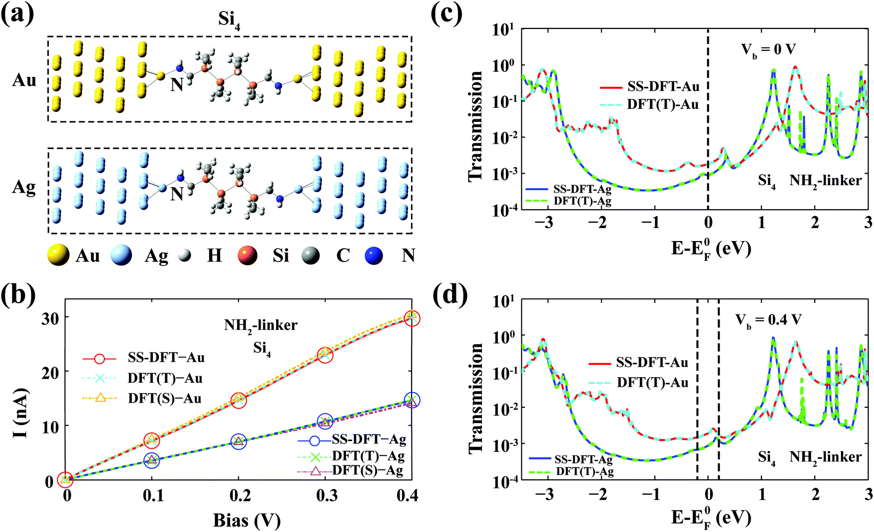 | ||
| Fig. 1 Transport properties of the amine-terminated silane junctions Si4–NH2–M. (a) The optimised atomic structures of Si4–NH2–M (M = Au or Ag). (b) The I–V curves of Si4–NH2–M calculated from SS-DFT and two DFT-based packages, TranSIESTA (DFT(T)) and SMEAGOL (DFT(S)). The three packages agree with each other remarkably well. (c) and (d) Transmission spectra obtained from SS-DFT and TranSIESTA are shown in (c) for Vb = 0 V and in (d) for Vb = 0.4 V. E0F in (c) and (d) denotes the Fermi energy of the junction at zero bias. | ||
It is not surprising that the Au contact provides better conductivity than the Ag contact, which is a natural consequence of the ground-state properties of Au and Ag elements. Although Au and Ag are in the same group of the periodic table and have similar broad s band characteristics, it is known that the density of states (DOS) of Au is pronouncedly higher than that of Ag at EF due to the relativistic effect induced upshift of the d bands.22,23 In Fig. S2 (ESI†), we plotted the ground-state local DOS of the Au and Ag atoms that bind with the silane molecules. The higher DOS of Au at EF (than that of Ag) due to the up-shifted d bands can be clearly seen, which results in the higher conductance of the Au contact when the system is not far from equilibrium.
The thiol-terminated silane junctions Sin–S–M
We consider the Sin–S–M (M = Au, Ag) junctions for n = 3, 6 and 7. Their optimised atomic structures are shown in Fig. 2–c. The corresponding I–V curves for both the Au and Ag contacts obtained from the DFT-based method, via the TranSIESTA and SMEAGOL packages, were plotted in Fig. 2d–f, where we see that both computational packages still predict that the Au contact is more conducting than the Ag contact for all cases with SMEAGOL generating a more significant difference between Au and Ag than TranSIESTA. ATK gives the same prediction as shown in the I–V curves for n = 7 in Fig. S1b (ESI†). The calculations based on the standard DFT method contradict with the experiment, which shows that the Ag contacts provide a much higher conductivity than those of the Au contacts. Another puzzling feature of the I–V curves in Fig. 2 is that, unlike the case of the NH2 linker for which the TranSIESTA and SMEAGOL packages agree with each other amazingly well (Fig. 1b), the two packages yield quantitatively quite different I–V curves despite being built on the same DFT-based transport method and employing the same set of parameters in the calculations (bases, pseudopotentials etc., see the Methods section). The difference between the electric currents from the two packages can be as much as 30% at 0.4 V. On the other hand, the zero-bias conductance calculated from both packages for different cases (Table S1, ESI†) is quite similar with at most around a 2% difference.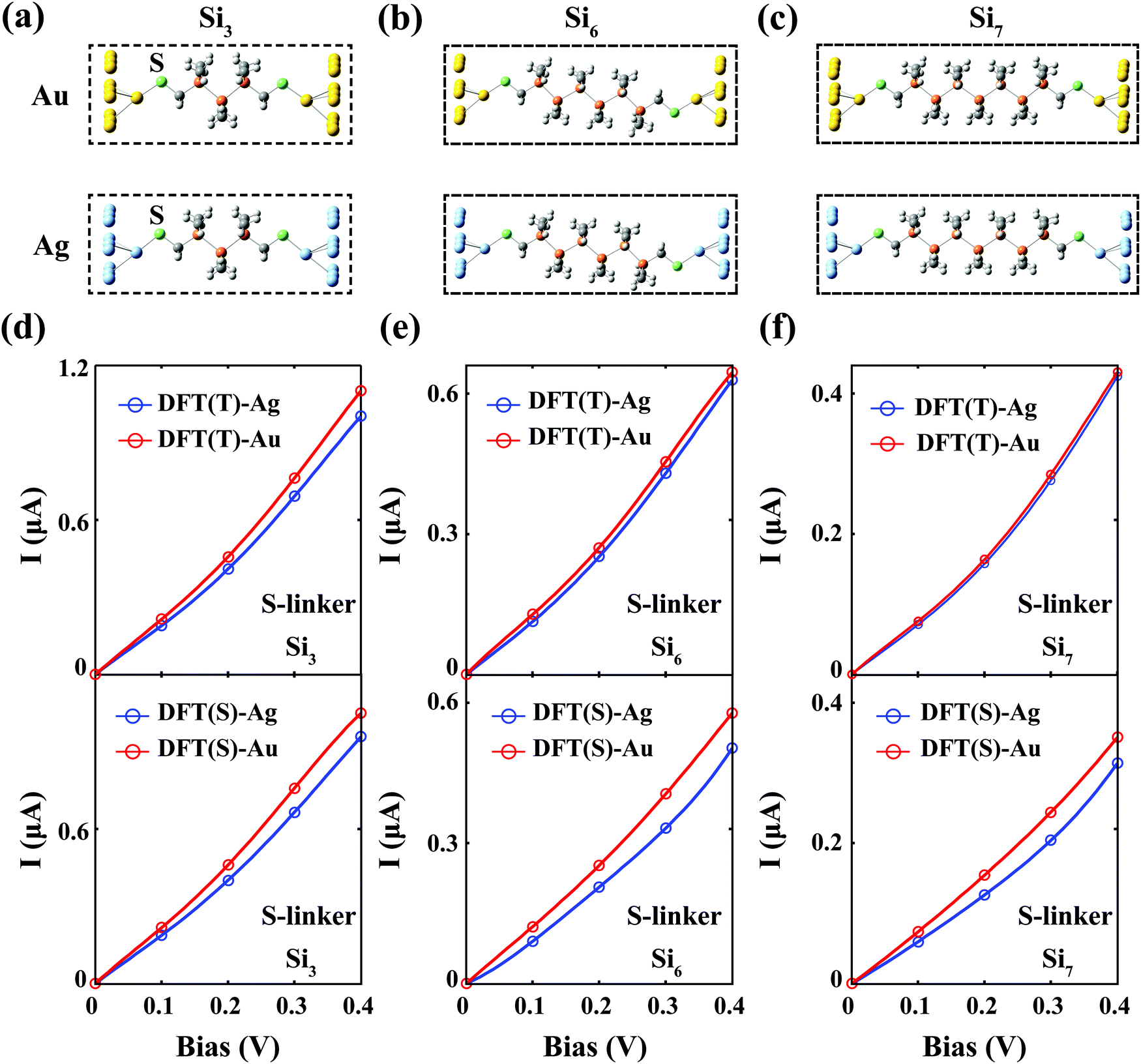 | ||
| Fig. 2 I–V curves of the thiol-terminated silane junctions Sin–S–M calculated from the DFT-based method. (a–c) The optimised atomic structures of Sin–S–M (M = Au or Ag) are shown in (a) for n = 3 (Si3), (b) for n = 6 (Si6) and (c) for n = 7 (Si7). (d–f), I–V curves calculated from two DFT-based packages, TranSIESTA (DFT(T)) and SMEAGOL (DFT(S)), are shown in (d) for n = 3, (e) for n = 6 and (f) for n = 7. DFT(T or S)-Au/Ag denotes TranSIESTA or SMEAGOL results for Sin–S–Au/Ag. For all cases, the Au contact produces a higher conductivity than that of the Ag contact. | ||
The significant quantitative difference in the I–V curves (together with essentially the same equilibrium conductance) produced by the two DFT-based packages is an indication of significant bias-induced nonequilibrium effects in the system. At equilibrium (Vb = 0 V), conventional DFT is applicable, and the properties of the system can be uniquely determined by the total electron density ρt. TranSIESTA and SMEAGOL optimise ρt by the same DFT-based self-consistent process, and therefore shall obtain similar ρt, which in turn guarantees similar equilibrium properties. Under finite Vb, it has been proven that the properties of the system depend on two densities, ρt and ρn, and ρt alone cannot uniquely determine the system.19 Since the DFT method only optimises ρt, the un-optimised ρn from different packages may differ substantially depending on their detailed numerical procedures upon convergence of ρt, resulting in different I–V curves.
To capture the nonequilibrium effects in full, we performed SS-DFT calculations. The I–V curves for Sin–S–M (M = Au, Ag) junctions are shown in Fig. 3a–c for n = 3, 6 and 7, respectively. As a reference, the results from TranSIESTA are also included. For all cases, when the bias is low enough (≤0.1 V), there is essentially no difference between the SS-DFT and DFT-based methods and SS-DFT also predicts that Au provides slightly better conductivity than that of Ag. A significant deviation occurs after 0.1 V, where the electric currents from SS-DFT for the Ag contact start to increase more rapidly than those for Au. For all cases of n, the current of the Ag contact surpasses that of the Au contact at 0.2 V, and when the bias further increases, the difference between the currents of Ag and Au also widens. To better compare with the experiment18 that reported the trend reversal of low-bias conductance (measured at 0.2 V), we plotted the differential conductance at 0.2 V calculated from SS-DFT in Fig. 3d. For comparison, the differential conductance of the junctions Si4–NH2–M (M = Au, Ag) is shown in the inset. We see that according to SS-DFT, for the NH2 linker, the conductance of the Au contact is approximately 2.3 times higher than that of the Ag contact, while for the S linker, the conductance of Ag is about 1.2, 1.4 and 1.5 times higher than that of Au for n = 3, 6 and 7, respectively. Thus, the experimentally observed trend reversal of low-bias conductance is captured in SS-DFT. The differential conductance at 0.2 V from TranSIESTA and SMEAGOL is shown in Fig. S3 (ESI†), where both packages predict that the Au contact provides a higher conductance than that of the Ag contact regardless of the linker.
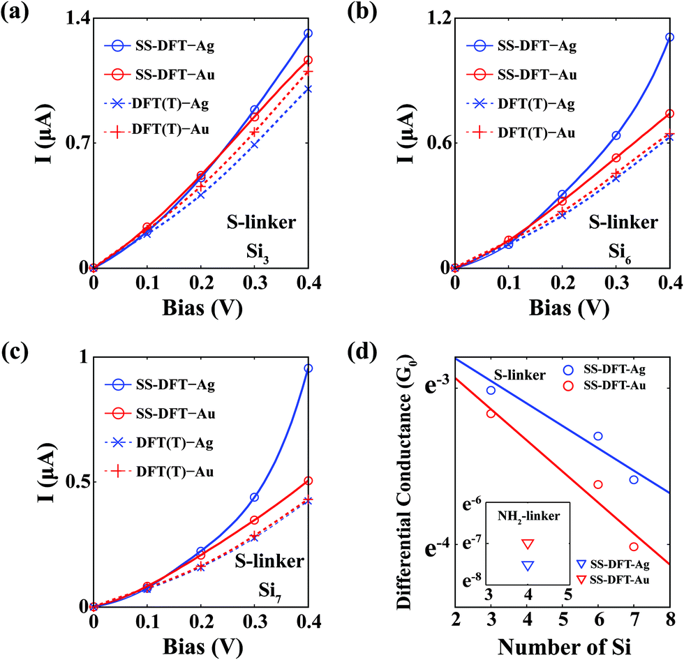 | ||
| Fig. 3 I–V curves of the thiol-terminated silane junctions Sin–S–M calculated from the SS-DFT method. The I–V curves of Sin–S–M calculated from the SS-DFT method are shown in (a) for n = 3 (Si3), (b) for n = 6 (Si6) and (c) for n = 7 (Si7). SSDFT-Au/Ag denotes SS-DFT results for Sin–S–Au/Ag. As a reference, I–V curves from TranSIESTA (DFT(T)) are also shown (dotted lines in the figures). Note that at small biases (≤0.1 V), there are no essential differences between the two methods. Significant differences occur at biases >0.1 V. (d) Differential conductance of Sin–S–M (M = Au or Ag) at 0.2 V calculated from SS-DFT for n = 3, 6 and 7. The two solid lines in the figure are obtained by linear fitting. Inset: differential conductance of Sin–NH2–M (M = Au or Ag) at 0.2 V from SS-DFT. For the NH2 linker, the Au contact is more conducting than the Ag contact. The trend reverses for the S linker. | ||
Prominent effects of the ‘nonequilibrium pulling’
We use the Si7–S–M junction to elucidate the origin of the bias-induced nonequilibrium effects, as similar junctions were theoretically studied before.18 In Fig. 4, we plot the zero-bias transmission spectra of Si7–S–M calculated from both SS-DFT and TranSIESTA. As expected, at zero bias, the two packages yield almost exactly the same transmission function. At EF, the Au contact exhibits a higher conductance than that of the Ag contact, unsurprisingly, which agrees with the previous DFT study.18 Shown in Fig. 4 are two major peaks near the EF of transmission for both the Ag (A and B) and Au (C and D) cases. Comparing the tunnelling eigenstates at those peaks (Fig. 4) with frontier orbitals of SH–Si7 (Fig. S4, ESI†), we see that peaks A and C originated from tunnelling through the HOMO−1 orbitals of SH–Si7 that are mainly localised at the source contact, while peaks B and D come from the HOMO that resides in the centre of the molecule. Peak A is much (nearly 2 times) higher than C, which is caused by the different bonding nature between Ag–S and Au–S. Ag has a lower electronegativity than that of Au, resulting in a greater charge transfer to the S atom from Ag (0.25|e|) than that from Au (0.16|e|) according to Voronoi population analysis.24 The nearly 0.1|e| difference in the two cases originates from the electron transfer from the Ag 4d to the S 3p that is located about 1 eV below EF (see the shaded area in the projected DOS of S in Fig. S5, ESI†), which enhances the coupling between the Ag contact and the S linker around the same energy and in turn leads to the high transmission peak A (see Fig. S5, ESI†). In Fig. 4, the tunnelling eigenstates at EF are also shown, which clearly suggest that the transmission at EF is determined by the tail of the broader HOMO−1 peak rather than the HOMO peak for both the Au and Ag cases.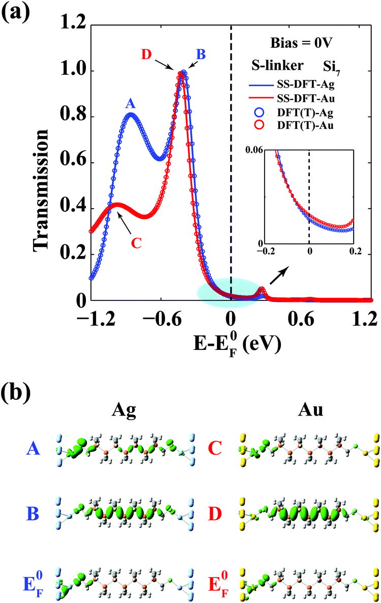 | ||
| Fig. 4 Zero-bias transmission spectra of Si7–S–M. (a) Transmission spectra of Si7–S–M (M = Au, Ag) from SS-DFT and TranSIESTA (DFT(T)). For both the Au and Ag cases, the results from the two packages are essentially the same. Inset: enlarged view of the transmission spectra near the Fermi energy. Note that the Au contact is more conducting than the Ag contact. (b), Tunneling eigenchannels of major peaks in the transmission spectra, A and B for the Ag contact, and C and D for the Au contact. Tunneling eigenchannels at the Fermi energy were also plotted. | ||
The response of the main peaks in the transmission spectra to the bias voltages determines the I–V curves. In Fig. 5, we plotted the transmission spectra of the M–S–Si7 junction at different biases from both SS-DFT and TranSIESTA. The bias window where current-carrying electrons are located is shown in the figure. When a bias is applied, an additional electrostatic potential is established in the device region that leads to a potential drop from the source  to the drain
  . Note that E0F is the Fermi level of the system at zero bias. This additional electrostatic potential, however, has little effect on the energy of the HOMO of the molecule since the orbital resides in the middle and is symmetrically distributed across the molecule. Consequently, for both SS-DFT and DFT, the HOMO peaks (for both the Au and Ag contacts) remain essentially stationary when the bias increases (see Fig. 5a and b). In contrast, the potential of the source,
  , heavily influences the energy of the HOMO−1 orbital, which is localised at the source contact, leading to the upshift of the HOMO−1 peaks when the bias increases as shown in Fig. 5. The HOMO−1 peak of Si7–S–Au in the transmission spectra is much lower than that of Si7–S–Ag and submerges into the much higher HOMO peak as shown in the figure. We therefore focus our discussion on the HOMO−1 peak of Si7–S–Ag. At zero bias, the separation between the HOMO−1 and HOMO peak of Ag–S–Si7 is 0.45 eV (the same for both SS-DFT and TranSIESTA). When the bias increases to 0.2 V, the separation becomes 0.38 eV for TranSIESTA and 0.26 eV for SS-DFT. At 0.4 V, the separation is 0.33 eV and 0.15 eV for TranSIESTA and SS-DFT, respectively. The HOMO−1 peak from SS-DFT moves significantly faster towards the right than that from TranSIESTA, suggesting that besides the bias-induced electrostatic potential, there should exist an additional ‘force’ pulling the peak towards the bias window.
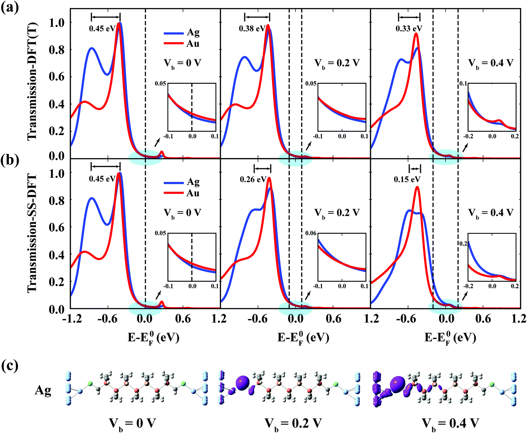 | ||
| Fig. 5 Transmission spectra of Si7–S–M under different biases. (a and b) Transmission spectra of Si7–S–M (M = Au, Ag) at different bias voltages calculated from TranSIESTA (DFT(T)) in (a) and SS-DFT in (b), with the separation between the HOMO−1 and HOMO peaks for the Ag contact shown. Two dotted lines for the non-zero bias cases denote the bias window. SS-DFT predicts a bias-induced ‘nonequilibrium pulling’ that pulls the HOMO−1 peak localised at the source contact towards the bias window. Insets: enlarged view of transmission in the bias window for finite biases and from −0.1 to 0.1 eV for zero bias. (c) Iso-surface of the current-carrying electron density at different biases for the Ag contact calculated from SS-DFT. Note that for zero bias, the current-carrying electron density is zero. At finite biases, the current-carrying density mainly accumulates at the source contact. | ||
The additional ‘pulling force’ originates from the nonequilibrium effects in the process of minimizing Ẽ in eqn (1). The bias-dependent term En[ρn] in eqn (1) can be calculated as 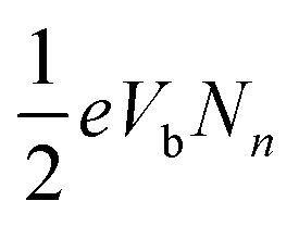 (see Methods section), where Nn is the number of current-carrying electrons. Since the term is always positive, the process of minimizing Ẽ tends to pull the orbital outside the bias window towards the window to increase Nn and En, which ultimately decreases Ẽ. On the other hand, this nonequilibrium effect induced ‘pulling’ (which we name ‘nonequilibrium pulling’ in this paper) also tends to increase the energy of the steady state, ESS, by causing a further upshift of the HOMO and HOMO−1 peaks in the energy axis. The minimizing process of Ẽ in SS-DFT is therefore a competition between these two energies, ESS and En. The current-carrying electron density, ρn, mainly accumulates around the source contact (Fig. 5c) where the reflection of current-carrying electrons takes place. The nonequilibrium effects therefore are most significant for the states localised at the source contact, which is the reason why we see clear ‘pulling’ of the HOMO−1 peaks towards the bias window from SS-DFT in Fig. 5b. For HOMO peaks residing in the molecular centre, however, the nonequilibrium effects are much weaker, and the ‘pulling’ induced increase of En cannot compensate for the increase of ESS, thus the pulling is trivial. It is the nonequilibrium pulling of the HOMO−1 peak of Si7–S–M that significantly enhances the transmission in the bias window at 0.2 and 0.4 V (as can be seen in the insets of Fig. 5a and b), leading to the trend reversal of differential conductance discussed earlier.
To see the difference between the SS-DFT and the DFT-based methods more clearly, we show schematically the searching paths of the two methods for the transport state in Fig. 6a. The steady-state energy, ESS[ρt, ρn], is represented by a two-dimensional (2d) colour contour map. SS-DFT searches for the minimum of Ẽ[ρt,ρn] (instead of ESS) in the 2d plane and shall end up with a state near the minimum of ESS, while the DFT-based method searches for the stable transport state along the ρt axis. The extent of the 2d SS-DFT searching along the ρn axis, δρn, can be measured by the number of current-carrying electrons in the molecular centre, Nn, which can be calculated by the integral of ρn in the centre. When Nn is small (not far from equilibrium), the SS-DFT searching trajectory is close to the ρt axis as shown in Fig. 6a, therefore yielding similar results to that of DFT. The Si4–NH2–M and the Si7–S–M junctions at small biases (≤0.1 V) belong to this category (see Fig. 6b). When Nn is significant, SS-DFT finds the stable steady state far away from equilibrium in the 2d plane, which is the case for Si7–S–M at biases ≥ 0.2 V (Fig. 6b).
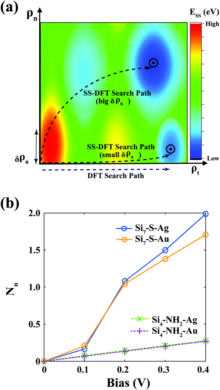 | ||
| Fig. 6 Conceptual differences between the SS-DFT and DFT-based methods. (a) A schematic plot of the different searching paths of the SS-DFT and the DFT-based methods. The 2d color contour represents the steady-state energy in SS-DFT, Ess, which is a functional of two densities, ρn and ρt. The SS-DFT searches for the transport state with minimum effective energy Ẽ in the 2d plane that shall be located around the minimum Ess. The DFT method searches the most stable transport state along the axis of total electron density ρt. When δρn is small, the searching path of SS-DFT is close to the ρt axis, which generates similar results to the DFT method. (b) The number of current-carrying electrons in the molecular centre, Nn, for Si7–S–M and Si4–NH2–M (M = Au or Ag) at different bias voltages. | ||
Conclusions
In summary, with both the DFT-based approach and the SS-DFT method, we studied the transport properties of the amine- and thiol-terminated silanes with Au and Ag contacts. We found that all three prevalent implementations of the DFT-based approach qualitatively agree with each other and predict that the Au contact is always more conducting than the Ag contact regardless of the linker. In contrast, while the SS-DFT agrees with the standard DFT method for the amine-terminated silane junctions, it predicts a striking trend reversal of low-bias conductance in thiol-terminated silane junctions that the Ag contact yields a significantly higher conductance than that of the Au contact, which is consistent with experimental observations. Detailed analysis suggests that a novel type of nonequilibrium effect, referred to as “nonequilibrium pulling” in this work, in which the conducting channels mainly reside on the source contact and are pulled towards the bias window, plays an essential role in the observed conductance trend reversal. Further analysis indicates that when the device is near equilibrium, the DFT-based approach is an excellent approximation of SS-DFT, but when there are conducting channels at the source contact that are close to the bias window, ‘nonequilibrium pulling’ could generally exist, causing the failure of the standard DFT approach, and then SS-DFT becomes necessary in modelling the device. These findings significantly broaden our understanding of electron transport at the nanoscale and provide guidelines for future computational studies of nanoscale devices.Methods
Computational details
Structure optimizations of all junctions were done using the SIESTA25 and transport calculations were performed with the SS-DFT,19 TranSIESTA,16 SMEAGOL,17 and ATK-201320 packages. In all calculations, the generalised gradient approximation (GGA) in PBE format,26 double-ζ polarised basis and 4 × 4 × 4 k-point sampling in the Brillouin zone for bulk materials were employed. A 4 × 4 × 1 k-point sampling in the device region was adopted in the transport calculations. While ATK uses its own built-in pseudopotentials, all other computational packages use the norm-conserving pseudopotentials in the Troullier–Martins scheme27 with the same set of parameters.28 Scalar-relativistic effects were considered for Au and Ag. Nonequilibrium corrections to the exchange functional in an analytic form29,30 were included in the SS-DFT calculations. Energy and force convergence criteria were set to 10−4 eV and 0.03 eV Å−1, respectively.To test the validity of the parameters used, we compare the band structures of the Au/Ag bulk and the HOMO–LUMO gaps of silanes calculated from SIESTA with those from VASP.31 VASP calculations were employed a plane-wave basis set with a 450 eV energy cut-off, the PAW pseudopotentials32 and GGA in PBE format. The results are shown in Fig. S8 and Table S2 in the ESI,† where we can see that SIESTA and VASP gave almost exactly the same band structures for the Au and Ag bulk and quite similar HOMO–LUMO gaps for the silanes. It is worth mentioning here that the accuracy of the DFT-calculated energy level alignment of molecular states with the Fermi level of a metal substrate can be significantly improved using the DFT + ∑ approach.33
Energies in SS-DFT
The central physical quantity in SS-DFT is the effective energy, Ẽ[ρt,ρn], that is a functional of ρt and ρn, and can be calculated by subtracting the bias-dependent nonequilibrium energy, En[ρn] , from the energy of the steady state, ESS[ρt,ρn], as shown in eqn (1). The integral,
  can be interpreted as the number of current-carrying electrons, Nn. The steady-state energy functional ESS[ρt,ρn] is defined in the following equation,
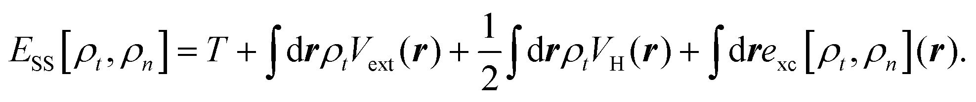 | (2) |
Data availability
All data supporting the findings of this study are available within the article and its ESI,† or from the corresponding author upon reasonable request.Author contributions
CZ conceived the project. ZJ and KY did most calculations. KY and CZ wrote the paper. All authors contributed to data analysis and finalization of the paper.Conflicts of interest
The authors declare no competing interests.Acknowledgements
We acknowledge the support from the Ministry of Education of Singapore (R-723-000-029-112), the NUS academic research fund (R-144-000-410-114; R-265-000-691-114) and the NUS green energy program (R-143-000-A63-114). Computational works were performed at the NUS Graphene Research Centre computing cluster facilities.References
- A. W. Ghosh, T. Rakshit and S. Datta, Nano Lett., 2004, 4, 565–568 CrossRef CAS.
- H. Song, Y. Kim, Y. H. Jang, H. Jeong, M. A. Reed and T. Lee, Nature, 2019, 462, 1039–1043 CrossRef.
- C. Zhang, M. Du, H.-P. Cheng, X.-G. Zhang, A. E. Roitberg and J. L. Krause, Phys. Rev. Lett., 2014, 92, 158301 CrossRef.
- M. del Valle, R. Gutiérrez, C. Tejedor and G. Cuniberti, Nat. Nanotechnol., 2007, 2, 176–179 CrossRef CAS PubMed.
- C. Jia, A. Migliore, N. Xin, S. Huang, J. Wang, Q. Yang, S. Wang, H. Chen, D. Wang, B. Feng, Z. Liu, G. Zhang, D.-H. Qu, H. Tian, M. A. Ratner, H. Q. Xu, A. Nitzan and X. Guo, Science, 2016, 352, 1443–1445 CrossRef CAS PubMed.
- K. Stokbro, J. Taylor and M. Brandbyge, J. Am. Chem. Soc., 2003, 125, 3674–3675 CrossRef CAS PubMed.
- Y. Q. Cai, A. H. Zhang, Y. P. Feng and C. Zhang, J. Chem. Phys., 2011, 135, 184703 CrossRef PubMed.
- A. Batra, P. Darancet, Q. Chen, J. S. Meisner, J. R. Widawsky, J. B. Neaton, C. Nuckoll and L. Venkataraman, Nano Lett., 2013, 13, 6233–6237 CrossRef CAS PubMed.
- C. Zhang, X.-G. Zhang, P. S. Krstic, H.-P. Cheng, W. H. Butler and J. M. Maclaren, Phys. Rev. B: Condens. Matter Mater. Phys., 2004, 69, 134406 CrossRef.
- Z. Y. Lu, X. G. Zhang and S. T. Pantelides, Phys. Rev. Lett., 2005, 94, 207210 CrossRef PubMed.
- S. Barazza-Lopez, K. Park, V. García-Suárez and J. Ferrer, Phys. Rev. Lett., 2009, 102, 246801 CrossRef PubMed.
- A. Nitzan and M. A. Ratner, Science, 2003, 300, 1384–1389 CrossRef CAS.
- J. R. Heath and M. A. Ratner, Phys. Today, 2003, 56, 43–49 CrossRef CAS.
- L. Venkataraman, J. E. Klare, C. Nuckolls, M. S. Hybertsen and M. Steigerwald, Nature, 2006, 442, 904–907 CrossRef CAS PubMed.
- J. Taylor, H. Guo and J. Wang, Phys. Rev. B: Condens. Matter Mater. Phys., 2001, 63, 121104 CrossRef.
- M. Brandbyge, J. L. Mozos, P. Ordejón, J. Taylor and K. Stokbro, Phys. Rev. B: Condens. Matter Mater. Phys., 2002, 65, 165401 CrossRef.
- A. R. Rocha, V. García-Suárez, S. W. Bailey, C. J. Lambert, J. Ferrer and S. Sanvito, Nat. Mater., 2005, 4, 335–339 CrossRef CAS.
- H. Li, T. A. Su, M. Camarasa-Gómez, D. Hernangómez-Pérez, S. E. Henn, V. Pokorný, C. D. Caniglia, M. S. Inkpen, R. Korytár, M. L. Steigerwald, C. Nuckolls, F. Evers and L. Venkataraman, Angew. Chem., Int. Ed., 2017, 56, 14145 CrossRef CAS PubMed.
- S. Liu, A. Nurbawono and C. Zhang, Sci. Rep., 2015, 5, 15386 CrossRef CAS.
- S. Smidstrup, T. Markussen, P. Vancraeyveld, J. Wellendorff, J. Schneider, T. Gunst, B. Verstichel, D. Stradi, P. A. Khomyakov, U. G. Vej-Hansen, M.-E. Lee, S. T. Chill, F. Rasmussen, G. Penazzi, F. Corsetti, A. Ojanpera, K. Jensen, M. L. N. Palsgaard, U. Martinez, A. Blom, M. Brandbyge and K. Stokbro, J. Phys.: Condens. Matter, 2020, 32, 015901 CrossRef CAS PubMed.
- S. Hershfield, Phys. Rev. Lett., 1993, 70, 2134 CrossRef CAS.
- O. Jepsen, D. Glötzel and A. R. Mackintosh, Phys. Rev. B: Condens. Matter Mater. Phys., 1981, 23, 2684–2696 CrossRef CAS.
- O. Adak, R. Korytár, A. Y. Joe, F. Evers and L. Venkataraman, Nano Lett., 2015, 15, 3716–3722 CrossRef CAS.
- C. Fonseca Guerra, J.-W. Handgraaf, E. J. Baerends and F. M. Bickelhaupt, J. Comput. Chem., 2004, 25, 189–210 CrossRef PubMed.
- J. M. Soler, E. Artacho, J. D. Gale, A. García, J. Junquera, P. Ordejón and D. Sánchez-Portal, J. Phys.: Condens. Matter, 2002, 14, 2745–2779 CrossRef CAS.
- J. P. Perdew, K. Burke and M. Ernzerhof, Phys. Rev. Lett., 1996, 77, 3865 CrossRef CAS.
- N. Troullier and J. L. Martins, Phys. Rev. B: Condens. Matter Mater. Phys., 1991, 43, 1993 CrossRef CAS PubMed.
- S. García-Gil, A. García, N. Lorente and P. Ordejón, Phys. Rev. B: Condens. Matter Mater. Phys., 2009, 79, 075441 CrossRef.
- S. Liu, Y. P. Feng and C. Zhang, J. Chem. Phys., 2013, 139, 191103 CrossRef PubMed.
- C. Zhang, J. Atom. Mol. Sci., 2013, 5, 95–99 Search PubMed.
- G. Kresse and J. Furthmüller, Phys. Rev. B: Condens. Matter Mater. Phys., 1996, 54, 11169 CrossRef CAS PubMed.
- P. E. Blöchl, Phys. Rev. B: Condens. Matter Mater. Phys., 1994, 50, 17953 CrossRef.
- D. A. Egger, Z. Liu, J. B. Neaton and L. Kronik, Nano Lett., 2015, 15, 2448–2455 CrossRef CAS PubMed.
Footnotes |
| † Electronic supplementary information (ESI) available: Fig. S1–S6, and Tables S1–S2. See DOI: 10.1039/d1nh00293g |
| ‡ These authors contributed equally. |
| This journal is © The Royal Society of Chemistry 2021 |