
 Open Access Article
 This Open Access Article is licensed under a Creative Commons Attribution-Non Commercial 3.0 Unported Licence
Gold nanoplasmonic particles in tunable porous silicon 3D scaffolds for ultra-low concentration detection by SERS†
Rihan
Wu‡
a,
Qihao
Jin‡
 b,
Catherine
Storey
a,
Jack
Collins
a,
Guillaume
Gomard
c,
Uli
Lemmer
b,
Leigh
Canham
a,
Rainer
Kling
b and
Andrey
Kaplan
*a
b,
Catherine
Storey
a,
Jack
Collins
a,
Guillaume
Gomard
c,
Uli
Lemmer
b,
Leigh
Canham
a,
Rainer
Kling
b and
Andrey
Kaplan
*a
aSchool of Physics and Astronomy, University of Birmingham, Birmingham B15 2TT, UK. E-mail: a.kaplan.1@bham.ac.uk
bLight Technology Institute, Karlsruhe Institute of Technology, Engesserstrasse 13, 76131 Karlsruhe, Germany
cCarl Zeiss AG, ZEISS Innovation Hub@KIT, Hermann-von-Helmholtz-Platz 6, 76344 Eggenstein-Leopoldshafen, Germany
First published on 16th July 2021
Abstract
A composite material of plasmonic nanoparticles embedded in a scaffold of nano-porous silicon offers unmatched capabilities for use as a SERS substrate. The marriage of these components presents an exclusive combination of tightly focused amplification of Localised Surface Plasmon (LSP) fields inside the material with an extremely high surface-to-volume ratio. This provides favourable conditions for a single molecule or extremely low concentration detection by SERS. In this work the advantage of the composite is demonstrated by SERS detection of Methylene Blue at a concentration as low as a few picomolars. We systematically investigate the plasmonic properties of the material by imaging its morphology, establishing its composition and the effect on the LSP resonance optical spectra.
New conceptsWe developed a new substrate for on-chip Surface Enhanced Raman Spectroscopy. The substrate surpasses known alternatives and provides signal enhancement by a factor of 109, achieving a single-molecule detection level. This property has been corroborated by detecting Raman scattering from an analyte with picomolar (10−12 M) concentration of methylene blue dye. To achieve the break-through quality, we developed a new method to embed gold nanoclusters into a 3D scaffolding of nano-porous silicon (npSi). This new composite material combines unique properties of both components. The role of gold nanoclusters is to enhance the light field by means of Localised Surface Plasmon (LSP) resonance excitation. The function of the npSi dielectric environment is to tighten further the localisation and provide an enormous area exposed to LSP. Thus, analyte molecules adsorbed on the pores have an exceedingly high chance to interact with the tightly-focused LSP and participate in enhanced Raman scattering. The material applications spread far beyond SERS because it combines the rich world of nanoplasmonics with the high-tech of semiconductors. Plasmonics materials have excellent absorption cross-section, high electron concentration and tunability, the properties sought to enhance the performance of semiconductor detectors, lasers and imaging sensors. We are hopeful that our development will advance significantly the implementation of plasmonic/semiconductor composites into industrial applications. |
Localised Surface Plasmon (LSP) is a coherent oscillation of electrons at the interface between metallic nanoparticles and the surrounding medium. LSP can be excited by light when its frequency matches that of the oscillations, producing a strong enhancement of the electromagnetic field in the vicinity of the particles under the conditions of the resonance.1 The LSP Resonance (LSPR) is distinguished by intense absorption and scattering of light. Its wavelength and intensity are primarily determined by the type of material, size, shape, environment refractive index and coupling between adjacent nanoparticles.2–4 In the past few decades, extensive studies have been conducted to adopt LSPR in biological and chemical sensing systems due to its high sensitivity to the surrounding environment.5,6 The ability of photon-trapping and strong absorption of LSPR at the resonance wavelength have further promoted its implementation in light harvesting devices.7,8 Other fields of research and applications extend to metamaterials,9 plasmonic devices,10,11 diagnosis and treatment of diseases.12–14
Several types of LSPR substrates with nanoparticles in colloidal suspension, deposited on the surface and embedded in a dielectric matrix have been developed and investigated.15–17 The former two types are most commonly used in biological and chemical sensing systems, implementing Surface Enhanced Raman Spectroscopy (SERS), where the analytes are either mixed with colloidal solution or in contact with the substrate surface.18 The LSPR induced by nanoparticles localises and enhances the electromagnetic field which amplifies the Raman signal of the surrounding molecules.19 In the latter type, metallic nanoparticles are usually embedded into a nonconducting solid state environment, such as silicon oxide or organic polymers.20 These hybrid composite materials not only preserve the LSPR response of the metal nanoparticles from degradation, but also improve the robustness and responsiveness, thereby further expanding their application range. The use of plasmonic nanoparticles was extended to Au@Pt core–shell nanostructures facilitating dual functionalities to track Pt-catalysed reactions and quantitatively analyse the response by SERS. The particles preserve their morphological uniformity as revealed by TEM imaging after a few cycles of recycling following the particles’ use in a catalytic reaction.21 Although there are many advantages of hybrid bulk composites over solution/surface counterparts, technological limitations to embed metallic nanoparticles into the matrix of bulk materials, in particular semiconductors, remain unresolved, because of difficulties involved in the fabrication process. The conventional mixing methods, such as melt quenching,22 colloidal method23 and metal-dielectric co-sputtering,24 are either not suitable or have not been developed to an adequate level suitable for the large-scale and low-cost fabrication of nanoplasmonic–semiconductor composites. Nevertheless, recent studies have revealed fascinating properties and perspectives of nanoplasmonic–semiconductor composites for enhanced efficiency of photocatalysis,25,26 as well as demonstration of a mechanism of plasmon-induced hot carrier generation and their migration through a Schottky barrier of Au/TiO dumbbell structures, enhancing the photocatalytic performance.27 Other examples of the composites’ applications include amplifications of photoluminescence,28 solar energy conversion29 and optical nonlinearities.30
In this work, we aim to develop a method scalable for the production of large quantities of nanoplasmonic–semiconductor composites exhibiting high uniformity. Nano-porous silicon (np-Si) was selected as the semiconductor matrix due to its low manufacturing cost,31 robustly developed fabrication process and in-depth documented optical and electronic properties.32,33 Moreover, np-Si provides a natural template for metallic nanoparticle growth inside the interconnected nano-sized pore channels. We developed a method of spontaneous growth of Au nanoparticles (AuNPs) inside np-Si using the immersion plating technique. This process demands precise control of the solution temperature and concentration to ensure uniform growth of Au particles inside the pores, while concurrently minimising unwanted particle clustering on the np-Si facets. We fabricated samples with different volume fractions of Au nanoparticles and examined their composition, morphology and uniformity by means of Scanning Electron Microscopy (SEM) and Transmission Electron Microscopy (TEM). We show that the nanoparticle size and density distribution can be controlled by varying the deposition time and solution concentration. The presence of the LSPR was observed by dark-field microscope and a VIS-NIR scattering spectrometer. Au/np-Si composites exhibit the LSPR at the red end of the visible spectrum, extending to the near infrared region for the samples with increasing Au nanoparticle volume fractions.
The sample with the highest Au volume fraction was used as a SERS substrate to measure the Raman spectrum of the Methylene Blue (MB) benchmark compound. We demonstrate an enhancement factor of ∼109 under the excitation wavelength of 808 nm in the vicinity of the LSPR. Such enhancement is suitable for a scenario where a single molecule detection is desired.34,35
1 Results and discussion
Sample preparation and characterisation
We adopted a wet chemical synthesis method based on the previously reported studies36,37 exploring gold ion reduction from a solution of tetrachloroauric acid (HAuCl4) with borohydride as a reducing agent. However, in this work, we adopted a procedure where no reducing agent was required. Instead, hydrogen atoms chemisorbed at the pore surface of np-Si act as a reducing agent during AuNP impregnation (see Methods). Fig. 1(a) wrap-ups the main steps of the sample preparation. A 550 nm-thick np-Si layer with underlaying silicon substrate was pre-treated with 2% HF solution for 30 s to remove the native oxide from the pore surface and to saturate dangling bonds with hydrogen. After the treatment, the samples were immediately immersed in HAuCl4–ethanol solution, where the gold ion reduction occurs at the pore channel surfaces accompanied by aggregation and spontaneous growth of AuNPs. To facilitate the penetration of the solution into the pores, an ultrasonic bath was used during immersion, which not only enhances the inflow, but also prevents the growth and clustering on the top surface. In addition, the solution concentration and environment temperature play important roles in achieving uniform Au deposition along the depth coordinate. Due to a slow diffusion rate of the solution in np-Si (∼10−9–10−10 m2 s−1),31 AuNPs tend to grow in the direction from the top to the bottom of the substrate. Therefore, controlling the reduction rate through concentration and temperature is essential to ensure the solution reaches the bottom before AuNP grow at the top, blocking the opening of the pore channel. Through iterative experimentation, it was found that at room temperature, the diffusion and reduction rates are balanced for HAuCl4 concentration not greater than 1 mM. At above room temperature the clusters tend to grow on the surface restricting penetration of the solution into the pores and inhibiting uniform growth through the layer thickness. Consequently, we attempted to lower the temperature and increase the flow rate. However, this did not produce reproducible results as it was difficult to maintain the parameters steady without further elaborate development of the set-up. Therefore, we focused on finding a range of concentrations suitable for the impregnation at room temperature. Samples with different densities and sizes of AuNPs were obtained by varying the HAuCl4 concentration and retention time of np-Si in the solution. Table 1 shows the details of the concentration and immersion time of the four samples that were further investigated in this work. The quoted AuNP volume fractions were estimated by modelling the results obtained from angle resolved reflectance measurements (see the ESI†). After the immersion plating, the samples were rinsed in pure ethanol and gently air dried on a hotplate at 60 °C.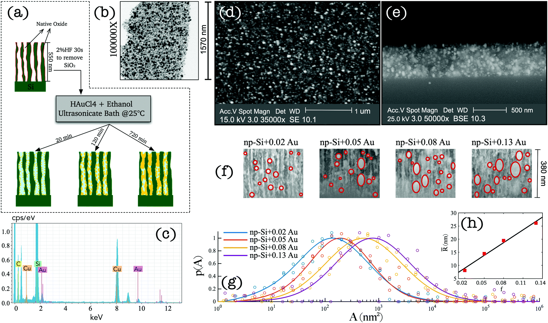 | ||
Fig. 1 (a) Schematical presentation of the fabrication procedure of the Au/np-Si composite material; (b) TEM image of a fragment of Au/np-Si; the dark spots are AuNPs and the bright area is np-Si; (c) EDX spectrum of the Au/np-Si composite; (d) top and (e) cross-section views of the SEM image of the Au/np-Si composite with Au volume fraction of 0.02; (f) zoomed-in cross-section of SEM images for samples with different Au volume fraction, f; (g) scaled probability distribution of cross-sectional area A; (h) ellipsoidal quadratic mean radius, ![[R with combining macron]](https://www.rsc.org/images/entities/i_char_0052_0304.gif) , as a function of AuNP volume fraction, f. , as a function of AuNP volume fraction, f. | ||
| Sample | c (mM) | t (min) | f |
|---|---|---|---|
| Au/np-Si 1 | 0.5 | 10 | 0.02 |
| Au/np-Si 2 | 1 | 20 | 0.05 |
| Au/np-Si 3 | 1 | 120 | 0.08 |
| Au/np-Si 4 | 1 | 720 | 0.13 |
A layer of processed np-Si was gently fractured into small fragments to examine under TEM and Energy-Dispersive X-ray (EDX) to verify the presence of AuNPs. Fig. 1(b) shows the TEM image of an arbitrary segment of the composite. The dark spots are the AuNPs surrounded by the bright sponge of the np-Si matrix. It can be seen that some of the pores are fully occupied by Au, while others remain hollow. Fig. 1(c) shows the EDX spectrum of np-Si after the Au impregnation. The pronounced Au and silicon peaks are clearly observed at their characteristic energies of 2.12, 9.71 and 1.74 eV, respectively.38,39 We note that the carbon and copper peaks are contributed by the supporting TEM grid.
To demonstrate the uniformity of the cluster distribution along the sample depth, we show the top-view and cross-section SEM images of the Au/np-Si composite with a Au volume fraction of 0.02 in Fig. 1(d and e), respectively. These results confirm that there is no aggregation of particles on the top surface, while they are evenly spread along the depth of the 550 nm-thick np-Si matrix. Fig. 1(f) shows the zoomed-in view of the SEM cross-sections for four samples with different AuNP volume fractions, f. It can be seen that the size of the AuNPs increases with the immersion time, while at the longer immersion times the larger clusters tend to grow anisotropically along channels and form rather elliptical shapes. This preferential direction of the growth is imposed by the pore channels walls. By analysing a large number of SEM cross-section images, we obtained the AuNP cluster cross-sectional area distribution as shown in Fig. 1(g). In addition, the ellipsoidal quadratic mean radius, , as a function of Au volume fraction, f, is shown in Fig. 1(h). These figures indicate a general correlation for the clusters to grow larger as their density increases.
Localised surface plasmon resonance
To gain further insight into the nature of Au/np-Si composites, we assessed their optical properties. The samples were imaged by using a real-colour CCD camera through a Dark Field Microscope (DFM) collecting the scattered light. The images are shown in Fig. 2(a–d) where the apparent colour of the scattered light is red. This is in contrast to the typical green colour for similar size AuNPs in air.40 This redshift is attributed to the renormalisation of the LSPR wavelength according to the Fröhlich resonance condition41 for which the Drude dielectric function of gold nanoparticles, εAuNP, matches that of the environment according to εAuNP = −2εenv. For particles in np-Si, the surrounding effective dielectric function, εenv, is nearly twice larger than that of air, resulting in the resonance conditions rearranged towards longer wavelengths.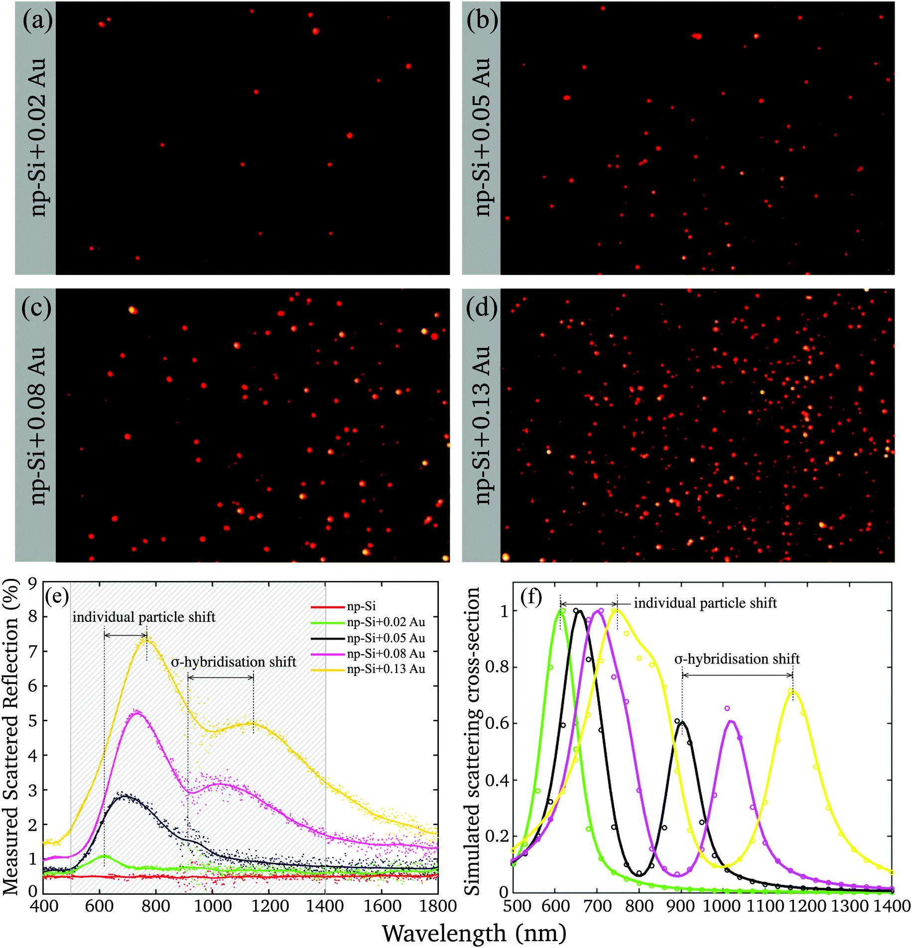 | ||
| Fig. 2 (a–d) Dark Field Microscope (DFM) images of the four samples with different Au volume fractions; (e) measured scattered reflection of np-Si samples without and with different volume fraction of Au; (f) simulated scattering cross-section (normalised) for the fitting parameters listed in Table 2. | ||
Yet, the DFM observation of the scattering has a few limitations. The CCD camera imposes the cut-off wavelength of 650 nm and integrates the spectrum while missing the image of the particles scattering at the longer wavelength. The DFM imaging also tends to grossly overrepresent the high-end tail of the physical cross-section distribution (Fig. 1(g)), while uncounting for the clusters with the dimensions smaller than the microscope resolution limit.
The deficiency was resolved by means of the wavelength-resolved light scattering measurement over an extended VIS-NIR spectral range (see Methods). Fig. 2(e) shows the scattering spectra of np-Si without and with different volume fractions of Au. The scattering spectrum of the np-Si sample without AuNPs is almost flat as its roughness parameter, governed by the pore dimensions, is much smaller than the wavelengths of the spectrum and there are no available scattering centres able to deflect the incoming photons from the original path. However, adding just a minute Au volume fraction of 0.02 to the np-Si results in the appearance of the scattering band peaked around 600 nm, attributed to the LSPR. As the Au volume fraction increases, the resonance peak further shifts to the NIR region, accompanied by the development of the second scattering band, covering the wavelength region between 1000 and 1300 nm. There are two main physical effects that are likely involved in the alteration of the spectrum by increasing the Au fraction in the material.
First, the plasmon resonance shifts towards longer wavelength as the AuNP size increases.42 This is very likely attributed to the change in the local environment surrounding individual particles. While a particle grows, it fills the available space expanding simultaneously towards the opposite wall and along the channel. Hence, the size of a particle determines the fractions of silicon and air in its surrounding. The smaller and round particles are more exposed to air and less to silicon at the interface of the contact area between the pore wall and gold. For larger particles the contact area with silicon increases because of their elliptical shape filling the channel. Hence, the larger particles are locally surrounded by the environment with a higher effective dielectric function and their LSPR wavelength shifts to red with respect to the smaller ones.
Second, the plasmon coupling between adjacent AuNPs can cause the split of the plasmon mode.43,44 Using the AuNPs density and mean radius, it can be estimated that for the lowest fraction, the mean spacing between adjacent AuNPs is relatively large, >10 nm (Fig. S3, ESI†). Thus, for smaller particles and lower densities the interaction is diminishing, because the plasmon field decays over the factor of 1/e within the distance of <5 nm.45 Under these conditions the AuNPs can be treated as isolated clusters surrounded by an np-Si environment. However, at the greater Au volume fractions, which yield larger particles, the spacing between particles is smaller than the field extension and the coupling effect can no longer be ignored. At the larger AuNP densities, the coupling produces an additional plasmon resonance corresponding to the σ-hybridisation of two individual AuNP particles with collinear and unidirectional fields.43 This mode energy is lower than that of a single particle, because of the attractive nature of plasmon–plasmon interaction and it appears in the spectrum at longer wavelength than that of an individual particle. Since the AuNPs in the matrix have rather distributed sizes and spacings, their scattering spectra are composed of weighted contributions from single and hybridised plasmon modes.
We note here that, although the spectra demonstrate a red shift as Au volume fraction increases, the clusters colour remains almost unchanged in the DFM images (Fig. 2(a–d)), because the cut-off wavelength and integration smear the effect.
To gain a quantitative understanding of the observed LSPR spectra, we used the finite element method to simulate the scattering spectra of AuNPs embedded in an np-Si environment (see Methods). The simulation takes as an input of the mean radius, , and spacing, ![[d with combining macron]](https://www.rsc.org/images/entities/i_char_0064_0304.gif) , between gold particles surrounded by np-Si. and were determined from the SEM images, as outlined above. The dielectric function of gold was used from the literature.46 The effective dielectric function of the np-Si environment (without Au inclusions), εenv, was estimated by the use of the Bruggeman model:47,48
, between gold particles surrounded by np-Si. and were determined from the SEM images, as outlined above. The dielectric function of gold was used from the literature.46 The effective dielectric function of the np-Si environment (without Au inclusions), εenv, was estimated by the use of the Bruggeman model:47,48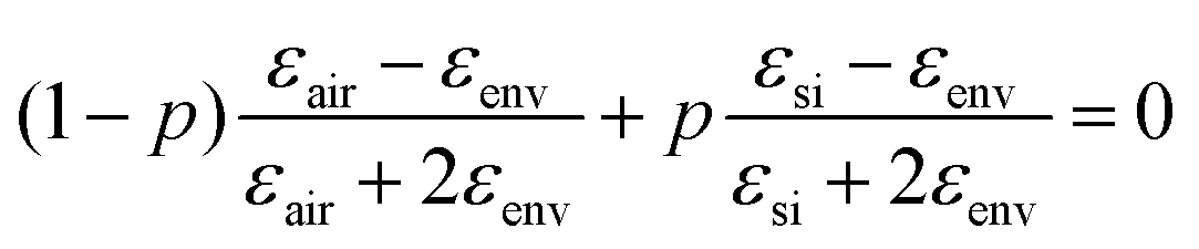 , where p is the volume fraction of silicon and εair = 1. p is an adjustable parameter, which accounts for the fact that εenv depends on the size of gold particles in the pore channel, as discussed previously.
Three main assumptions were made for the simulation: (1) AuNPs are surrounded by a homogeneous environment with the dielectric function of εenv, according to the effective media approximation with adjustable parameter, p; (2) the refractive index of AuNP is the same as that of bulk Au; (3) AuNPs have a spherical shape. Although, the actual shape of the particles is that of a spheroid, they are predominantly oriented with their major axis along the channels and depth coordinate. Hence, at the normal light incidence, light is polarised in the plane of the circular cross-section containing the minor axis.
The simulation results of the normalised scattering cross-section are shown in Fig. 2(f) and the corresponding parameters of the calculations are listed in Table 2. It can be seen that the modelling essentially reproduces the spectral locations of the single particle and σ-hybridisation resonances, as well as the tendency of the former to dominate. The simulation does not include sources of the possible resonance broadening, such as AuNP size and space distribution, deviation from the perfect spherical shape, dependence of the resonance life time on the particle size and contribution from the multipole interactions. Yet, it supports our assumption that the shift of the higher energy resonance (single particle) is proportional to the dielectric function of the effective np-Si environment. While the lower energy resonance depends on the strength of the coupling of an attractive dipole–dipole interaction as d−3.
| Parameter | np-Si + 0.02Au | np-Si + 0.05Au | np-Si + 0.08Au | np-Si + 0.13Au |
|---|---|---|---|---|
| Radius, (nm) |
8.1 | 14.5 | 19.5 | 26.1 |
| Number density, n (m−3) | 9 × 10²¹ | 4 × 10²¹ | 2.6 × 10²¹ | 1.7 × 10²¹ |
| Effective silicon fraction, p | 0.4 | 0.5 | 0.55 | 0.65 |
| Environment permittivity@800 nm | 3.6 + 0.007i | 4.5 + 0.011i | 5.7 + 0.014i | 7.4 + 0.020i |
| Spacing, (nm) |
>10 | 1.3 | 1.25 | 1.05 |
The scattering cross-section, Csca, can be estimated from the measurements of the fractional scattering intensity and compared to the simulation. Isca, the following:49Csca = −ln(Isca)/nh, where n and h are the number of particles per unit volume and thickness of the layer with the embedded scatters. For example, Csca for np-Si + 0.05 Au (n = 4 × 10²¹ m−3, h = 550 × 10−9 m and Isca = 0.05) at 700 nm is about 1.4 × 10⁻¹⁵ m2. The Comsol simulation suggests that embedded Au particles have the scattering cross-section of 3.2 × 10⁻¹⁵ m2. The discrepancy might arise from the fact that the absorption of the np-Si matrix is not accounted in the simulation and only the backward scattering is collected by the integrating sphere. These two reasons cause the decrease of the experimental scattered intensity and lead to the underestimation of the cross-section.
The composite materials consisting of a porous silicon scaffold with embedded gold nanoparticles, benefitting from the possibility of controlling a few structural parameters, such as porosity, sizes of the pores and particles, thereby determining the Localised Surface Plasmon (LSP) properties. Namely, the porosity controls the local dielectric environment surrounding the particles and interparticle space. The density, size and shape of the particles can be regulated by the duration of the impregnation process, while their upper size is limited by the pore's diameter. Using a silicon scaffold with low pore size and density, the LSP resonance will be similar to that of an individual particle, but red-shifted with respect to vacuum or solvent with a low dielectric function. On the other hand, higher porosity and pore size offers an alternative to growing particles whose size can be controlled by the impregnation time. In such an environment, smaller particles behave as individual entities surrounded by the mix of silicon and air, while, for larger particles, their size is set by the pore's diameter within the scaffold walls, tightly encompassing them with high dielectric index environment. The larger particles will not only have a red-shifted LSP spectrum, but their LSP fields can couple to produce hybridisation modes. Thus, when designing a nano-plasmonic composite material, one has some degrees of freedom to tune the appearance of the LSP spectra to a desired range of wavelengths. Fig. S7 in the ESI† demonstrates how the refractive index of np-Si varies as a function of the porosity, as an example. By changing the anodization current and duration time, different porosity of np-Si samples can be obtained to tune the LSPR response.
Use of Au/np-Si composites as a SERS substrate
To demonstrate the advantage of the Au/np-Si composites, we employed the sample with the highest Au volume fraction, f = 0.13, as the SERS substrate. A laser with 808 nm wavelength was applied to excite off-resonance Raman signals (see Methods for measurement details). Methylene Blue (MB) was used as a probe molecule, because its absorption peak is away from the excitation wavelength which minimises the parasitic luminescence background.50 To validate the effect, we compare in Fig. 3(a) the Raman spectra of the three samples consisting of bare np-Si, Au/np-Si composite without MB and Au/np-Si soaked in 1 μM MB. All the samples show a strong and sharp Raman scattering at 520 cm−1 corresponding to the intrinsic TO phonon mode of silicon.51,52 Besides the phonon line, the background signal for the Au/np-Si is flat and featureless providing favourable conditions to use it as a SERS platform for chemical/biological detection. This is demonstrated by the Raman spectrum of the sample with the pores filled with MB, which is recognised by the typical Raman peaks at 450, 770 and 1150 cm−1 known from the literature.53–57 We note that to improve the presentation, the base lines of the spectra in Fig. 3(a) are arbitrarily located on the ordinate.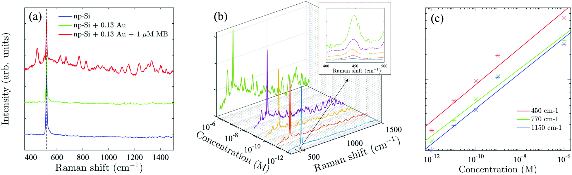 | ||
| Fig. 3 (a) Raman spectra of np-Si (blue), Au/np-Si (green) and Au/np-Si with 1 μM MB (red). The peaks marked by the dash line correspond to the TO phonon mode of silicon. The base lines of the spectra are arbitrarily located on the ordinate; (b) Raman spectra of Au/np-Si with different concentrations of MB, ranging from 1 pM to 1 μM. Inset: The enlarged view of the 450 cm−1 peak; (c) supralinear relationship of concentration and Raman intensity of three Raman peaks at 450 (red), 770 (green), 1150 (blue) cm−1, respectively. | ||
To establish the sensitivity of the method, we measured a series of samples with concentration range between 1 μM and down to the ultra-low 1 pM, shown in Fig. 3(b), with the inset of the zoomed-in range between 400 and 500 cm−1. It can be seen that even for the concentration as low as 1 pM, the MB scattering peak at 450 cm−1 is still detectable, while the further increase of the concentration makes the MB spectral fingerprints more distinct. Fig. 3(c) shows the Raman intensity of the three representative peaks at 450, 770 and 1150 cm−1 (located at short, middle and long spectrum region, respectively) as a function of MB concentration. It can be seen that the intensity increase for these peaks as a function of the concentration is identical. This suggests that the enhancement effect of a Au/np-Si composite does not have spectral selectivity. We note that multiple Raman measurements were taken over random locations on each sample to estimate the mean and deviation (Fig. S8 in the ESI†). The curves shown in Fig. 2(b) are the averages of the Raman spectra measured in those locations. The error bars in Fig. 2(c) represent the peaks’ deviation from their mean values.
The enhancement factor (EF) is an important criterion to evaluate quantitatively the performance of SERS substrates.34,35 As discussed in the literature, there are several ways to determine the EF.58–60 In this work, we adopted an approach that defines it as 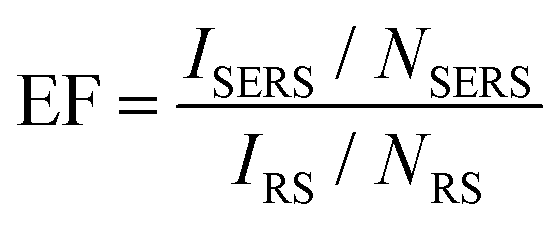 .61ISERS and IRS are the Raman intensities with and without the surface enhancement; NSERS and NRS are the corresponding number of analyte molecules exposed to the beam. For the reference measurement of IRS, a smooth Au film was used as a substrate which was uniformly covered by MB solution with concentration of 100 mM, corresponding to 2.4 × 1012 MB molecules (see Methods) in the area illuminated by the laser. As for the SERS measurement, there are about 24 molecules exposed to the laser at the lowest MB concentration (1 pM). The obtained SERS spectrum is shown by the blue line in Fig. 3(b). The reference Raman spectrum was recorded while keeping the power and spot size of the excitation laser the same as in SERS measurements, (Fig. S1 in the ESI†). The intensity of ISERS and IRS was obtained by integrating the intensity of the three Raman peaks at 450, 770, and 1150 cm−1 which yields 0.196 and 4.063, respectively (abs. unit), and the EF of 4.84 × 10⁹. This is an ample EF value befitting the single molecule detection by the SERS method.34,62 The performance of our substrate approaches that of 3D plasmonic metamaterials with hierarchically ordered porous gold membranes consisting of close-packed arrays of nanoholes and uniformly distributed mesopores over the bulk, where a detection limit down to 10−13 M was demonstrated for non-resonant Raman scattering from benzenethiol molecules.63
Typically, the EF for an isolated Au nanosphere is in the order of 102–104,64–66 which can be further improved to 105–108 by changing its shape,67 the inter-particle spacing64,68,69 or distribution on a substrate.70 The high EF for our SERS substrate can be attributed to the peculiarity of a sponge-like morphological structure of np-Si. Unlike planar substrates used in previous studies, it exhibits an enormous surface for the adsorption of the analyte71 and accommodated gold nanoparticles. The analyte is not only detected on a facet surface of the substrate, but, to a greater extent, across the inner surface of np-Si pore walls. The large surface area of the pores traversing the volume can accommodate the outstanding density of the tightly packed clusters with a large cross-section. These conditions not only allow efficient LSP excitation across the layer depth, but create a large number of ‘hot spots’ where the fields further amplified in narrow gaps between interacting particles. Indeed, Table 2 proposes that particles with the radius as large as 26 nm can be fixed in space with in-between gaps between them of just a few nanometres. Moreover, it is possible to achieve conditions with the interacting particles dominating the assembly. The corresponding spectrum of Fig. 2(e and f) suggests that such tightly interacting particles dominate the response. On the other hand, the material can bind a high density of analyte molecules on the pores surface, in particular in the vicinity of the ‘hot spots’. A similar arrangement is nearly impossible to realise in a liquid phase as the particles will coalesce in that state. Although it is possible to anchor the particles creating narrow gaps on the surface, the number of available sites is limited by the system's low dimensionality. Thus, the 3D np-Si scaffolding with a high density of interacting clusters yields a higher probability of finding molecules in gap areas than in its 2D counterpart and one would, therefore, expect higher overall contribution of amplified SERS response.
2 Conclusions
Au/np-Si composites with varying Au volume fraction were fabricated through the immersion plating technique. The AuNPs were successfully embedded into the 550 nm-thick np-Si substrates, forming a 3D metal/semiconductor composite material. SEM, TEM and EDX analysis confirmed the presence of AuNPs uniformly distributed over the volume. The analysis was used to obtain the average AuNP size and their density, which were employed to simulate LSPR scattering spectra. The numerical modelling suggests that the spectra are characterised by single particle and inter-particle coupling resonances. We examined the potential application to use the composites as a SERS substrate. We demonstrated that the concentration as low as a few picomolar can be detected for the benchmark compound of methylene blue. Our estimates suggest that the enhancement factor of 109 can be achieved on these composite materials. The reason for such high amplification might be attributed to the peculiarities of np-Si. The material can accommodate a large number of metal particles interacting over the entire volume of the substrate containing analyte molecules absorbed in the pores.3 Methods
VIS-NIR spectrometer
The back-scattered light was collected by a PerkinElmer Lambda 1050 UV/Vis/NIR spectrometer equipped with an integrating sphere module. During the measurement, the broad-band, unpolarised halogen light source was used to illuminate the samples. The samples were placed on a port where only the back-reflected light was collected inside the integrating sphere. To exclude the specular component from the diffuse scattered reflectance, a corresponding aperture was opened on the port which allowed the specularly reflected light to exit the integrating sphere.Surface enhanced Raman spectroscopy
An 808 nm laser (Changchun New Industries Optoelectronics Tech. Co., Ltd) was used as the excitation source through a 40× objective (NA 0.6, Plan-Neofluar, Zeiss). The back-scattered Raman signal was collected via the objective after passing through the notch filter (TECHSPEC 808 notch filter, Edmund Optics Inc., Germany). The signal was detected by a spectrograph (Acton Spectra Pro 2500i, Princeton Instruments, Trenton, NJ, USA) equipped with an electron-multiplying charge-coupled device (EMCCD) camera (iXon, Andor, Belfast, UK). Au/np-Si samples with the highest Au volume fraction, f = 0.13, were used as the SERS substrate, while the reference substrate was fabricated by evaporating 100 nm gold onto a 1 cm2 glass slice in a vacuum. Both the Au/np-Si and reference samples were immersed in 2 mL Methylene Blue (MB, high purity, Alfa Aesar) solution. The SERS samples were soaked in solutions with various concentrations in the range between 1 pM and 1 μM, while for the reference the whole volume of 100 mM solution was dropped on the surface. All the samples were dried on a hotplate at 60 °C for 10 min in air. Assuming that all the MB molecules are uniformly adsorbed by the sample, there are ∼2.4 × 10¹² and ∼24 MB molecules on the reference surface and in Au/np-Si volume for 1 pM MB concentration, respectively, exposed to the area of 2 μm2 illuminated by the laser. The obtained Raman spectra for the samples with Au/np-Si as the substrate are shown in Fig. 3(b), while Fig. S1 in the ESI† shows that of the reference.Nano-porous silicon
Nano-porous Si (np-Si) samples were prepared using electrochemical anodisation of a boron doped Si(100) wafer with resistivity in the range of 5–20 mΩ cm, corresponding to a dopant density of 3 × 1018 cm−3. A 1![[thin space (1/6-em)]](https://www.rsc.org/images/entities/char_2009.gif) :1 ratio mixture of methanol and 40% hydrofluoric acid was used as the electrolyte at a current density of 100 mA cm−2 for 8 s to yield an np-Si layer with thickness of approximately 550 nm (measured from the cross-section of the SEM image). The wafer was then rinsed in methanol and dried in air. A 65% porosity was estimated using the gravimetric method.72 The structure of the samples before impregnation can be described as being of a sponge silicon material, consisting of thin flat wires interwoven to form the walls of hollow channels, running along the depth coordinate. The mean thickness of the walls was 10 nm and the diameter of the channels was about 50 nm. The substrates used to fabricate the samples in this study were different from those usually employed to investigate photoluminescence, for which p-silicon substrates are generally better suited.73 Instead, our main focus here was to obtain luminescence-free, optically uniform membranes for which p+ substrates are an established choice.74 For this work, the thickness of the layer was kept sufficiently thin to assure uniform penetration of the gold solution into the depth, while, on the other hand, remaining thick enough to provide an adequate depth to accommodate the laser penetration depth for Raman measurements (see Fig. S9, ESI†). We note that this process could be developed to impregnate layers and membranes with a thickness of more than a hundred microns. With such flexibility one can design an impregnated layered material facilitating an interferometric amplification,33 in addition to SERS.
:1 ratio mixture of methanol and 40% hydrofluoric acid was used as the electrolyte at a current density of 100 mA cm−2 for 8 s to yield an np-Si layer with thickness of approximately 550 nm (measured from the cross-section of the SEM image). The wafer was then rinsed in methanol and dried in air. A 65% porosity was estimated using the gravimetric method.72 The structure of the samples before impregnation can be described as being of a sponge silicon material, consisting of thin flat wires interwoven to form the walls of hollow channels, running along the depth coordinate. The mean thickness of the walls was 10 nm and the diameter of the channels was about 50 nm. The substrates used to fabricate the samples in this study were different from those usually employed to investigate photoluminescence, for which p-silicon substrates are generally better suited.73 Instead, our main focus here was to obtain luminescence-free, optically uniform membranes for which p+ substrates are an established choice.74 For this work, the thickness of the layer was kept sufficiently thin to assure uniform penetration of the gold solution into the depth, while, on the other hand, remaining thick enough to provide an adequate depth to accommodate the laser penetration depth for Raman measurements (see Fig. S9, ESI†). We note that this process could be developed to impregnate layers and membranes with a thickness of more than a hundred microns. With such flexibility one can design an impregnated layered material facilitating an interferometric amplification,33 in addition to SERS.
Gold cluster impregnation
The electroless immersion plating technique was used to impregnate gold clusters into the np-Si layer. The immersion solution was prepared by dissolving 9.85 mg of tetrachloroauric acid (HAuCl4) in 50 mL of ethanol, resulting in a concentration of 0.5 mM. Before the impregnation process, the np-Si sample was dipped in 2% of HF (diluted in DI water) for 30 seconds to remove the native oxide layer developed on the surface of the sample and inside the pores. Afterwards, the np-Si sample was immersed in the pre-mixed HAuCl4 solution and placed in an ultrasonic bath to agitate the solution and stimulate it to flow into the pores. Due to the native surface of pSi which contains metastable Si–Hx termination, the following reaction was triggered near the pore interface: [AuCl4]− + H+ + 3e− = Au + 4Cl− + H+, causing the reduction of Au and formation of Au nanoparticles. After a chosen time period, the sample was rinsed in ethanol and dried in air. Fig. S3 (ESI†) shows the SEM cross section image of sample np-Si + 0.02 Au, and Au clusters can be seen inside the np-Si pore channels. The analysis of the SEM image suggests that the mean diameter of the clusters in this sample is about 20 nm. The picked points in the figure are the random point analysis of a Au nanoparticle, where Da shows the diameter and Db is the area of the selected Au nanoparticle.FEM simulation of single and double AuNP
Comsol Mulitiphysics was used for the simulation of the scattering cross section of single and double Au particles. The particle size was set to 8.1, 14.5, 19.5, and 26.1 nm, respectively, surrounded by a homogeneous material with refractive index of np-Si. The excitation field was set to have both TE and TM components, in order to simulate the experimental condition to a great extent. The wavelength was set to sweep from 500 to 1400 nm. The simulation suggested that the Bruggeman model is only suitable for samples with small Au volume fraction. A correction on the environment dielectric function was applied to fit with the experimental results for high Au volume fraction samples. It also confirmed that the second scattering peak in the measured scattering spectrum came from the coupling between two Au clusters with short separation distance.Conflicts of interest
There are no conflicts to declare.Acknowledgements
The authors thank Dstl for financial support enabled by the grant DSTLX100099482. The authors also thank Alexander Pattison for conducting the TEM experiment.Notes and references
- V. G. Kravets, A. V. Kabashin, W. L. Barnes and A. N. Grigorenko, Chem. Rev., 2018, 118, 5912–5951 CrossRef CAS PubMed.
- K. E. Fong and L.-Y. L. Yung, Nanoscale, 2013, 5, 12043–12071 RSC.
- H. Yu, Y. Peng, Y. Yang and Z.-Y. Li, npj Comput. Mater., 2019, 5, 1–14 CrossRef.
- H. Chen, X. Kou, Z. Yang, W. Ni and J. Wang, Langmuir, 2008, 24, 5233–5237 CrossRef CAS PubMed.
- S. Zeng, D. Baillargeat, H.-P. Ho and K.-T. Yong, Chem. Soc. Rev., 2014, 43, 3426–3452 RSC.
- J.-F. Masson, Analyst, 2020, 145, 3776–3800 RSC.
- N. Zhou, V. López-Puente, Q. Wang, L. Polavarapu, I. Pastoriza-Santos and Q.-H. Xu, RSC Adv., 2015, 5, 29076–29097 RSC.
- A. Aubry, D. Y. Lei, A. I. Fernández-Domnguez, Y. Sonnefraud, S. A. Maier and J. B. Pendry, Nano Lett., 2010, 10, 2574–2579 CrossRef CAS PubMed.
- Y. Y. Lee, R. M. Kim, S. W. Im, M. Balamurugan and K. T. Nam, Nanoscale, 2020, 12, 58–66 RSC.
- W. P. Hall, J. N. Anker, Y. Lin, J. Modica, M. Mrksich and R. P. Van Duyne, J. Am. Chem. Soc., 2008, 130, 5836–5837 CrossRef CAS PubMed.
- Y. Leroux, J. C. Lacroix, C. Fave, V. Stockhausen, N. Félidj, J. Grand, A. Hohenau and J. R. Krenn, Nano Lett., 2009, 9, 2144–2148 CrossRef CAS PubMed.
- J. Ki, H. Y. Lee, H. Y. Son, Y.-M. Huh and S. Haam, ACS Appl. Mater. Interfaces, 2019, 11, 18923–18929 CrossRef CAS.
- A. J. Haes, L. Chang, W. L. Klein and R. P. Van Duyne, J. Am. Chem. Soc., 2005, 127, 2264–2271 CrossRef CAS PubMed.
- D. Furtado, M. Björnmalm, S. Ayton, A. I. Bush, K. Kempe and F. Caruso, Adv. Mater., 2018, 30, 1801362 CrossRef PubMed.
- M. J. Natan, M. D. Musick, C. Keating and K. R. Brown, SERS substrates formed by hydroxylamine seeding of colloidal metal nanoparticle monolayers, US Pat., 6624886, 2003 Search PubMed.
- T. R. Jensen, M. D. Malinsky, C. L. Haynes and R. P. Van Duyne, J. Phys. Chem. B, 2000, 104, 10549–10556 CrossRef CAS.
- F.-C. Chen, J.-L. Wu, C.-L. Lee, Y. Hong, C.-H. Kuo and M. H. Huang, Appl. Phys. Lett., 2009, 95, 182 Search PubMed.
- M. Kahraman, E. R. Mullen, A. Korkmaz and S. Wachsmann-Hogiu, Nanophotonics, 2017, 6, 831–852 CAS.
- G. Demirel, H. Usta, M. Yilmaz, M. Celik, H. A. Alidagi and F. Buyukserin, J. Mater. Chem. C, 2018, 6, 5314–5335 RSC.
- I. Pastoriza-Santos, C. Kinnear, J. Pérez-Juste, P. Mulvaney and L. M. Liz-Marzán, Nat. Rev. Mater., 2018, 3, 375–391 CrossRef.
- Z. Y. Bao, D. Y. Lei, R. Jiang, X. Liu, J. Dai, J. Wang, H. L. W. Chan and Y. H. Tsang, Nanoscale, 2014, 6, 9063–9070 RSC.
- J. Sasai and K. Hirao, J. Appl. Phys., 2001, 89, 4548–4553 CrossRef CAS.
- R. Cui, C. Liu, J. Shen, D. Gao, J.-J. Zhu and H.-Y. Chen, Adv. Funct. Mater., 2008, 18, 2197–2204 CrossRef CAS.
- N. Pinçon, B. Palpant, D. Prot, E. Charron and S. Debrus, Eur. Phys. J. D, 2002, 19, 395–402 CrossRef.
- N. Waiskopf, Y. Ben-Shahar and U. Banin, Adv. Mater., 2018, 30, 1706697 CrossRef PubMed.
- G. Yu, X. Wang, J. Cao, S. Wu, W. Yan and G. Liu, Chem. Commun., 2016, 52, 2394–2397 RSC.
- K. H. W. Ho, A. Shang, F. Shi, T. W. Lo, P. H. Yeung, Y. S. Yu, X. Zhang, K.-y. Wong and D. Y. Lei, Adv. Funct. Mater., 2018, 28, 1800383 CrossRef.
- T. Kormilina, E. Stepanidenko, S. Cherevkov, A. Dubavik, M. Baranov, A. Fedorov, A. Baranov, Y. Gun'Ko and E. Ushakova, J. Mater. Chem. C, 2018, 6, 5278–5285 RSC.
- J. Li, S. K. Cushing, P. Zheng, T. Senty, F. Meng, A. D. Bristow, A. Manivannan and N. Wu, J. Am. Chem. Soc., 2014, 136, 8438–8449 CrossRef CAS PubMed.
- J.-H. Zhong, J. Vogelsang, J.-M. Yi, D. Wang, L. Wittenbecher, S. Mikaelsson, A. Korte, A. Chimeh, C. L. Arnold, P. Schaaf, E. Runge, A. L'Huillier, A. Mikkelsen and C. Lienau, Nat. Commun., 2020, 11, 1–10 Search PubMed.
- L. Canham, Handbook of porous silicon, Springer, 2014 Search PubMed.
- A. Zakar, R. Wu, D. Chekulaev, V. Zerova, W. He, L. Canham and A. Kaplan, Phys. Rev. B, 2018, 97, 155203 CrossRef CAS.
- W. He, R. Wu, I. V. Yurkevich, L. T. Canham and A. Kaplan, Sci. Rep., 2018, 8, 1–7 Search PubMed.
- E. Le, Ru, E. Blackie, M. Meyer and P. G. Etchegoin, J. Phys. Chem. C, 2007, 111, 13794–13803 CrossRef.
- P. Mao, C. Liu, G. Favraud, Q. Chen, M. Han, A. Fratalocchi and S. Zhang, Nat. Commun., 2018, 9, 1–8 CrossRef CAS.
- N. R. Jana, L. Gearheart and C. J. Murphy, J. Phys. Chem. B, 2001, 105, 4065–4067 CrossRef CAS.
- M. Grzelczak, J. Pérez-Juste, P. Mulvaney and L. M. Liz-Marzán, Chem. Soc. Rev., 2008, 37, 1783–1791 RSC.
- D. E. Newbury, Scanning: The Journal of Scanning Microscopies, 2009, 31, 91–101 CrossRef CAS PubMed.
- K. Minami, Y. Saito, H. Kai, K. Shirota and K. Yada, J. Phys.: Conf. Ser., 2009, 012010 CrossRef.
- G.-C. Li, Y.-L. Zhang and D. Y. Lei, Nanoscale, 2016, 8, 7119–7126 RSC.
- H. Frohlich, Theory of Dielectrics, 2nd edn, 1958, vol. 57, pp. 592–601 Search PubMed.
- S. Nath, S. K. Ghosh, S. Praharaj, S. Panigrahi, S. Basu and T. Pal, New J. Chem., 2005, 29, 1527–1534 RSC.
- P. Nordlander, C. Oubre, E. Prodan, K. Li and M. Stockman, Nano Lett., 2004, 4, 899–903 CrossRef CAS.
- W. Rechberger, A. Hohenau, A. Leitner, J. Krenn, B. Lamprecht and F. Aussenegg, Opt. Commun., 2003, 220, 137–141 CrossRef CAS.
- R. Wu, T. Mathieu, C. J. Storey, Q. Jin, J. Collins, L. T. Canham and A. Kaplan, Adv. Opt. Mater., 2021, 9, 2002119 CrossRef CAS.
- P. B. Johnson and R.-W. Christy, Phys. Rev. B, 1972, 6, 4370 CrossRef CAS.
- D. Bruggeman, Ann. Phys. Leipzig, 1935, 24, 636 CrossRef CAS.
- M. Khardani, M. Bouacha and B. Bessas, Phys. Status Solidi C, 2007, 4, 1986–1990 CrossRef CAS.
- C. F. Bohren and D. R. Huffman, Absorption and Scattering of light by small particles, John Wiley and Sons, Inc., NY, 1983 Search PubMed.
- G.-N. Xiao and S.-Q. Man, Chem. Phys. Lett., 2007, 447, 305–309 CrossRef CAS.
- A. Kaminska, O. Inya-Agha, R. J. Forster and T. E. Keyes, Phys. Chem. Chem. Phys., 2008, 10, 4172–4180 RSC.
- P. Spizzirri, J.-H. Fang, S. Rubanov, E. Gauja and S. Prawer, 2010, arXiv preprint arXiv:1002.2692.
- C. Li, Y. Huang, K. Lai, B. A. Rasco and Y. Fan, Food Control, 2016, 65, 99–105 CrossRef CAS.
- C. Srichan, M. Ekpanyapong, M. Horprathum, P. Eiamchai, N. Nuntawong, D. Phokharatkul, P. Danvirutai, E. Bohez, A. Wisitsoraat and A. Tuantranont, Sci. Rep., 2016, 6, 23733 CrossRef CAS PubMed.
- S. D. Roy, P. Sett, M. Ghosh and J. Chowdhury, J. Raman Spectrosc., 2017, 48, 38–45 CrossRef CAS.
- R. R. Naujok, R. V. Duevel and R. M. Corn, Langmuir, 1993, 9, 1771–1774 CrossRef CAS.
- K.-D. Shim and E.-S. Jang, Bull. Korean Chem. Soc., 2018, 39, 936–940 CrossRef CAS.
- Y. Wang, H. Chen, S. Dong and E. Wang, J. Chem. Phys., 2006, 124, 074709 CrossRef.
- M. Green and F. M. Liu, J. Phys. Chem. B, 2003, 107, 13015–13021 CrossRef CAS.
- K. Wu, L. Q. Nguyen, T. Rindzevicius, S. S. Keller and A. Boisen, Adv. Opt. Mater., 2019, 7, 1901413 CrossRef CAS.
- E. C. Le Ru and P. G. Etchegoin, MRS Bull., 2013, 38, 631 CrossRef.
- E. J. Blackie, E. C. Le Ru and P. G. Etchegoin, J. Am. Chem. Soc., 2009, 131, 14466–14472 CrossRef CAS PubMed.
- X. Zhang, Y. Zheng, X. Liu, W. Lu, J. Dai, D. Y. Lei and D. R. MacFarlane, Adv. Mater., 2015, 27, 1090–1096 CrossRef CAS PubMed.
- L. Litti and M. Meneghetti, Phys. Chem. Chem. Phys., 2019, 21, 15515–15522 RSC.
- D.-S. Wang and M. Kerker, Phys. Rev. B, 1981, 24, 1777 CrossRef CAS.
- V. Joseph, A. Matschulat, J. Polte, S. Rolf, F. Emmerling and J. Kneipp, J. Raman Spectrosc., 2011, 42, 1736–1742 CrossRef CAS.
- C. Hrelescu, T. K. Sau, A. L. Rogach, F. Jäckel and J. Feldmann, Appl. Phys. Lett., 2009, 94, 153113 CrossRef.
- S. L. Kleinman, B. Sharma, M. G. Blaber, A.-I. Henry, N. Valley, R. G. Freeman, M. J. Natan, G. C. Schatz and R. P. Van Duyne, J. Am. Chem. Soc., 2013, 135, 301–308 CrossRef CAS PubMed.
- S. Hong and X. Li, J. Nanomater., 2013, 2013, 790323, DOI:10.1155/2013/790323.
- A. Wei, B. Kim, B. Sadtler and S. L. Tripp, Chem. Phys. Chem., 2001, 2, 743–745 CrossRef CAS.
- S. A. Trauger, E. P. Go, Z. Shen, J. V. Apon, B. J. Compton, E. S. Bouvier, M. Finn and G. Siuzdak, Anal. Chem., 2004, 76, 4484–4489 CrossRef CAS PubMed.
- R. Wu, J. Collins, L. Canham and A. Kaplan, Appl. Sci., 2018, 8, 1810 CrossRef.
- J. Joo, T. Defforge, A. Loni, D. Kim, Z. Li, M. J. Sailor, G. Gautier and L. T. Canham, Appl. Phys. Lett., 2016, 108, 153111 CrossRef.
- A. Campos, J. Torres and J. Giraldo, Surf. Rev. Lett., 2002, 9, 1631–1635 CrossRef CAS.
Footnotes |
| † Electronic supplementary information (ESI) available. See DOI: 10.1039/d1nh00228g |
| ‡ Contributed equally to this work. |
| This journal is © The Royal Society of Chemistry 2021 |