
Real-time insight into nanostructure evolution during the rapid formation of ultra-thin gold layers on polymers†
Matthias
Schwartzkopf
 *a,
Sven-Jannik
Wöhnert
a,
Vivian
Waclawek
a,
Niko
Carstens
b,
André
Rothkirch
a,
Jan
Rubeck
a,
Marc
Gensch
ac,
Jonas
Drewes
b,
Oleksandr
Polonskyi
b,
Thomas
Strunskus
b,
Alexander M.
Hinz
b,
Simon J.
Schaper
c,
Volker
Körstgens
c,
Peter
Müller-Buschbaum
cd,
Franz
Faupel
b and
Stephan V.
Roth
ae
*a,
Sven-Jannik
Wöhnert
a,
Vivian
Waclawek
a,
Niko
Carstens
b,
André
Rothkirch
a,
Jan
Rubeck
a,
Marc
Gensch
ac,
Jonas
Drewes
b,
Oleksandr
Polonskyi
b,
Thomas
Strunskus
b,
Alexander M.
Hinz
b,
Simon J.
Schaper
c,
Volker
Körstgens
c,
Peter
Müller-Buschbaum
cd,
Franz
Faupel
b and
Stephan V.
Roth
ae
aPhoton Science, Deutsches Elektronen-Synchrotron (DESY), Notkestr. 85, D-22607 Hamburg, Germany. E-mail: matthias.schwartzkopf@desy.de
bLehrstuhl für Materialverbunde, Institut für Materialwissenschaft, Christian Albrechts-Universität zu Kiel, Kaiserstr. 2, D-24143 Kiel, Germany
cLehrstuhl für Funktionelle Materialien, Physik-Department, Technische Universität München, James-Franck-Str. 1, D-85748 Garching, Germany
dHeinz Maier-Leibniz Zentrum (MLZ), Technische Universität München, Lichtenbergstraße. 1, D-85748 Garching, Germany
eKTH Royal Institute of Technology, Department of Fibre and Polymer Technology, Teknikringen 56-58, SE-100 44 Stockholm, Sweden
First published on 25th November 2020
Abstract
Ultra-thin metal layers on polymer thin films attract tremendous research interest for advanced flexible optoelectronic applications, including organic photovoltaics, light emitting diodes and sensors. To realize the large-scale production of such metal–polymer hybrid materials, high rate sputter deposition is of particular interest. Here, we witness the birth of a metal–polymer hybrid material by quantifying in situ with unprecedented time-resolution of 0.5 ms the temporal evolution of interfacial morphology during the rapid formation of ultra-thin gold layers on thin polystyrene films. We monitor average non-equilibrium cluster geometries, transient interface morphologies and the effective near-surface gold diffusion. At 1 s sputter deposition, the polymer matrix has already been enriched with 1% gold and an intermixing layer has formed with a depth of over 3.5 nm. Furthermore, we experimentally observe unexpected changes in aspect ratios of ultra-small gold clusters growing in the vicinity of polymer chains. For the first time, this approach enables four-dimensional insights at atomic scales during the gold growth under non-equilibrium conditions.
New conceptsPrimarily based on molecular dynamic simulations and static investigations close to equilibrium conditions, the mechanisms of hybrid nanomaterial assembly seem to be relatively well understood. However, direct observation and quantification of relevant metastable non-equilibrium interface morphologies, especially during early growth stages, remain utmost challenging. Exploiting for the first time surface-sensitive X-ray scattering on time-scales relevant for ultra-small clusters combined with advanced imaging algorithms, we directly visualize the rapid formation of ultra-thin gold cluster layers in the vicinity of polymer chains. Our present study provides novel and direct insights into transient metal–polymer interfacial morphologies including metal nucleation far away from equilibrium in real-time. The sub-surface gold doping of the polymer matrix is temporally and spatially quantified and unexpected changes in aspect ratios of ultra-small gold clusters during the nascence of a hybrid material are experimentally witnessed for the first time. All these findings play a key role in efficient, controlled and resource-saving concepts for integrating functional thin film devices in modern information and energy harvesting technology. This novel real-time approach can be extended to the design of hybrid nanomaterials in heterogeneous multifunctional optoelectronic devices. |
Introduction
The relevance of functional metal–polymer composites for practical applications has seen a steep rise in recent years due to their high device performance, mechanical flexibility and cost-efficient production.1 They cover a broad spectrum of attractive applications such as metal–organic photovoltaics,2,3 light emitting diodes,4 field effect transistors,5 fuel cells6 and sensors.7 Depending on their application, an efficient tailoring of relevant structures on different length scales down to nanometer scale and below is required to fully exploit their great potential.8–11 Therefore, sputter deposition as a versatile bottom-up procedure stands out to rapidly fabricate nanostructures with desired properties for the envisioned application.1,12,13 In case of high rate gold sputter deposition on amorphous polymer thin films, atomistic rate equations describing a local equilibrium can only be applied to a limited extent.14,15 The incoming atoms impinge on a rather smooth and flexible interface with an average kinetic energy around 5 eV, respectively an impact velocity of 2 km s−1.16,17 After the kinetic energy of the incoming atoms has dissipated by inelastic collisions, the adatoms continue to diffuse in close vicinity to the macromolecules. Starting from extremely mobile dimers after adatom collision, each additionally adsorbed atom causes changes in the intrinsic cluster stability. Thus, a large variety of ephemeral isomeric ultra-small Au clusters with different outer shapes and inner configurational arrangements often coexist and interconvert.18 Consequently, for Au clusters growing under non-equilibrium conditions near macromolecules, the different physicochemical environments such as coils, cavities, kinks, terminal groups and side chains, affect the temporary morphology and quasi equilibrium descriptions are no longer valid.The mechanisms of nucleation and growth of supported noble metals is only relatively well understood close to equilibrium primarily based on investigations of interface morphologies, with local real-time transmission electron microscopy (TEM) or kinetic Monte-Carlo, respectively, molecular dynamics simulations.19–24 Therefore, an experimental determination at the atomic level in real time is required to facilitate direct observations of the transient nanoscale interface morphologies of ultra-small metal clusters growing on macromolecules far away from equilibrium conditions. Advanced synchrotron-based surface-sensitive X-ray scattering demonstrated its potential to access three-dimensional information on the average electron density distributions statistically averaged over macroscopic dimensions under in situ or operando conditions.25–33 However, real-time studies with atomic insights regarding the rapid changes of the initial metastable gold cluster geometries towards equilibrium are still missing, in particular during industrial-style, high rate sputter deposition on polymeric interfaces.
In this study, we exploit high brilliance synchrotron radiation and next generation X-ray detectors to follow the nanoscale structure formation processes in situ with sub-millisecond grazing-incidence small-angle X-ray scattering (GISAXS) during rapid Au sputter deposition on as-spun atactic polystyrene (PS) thin films as a comparatively well investigated model system for weak polymer–metal interaction with a high electron density contrast.34 This approach enables us to elucidate different growth regimes in situ and in real-time with unprecedented time resolution to render in more detail the changes of the non-equilibrium cluster morphology during the early stages of sputter deposition, being one of the most important physical vapour deposition processes. We obtain novel statistically relevant insights at the nanoscale to observe partial coalescence phenomena and anticipate kinetics in the nucleation regime even during high rate deposition conditions, which were far out of the time resolution of previous experiments.
Results and discussion
Polymer–metal interface morphology
The static topography measured by atomic force microscopy (AFM) from the pristine as-spun PS thin film (Fig. 1a) shows a smooth surface with a local root-mean-square roughness of σrms = 0.1 nm. The average peak-to-valley distance is around 0.3 nm, which is comparable to the roughness and topography of a native silicon oxide layer SiOx grown at ambient conditions.35,36 After 1 s of industrial-style sputter deposition on the as-spun PS film, the top-most interface becomes rapidly decorated with a dense nanogranular Au cluster layer. The kinetically-trapped assembly is primarily composed of polydisperse spheroidal Au nanoclusters in a rather disordered arrangement (Fig. 1b). Fig. 1c shows a cross-sectional scheme of the resulting nanocomposite layer morphology, where the supported spheroidal Au clusters are characterized by height H, radius R and interparticle distance D. Spin-cast PS thin films on silicon (Si/SiOx) substrates feature a high degree of correlated interfacial roughness causing strong X-ray thin film interferences (XTFI) related to a constructive interference of X-rays in between the interfaces.27,36,37 Note that this key feature often represent the strongest GISAXS signals and is directly connected to electron density correlation in between the Si/PS and PS/Au interfaces.26,27,36 Based on neutron reflectivity, radiotracer detection and positron annihilation light spectroscopy (PALS), it is known that spin-cast atactic PS thin films have a certain free volume fraction providing potential diffusion pathways for metal adatoms.36,38,39 Thus, oversaturation with highly mobile Au atoms during the early stages of sputter deposition cause an occasional subplantation and a gold/polymer enrichment layer AuPS in the near surface region.30,40 | ||
| Fig. 1 Polymer–metal interface morphology: AFM topography of (a) the as-spun polystyrene thin film and (b) after t = 1 s Au sputter deposition with a rate J = 1.52 nm s−1 in a kinetically trapped state. (c) Cross-sectional scheme of the interface morphology of the as-spun Si/SiOx/PS substrate with film thickness dPS and the final kinetically trapped Si/SiOx/PS/AuPS/Au nanocomposite multilayer. The near surface oversaturation with Au during high rate sputter deposition results in a correlated AuPS-enrichment layer with a thickness dAuPS. The supported nanogranular Au layer consists of spheroidal clusters characterized by height H, radius R and interparticle distance D. (d) GISAXS image corresponding to 0.1 s exposure time from as-spun PS thin film before and (e) at the end of high-rate Au sputter deposition around an effective deposited layer thickness of dAu = (3.8 ± 0.1) nm. | ||
The as-spun PS thin film (Fig. 1d) shows several prominent characteristic GISAXS features primarily along the reflection plane: (i) the specular reflected X-ray beam at αf = αi = 0.390°; (ii) at the critical angles αc,PS = 0.093° and αc,Si = 0.134°,respectively, the so-called Yoneda peaks originating from a total external reflection forming a Yoneda band and (iii) intermediary XTFI pattern (ESI,† Fig. S2).41 The latter material specific feature is, besides the specular reflection, the strongest signal directly connected to the electron density correlation and contrast at the interfaces.42 Thus, the temporal evolution of this predominant key scattering feature is very sensitive to the deposition of high Z materials (such as Au) even at sub-millisecond time resolution. The frequency of the XTFI pattern depends on the thin PS film thickness dPS, whereas the damping of the amplitude at higher interference orders is connected to the degree of correlation in interface roughness.43 In order to quantify the specific nature of the observed XTFI in our experiment in view of the parameters layer thickness dPS, layer dispersion δPS and layer roughness σrms including the multiple scattering events at a graded interface,26,43 a sequence of IsGISAXS simulations has been carried out (ESI,† Fig. S3).44 The following general tendencies are derived: (i) an increase of dPS will increase the number of XTFI peaks and reduce their distances in between the Yoneda peaks; (ii) the increase of correlated layer roughness σrms will only reduce the amplitude of XTFI pattern above the critical angle of Si but the XTFI peaks in the Yoneda band stay unaffected and (iii) an increase of the layer dispersion δPS causes a compression of the Yoneda band towards the Si critical angle resulting in a decrease of the distances of XTFI peaks. Good agreement to the data of the pristine PS film (ESI,† Fig. S2) was obtained assuming a film thickness of dPS = (88 ± 2) nm and a δPS,0 = 1.3264 × 10⁻⁶ comparable to the PS bulk dispersion. Considering the absence of any significant out-of-plane scattering intensity along qy, the pristine PS thin film shows no predominant lateral nanostructures or domains on the length scales relevant for atomic self-organization. In contrast, at the end of high-rate Au sputter deposition for an effective deposited Au layer thickness of dAu = (3.8 ± 0.1) nm (Fig. 1e), the out-of-plane peak position and shape indicate a nanogranular morphology induced by the rapid atomic self-organization.
However, these static data provides no further insights into the kinetics of the non-equilibrium processes during structure formation happened on a very fast timescale before.
Real-time insight into nanostructure evolution
The real-time GISAXS experiment performed at a 3rd generation synchrotron (P03, PETRA III)45 combined with automatized data evaluation via a directly programmable data analysis kit (DPDAK)46 are described in more detail in the ESI† (Fig. S1). The resulting three contour plots in Fig. 2 visualize the time-resolved evolution of the key scattering features derived from each single pattern during Au sputter deposition on PS homopolymer thin film.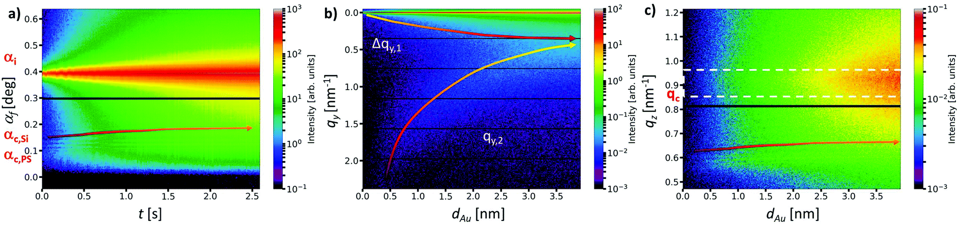 | ||
| Fig. 2 Evolution of key interface scattering features: (a) temporal evolution of the intensity distribution along the reflection plane depicted as scattering exit angle αf during high rate sputter deposition. The corresponding shift of XTFI (arrow), incident angle αi = 0.390°, critical angle of polystyrene αc,PS = 0.093° and silicon αc,Si = 0.134° are indicated. (b) Evolution of the intensity distribution across the reflection plane depicted as scattering vector qy as a function of effective Au thickness dAu. The intensity distribution Δqy,1 around the qy = 0 nm−1 broadens from the beginning of sputter deposition. The out-of-plane intensity distribution qy,2 shifts continuously towards smaller scattering vectors. (c) Effective Au thickness dAu evolution of the out-of-plane intensity distribution along the reflection plane depicted as scattering vector qz shows the non-linear shift of XTFI (colored arrow) and the intensity increase above the critical angle of Au ranging from qc = 0.85 nm−1 to 0.95 nm−1 (white dashed box). | ||
The temporal in plane intensity evolution along the reflection plane as a function of exit angle I(αf,t) in Fig. 2a provides insights in changes of electron density distributions parallel to the surface during the very fast nanostructure formation with a 0.5 ms time resolution. The intensity distribution across the reflection plane I(qy,dAu) as a function of the corresponding scattering vector qy and the effective gold layer thickness dAu visualizes the connection between the effective deposited amount of Au and the average lateral cluster morphology in the near surface regime (Fig. 2b). In order to further quantify the increase of electron density distribution vertically at the Au/PS interface during sputter deposition, an additional vertical integration of the out-of-plane intensity distribution was performed along the scattering vector qz (Fig. 2c).
The temporal evolution of the XTFI peak positions in between the Yoneda peaks of PS and Si revealed a non-linear equidistant shift towards higher scattering angles (Fig. 2a and ESI,† Fig. S7). This is consistent with an increase of the layer dispersion δPS of the polymer matrix counterbalanced by a simultaneous decrease of the correlated interface distance dPS. In other words, the sub-surface enrichment of Au forms a different effective medium in terms of thickness and density directly affecting the propagation and interference of the X-rays. Thus, the average volume fraction of gold fAu in the PS layer can be described as follows:
| fAu(δPS) ≈ (δPS(t) − δPS,0)/(δAu − δAu,0), | (1) |
 | ||
| Fig. 3 Evolution of key interface feature sizes: (a) temporal evolution of filling factor fAu and polystyrene correlated layer thickness dPS. (b) Effective Au layer thickness evolution of interparticle distances D, radii R and particle height H. The Roman numbers indicate the growth regimes: (I) nucleation and growth; (II) diffusion-mediated growth; (III) adsorption-mediated growth and (IV) layer growth. (c) Height to radius aspect ratio H/R of a spheroid (black), average cluster density ρ (red) and number of atoms per cluster NAu (blue) on a logarithmic time scale with initial sub-regimes: Ia adatoms; Ib ultra-small clusters; Ic coalescing 3D clusters. | ||
The height-to-radius aspect ratio H/R represents the evolution of average cluster shapes during growth.
Furthermore, considering that in total only half of a cluster covers the trigonal unit cell defined by D, the maximum cluster densities are calculated by ρ = 2/√3D2 and plotted as number per cm2 (Fig. 3c). In addition, the average numbers of atoms per cluster are calculated by the volume ratio of a spheroidal cluster and the spherical volume of an Au atom NAu = 0.5R2H/rAu3 assuming a spheroidal shape may conveniently grasp the average cluster shapes induced by non-equilibrium coalescence.21
The nascence of a metal–polymer-hybrid material
For the first time, high time resolution during sub-millisecond GISAXS enables atomic insights in the nucleation regime, and a further partitioning into sub-regimes based on non-equilibrium transient changes of the clusters’ aspect ratio becomes feasible. The obtained results suggest different competing growth mechanisms being relevant and present for ultra-small clusters in the nucleation regime. The essence of the observed morphological changes from electron density variations parallel and perpendicular to surface normal is schematically drawn in Fig. 4 and will be summarized as follows: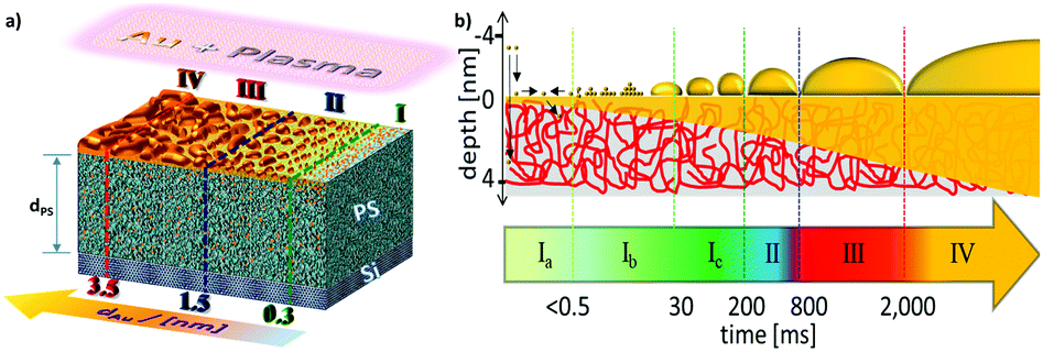 | ||
| Fig. 4 Evolution of the metal–polymer interface morphology: (a) schematically scaled representation of the transient interface morphology evolution and sub-surface enrichment of gold atoms in the four growth regimes during sputter deposition on PS/Si thin films. (b) Cross-sectional scheme of average non-equilibrium cluster shapes and of the interface morphology during the rapid formation of ultra-thin gold layers on the polymer layer. The Roman numbers indicate the different growth regimes described in the main text. | ||
Sputter deposition starts with the nucleation and growth regime (I), where the particle density increases up to the effective film thickness dAu,I = 0.27 nm being equivalent to an Au monolayer (Fig. 3c). The cluster distances D slightly decrease by the establishment of new nuclei (Fig. 3b). Average radii R are continuously increasing, which is in accordance with a predominance of nucleation processes over coalescence phenomena. Based on our experiment, this regime starts with landing, accommodation, and collisions of adatoms on microsecond time scales (Ia, Fig. 4b), which we cannot resolve in this experiment. The energy dissipation from the sputter deposition is primarily conserved in the metal fraction promoting diffusivity of adatoms and small clusters as the heat capacity of macromolecules is poor compared to free moving metal atoms. At the top-most thin film interface, the PS chains expose higher mobility enabling sub-surface diffusion.17 Since most of the macromolecular substrate is uncovered, the sub-surface diffusion of gold atoms is significant in the early stages of sputter deposition. The first deduced average cluster distances are around D = (3.8 ± 1.5) nm. The average cluster heights around H = (0.53 ± 2.08) nm are slightly larger than the atomic diameter of gold while the first average cluster radii R = (0.17 ± 0.04) nm nearly match that of the atomic radius rAu = 0.144 nm. This hints that single gold adatoms and vertical dimers are the most prominent species after 0.5 ms of sputter deposition. An unusual high H/R aspect ratio in the early stages of metal cluster formation has been predicted to be even a factor 2 higher by molecular dynamics (MD) simulations based on Langevin equations.22 According to DFT calculations, vertical Au dimers can exist for weak substrate interactions and planar geometries can be favored for ultra-small Au clusters.18,20,49,50 In this sub-regime (Ib), such planar ultra-small two-dimensional clusters, vertical dimers and adatoms coexist and permanently coalesce.51 The particle density ρ is almost constant indicating the high mobility and coalescence capability of such ultra-small clusters. Thus, each additionally adsorbed adatom challenges the intrinsic cluster stability, which causes many isomeric non-equilibrium cluster structures to interconvert in this regime.52 This competitive growth results in a continuous decrease of average H/R aspect ratio towards a local minimum indicating a threshold to sub-regime Ic after 30 ms. Here, the nascent Au clusters above NAu > 55 tend to grow as truncated spheres in parallel to the perpetually emerging ultra-small clusters leading to a temporary increase of H/R and ρ. Furthermore, due to topological and quantum mechanical effects, a transition from the semiconductor to metallic properties occurs due to overlapping of valence and conduction band.53 This size-induced metal–insulator transition is correlated with a dramatic increase of intracluster electron mobility, and localized surface plasmons can be excited.53,54 After 200 ms sputter deposition respectively dAu > 0.27 nm, in the diffusion-mediated regime (II) adjacent cluster coalescence leads to formation of bottleneck-type boundary zones and gradually fusion into bigger, dumbbell-elongated non-equilibrium clusters.21,51 Cluster mobility and coalescence velocity are increasingly restricted and their surface coverage of the immobilized elongated clusters allows for primarily adsorbing new gold atoms directly from the gaseous phase.19,30,55 Subsequently, in this adsorption-mediated regime (III) above effective thicknesses dAu > 1.5 nm, sub-surface diffusion plays a minor role and permanent cluster coalescence further reduce H/R aspect ratio and induces a kinetically trapped ramification. At an effective layer thickness of dAu > 3.5 nm, the layer growth regime (IV) sets in as soon as the ramification reaches the so-called percolation threshold, where all clusters tend to interconnect to a conductive fractal network (Fig. 4a).31,56 The lateral expansion becomes sterically hindered, distances and radii growth rates become reduced and the average cluster heights approach the effective layer thickness (Fig. 4b).
Conclusions
In conclusion, this first sub-millisecond real-time GISAXS study enables atomic insights in the formation of ultra-thin Au cluster layers and contributes to a more complete picture of chemical inert atomic self-assembly during sputter deposition on macromolecular thin films. For the first time, we quantify earliest non-equilibrium cluster geometries and near-surface embedding at industrial-relevant deposition rates. The observed near-surface AuPS enrichment layer promotes metal layer adhesion of gold on polymers fabricated by sputter deposition.57 The sub-surface enrichment up to a 2% gold volume fraction being more dominant in the early stages around an effective thickness of 1 nm, may be useful to dope intentionally functional polymer layers with metal atoms.58 Already dAu ≈ 0.3 nm gold sputter deposition on a thin PS/Si film, for example, changes the thermodynamic behavior significantly and no thin film rupture occurs even after long-time annealing at temperatures well above 150 °C.59 For some delicate applications e.g. memristors or light emitting diodes, this atomic doping effect during electrode formation via sputter deposition may alter their device performance.60,61 We believe that the hereby obtained evolution of morphological parameters of ultra-small nanoclusters serve as benchmarks for integrating tailored hybrid nanomaterials in modern information and energy harvesting technologies. This novel real-time approach can be extended to systematically quantify the impact of deposition conditions, e.g. different substrate temperatures or target/substrate material compositions, allowing for a targeted design of hybrid nanomaterials in heterogeneous multifunctional optoelectronic devices. Ultimately, our study will enable the investigation of metastable interface morphologies even of ultra-thin films made of abundant and application-relevant low Z compounds, exploiting the emerging 4th generation diffraction limited storage rings and 4th generation free electron lasers.Authors contribution
For this experiment at large scale facility the authors Matthias Schwartzkopf, Sven-Jannik Wöhnert, Niko Carstens, Jan Rubeck, André Rothkirch, Marc Gensch, Jonas Drews, Oleksandr Polonskyi, Thomas Strunskus, Simon J. Schaper, and Volker Körstgens contributed to the alignment of X-ray optics, set up of the sputter chamber at the beamline and performed the in situ GISAXS measurements. Alexander M. Hinz designed the sputter chamber and participated in preliminary experiments. Matthias Schwartzkopf analyzed the data, performed IsGISAXS simulations and created all figures. The preparation of polymer templates and static Au/PS/Si samples including AFM measurements were performed by Vivian Waclawek. Stephan V. Roth, Franz Faupel and Peter Müller-Buschbaum provided materials and supervision and participated in the interpretation of the data. The manuscript was written with contributions of all authors and all have given approval to the final version of the manuscript.Conflicts of interest
The authors declare no competing interests.Acknowledgements
The authors acknowledge the Deutsche Forschungsgemeinschaft (DFG) for funding under the projects RO 4638/1-1/2, FA 234/23-1/2 and MU 1487/18-1/2. The authors would like to thank Dr David Pennicard and X-Spectrum GmbH for their help with the LAMBDA detector. Major parts of this research were carried out at the light source PETRA III at DESY, a member of the Helmholtz Association (HGF).References
- F. Faupel, V. Zaporojtchenko, T. Strunskus and M. Elbahri, Adv. Eng. Mater., 2010, 12, 1177–1190 CrossRef CAS.
- E. Stratakis and E. Kymakis, Mater. Today, 2013, 16, 133–146 CrossRef CAS.
- M. Westphalen, U. Kreibig, J. Rostalski, H. Lu and D. Meissner, Sol. Energy Mater. Sol. Cells, 2000, 61, 97–105 CrossRef CAS.
- P. A. Hobson, S. Wedge, J. A. E. Wasey, I. Sage and W. L. Barnes, Adv. Mater., 2002, 14, 1393–1396 CrossRef CAS.
- M. L. Hammock, A. N. Sokolov, R. M. Stoltenberg, B. D. Naab and Z. Bao, ACS Nano, 2012, 6, 3100–3108 CrossRef CAS.
- R.-C. Zhang, D. Sun, R. Zhang, W. Lin, M. Macias-Montero, J. Patel, S. Askari, C. McDonald, D. Mariotti and P. Maguire, Sci. Rep., 2017, 7, 46682 CrossRef.
- J. Li, J. Liang, L. Li, F. Ren, W. Hu, J. Li, S. Qi and Q. Pei, ACS Nano, 2014, 8, 12874–12882 CrossRef CAS.
- J. Cordón, G. Jiménez-Osés, J. M. López-de-Luzuriaga and M. Monge, Nat. Commun., 2017, 8, 1657 CrossRef.
- W. A. Lopes and H. M. Jaeger, Nature, 2001, 414, 735–738 CrossRef CAS.
- M. Valden, X. Lai and D. W. Goodman, Science, 1998, 281, 1647–1650 CrossRef CAS.
- A. N. Grigorenko, A. K. Geim, H. F. Gleeson, Y. Zhang, A. A. Firsov, I. Y. Khrushchev and J. Petrovic, Nature, 2005, 438, 335–338 CrossRef CAS.
- H. Li, D. Gao, S. Xie and J. Zou, Sci. Rep., 2016, 6, 36451 CrossRef CAS.
- V. Torrisi and F. Ruffino, Coatings, 2015, 5, 378–424 CrossRef CAS.
- J. A. Venables, G. D. T. Spiller and M. Hanbücken, Rep. Prog. Phys., 1984, 47, 399–459 CrossRef.
- Z. Zhang and M. G. Lagally, Science, 1997, 276, 377–383 CrossRef CAS.
- J. E. Greene, J. Vac. Sci. Technol., A, 2017, 35, 05C204 CrossRef.
- Y. Chai, T. Salez, J. D. McGraw, M. Benzaquen, K. Dalnoki-Veress, E. Raphael and J. A. Forrest, Science, 2014, 343, 994–999 CrossRef CAS.
- P. Pyykkö, Angew. Chem., Int. Ed., 2004, 116, 4512–4557 CrossRef.
- F. Ruffino, V. Torrisi, G. Marletta and M. G. Grimaldi, Appl. Phys. A: Mater. Sci. Process., 2011, 103, 939–949 CrossRef CAS.
- Q. Li, D. Yin, J. Li and F. L. Deepak, J. Phys. Chem. C, 2018, 122, 1753–1760 CrossRef CAS.
- T. Lim, D. McCarthy, S. Hendy, K. J. Stevens, S. A. Brown and R. D. Tilley, ACS Nano, 2009, 3, 3809–3813 CrossRef CAS.
- J. W. Abraham, T. Strunskus, F. Faupel and M. Bonitz, J. Appl. Phys., 2016, 119, 0–11 CrossRef CAS.
- K. Cao, J. Biskupek, C. T. Stoppiello, R. L. McSweeney, T. W. Chamberlain, Z. Liu, K. Suenaga, S. T. Skowron, E. Besley, A. N. Khlobystov and U. Kaiser, Nat. Chem., 2020, 12, 921–928 CrossRef CAS.
- G. Ehrlich, Surf. Sci., 1991, 246, 1–12 CrossRef CAS.
- G. Renaud, R. Lazzari, C. Revenant, A. Barbier, M. Noblet, O. Ulrich, F. Leroy, J. Jupille, Y. Borensztein, C. R. Henry, J.-P. Deville, F. Scheurer, J. Mane-Mane and O. Fruchart, Science, 2003, 300, 1416–1419 CrossRef CAS.
- G. Renaud, R. Lazzari and F. Leroy, Surf. Sci. Rep., 2009, 64, 255–380 CrossRef CAS.
- D. Babonneau, S. Camelio, D. Lantiat, L. Simonot and A. Michel, Phys. Rev. B: Condens. Matter Mater. Phys., 2009, 80, 1–12 CrossRef.
- J. Dendooven, R. K. Ramachandran, E. Solano, M. Kurttepeli, L. Geerts, G. Heremans, J. Rongé, M. M. Minjauw, T. Dobbelaere, K. Devloo-Casier, J. A. Martens, A. Vantomme, S. Bals, G. Portale, A. Coati and C. Detavernier, Nat. Commun., 2017, 8, 1074 CrossRef.
- M. Schwartzkopf, A. Buffet, V. Körstgens, E. Metwalli, K. Schlage, G. Benecke, J. Perlich, M. Rawolle, A. Rothkirch, B. Heidmann, G. Herzog, P. Müller-Buschbaum, R. Röhlsberger, R. Gehrke, N. Stribeck and S. V. Roth, Nanoscale, 2013, 5, 5053–5062 RSC.
- M. Schwartzkopf, G. Santoro, C. J. Brett, A. Rothkirch, O. Polonskyi, A. Hinz, E. Metwalli, Y. Yao, T. Strunskus, F. Faupel, P. Müller-Buschbaum and S. V. Roth, ACS Appl. Mater. Interfaces, 2015, 7, 13547–13556 CrossRef CAS.
- M. Schwartzkopf, A. Hinz, O. Polonskyi, T. Strunskus, F. C. Löhrer, V. Körstgens, P. Müller-Buschbaum, F. Faupel and S. V. Roth, ACS Appl. Mater. Interfaces, 2017, 9, 5629–5637 CrossRef CAS.
- J. J. van Franeker, D. Hermida-Merino, C. Gommes, K. Arapov, J. J. Michels, R. A. J. Janssen and G. Portale, Adv. Funct. Mater., 2017, 27, 1702516 CrossRef.
- W. Chen, H. Tang, N. Li, M. A. Scheel, Y. Xie, D. Li, V. Körstgens, M. Schwartzkopf, S. V. Roth, K. Wang, X. W. Sun and P. Müller-Buschbaum, Nanoscale Horiz., 2020, 880–885 RSC.
- M. Schwartzkopf and S. V. Roth, Nanomaterials, 2016, 6, 239 CrossRef.
- M. Morita, T. Ohmi, E. Hasegawa, M. Kawakami and M. Ohwada, J. Appl. Phys., 1990, 68, 1272–1281 CrossRef CAS.
- P. Müller-Buschbaum and M. Stamm, Macromolecules, 1998, 31, 3686–3692 CrossRef.
- B. Lin, T. L. Morkved, M. Meron, Z. Huang, P. J. Viccaro, H. M. Jaeger, S. M. Williams and M. L. Schlossman, J. Appl. Phys., 1999, 85, 3180 CrossRef CAS.
- J. Perlich, V. Körstgens, E. Metwalli, L. Schulz, R. Georgii and P. Müller-Buschbaum, Macromolecules, 2009, 42, 337–344 CrossRef CAS.
- H. J. Butt, H. Duran, W. Egger, F. Faupel, V. Harmandaris, S. Harms, K. Johnston, K. Kremer, F. Y. Lin, L. Lue, C. Ohrt, K. Raetzke, L. Ravelli, W. Ste and S. D. B. Vianna, Macromolecules, 2014, 47, 8459–8465 CrossRef CAS.
- G. Kaune, M. A. Ruderer, E. Metwalli, W. Wang, S. Couet, K. Schlage, R. Röhlsberger, S. V. Roth and P. Müller-Buschbaum, ACS Appl. Mater. Interfaces, 2009, 1, 353–360 CrossRef CAS.
- V. Soltwisch, A. Haase, J. Wernecke, J. Probst, M. Schoengen, S. Burger, M. Krumrey and F. Scholze, Phys. Rev. B, 2016, 94, 3–7 CrossRef.
- C. Revenant, J. Appl. Crystallogr., 2018, 51, 436–445 CrossRef CAS.
- V. Holý and T. Baumbach, Phys. Rev. B: Condens. Matter Mater. Phys., 1994, 49, 10668–10676 CrossRef.
- R. Lazzari, J. Appl. Crystallogr., 2002, 35, 406–421 CrossRef CAS.
- A. Buffet, A. Rothkirch, R. Döhrmann, V. Körstgens, M. M. Abul Kashem, J. Perlich, G. Herzog, M. Schwartzkopf, R. Gehrke, P. Müller-Buschbaum and S. V. Roth, J. Synchrotron Radiat., 2012, 19, 647–653 CrossRef CAS.
- G. Benecke, W. Wagermaier, C. Li, M. Schwartzkopf, G. Flucke, R. Hoerth, I. Zizak, M. Burghammer, E. Metwalli, P. Müller-Buschbaum, M. Trebbin, S. Förster, O. Paris, S. V. Roth and P. Fratzl, J. Appl. Crystallogr., 2014, 47, 1797–1803 CrossRef CAS.
- G. Santoro, S. Yu, M. Schwartzkopf, P. Zhang, S. Koyiloth Vayalil, J. F. H. Risch, M. A. Rübhausen, M. Hernández, C. Domingo and S. V. Roth, Appl. Phys. Lett., 2014, 104, 243107 CrossRef.
- M. Gensch, M. Schwartzkopf, W. Ohm, C. J. Brett, P. Pandit, S. K. Vayalil, L. Bießmann, L. P. Kreuzer, J. Drewes, O. Polonskyi, T. Strunskus, F. Faupel, A. Stierle, P. Mu and S. V. Roth, ACS Appl. Mater. Interfaces, 2019, 11, 29416–29426 CrossRef CAS.
- S. Dong, Y. Zhang, X. Zhang, J. Mao and Z. Yang, Appl. Surf. Sci., 2017, 426, 554–561 CrossRef CAS.
- W. K. Burton, N. Cabrera and F. C. Frank, Philos. Trans. R. Soc. London, Ser. A, 1951, 243, 299–358 CrossRef.
- D. Nelli, G. Rossi, Z. Wang, R. E. Palmer and R. Ferrando, Nanoscale, 2020, 12, 7688–7699 RSC.
- D. Schebarchov, F. Baletto and D. J. Wales, Nanoscale, 2018, 10, 2004–2016 RSC.
- G. Nimtz, P. Marquardt and H. Gleiter, J. Cryst. Growth, 1988, 86, 66–71 CrossRef CAS.
- J.-L. Wu, F.-C. Chen, Y.-S. Hsiao, F.-C. Chien, P. Chen, C.-H. Kuo, M. H. Huang and C.-S. Hsu, ACS Nano, 2011, 5, 959–967 CrossRef CAS.
- G. Jeffers, M. A. Dubson and P. M. Duxbury, J. Appl. Phys., 1994, 75, 5016–5020 CrossRef CAS.
- M. Mirigliano, F. Borghi, A. Podestà, A. Antidormi, L. Colombo and P. Milani, Nanoscale Adv., 2019, 1, 3119–3130 RSC.
- V. Zaporojtchenko, J. Zekonyte, S. Wille, U. Schuermann and F. Faupel, Nucl. Instrum. Methods Phys. Res., Sect. B, 2005, 236, 95–102 CrossRef CAS.
- T. Yang, T. Qian, X. Shen, M. Wang, S. Liu, J. Zhong, C. Yan and F. Rosei, J. Mater. Chem. A, 2019, 7, 14496–14503 RSC.
- G. Amarandei, C. O’Dwyer, A. Arshak and D. Corcoran, Soft Matter, 2013, 9, 2695 RSC.
- F. Zahari, F. Schlichting, J. Strobel, S. Dirkmann, J. Cipo, S. Gauter, J. Trieschmann, R. Marquardt, G. Haberfehlner, G. Kothleitner, L. Kienle, T. Mussenbrock, H. Kersten, H. Kohlstedt, F. Zahari, F. Schlichting, J. Strobel, S. Dirkmann, J. Cipo, S. Gauter, J. Trieschmann, R. Marquardt, G. Haberfehlner, G. Kothleitner, L. Kienle, T. Mussenbrock and M. Ziegler, J. Vac. Sci. Technol., B, 2019, 37, 061604 CrossRef.
- T. Hyun, C. May, S. Scholz, S. Franke, M. Toerker, H. Lakner, K. Leo and S. Keller, Org. Electron., 2010, 11, 322–331 CrossRef.
Footnote |
| † Electronic supplementary information (ESI) available: The ancillary material contains a section of the GISAXS raw data sequence as movie file and further details on sample preparation, GISAXS data analysis, IsGISAXS simulations, uncertainty analysis and AFM. See DOI: 10.1039/d0nh00538j |
| This journal is © The Royal Society of Chemistry 2021 |