
 Open Access Article
 This Open Access Article is licensed under a Creative Commons Attribution-Non Commercial 3.0 Unported Licence
Open-ended W18O49-filled tungsten dichalcogenide nanotubes grown on a W substrate to efficiently catalyze hydrogen evolution†
Yubao
Li
 *,
Wei
Zhang
*,
Tianqi
Wang
,
Yating
Cao
,
Kai
Zhang
and
Cuncai
Lv
*,
Wei
Zhang
*,
Tianqi
Wang
,
Yating
Cao
,
Kai
Zhang
and
Cuncai
Lv
College of Physics Science and Technology, Hebei University, Baoding 071002, China. E-mail: liyubao@hbu.edu.cn; zhangw@hbu.edu.cn
First published on 19th October 2021
Abstract
A scalable infrared-heating CVD method was developed to grow few-walled WSe2 or WS2 nanotube arrays in situ filled with highly conductive single-crystal W18O49, and a simple pressure control led to their universally uncapped top-ends. Open-ended WS2 nanotubes grown on the W substrate performed excellently as an electrocatalyst to facilitate the HER in acid, contributing to high-density active edge sites and good electronic coupling between the substrate and nanotubes.
Introduction
The last decade has witnessed tremendous efforts being devoted towards hydrogen production via water splitting, a clean-energy generating process to help reduce carbon emission. Though Pt still holds the best efficiency to electrochemically catalyze water splitting, lots of noble metal-free catalysts1–3 have been developed and evaluated as cheaper alternatives to achieve energy-efficient and economical hydrogen evolution reaction (HER). Nanotechnology has proven its merits in HER electrocatalyst development because more active surface sites naturally associated with the nanostructures can generally benefit their catalytic efficiency. Among the heavily investigated ones, transition metal dichalcogenide (TMD) nanostructures1,4 did show a promising future and are worthy of further development to qualify them for practical application. In particular, MoS2 and WS2, two HER catalysts with similar structures and electronic properties, have attracted much attention. Pioneer work done by Jaramillo et al.5 on the electrocatalytic activity measurements of a MoS2 catalyst revealed a linear relationship with the number of edge sites in contrast to the inertness of basal planes, but several years later Chhowalla's group6 demonstrated that 2H-MoS2 basal planes could also contribute to the electrocatalytic activity of the HER by improving the electronic coupling between the substrate and the nanosheet, revealing the significance of low-resistance contact. For convenience, herein we define η10 as the overpotential versus the reversible hydrogen electrode (RHE) to drive the current at a density of 10 mA cm−2, which has been widely adopted as a key criterion in evaluating the performance of electrocatalysts.7To realize their potential in the HER, forming finely controlled WS2 or MoS2 nanostructures with more exposed active edge sites and better electrical conductance from the catalyst itself and/or supporting substrate has been diligently attempted. Noticeable progress has been made with quite a few outstanding examples. During the early development, Chhowalla's group observed enhanced catalytic activity from glassy-carbon supported chemically exfoliated WS2 nanosheets containing a metallic 1T phase8 as well as from hydrothermally synthesized reduced-graphene-oxide/WS2 hybrid nanosheets.9 In 2018, Zhang's group achieved an impressive catalysis result on single-layer MoSSe nanodots with η10 of 140 mV, attributed to the high-percentage metallic 1T phase, high-density active edge sites, alloying effect and basal-plane Se-vacancy.10 Recently, Han et al.11 reported a confined epitaxial growth method for the synthesis of curved 2H-WS2 nanosheets in mesoporous graphene, and demonstrated further improvement in HER catalytic performance via tuning the WS2 layer number, strain, and S-vacancies, with η10 ranging between 117 and 142 mV.
It is worth noting that the above-mentioned MoS2/WS2-based catalysts were all clustered in powders and were employed as a working electrode via ink-casting, so their function would depend not only on the catalysts but also strongly on other critical factors (e.g. the catalyst loading, the uniformity in distribution, the properties of the supporting material or additive, the Nafion loading, etc.), which would hinder their scale-up application. Therefore, forming a nanostructured thin film directly on stable and conductive substrates has also been well pursued as an alternative and a more scalable pathway. The intention to promote practical application has motivated researchers worldwide to seek suitable conductive substrates for the direct growth of nanostructured catalyst thin films. In 2012, Jaramillo's group employed porous silica as the template in a multi-step method to prepare a MoS2 network on fluorine-doped tin oxide (FTO) to preferentially expose edge sites, and an η10 of 230 mV was achieved on this nanoporous film.12 In 2014, Tour's group successfully prepared edge-oriented MoS2 nanoporous film on Mo foil and reported 280 mV as η10 for the HER, presumably originating from the edge-enriched structure and good conduction of the metal substrate.13 Though those research studies have proven the effectiveness of the strategy to boost the number of active sites as well as the conductivity of catalysts and supportive substrate, the performance of nanostructured TMD thin film catalysts is still limited and behind the best ones achieved on powder catalysts.10,11 In 2019, Kim's group14 reported an η10 of 168 mV on 1T-WS2/WO3 nanohelix 3D arrays on a W substrate, showing the great potential of the WS2 nanostructured thin film catalyst. One-dimensional (1D) nanostructures would bring in several beneficial factors to lower the overpotentials and increase the activity of electrocatalysts, including high active surface area, fast charge transport, efficient mass transport of reactant species, and effective gas release.15 In order to reach the full potential of one-dimensional nanostructure catalysts, forming densely packed arrays would be desired to maximize surface area. Han et al.2 reported super HER performance on N-doped WC nanoarray structures, attributed to more exposed active sites from nanoarrays and easier gas release. In 2011, Jaramillo's group synthesized aligned MoS2-wrapped-MoO3 core–shell nanocables on a conductive FTO substrate and tested them as a catalyst for the HER, and obtained η10 of about 240 mV from their best samples.16 A few of years later, Cummins et al.17 reported in another follow-up study that treating the aligned nanocables with dilute aqueous hydrazine could enhance their electrocatalytic performance, which was attributed to the electron doping effect of hydrazine for increased conductivity of MoS2 shells as well as its reduction effect to form more conductive sub-oxide cores.
Tungsten dichalcogenide nanotubes have been a member of the family of inorganic nanotubes for many years, and the sulfurization/selenization of tungsten oxide nanowires, a template technique developed by Tenne and Zhu et al.,18,19 has been widely studied to form their tubular nanostructures.20–23 However, unlike what has been achieved in the research of carbon nanotubes, to grow WSe2/WS2 nanotube arrays over a large area still remains challenging. In this communication, we report a scalable one-step CVD method to directly grow densely packed aligned WOx-filled WSe2 nanotubes or WS2 nanotubes, and importantly, employ a simple growth control to keep nanotubes universally uncapped at the top-ends, which would greatly increase the density of active edge sites on tubular nanostructures. The presence of high-density active edge sites, along with a metal substrate and highly conductive oxide fillings, makes aligned open-ended WOx-filled WS2 nanotube film an excellent electrocatalyst for the HER in acid.
Experimental section
Nanomaterial synthesis
The nanomaterial films were grown via an infrared-heating CVD method, similar to that used in our earlier work.24 As indicated in the schematic diagram of the CVD setup (Fig. 1a), an infrared lamp (25 mm in light-beam size) was used as the heating source, a tungsten foil (25 mm × 25 mm × 0.1 mm) was used as the heating target, the substrate was laid under the target foil at about 1 mm distance, and 0.5 g Se or 0.3 g S powder was placed on a quartz base with dozens of tiny ventilation holes open near the substrate edges. In a typical run, a Si chip or another W foil (20 mm × 20 mm) was used as the substrate. Firstly, the quartz tube reaction chamber was pumped down to a base pressure of 10 Torr, and then the pump was stopped to seal residual air in the reactor to serve as an oxygen source. The top-surface of the W foil target was then rapidly heated up to 850–900 °C with infrared light on; meanwhile the temperature of the substrate was increased to 600–650 °C and that of S/Se powder to 250–300 °C. A vapor–solid process is presumed to control the formation of one-dimensional nanostructures, and due to the oxidation in low-pressure air, WOx is formed on the hot surface of the W target and continuously evaporated during the heating process. As illustrated in Fig. 1b, in the presence of S/Se vapor, some of the WOx vapor reacts with S/Se vapor to form WS2/WSe2 species in the vapor, and then the vapor is deposited onto the substrate where WOx–WS2 or WOx–WSe2 core–shell nanostructures are nucleated. A temperature gradient in the narrow space between the W foil target and substrate, the uniform nucleation and the crowding growth would favour aligned growth of 1D nanostructures. With continuous feeding of vapor, the subsequent co-elongation of the nanotube shell and sub-oxide nanowire core resulted in the formation of filled nanotubes. After the growth continued for 15 min, the infrared lamp was turned off. As illustrated in Fig. 1b, we reasonably presume a vapor–solid process for the aligned growth of WOx-filled WSe2/WS2 nanotubes, and when the heating light was turned off at the end of CVD growth, the evaporation of WOx from the target stopped, and residual WSe2/WS2 vapor in the narrow space (between the target and substrate) began to tail off, so shortly afterwards the growth of nanotubes was finished with cap closure as a result of deficient concentration, which led to the formation of top-capped nanotubes. To form top-uncapped WSe2/WS2 nanotubes, we employed a simple final-stage growth control by quickly pumping the chamber down to a pressure below 10 Pa before turning off heating-light, and thus with the final capping step being skipped the nanotube growth ended with uncapped top-ends. After cooling down, the top surface of the Si or W substrate was entirely covered with a thick black film (Fig. S1a†). To grow pure tungsten sub-oxide nanowires on a W substrate, no S/Se was used and a growth time of 30 min was applied to compensate for a slower growth rate (Fig. S5†). As a demo of scalability for large-area growth, we also used another infrared-heating CVD set-up which is equipped with a larger infrared-heating lamp (50 mm in light-beam size) to prepare WOx-filled WSe2 nanotubes using a 2 inch silicon wafer as the substrate (Fig. S1a†).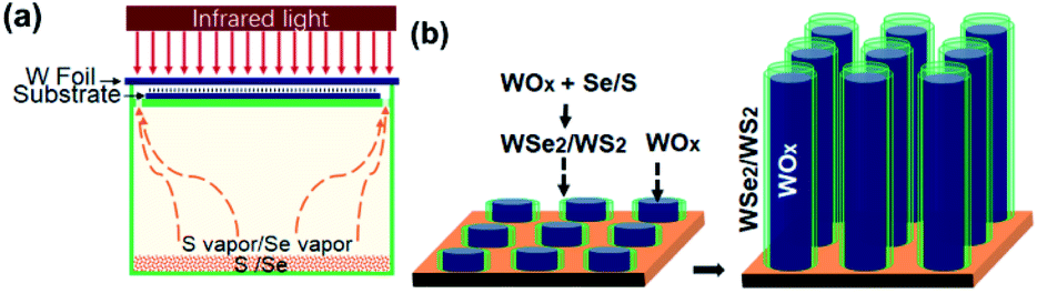 | ||
| Fig. 1 (a) Schematic diagram of infrared-irradiation heating CVD set-up to grow aligned WOx-filled nanotubes. (b) Aligned core–shell co-growth of WOx-filled WSe2/WS2 nanotubes. | ||
Materials characterization
A field-emission scanning electron microscope (SEM, FEI Nova NanoSEM 450) was used to observe the morphology of nanostructure films. Grazing incidence X-ray diffraction (XRD) spectra of the nanostructures were recorded on a Bruker D8-Advance X-ray diffractometer with standard Cu Kα radiation. Raman spectra were recorded using a Horiba Jobin Yvon LabRAM HR-Evolution Raman system with 532 nm laser excitation at room temperature. X-ray photoelectron spectroscopy (XPS, Thermo Scientific Escalab 250Xi) was performed using a monochromatic Al-Kα X-ray source (1486.6 eV), and all binding energies were referenced to that of the neutral C 1s peak. The detailed structures were further characterized via a transmission electron microscope (TEM, JEOL-2100Plus) operated at 200 kV. In the preparation of TEM samples, some nanostructures were stripped off and dispersed in alcohol with the aid of ultrasonic vibration for 10 min, and then a drop of the solution was transferred onto a standard holey-carbon-covered copper grid. Energy-dispersive X-ray spectroscopy (EDS) coupled with SEM or TEM was employed to analyze the chemical compositions of the nanostructures. Two-terminal devices using single sub-oxide nanowires were fabricated on 150 nm SiO2-covered Si substrates via standard electron beam lithography (EBL, performed on a SEM) patterning, sputtering 50 nm-thick Pt as the metal contact, and a subsequent lift-off process. The electrical transport properties were tested on a manual probe station (Cascade EPS150TRIAX system) using a Keysight B1500A semiconductor parameter analyzer.Electrochemical HER measurements
HER electrocatalysis measurements were carried out on an electrochemical workstation (CHI 760E) with a 3-electrode system in a high-purity H2-saturated 0.5 M H2SO4 electrolyte, using a K2SO4 saturated Hg/HgSO4 reference electrode and a graphite counter electrode. Before testing, the reference electrode was calibrated in the same H2-saturated electrolyte with respect to the RHE using Pt plates as the working electrode and counter electrode, and the potential of the reference electrode was measured to be −0.700 V versus RHE. Unless specified, the thin film catalysts were grown using W substrates. Smaller-sized samples (10 mm × 20 mm W substrates) were prepared for HER measurements. To prepare working electrodes, 2/3 of the as-grown film was firstly scratched off from the W substrate, and the remaining film (10 mm × 7 mm, with a geometric area of 0.7 cm2) served as the catalyst. To precisely confine the working area of the catalyst film and exclude any effect from the uncovered W substrate, a thick layer of cured PMMA was used as the sealant and manually coated onto the entire back side and partial front side to only expose the catalyst film window and the contact area (Fig. S4a†). Linear sweep voltammetry (LSV) measurements were performed at a scan rate of 5 mV S−1, and electrochemical impedance spectroscopy (EIS) was carried out by collecting ac impedance spectra from 200 kHz to 0.01 Hz with a voltage perturbation of 10 mV at corresponding open circuit potentials.Results and discussion
The SEM image of the film grown on a Si substrate with feeding Se vapour is displayed in Fig. 2a, showing numerous quasi-aligned 1D nanostructures standing on the substrate. A zoomed-in SEM image in the inset shows their uniform size, diameter of tens of nanometers and length of approximately a couple of micrometers. Using a W foil or Si chip as the substrate, the majority of the as-grown one-dimensional nanostructures were standing vertically on the substrates, but the difference in flatness of the two substrates did cause a slight difference in the overall appearance of the thin films. In comparison, the 1D nanostructures grown on a mirror-polished Si substrate are quite uniformly distributed across the whole substrate (Fig. 2a), while those grown on a W foil substrate have the appearance of a microscopic grass-like meadow with well-distributed micrometer-sized bumps where 1D nanostructures are vertically standing (Fig. S1b†), revealing the original surface roughness and the local topography of W foil. There was no clear difference observed for the size distributions of 1D nanostructures grown on two different substrates. Chemical composition analysis by EDS performed on a SEM detected three elements (W, O and Se) for these nanostructures. The grazing incidence XRD spectrum of the nanostructured film is shown in Fig. 2b, indicating the formation of a hexagonal WSe2 phase (PDF #38-1388) along with monoclinic W18O49 (PDF #05-0392), and the dominant intensity from the (010) plane of W18O49 is in agreement with previously observed aligned growth of W18O49 nanowires along the longitudinal 〈010〉 direction.24 It is worth noting that the 2θ for the (002) basal plane of hexagonal WSe2 peaks at 13.4°, a small left-shift from the 13.62° of the bulk, indicating a slight spacing increase between the (002) basal planes in the formed nanostructures. TEM observations identified that the one-dimensional nanostructures were W18O49-filled WSe2 nanotubes with uncapped bottom-ends and capped top-ends. A TEM image of a filled nanotube (about 2 μm in length and 65 nm in outer diameter) along with high-resolution TEM images taken from three distinct sections of it (bottom/middle/top, highlighted in blue/green/red) is displayed in Fig. 2c, showing that the nanotube shells are capped at the top-end but uncapped at the bottom-end. EDS (performed on a TEM) W/Se/O elemental mapping images recorded on a single nanostructure are displayed in Fig. 2d, revealing its composite structure of WOx core and WSe2 shell. Some representative HRTEM images of individual W18O49-filled WSe2 nanotubes are shown in Fig. 2e. At the top-ends, the oxides are normally not completely filled till the end of the nanotube shell, leaving a short section empty. Most WSe2 nanotubes are capped normally (similar to the one shown at the top-left), but we also observed a few which were capped irregularly, like the one shown at the top-right. At the bottom-ends, uncapped WSe2 shells are normally extended to the very ends of the oxide cores. The (010) plane fringes of single-crystalline monoclinic W18O49 are normal to the (002) basal planes of the WSe2 shell, a clear indication of [010] longitudinal growth for sub-oxide cores. Though most nanotubes were multi-walled (with layer number less than 10) with a (002) basal plane spacing of 0.66 nm, we also observed a few single-walled nanotubes (as the one shown in the middle-right). The nanostructures' Raman spectrum (Fig. S1c†) exhibits characteristic peaks for WSe2, E12g mode at 250 cm−1, 2LA mode at 257 cm−1, and B12g mode at 307 cm−1, consistent with the results reported for WSe2 nanotubes.21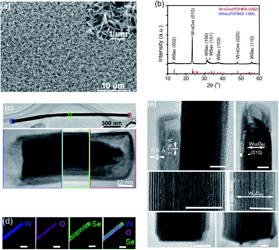 | ||
| Fig. 2 (a) SEM image of the 1D nanostructure film grown on a Si substrate with Se vapor (the inset shows the zoomed-in view), (b) GI-XRD pattern of the nanostructured film grown on a Si substrate (together with PDF reference pattern lines for WSe2 and W18O49), (c) TEM image of a WOx-filled WSe2 nanotube capped at the top-end and its corresponding HRTEM images taken from 3 different sections highlighted in blue/green/red frames, (d) EDS elemental mapping images of an individual one-dimensional nanostructure (scale bars: 50 nm), and (e) HRTEM images of individual W18O49-filled WSe2 capped nanotubes (scale bars: 10 nm). | ||
As described in the Experimental section, to grow WOx-filled WSe2 top-uncapped nanotubes we applied a simple final-stage growth control to skip the final capping step by quickly pumping the chamber down to a pressure below 10 Pa before turning off heating-light to end the CVD growth of WOx-filled WSe2 nanotubes. The TEM observation confirmed that WOx-filled WSe2 nanotubes were successfully uncapped at their top-ends (see Fig. S2† for HRTEM images of uncapped WSe2 nanotubes). Though most nanostructures shared atomic intimacy between oxide cores and dichalcogenides shells, partial filling in the tubular cavity with thinner W18O49 nanowires was also observed. Thus, it is proven that the core–shell co-growth of filled nanotubes can be terminated via removing growth sources (i.e. WOx/WSe2 vapors), which can suddenly freeze the growth at the front-ends and keep the nanotubes uncapped at the top.
Similarly, with the supply of S vapor instead of Se, aligned WOx-filled WS2 nanotubes were uniformly grown on W substrates, and implementing an extra control step at the end of growth, i.e. pumping the chamber down to a pressure below 10 Pa (in a few seconds) before turning off the light heating, also led to the successful synthesis of WS2 uncapped nanotubes. A low-magnification SEM image of the film grown on a W substrate is displayed in Fig. 3a, showing numerous one-dimensional nanostructures with overall orientation roughly vertical to the substrate. The close-up SEM image in the inset shows a similar structure to the above-described WSe2 nanotubes, and these one-dimensional nanostructures are quite uniform in size, tens of nanometers in diameters and also approximately 1–2 micrometers long. Elemental analysis by EDS (performed on a SEM) confirmed the chemical composition of W, O and S elements for these one-dimensional nanostructures (Fig. S3a†). The grazing incidence XRD spectrum of nanostructured films is shown in Fig. 3b, revealing the formation of a 2H-WS2 phase (PDF # 08-237) along with monoclinic W18O49 when the sulfur vapor was introduced. Similarly, the XRD pattern revealed the dominant intensity from the (010) plane of the W18O49 phase, in agreement with its longitudinal 〈010〉 direction within these one-dimensional nanostructures. It is worth noting that the 2θ for the (002) basal plane of 2H-WS2 peaks at 13.9° (a small left-shift from 14.32° for the bulk), consistent with TEM observations of a slight spacing increase between the (002) basal planes in the formed nanostructures. The presence of tungsten sulfide was also verified by XPS. The respective XPS spectra of W 4f and S 2p are shown in Fig. 3c and d, revealing two peaks of W 4f (corresponding to the W4+ state) at binding energies of 33.35 eV and 35.5 eV, and two peaks of S 2p at 163.04 and 164.22 eV, respectively. Another peak at 38.96 eV, corresponding to W6+ oxidation state, is attributed to the presence of W18O49.
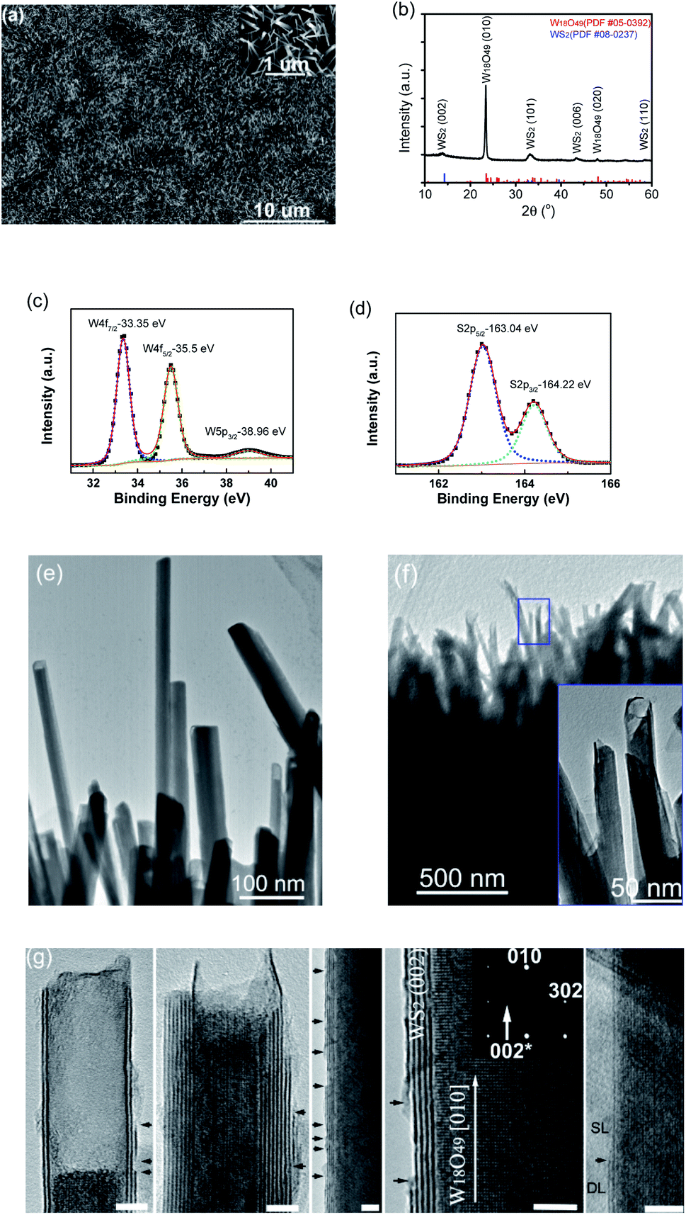 | ||
| Fig. 3 (a) SEM image of the one-dimensional nanostructure film grown on a W substrate with S vapor (the inset shows the high-magnification view), (b) GI-XRD pattern of the film grown on a W substrate (together with PDF reference pattern lines for WS2 and W18O49), (c) and (d) XPS spectra for W and S, (e) TEM image of W18O49-filled WS2 nanotubes with top-ends capped, (f) TEM image of W18O49-filled WS2 nanotubes with top-ends uncapped (the inset shows a closer view of the top-ends highlighted with a blue frame), and (g) representative HRTEM images of individual W18O49-filled open-ended WS2 nanotubes with broken sites at the outermost layer of WS2 shells indicated with black arrows (scale bars: 5 nm). | ||
EDS elemental mapping images of a WOx-filled WS2 nanotube are shown in Fig. S3b,† displaying its composite structure of tungsten oxide inner core and sulfide outer shell. A low-magnification TEM image of WS2 capped nanotubes is shown in Fig. 3e, from which we can see that some are completely filled while others have short sections empty at their top ends. Similar to WSe2 capped nanotubes, WS2 capped nanotubes are capped at the top-ends only but not at the bottom-ends (ESI, see Fig. S3c† for TEM images taken from the bottom/middle/top sections of a single WS2 capped nanotube). It is worth mentioning that this WS2 capped nanotube, unlike the above-described WSe2 nanotubes, bears a distinguishable feature, that is, the outermost wall of the WS2 shell vanishes somewhere along the body, leaving the outermost layer of the WS2 nanotube broken with exposed edges (as indicated with arrows). More HRTEM images of WS2 capped nanotubes are shown in Fig. S3d.† A low-magnification TEM image of WS2 uncapped nanotubes (still assembled in a bundle) is shown in Fig. 3f. The nanostructures are core–shell nanostructures, and these filled nanotubes had survived ultrasonic treatment during TEM sample preparation and were still closely packed and well aligned within this small bundle. A closer observation revealed that all nanotubes were universally not capped at their top-ends (the inset for the zoomed-in image of the blue rectangular framed area). Some representative HRTEM images of individual uncapped nanotubes are shown in Fig. 3g. The (002) layer spacing within WS2 shells is about 0.63 nm, and the layer numbers of outer WS2 nanotubes are typically in the range of 1–10. From the images of oxide cores of nanotubes, it can be seen that the (010) plane fringes of the single-crystalline monoclinic W18O49 nanowire core are aligned normal to the (002) basal planes of the WS2 nanotube shell, which is also consistent with the corresponding selected-area electron diffraction pattern in which the indexed (010) and (302) are from monoclinic W18O49 and weak (002)* from hexagonal WS2. Meanwhile, another remarkably common feature was captured at the outermost layer of WS2 nanotubes where numerous broken sites were present along their bodies (as indicated with arrows in Fig. 3g), which would greatly boost the density of exposed edge sites. For instance, the first nanotube has two layers on the left but three on the right, so its outermost layer is not closed up to form a seamless tubular cylinder, but in the form of broken and curved single-layer nanosheets. Many broken sites can be discerned at the outermost layer of the third nanotube. The nanotube to the right changes from single-layer (SL) to double-layer (DL) at the site indicated with an arrow.
The formation mechanism of the filled nanotubes described here obviously differs from the one for WS2 nanotubes formed through sulfurization of W18O49 nanowire templates, which has been well documented as layer-by-layer inward evolvement to form nested sulfide nanostructures.18,19 The above-described TEM observations would reasonably back up our assumption, a core–shell co-growth vapor–solid process for the formation of filled nanotubes (as illustrated in Fig. 1b), similar to that previously proposed by us for the growth of SiC-filled BN nanotubes.25 At the end of growth, the core–shell co-growth of one-dimensional nanostructures was suddenly terminated via removing the growth sources, leaving WSe2 or WS2 nanotube shells universally uncapped at their top-ends. In the CVD growth of WS2 nanotubes, though the growing tip-ends tend to be favourable deposit fronts for WS2 during the growth, some excessive WS2 could also choose to re-nucleate on the formed shells and grow to form a new SL on the outer wall, and if these newly formed SL nanosheet islands do not come together before the end of growth, ultimately many broken sites are preserved in the outermost layer.
Fig. 4a shows the LSV curves using W-supported five different thin-film working electrodes along with a Pt working electrode and a pure W foil working electrode as controls, respectively. The corresponding uncompensated resistance R was determined by EIS (Fig. 4c). The real potentials applied to the catalysts are iR-corrected, and the currents are normalized to their geometric areas to get the corresponding current densities. The measured η10 are 37, 280/207, 259/156, 370, and 380 mV for Pt, W-supported WSe2 capped-/uncapped-nanotubes, W-supported WS2 capped-/uncapped-nanotubes, W-supported W18O49 nanowires, and W, respectively (see the low-current portions of the LSV curves in Fig. S4b†). Though inferior to Pt, W-supported W18O49-filled tungsten dichalcogenide nanotube catalysts performed much better than the W-supported W18O49 nanowire catalyst and W, due to the significant contributions from tungsten dichalcogenide nanostructures. At high currents, all catalysts showed some fluctuation, mainly due to the desorption process of large-sized hydrogen bubbles. In general, the WS2 catalyst showed better performance than WSe2, and uncapping the nanotubes significantly improved the catalytic activity of their nanotubular catalysts. As demonstrated by other researchers, precise control over the microstructures of nanocatalysts is crucial to optimize HER properties.27–29 In this work, we were able to precisely control the top-capping feature of aligned TMD nanotubes through implementing a simple growth control, which has been proven to be quite effective in improving the catalysis efficacy due to increased active edge sites.
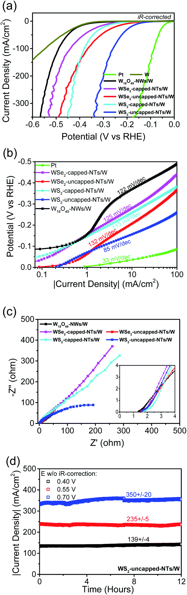 | ||
| Fig. 4 Electrochemical performances of W-supported tungsten dichalcogenide nanotube thin film catalysts for the HER in acid. (a) LSV curves measured on five different W-supported thin film catalysts along with those of Pt and W working electrodes as controls, (b) Tafel plots of different catalysts, (c) EIS Nyquist plots of W-supported thin film catalysts, and (d) stability plots recorded on the W-supported W18O49-filled WS2 uncapped nanotube thin film catalyst at different current levels. | ||
In comparison, the η10 of aligned open-ended W18O49-filled WS2 nanotubes in this work is much lower than those achieved on other MoS2-based nanostructured thin film catalysts,12,13,16,17 and is comparable to the values reported for best-performing nanostructures including single-layer MoSSe nanodots10 and porous graphene supported WS2 nanosheets.11 The electrocatalysis performance comparisons between WS2 uncapped nanotubes in this work and other TMD nanocatalysts that performed excellently are summarized in Table S1 of the ESI.† The corresponding Tafel plots are displayed in Fig. 4b, showing slopes of 113/85 mV per decade for WS2 capped-/uncapped-nanotubes, 125/132 mV per decade for WSe2 capped-/uncapped-nanotubes, and 122 mV per decade for W18O49 nanowires, respectively. Three reactions, the so-called Volmer/Heyrovsky/Tafel step with a Tafel slope of 120/40/30 mV dec−1, respectively, have been identified for the evolvement of the HER in acid.30 The Volmer step is a discharge/adsorption reaction, generating an adsorbed hydrogen atom through reaction between a proton and the transferred electron; the other two steps are H2 desorption reactions, either through combining two H in the Tafel step, or through the reaction between one adsorbed H, one electron and one proton in the Heyrovsky step. The results showed that uncapping the nanotubes did enhance their discharge capability, but relatively high Tafel slopes of WSe2/WS2 nanotubes might be indicating a rate-limiting discharge (Volmer) step for these 1D nanostructure catalysts composed of semiconducting 2H-phases. The Tafel slope of WS2 uncapped nanotubes is comparable to those of other reported WS2 1D nanostructures,20,26 and importantly, has remained relatively constant over a wide span of more than 2 decades or so, indicating a consistent mechanism for its catalytic activities from a low to a high potential range. Fig. 4b also shows another important value, J0, the exchange current density at zero overpotential, an indicator of intrinsic catalytic activity of the catalyst under equilibrium conditions, which is determined to be 0.20 mA cm−2 for WS2 uncapped nanotubes, higher than those obtained from WS2 nanoribbons,26 WSSe nanotubes20 or graphene-supported WS2 nanosheets,11 suggesting a significantly improved electron transfer rate between the proton and the active sites of open-ended WS2 shells of nanotubes with the aid of W18O49 nanowire cores. To evaluate the electrical conduction of W18O49 fillings, we fabricated a two-terminal device with pure W18O49 nanowires via a standard e-beam lithography patterning process. The SEM image of a two-terminal W18O49 nanowire device with Pt contacts is shown in Fig. S5c.† The nanowire channel is 55 nm in diameter and 840 nm in length. It exhibited a symmetric linear IV behaviour, as shown in Fig. S5d,† indicative of the formation of ohmic contacts between the tungsten sub-oxide nanowire and Pt electrodes. A low electric resistivity of 0.07 Ω cm was calculated for this W18O49 nanowire along the longitudinal [010] direction, verifying the highly conductive nature of W18O49 nanowire cores within tungsten dichalcogenide nanotubes.
Seo et al.23 previously demonstrated the positive impact of oxide cores on the HER performance of filled WS2 nanotubes, but the HER performance achieved on the nested WS2 nanotubes (formed through sulfurizing W18O49 nanorods) was far behind those of the highly active WS2/MoS2 nanostructured catalysts. In consideration of the outstanding performance from the aligned W18O49-filled WS2 uncapped nanotube thin film catalyst, several important factors have been reviewed. Firstly, there is direct contact between the W substrate and the bottom-end of highly conductive tungsten sub-oxide cores, so the charge can be easily transferred from substrate to WS2/WSe2 active edge sites along the whole bodies of nanotubes through conducting oxide cores. Secondly, uncapping at top-ends makes all WS2/WSe2 layers of nanotube walls accessible to electrolyte, activating the whole nanotube to be involved in the catalysis, as demonstrated with improved catalytic activity via uncapping nanotubes. Besides, in addition to the contribution from active edge sites at open-ends, the as-grown WS2 nanotubes possess a highly defective outermost layer, which would help maximize active edge sites within this nanostructured catalyst. A simple comparison between a WSe2 uncapped nanotube working electrode and a WS2 uncapped nanotube working electrode is shown in Fig. S4a,† from which we can see much more active edge sites (indicated with arrows) for the latter. It has been pointed out that 1D materials exhibit high surface area and high active-site density, which can facilitate fast charge/mass transport, enable electrolyte to reach deep into the 1D nanostructure forest, and ease the gas release.15 All above-mentioned factors, coupled with the beneficial factors from aligned 1D nanostructures, have contributed together to substantially boost these WS2-based 1D nanostructures to reach their full potential in catalysis.
Fig. 4c displays the EIS Nyquist plots measured on one-dimensional nanostructure thin film electrocatalysts. Their real uncompensated resistances, 1.35 Ω for W18O49 nanowires, 1.59/1.49 Ω for W18O49-filled WSe2 capped-/uncapped-nanotubes, and 1.7/1.55 Ω for W18O49-filled WS2 capped-/uncapped-nanotubes, are pretty low and very comparable. The above results revealed that the addition of few-layer WSe2/WS2 shells did not bring significant real resistance loads on nanotube working electrodes, and opening nanotubes to expose highly conductive W18O49 at their top-ends made it negligible. At their corresponding open circuit potentials, none of the thin-film catalysts formed semicircles, so their charge transfer resistances were not directly obtained. However, the results should allow us to reasonably argue that uncapping nanotubes did significantly lower charge transfer resistances associated with semiconducting tungsten dichalcogenide shells.
Though the results showed that W metal can also catalyze the HER, the contribution from the W substrate to the total catalytic activity of nanostructured thin film catalysts should be negligible because W was covered with densely packed nanotubes/nanowires; meanwhile, in the preparation of nanostructured thin film working electrodes, we sealed the non-film area with PMMA to minimize any effects from W substrates. However, the low resistance of the W substrate played an important role in helping achieve superior performance of WOx-filled WSe2/WS2 nanotube thin film catalysts, which is in agreement with the findings by Chhowalla's group6 that low-resistance contact would help improve good electronic coupling between the substrate and the nanosheet so that TMD basal planes could also contribute to the electrocatalytic activity of the HER. We also tested WSe2 capped nanotubes grown on a highly doped Si substrate as a working electrode for the HER, but its catalytic performance was much worse than that of W-supported ones. As displayed in Fig. S6,† the η10 values are 280 mV and 600 mV for W-supported and Si-supported WSe2 capped nanotubes, respectively. The Si-supported sample's poor electrocatalysis was mainly due to a much higher contact resistance (1.59 Ω for W-supported thin film vs. 29.5 Ω for Si-supported thin film). High-resistance contact was caused by the surface oxidation of the Si substrate to form silicon oxide in the presence of O2 during the CVD process. Therefore, low-resistance contact between catalytic nanotubes and the substrate is crucial to realize the full potential of nanotube catalysts.
In order to evaluate its stability at high current, another crucial factor in the catalyst performances, three different potentials versus RHE, 0.4/0.55/0.7 V without iR compensation, were applied to the WS2 uncapped nanotube working electrode, and the current–time (i–t) behaviours were continuously recorded for 12 hours. Fig. 4d displays the 12 hour stability test results with the corresponding current density range indicated, showing negligible fluctuations (less than 3%) at a current density of 139 mA cm−2 or 235 mA cm−2, and a fluctuation within 6% at a high current density of 350 mA cm−2 over 12 hours, demonstrating its good long-term durability in high current operations. The slightly higher fluctuation at 350 mA cm−2 was mainly caused by the formation of larger-sized hydrogen bubbles at such high currents and a slow desorption process, which affected the actual effective area of the working electrode. After HER stability experiments, we also checked the sample by SEM, and found no obvious physical damage to WS2 nanotubes. The post-HER SEM images of WS2 nanotubes are displayed in Fig. S7,† from which we can see that most nanotubes were still free-standing on the substrate though in slightly worse alignment than the as-grown nanotubes (Fig. 3a), but we also found that some nanotubes have been drawn together to form small solid bundles (as indicated with red arrows) due to long-time e-testing in liquid, possibly as a result of similar liquids' zipping effect observed for single-walled carbon nanotube arrays31 or electrostatic attraction between adjacent neighbor nanotubes. However, this did not cause any degradation to its electrocatalytic performance. We would like to point it out as an advantage of CVD grown thin film type 1D nanostructure arrays over powder type 2D nanosheets, because the irreversible aggregation or accumulation of 2D nanosheets due to the strong van der Waals interactions would greatly decrease their accessible surface area.32
WS2 nanotubes have been an important member of the family of inorganic nanotubes for many years, but unlike in the research of carbon nanotubes, the technique challenge to grow aligned nanotube thin film still remains. The as-grown filled nanotubes were universally uncapped at the top-ends of WS2 shells where the tungsten sub-oxide cores are exposed, so this allowed us to remove exposed oxide fillings by a wet etching method (ESI Fig. S8†). This provides a straight-forward template method to obtain an aligned WSe2/WS2 nanotube film over a large area, which would be of great importance to explore other applications.
Conclusions
In summary, thin films of aligned few-layer WS2 or WSe2 nanotubes in situ filled with highly conductive WOx were successfully synthesized using an infrared-heating CVD process, and a simple growth control was employed to keep the top-ends of nanotubes universally uncapped. An aligned open-ended W18O49-filled WS2 nanotube thin film grown on a W substrate delivered excellent performance to catalyze the HER in acid, including its long-time stability at high currents, high exchange current density of 0.2 mA cm−2, and very low overpotential of 156 mV to drive a current density of 10 mA cm−2. The high-density exposed edge sites existing at the open-ends and the outermost layer of WS2 shells might be a major contributor, but the overall highly efficient catalysis effect could also result from good electronic coupling between the WS2 shells and substrate through highly conductive W18O49 cores. Importantly, the technique used for direct growth of the aligned WOx-filled tungsten dichalcogenide nanotube thin film catalyst over a large area is practical for scale-up production, in consideration of the fact that infrared heating has been applied on a rapid thermal annealing (RTA) 12 inch tool in standard semiconductor process lines. In combination with other beneficial factors associated with 1D nanostructure catalysts,15 the as-synthesized open-ended W18O49-filled WS2 nanotube thin film catalyst was proven to be a very competitive front-runner to achieve highly efficient noble-metal-free catalysis, which promises a bright future for its practical application in water splitting.Conflicts of interest
There are no conflicts to declare.Acknowledgements
Y. L. acknowledges the financial support from the Advanced Talents Incubation Program of Hebei University (521000981204), Hundred Talents Plan of Hebei Province (E2018100001), and Hebei Province Natural Science Fund (A2019201284). W. Z. is thankful for the support from the National Natural Science Foundation of China (11704095).Notes and references
- X. Zou and Y. Zhan, Chem. Soc. Rev., 2015, 44, 5148–5180 RSC.
- N. Han, K. Yang, Z. Lu, Y. Li, W. Xu, T. Gao, Z. Cai, Y. Zhang, V. S. Batista, W. Liu and X. Sun, Nat. Commun., 2018, 9, 924 CrossRef PubMed.
- J. Yang, A. R. Mohmad, Y. Wang, R. Fullon, X. Song, F. Zhao, I. Bozkurt, M. Augustin, E. J. G. Santos, H. S. Shin, W. Zhang, D. Voiry, H. Y. Jeong and M. Chhowalla, Nat. Mater., 2019, 18, 1309–1314 CrossRef CAS PubMed.
- L. Lin, P. Sherrell, Y. Liu, W. Lei, S. Zhang, H. Zhang, G. G. Wallace and J. Chen, Adv. Energy Mater., 2020, 10, 1903870 CrossRef CAS.
- T. F. Jaramillo, K. P. Jørgensen, J. Bonde, J. H. Nielsen, S. Horch and I. Chorkendorff, Science, 2007, 317, 100–102 CrossRef CAS PubMed.
- D. Voiry, R. Fullon, J. Yang, C. Silva, R. Kappera, I. Bozkurt, D. Kaplan, M. J. Lagos, P. E. Batson, G. Gupta, A. D. Mohite, L. Dong, D. Er, V. B. Shenoy, T. Asefa and M. Chhowalla, Nat. Mater., 2016, 15, 1003–1009 CrossRef CAS PubMed.
- C. Wei, R. R. Rao, J. Peng, B. Huang, I. E. L. Stephens, M. Risch, Z. J. Xu and Y. Shao-Horn, Adv. Mater., 2019, 31, 1806296 CrossRef PubMed.
- D. Voiry, H. Yamaguchi, J. Li, R. Silva, D. C. B. Alves, T. Fujita, M. Chen, T. Asefa, V. B. Shenoy, G. Eda and M. Chhowalla, Nat. Mater., 2013, 12, 850–855 CrossRef CAS PubMed.
- J. Yang, D. Voiry, S. J. Ahn, D. Kang, A. Y. Kim, M. Chhowalla and H. S. Shin, Angew. Chem., Int. Ed., 2013, 52, 13751–13754 CrossRef CAS PubMed.
- C. Tan, Z. Luo, A. Chaturvedi, Y. Cai, Y. Du, Y. Gong, Y. Huang, Z. Lai, X. Zhang, L. Zheng, X. Qi, M. Goh, J. Wang, S. Han, X. Wu, L. Gu, C. Kloc and H. Zhang, Adv. Mater., 2018, 30, 1705509 CrossRef PubMed.
- W. Han, Z. Liu, Y. Pan, G. Guo, J. Zou, Y. Xia, Z. Peng, W. Li and A. Dong, Adv. Mater., 2020, 32, 2002584 CrossRef CAS PubMed.
- J. Kibsgaard, Z. Chen, B. N. Reinecke and T. F. Jaramillo, Nat. Mater., 2012, 11, 963–969 CrossRef CAS PubMed.
- Y. Yang, H. Fei, G. Ruan, C. Xiang and J. M. Tour, Adv. Mater., 2014, 26, 8163–8168 CrossRef CAS PubMed.
- N. Lee, Y. Choi, K. Y. Doh, J. Kim, H. Sim, D. Lee, S. Y. Choi and J. K. Kim, J. Mater. Chem. A, 2019, 7, 26378–26384 RSC.
- J. Li and G. Zhen, Adv. Sci., 2017, 4, 1600380 CrossRef PubMed.
- Z. Chen, D. Cummins, B. N. Reinecke, E. Clark, M. K. Sunkara and T. F. Jaramillo, Nano Lett., 2011, 11, 4168–4175 CrossRef CAS PubMed.
- D. Cummins, U. Martinez, A. Sherehiy, R. Kappera, A. Martinez-Garcia, R. K. Schulze, J. Jasinski, J. Zhang, R. K. Gupta, J. Lou, M. Chhowalla, G. Sumanasekera, A. D. Mohite, M. K. Sunkara and G. Gupta, Nat. Commun., 2016, 7, 11857 CrossRef CAS PubMed.
- A. Rothschild, J. Sloan and R. Tenne, J. Am. Chem. Soc., 2000, 122, 5169–5179 CrossRef CAS.
- Y. Q. Zhu, W. K. Hsu, H. Terrones, N. Grobert, B. H. Chang, M. Terrones, B. Q. Wei, H. W. Kroto, D. R. M. Walton, C. B. Boothroyd, I. Kinloch, G. Z. Chen, A. H. Windle and D. J. Fray, J. Mater. Chem., 2000, 10, 2570–2577 RSC.
- K. Xu, F. Wang, Z. Wang, X. Zhan, Q. Wang, Z. Cheng, M. Safdar and J. He, ACS Nano, 2014, 8, 8468–8476 CrossRef CAS PubMed.
- H. Kim, S. J. Yun, J. C. Park, M. H. Park, J. H. Park, K. K. Kim and Y. H. Lee, Small, 2015, 11, 2192–2199 CrossRef CAS PubMed.
- Y. Chen, Y. Li, Y. Wang, T. Tian and L. C. Qin, Mater. Res. Lett., 2017, 5, 508–515 CrossRef CAS.
- B. Seo, H. Y. Jeong, S. Y. Hong, A. Zak and S. H. Joo, Chem. Commun., 2015, 51, 8334–8337 RSC.
- Y. Li, Y. Bando and D. Golberg, Adv. Mater., 2003, 15, 1294–1296 CrossRef CAS.
- Y. Li, P. S. Dorozhkin, Y. Bando and D. Golberg, Adv. Mater., 2005, 17, 545–549 CrossRef CAS.
- J. Lin, Z. Peng, G. Wang, D. Zakhidov, E. Larios, M. J. Yacaman and J. M. Tour, Adv. Energy Mater., 2014, 4, 1301875 CrossRef.
- Y. Li, C. Gao, W. Jiang, C. Zhuang, W. Tan, W. Li, Y. Li, L. Wang, X. Liao, Z. Sun, J. Zou and X. Han, Appl. Catal., B, 2021, 286, 119923 CrossRef CAS.
- C. Gao, C. Zhuang, Y. Li, H. Qi, G. Chen, Z. Sun, J. Zou and X. Han, J. Mater. Chem. A, 2021, 9, 13056 RSC.
- C. Zhuang, H. Qi, X. Cheng, G. Chen, C. Gao, L. Wang, S. Sun, J. Zou and X. Han, Angew. Chem., Int. Ed., 2019, 58, 18627–18633 CrossRef CAS PubMed.
- B. E. Conway and B. V. Tilak, Electrochim. Acta, 2002, 47, 3571–3594 CrossRef CAS.
- D. N. Futaba, K. Hata, T. Yamada, T. Hiraoka, Y. Hayamizu, Y. Kakudate, O. Tanaike, H. Hatori, M. Yumura and S. Iijima, Nat. Mater., 2006, 5, 987–994 CrossRef CAS PubMed.
- J. Shen, Y. Zhu, H. Jiang and C. Li, Nano Today, 2016, 11, 483–520 CrossRef CAS.
Footnote |
| † Electronic supplementary information (ESI) available. See DOI: 10.1039/d1na00571e |
| This journal is © The Royal Society of Chemistry 2021 |