
 Open Access Article
 This Open Access Article is licensed under a Creative Commons Attribution-Non Commercial 3.0 Unported Licence
Anomalously polarised emission from a MoS2/WS2 heterostructure†
P. Riya
Mol
,
Prahalad Kanti
Barman
 ,
Prasad V.
Sarma
,
Abhishek S.
Kumar
,
Satyam
Sahu
,
Manikoth M.
Shaijumon
and
Rajeev N.
Kini
*
,
Prasad V.
Sarma
,
Abhishek S.
Kumar
,
Satyam
Sahu
,
Manikoth M.
Shaijumon
and
Rajeev N.
Kini
*
Indian Institute of Science Education and Research Thiruvananthapuram (IISER TVM), Maruthamala P. O. Vithura, Kerala 695551, India. E-mail: rajeevkini@iisertvm.ac.in
First published on 17th August 2021
Abstract
We report circularly polarised emission, with helicity opposite to the optical excitation, from a van der Waals heterostructure (HS) consisting of a monolayer MoS2 and three-layer WS2. Selective excitation of the MoS2 layer confirms that this cross-polarized emission is due to the charge transfer from the WS2 layers to the MoS2 layer. We propose that the high levels of n-doping in the constituent layers due to sulphur vacancies and defects give rise to an enhanced transition rate of electrons from the k valley of WS2 to the k′ valley of MoS2, which leads to the emission, counter polarized to the excitation. Simulations based on the rate equation model support this conclusion.
1. Introduction
Two-dimensional van der Waals heterostructures (HSs) made up of atomically thin layers of transition metal dichalcogenides (TMDs) have emerged as a platform for exploring spin and valley physics and its applications.1,2 Many of these HSs have a type II band alignment, leading to efficient and ultrafast separation of the photoexcited electrons and holes into the different layers.3–5 This makes the HSs particularly interesting for light-harvesting applications. In HSs, the electrons and holes are separated in both the real and the momentum space, giving rise to a long valley lifetime.6–8 Hence, TMD HSs are promising also for valleytronics applications. The separation of the charges in different layers gives rise to interlayer excitons (IXs).9–12 There have been extensive studies focussing on the IXs9–12 as well as intralayer excitons.3,13The HSs inherit the interesting spin–valley physics of the constituent layers and lead to numerous intriguing phenomena. Due to the large spin–orbit coupling and entangled spin and valley degrees of freedom (DoF), TMDs provide a unique platform to manipulate valley pseudospin through circularly polarized light.14,15 Due to the valley contrasting Berry curvature and magnetic moment, the valley DoF can be manipulated using a magnetic field.16–19 Additionally, the valley splitting can be enhanced by more than an order of magnitude by taking advantage of antiferromagnetic substrates' magnetic proximity coupling.20 Doping provides another exotic way to control the exchange interactions in TMDs, leading to giant and tunable valley splitting in TMDs. TMDs grown by the chemical vapour deposition (CVD) method have a high density of chalcogen vacancies. In HSs with type-II band alignment, the electrons and holes get localized in different layers via ultrafast charge transfer.3 It has been shown that this leads to a dramatic enhancement in the exchange interaction along with an anomalous enhancement in the g-factor.13 The ultrafast charge transfer in TMD HSs also provides an all-optical route to control spin–valley phenomena by tuning the doping concentration by varying the laser power.13
Another interesting feature of TMDs, due to the valley-degenerate spin-contrasting bandstructure, is that they host both optically active and inactive intravalley excitons, called bright and dark excitons, respectively.21–24 In Mo-based monolayer TMDs, the ground state is a bright exciton, and the dark state lies energetically above it. Though most of the studies on TMDs focused on bright excitons, the existence of dark excitons has been experimentally probed via different techniques.25–27 Dark excitons are highly interesting, and many of the optical properties strongly depend on the competition between the bright and dark exciton states. Experiments have shown that the application of a magnetic field can brighten the dark exciton states.26–30 Plasmon induced brightening of dark excitons in the TMDC monolayer has also been reported.31 In doped TMD layers, trions (charged excitons) are also formed along with excitons. The application of a magnetic field has been shown to brighten the corresponding dark (charged) excitons.28 Intriguingly, the emission from the brightened dark exciton states showed helicity opposite to that of the excitation.28 However, in TMD HSs, even though IXs with helicity opposite to the excitation have been reported, reversing the helicity of intralayer exciton emission has not been reported, and intralayer excitons preserve the helicity of the excitation light. We report circularly polarised intralayer exciton emission, with helicity opposite to the optical excitation, from a MoS2/WS2 heterostructure. Selective excitation of the MoS2 layer confirms that this cross-polarized emission is due to the charge transfer from the WS2 layers to the MoS2 layer. We propose that a dark exciton state in the MoS2 layer gets brightened due to n-doping, and the anomalous polarization arises due to the charge transfer from the conduction band of WS2 to this brightened dark exciton state. We provide simulations based on the rate equation model to support this conclusion.
2. Sample growth and characterisation
The WS2/MoS2 HS was synthesised on a Si/SiO2 substrate via single-step chemical vapour deposition (CVD) at 900 °C using a Thermo Scientific Lindberg Blue M split-tube furnace. First, WO3 powder (Aldrich puriss 99.9%) is dispersed in ethanol (0.2 mg mL−1), and 10 μL dispersion is drop coated to each cleaned substrate. Similarly, MoO3 powder is dispersed in ethanol at a similar concentration. After drying the WO3 dispersion, 10 μL of MoO3 dispersion is drop coated on the same substrate. Once dried in air, these substrates were loaded at the centre of the tubular furnace. As the sulfur source, 500 mg sulfur powder (Aldrich, purum 99.5%) is placed at the upstream end of the tube, just outside the heating elements. The tube is flushed several times using ultra-high-pure argon gas before the deposition to remove moisture/oxygen from the furnace. The heterostructure growth was observed at a temperature of 900 °C after a dwell time of 10 minutes while maintaining 200 sccm argon flow throughout the experiment.Temperature-dependent and helicity resolved photoluminescence (PL) was performed using a homebuilt micro-PL setup in the backscattering configuration. For PL measurements, a 532 nm solid-state laser with an average laser power of 3.5 mW was used as the excitation source. The excitation light was focused on the sample using a 10× objective lens (NA = 0.24) which gave a spot size of ≈3 μm-diameter. The signals were collected with the same objective lens, analysed using a 0.32 m monochromator (Horiba-Jobin Yvon iHR320) and detected with a thermoelectrically cooled CCD camera. The experiments were performed at different temperatures in the range of 16–300 K using an ultralow vibration closed-cycle refrigerator. The PL and Raman maps were obtained using a Raman microscope (XploRa PLUS, Horiba Scientific) with 532 nm laser excitation. A 50× microscope objective (NA = 0.8) was used, and it gave a spot size of ≈1 μm-diameter on the sample during PL mapping.
An atomic force microscope (AFM) image of the HS is shown in Fig. 1(a). The sample has a three-layer (3L) thick hexagonal base (WS2) with a triangular monolayer (ML) on top of it (MoS2), as indicated by the dotted lines in Fig. 1(a). The thickness of the WS2 and MoS2 layers is confirmed using AFM line scans, as shown in the inset of Fig. 1(a). It has been reported earlier that in WS2, compared to ML, even though the emission is weaker in thicker flakes, thicker flakes give rise to a higher degree of polarization.32,33 Hence we have chosen a 3L thick WS2 to form the HS. The top panel of Fig. 1(b) shows the PL from the triangular heterostructure region, which is similar to what has been reported earlier.3,12,13,34 The PL spectra obtained from a CVD grown ML-MoS2 and a 3L-WS2 is also shown in Fig. 1(b) for reference. The PL spectra from HS show two peaks, an intense peak close to the charged exciton peak (AX−) in MoS2 (XM) and a second peak at higher energy (XW). The dominant peak XM near the MoS2 AX− peak indicates that the HS is highly doped, and the peak position agrees with the previous reports on unintentionally doped MoS2/WS2 HS.13,35 The XW peak is close to the emission peak observed in 3L-WS2 and the B-exciton (BX) in ML-MoS2. It has been reported that the PL from the HS is an additive spectrum of emission from the constituent WS2 and MoS2 layers in the ratio 1![[thin space (1/6-em)]](https://www.rsc.org/images/entities/char_2009.gif) :5–10.5,34 We believe that the XW consists of contributions from both the exciton emission of WS2 and the BX emission of MoS2. In this paper, we focus on the XM emission peak. Fig. 1(c) and (d) show the 2D map of the emission intensity near XM and XW. It can be seen that the emission from the triangular heterostructure region has a peak near XM, and the XW emission is observed from the whole sample, including the 3L-WS2 base. The Raman and PL intensity maps confirm that the MoS2 layer is present only in the triangular region, as indicated in Fig. 1(a).
:5–10.5,34 We believe that the XW consists of contributions from both the exciton emission of WS2 and the BX emission of MoS2. In this paper, we focus on the XM emission peak. Fig. 1(c) and (d) show the 2D map of the emission intensity near XM and XW. It can be seen that the emission from the triangular heterostructure region has a peak near XM, and the XW emission is observed from the whole sample, including the 3L-WS2 base. The Raman and PL intensity maps confirm that the MoS2 layer is present only in the triangular region, as indicated in Fig. 1(a).
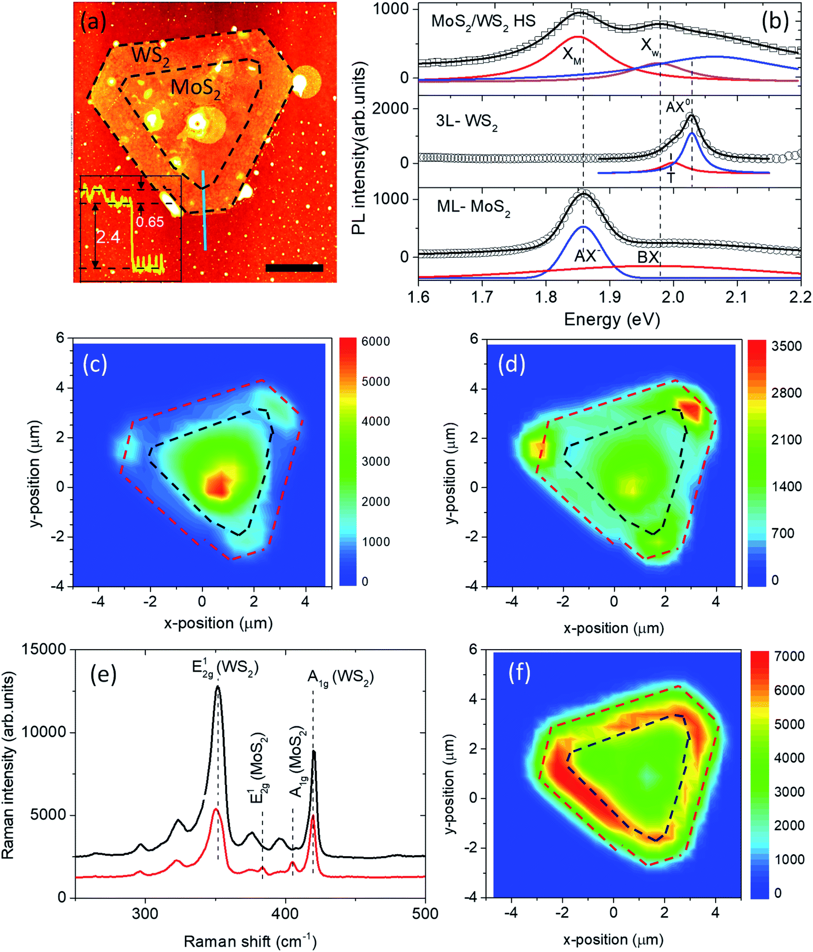 | ||
| Fig. 1 (a) Atomic force microscope image of the MoS2/WS2 heterostructure (HS). The dashed lines indicate the boundary of the constituent WS2 and MoS2 layers. The scale bar is 2 microns. Inset shows the line profile along an edge of the sample indicated by the grey line (b) low temperature (T = 17 K) PL spectra from MoS2/WS2 HS (top panel), 3L-WS2 (middle panel) and ML-MoS2 (bottom panel) obtained using 532 nm, linearly polarized excitation. The open symbols are the experimental data; the solid black lines are obtained by fitting the peaks to Lorentzian. The red, blue and pink lines represent the individual Lorentzian peaks. The data and the Lorentzian peaks are offset vertically for clarity. PL intensity map of (c) XM and (d) XW peaks in the HS sample. (e) Raman signal from the top (red) and edge (black) of the HS sample. (f) Raman intensity map of the A1g peak of the HS sample. | ||
Fig. 1(e) shows the Raman signals from the top of the heterostructure and the edge of the sample. The Raman signal from the top of the heterostructure consists of peaks corresponding to the in-plane (E12g) and out-of-plane (A1g) modes of MoS2 and WS2. The Raman signal from the edge of the sample shows only (E12g) and (A1g) modes corresponding to the WS2 layer, confirming that the hexagonal base consists of WS2, and MoS2 is present only in the triangular region. Apart from the E12g and A1g modes, there are two other modes, marked U1 and U2 in ESI Fig. S1,† which appear both in the heterostructure region and the edge of the sample. However, their origin is not clear at this point. Fig. 1(f) shows the 2D map of the A1g mode of WS2. In the triangular HS region, A1g of WS2 shows a slight decrease in intensity due to the presence of the MoS2 layer. Hence, we confirm that the heterostructure consists of a hexagonal 3L-WS2 with a triangular ML-MoS2 on top of it.
3. Results and discussion
We studied the polarisation characteristics of the emission from the HS. The HS was excited with a circularly polarised laser at 532 nm, and the polarisation of the PL emission was analysed. Fig. 2(a) shows the PL emission from the heterostructure at room temperature and low temperature (≈16 K) upon excitation with right-circularly polarised light (σ+). At room temperature, the XW peak is predominantly co-polarised (σ+) with the excitation, while the XM is cross-polarised (σ−) with the excitation. The peaks are blue-shifted at low temperature; however, similar polarisation dependence is observed; the XM peak is cross-polarised (σ−), and the XW peak is co-polarised (σ+) with the excitation. Again same polarization characteristics were observed upon excitation with left-circularly polarised light (σ−), as shown in ESI Fig. S1.†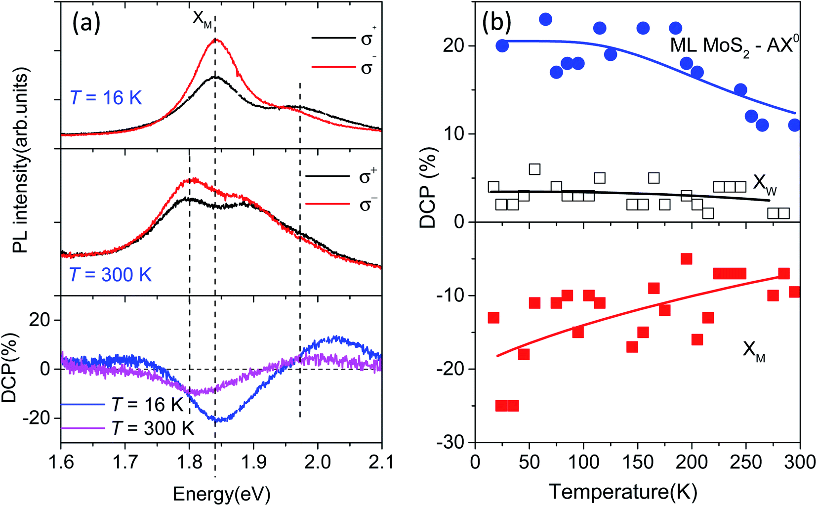 | ||
| Fig. 2 (a) Helicity resolved PL spectra obtained from the MoS2/WS2 HS with 532 nm, circularly polarized (σ+) excitation at T = 16 K (top panel) and T = 300 K (middle panel). Degree of polarization (DCP) at T = 16 K and T = 300 K (bottom panel) obtained with 532 nm, σ+ excitation of the MoS2/WS2 HS. (b) DCP near the XM and XW peaks, at different temperatures, obtained with 532 nm, σ+ excitation of the MoS2/WS2 HS. The DCP data corresponding to the charged exciton (AX−) in ML-MoS2 are also shown in the top panel. The solid lines are a guide for the eye. | ||
We define the degree of circular polarisation (DCP) as ρ = (I+ − I−)/(I+ + I−), where I+ (I−) denotes the intensity of the PL component co-polarized (cross-polarized) with the excitation. DCP is plotted in the bottom panel of Fig. 2(a), and it can be seen that the DCP is negative near XM. Similar measurements were performed on individual ML MoS2 and 3L WS2 flakes, shown in supplementary Fig. S2.† The ML MoS2 and the 3L WS2 flakes do not show this anomalous counter polarisation for the emission, which agree with earlier reports.14,32,36–38Fig. 2(b) shows the temperature dependence of the DCP near XM and XW peaks. For reference, the temperature dependence of the DCP of AX− emission from ML-MoS2 is also shown in Fig. 2(b). It can be seen that the DCP near the XW peak in the HS at all temperatures, even though very low (≈1–4%), remains positive, and the DCP remains negative for the XM peak. DCP measurements have been reported earlier on MoS2/WS2 HSs, and interlayer excitons have been shown to have negative DCP.10,11,13 However, intralayer exciton emission has not been reported to show negative DCP.10,13 Most of the earlier work was reported on HSs comprising of MLs of MoS2 and WS2.3,12,13,34 Hence, we first look at the possibility of the negative DCP to be due to the different layer structure used here, i.e., 3L-WS2 and ML-MoS2.
Even though density functional theory (DFT) often underestimates the bandgap, it can provide necessary information for distinguishing different excitations in different heterostructures. We computed the bandstructure of the HS consisting of 3L-WS2 and ML-MoS2 using DFT (see ESI Note 1† for details) and compared it with the bandstructure of the well-studied HS comprising MLs of MoS2 and WS2 in ESI Fig. S3.† The band structure calculations demonstrate type-II band alignment.4,5 Compared to the HS with ML-WS2, for the HS with 3L-WS2, the band minimum at the Q-point is further lowered, and the VB maximum at the Γ-point is further pushed up.12,13,34 Hence the IX is at much lower energy than what has been observed in the literature and is beyond the spectral range accessible in our measurements. However, the band minima near K-points are very similar in both the HSs. Hence, the difference in the polarization behaviour of XM emission cannot be attributed to the changes in the band structure.
We first conducted measurements with a 633 nm (1.96 eV) laser excitation to understand the origin of this cross-polarised emission. 633 nm laser allowed us to selectively excite the MoS2 layer in the HS and ensure that the WS2 layers were not populated. The helicity resolved PL and DCP from the HS at 17 K with 633 nm, σ+ polarized excitation is shown in Fig. 3. It can be seen that with 633 nm excitation, the DCP of the XM peak is positive. Similar behaviour was obtained with σ− polarized 633 nm excitation as shown in ESI Fig. S4(a).† Positive DCP was obtained for all temperatures up to room temperature, with 633 nm excitation as shown in ESI Fig. S4(b).† The absence of negative DCP when WS2 is not populated confirms that the negative DCP arises from the transfer of electrons from the WS2 layer to the MoS2 layer.
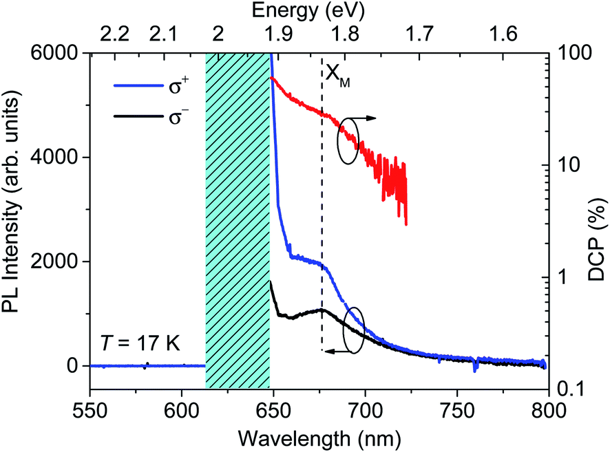 | ||
| Fig. 3 Helicity resolved PL spectra and degree of polarization (DCP) obtained from the MoS2/WS2 HS with 633 nm, circularly polarized (σ+) excitation at T = 17 K. The shaded blue region indicates the stopband of the filter used to block the laser light from reaching the detector. | ||
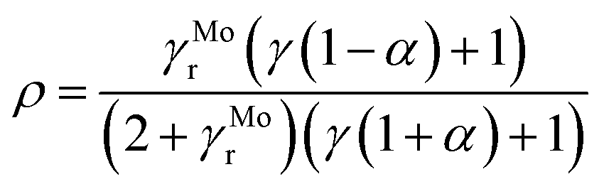
After the excitation of the HS layers, charge transfer occurs, mostly via spin-conserving transfers to the lowest energy band, irrespective of the interlayer momentum mismatch.10 So the excitation of the WS2 layer with σ+ polarized light and subsequent charge transfer could lead to the population of the spin-up state in the k valley of MoS2, which would result in the emission of σ+ polarized light. However, negative DCP results from the dominant emission of σ− polarized light. Negative DCP indicates that interlayer scattering results in the enhanced exciton population in the k′ valley of MoS2, which would give rise to the emission of σ− polarized light. To examine this possibility, we use a rate equation model as described below. A schematic of the band structure and the spin configuration is shown in Fig. 4(a). The system of rate equations for the WS2/MoS2 HS can be written as follows:
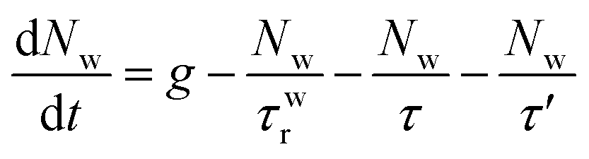
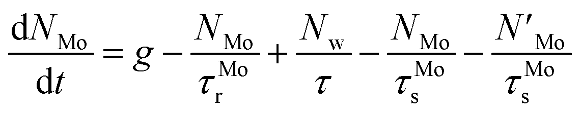
NMo
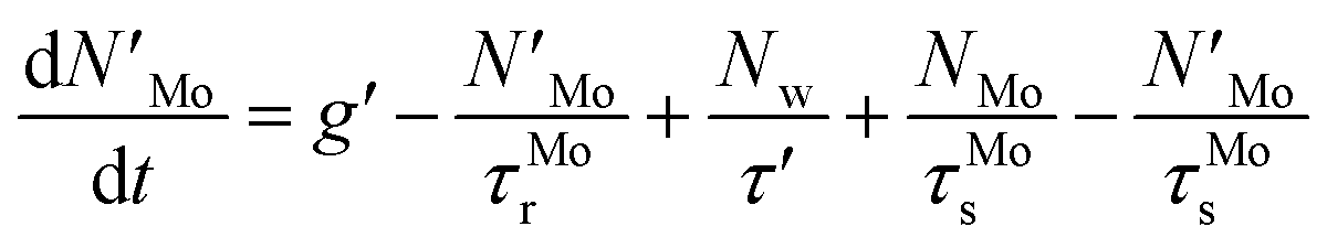
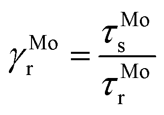
 is the exciton population in the k (k′) valley of the MoS2 layer and Nw the exciton population in the k valley of the WS2 layer. g (g′) is the generation rate in the k (k′) valley, which is assumed to be a constant for continuous-wave excitation. We assumed that σ+ excitation generates excitons in the k valleys of MoS2 and WS2 layers, and for simplicity, we have ignored the scattering of electrons to the k′ valley of the WS2 layer. This assumption is valid since, due to the type-II band alignment, the transfer of photogenerated electrons from the WS2k valley to the MoS2 valleys is more efficient than their scattering to the k′ valley of the WS2.39τMos and τMor represent the intervalley scattering time and the radiative recombination time, respectively, in the MoS2 layer. τwr represents the radiative recombination time in the WS2 layer. τ (τ′) represents the intralayer scattering time between the k valley in WS2 and the k (k′) valley in MoS2. The polarization state is calculated under steady-state conditions
 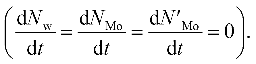 . The DCP of the XM emission is related to the population of exciton states in the k (k′) valleys of MoS2,
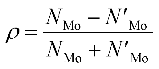
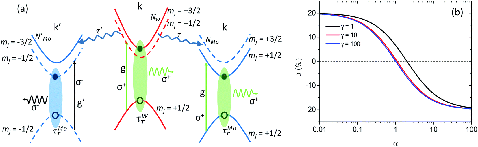 | ||
| Fig. 4 (a) A schematic of the different bands in the MoS2/WS2 HS. Solid and dotted lines represent bands with different spin configurations. The bands are labelled with the z-component of their total angular momentum, mj. Vertical arrows indicate optical excitations: black and green arrows correspond to σ− and σ+ excitation, respectively. The black and green wiggly arrows indicate σ− and σ+ emission, respectively. The gray wiggly arrows represent spin-conserving interlayer transfer to the lowest energy band. (b) Degree of circular polarization, ρ, calculated using the rate equation model described in the main text for γMor = 1/2 and different values of α. | ||
Solving the above set of rate equations for g = 1 and g′ = 0 we obtain
 and
and 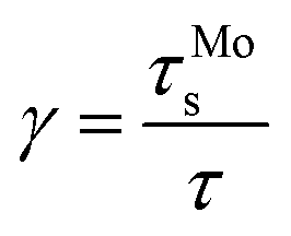 represent the relaxation rates and
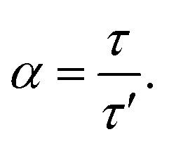
If we ignore the interlayer scattering (γ = 0), the above equation describes an isolated MoS2 layer, and it reduces to 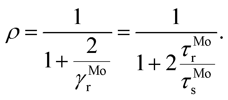 40 In that case, we obtain ρ ≈ 20% for γMor ≈ 1/2, which agrees with the ρ obtained for ML-MoS2 at low temperature. τMo/Wr is in the range of picoseconds to hundreds of picoseconds.25,41,42 The intervalley scattering time τMos depends on the excitation energy but will be of the same order of τMo/Wr.40 It has been shown that the interlayer scattering time (τ′, τ) is of the order of 50–450 fs (ref. 3, 34, 43 and 44) which means γ, γ′ > 1. Fig. 4(b) shows ρ as a function of α for γMor = 1/2 and for different values of γ, which shows that negative DCP is indeed possible for τ′ < τ. This means that electrons photoexcited to the k valley of WS2 by σ+ polarised light are scattered preferentially to the k′ valley compared to the k valley of MoS2. We believe that this is due to unintentional doping of the HS. CVD grown samples have a high density of sulphur vacancies, leading to high levels of n-doping which is evident from the emission XM near the charged exciton energy in MoS2.13 The high levels of n-doping has two effects. Firstly, the Fermi level will be located in the spin-split upper conduction band of MoS2.13 Because of this, the electrons from WS2 layers will be scattered to the spin-split upper conduction bands of MoS2. The transition to the spin-split upper conduction band of MoS2k′ valley (mj = −3/2) would be a spin-conserving transition. Hence, possibly, the transition rate of this spin-conserving transition is enhanced compared to the spin-flip transition to the k valley (mj = +3/2). Normally, the spin-conserving transition from WS2 to the spin-split upper conduction band of the MoS2k′ valley would give rise to dark (neutral or charged) excitons. However, as another consequence of the n-doping of the layers the dark exciton state is brightened, similar to the brightening observed earlier for the dark IX state in MoS2/WS2 HSs due to electrostatic doping.9
4. Conclusions
In conclusion, we unveil anomalous polarization from a van der Waals heterostructure (HS) consisting of ML-MoS2 and 3L-WS2. Selective excitation of the MoS2 layer in the HS demonstrates that this anomalous polarization originates from the charge transfer from WS2 to MoS2 layers. We propose that due to high levels of n-doping in the layers, caused by sulphur vacancies and defects, the transition rate of electrons from the k valley of WS2 to the k′ valley of MoS2 is enhanced, which leads to emission, counter polarized (σ−) to the excitation (σ+). We simulated this scenario using a set of coupled rate equations, and the simulations agree well with our experimental observations. Our measurements provide new prospects to control the helicity of the emission from van der Waals HSs via doping.Author contributions
PRM and PKB did the measurements and analysed the data. PVS grew the samples. ASK did the DFT calculations. SS did the simulations based on the rate equation model. MMS designed and supervised the growth of nanostructures. RNK supervised the measurements & analysis and prepared the manuscript with inputs from all co-authors.Conflicts of interest
The authors declare that they have no known competing financial interests or personal relationships that could have appeared to influence the work reported in this paper.Acknowledgements
RNK acknowledges the funding support by the Science and Engineering Research Board, Department of Science and Technology, India, through the Research Grant No. CRG/2019/004865 and IPA/2020/000021. The support for computing time at the IISER Thiruvananthapuram HPC cluster “Padmanabha” is also kindly acknowledged.References
- A. K. Geim and I. V. Grigorieva, Van der Waals heterostructures, Nature, 2013, 499, 419–425 CrossRef CAS PubMed.
- P. Rivera, H. Yu, K. L. Seyler, N. P. Wilson, W. Yao and X. Xu, Interlayer valley excitons in heterobilayers of transition metal dichalcogenides, Nat. Nanotechnol., 2018, 13, 1004–1015 CrossRef CAS PubMed.
- X. Hong, J. Kim, S. F. Shi, Y. Zhang, C. Jin, Y. Sun, S. Tongay, J. Wu, Y. Zhang and F. Wang, Ultrafast charge transfer in atomically thin MoS2/WS2 heterostructures, Nat. Nanotechnol., 2014, 9, 682–686 CrossRef CAS PubMed.
- J. Kang, S. Tongay, J. Zhou, J. Li and J. Wu, Band offsets and heterostructures of two-dimensional semiconductors, Appl. Phys. Lett., 2013, 102, 12111 CrossRef.
- H. P. Komsa and A. V. Krasheninnikov, Electronic structures and optical properties of realistic transition metal dichalcogenide heterostructures from first principles, Phys. Rev. B: Condens. Matter Mater. Phys., 2013, 88, 085318 CrossRef.
- J. Kim, C. Jin, B. Chen, H. Cai, T. Zhao, P. Lee, S. Kahn, K. Watanabe, T. Taniguchi, S. Tongay, M. F. Crommie and F. Wang, Observation of ultralong valley lifetime in WSe2/MoS2 heterostructures, Sci. Adv., 2017, 3, e1700518 CrossRef PubMed.
- C. Jin, J. Kim, M. Iqbal Bakti Utama, E. C. Regan, H. Kleemann, H. Cai, Y. Shen, M. J. Shinner, A. Sengupta, K. Watanabe, T. Taniguchi, S. Tongay, A. Zettl and F. Wang, Imaging of pure spin-valley diffusion current in WS2-WSe2 heterostructures, Science, 2018, 360, 893–896 CrossRef CAS PubMed.
- P. Rivera, K. L. Seyler, H. Yu, J. R. Schaibley, J. Yan, D. G. Mandrus, W. Yao and X. Xu, Valley-polarized exciton dynamics in a 2D semiconductor heterostructure, Science, 2016, 351, 688–691 CrossRef CAS PubMed.
- A. Ciarrocchi, D. Unuchek, A. Avsar, K. Watanabe, T. Taniguchi and A. Kis, Polarization switching and electrical control of interlayer excitons in two-dimensional van der Waals heterostructures, Nat. Photonics, 2019, 13, 131–136 CrossRef CAS PubMed.
- W. T. Hsu, L. S. Lu, P. H. Wu, M. H. Lee, P. J. Chen, P. Y. Wu, Y. C. Chou, H. T. Jeng, L. J. Li, M. W. Chu and W. H. Chang, Negative circular polarization emissions from WSe2/MoSe2 commensurate heterobilayers, Nat. Commun., 2018, 9, 1356 CrossRef PubMed.
- A. T. Hanbicki, H. J. Chuang, M. R. Rosenberger, C. S. Hellberg, S. V. Sivaram, K. M. McCreary, I. I. Mazin and B. T. Jonker, Double Indirect Interlayer Exciton in a MoSe2/WSe2 van der Waals Heterostructure, ACS Nano, 2018, 12, 4719–4726 CrossRef CAS PubMed.
- M. Okada, A. Kutana, Y. Kureishi, Y. Kobayashi, Y. Saito, T. Saito, K. Watanabe, T. Taniguchi, S. Gupta, Y. Miyata, B. I. Yakobson, H. Shinohara and R. Kitaura, Direct and Indirect Interlayer Excitons in a van der Waals Heterostructure of hBN/WS2/MoS2/hBN, ACS Nano, 2018, 12, 2498–2505 CrossRef CAS PubMed.
- J. Zhang, L. Du, S. Feng, R. W. Zhang, B. Cao, C. Zou, Y. Chen, M. Liao, B. Zhang, S. A. Yang, G. Zhang and T. Yu, Enhancing and controlling valley magnetic response in MoS2/WS2 heterostructures by all-optical route, Nat. Commun., 2019, 10, 4226 CrossRef PubMed.
- K. F. Mak, K. He, J. Shan and T. F. Heinz, Control of valley polarization in monolayer MoS2 by optical helicity, Nat. Nanotechnol., 2012, 7, 494–498 CrossRef CAS PubMed.
- H. Zeng, J. Dai, W. Yao, D. Xiao and X. Cui, Valley polarization in MoS2 monolayers by optical pumping, Nat. Nanotechnol., 2012, 7, 490–493 CrossRef CAS PubMed.
- Y. Li, J. Ludwig, T. Low, A. Chernikov, X. Cui, G. Arefe, Y. D. Kim, A. M. Van Der Zande, A. Rigosi, H. M. Hill, S. H. Kim, J. Hone, Z. Li, D. Smirnov and T. F. Heinz, Valley splitting and polarization by the Zeeman effect in monolayer MoSe2, Phys. Rev. Lett., 2014, 113, 1–5 Search PubMed.
- A. Srivastava, M. Sidler, A. V. Allain, D. S. Lembke, A. Kis and A. Imamoğlu, Valley Zeeman effect in elementary optical excitations of monolayer WSe2, Nat. Phys., 2015, 11, 141–147 Search PubMed.
- G. Aivazian, Z. Gong, A. M. Jones, R. L. Chu, J. Yan, D. G. Mandrus, C. Zhang, D. Cobden, W. Yao and X. Xu, Magnetic control of valley pseudospin in monolayer WSe2, Nat. Phys., 2015, 11, 148–152 Search PubMed.
- D. Macneill, C. Heikes, K. F. Mak, Z. Anderson, A. Kormányos, V. Zólyomi, J. Park and D. C. Ralph, Breaking of valley degeneracy by magnetic field in monolayer MoSe2, Phys. Rev. Lett., 2015, 114, 1–5 CrossRef PubMed.
- L. Xu, M. Yang, L. Shen, J. Zhou, T. Zhu and Y. P. Feng, Large valley splitting in monolayer WS2 by proximity coupling to an insulating antiferromagnetic substrate, Phys. Rev. B, 2018, 97, 2–7 Search PubMed.
- H. Yu, G. B. Liu, P. Gong, X. Xu and W. Yao, Dirac cones and Dirac saddle points of bright excitons in monolayer transition metal dichalcogenides, Nat. Commun., 2014, 5, 1–7 Search PubMed.
- H. Yu, X. Cui, X. Xu and W. Yao, Valley excitons in two-dimensional semiconductors, Natl. Sci. Rev., 2015, 2, 57–70 CrossRef CAS.
- C. Robert, D. Lagarde, F. Cadiz, G. Wang, B. Lassagne, T. Amand, A. Balocchi, P. Renucci, S. Tongay, B. Urbaszek and X. Marie, Exciton radiative lifetime in transition metal dichalcogenide monolayers, Phys. Rev. B, 2016, 93, 1–10 CrossRef.
- G. Berghäuser, P. Steinleitner, P. Merkl, R. Huber, A. Knorr and E. Malic, Mapping of the dark exciton landscape in transition metal dichalcogenides, Phys. Rev. B, 2018, 98, 1–6 CrossRef.
- X. X. Zhang, Y. You, S. Y. F. Zhao and T. F. Heinz, Experimental Evidence for Dark Excitons in Monolayer WSe2, Phys. Rev. Lett., 2015, 115, 1–6 Search PubMed.
- Z. Li, T. Wang, C. Jin, Z. Lu, Z. Lian, Y. Meng, M. Blei, S. Gao, T. Taniguchi, K. Watanabe, T. Ren, S. Tongay, L. Yang, D. Smirnov, T. Cao and S. F. Shi, Emerging photoluminescence from the dark-exciton phonon replica in monolayer WSe2, Nat. Commun., 2019, 10, 1–7 CrossRef PubMed.
- M. R. Molas, C. Faugeras, A. O. Slobodeniuk, K. Nogajewski, M. Bartos, D. M. Basko and M. Potemski, Brightening of dark excitons in monolayers of semiconducting transition metal dichalcogenides, 2D Mater., 2017, 4, 021003 CrossRef.
- X. X. Zhang, T. Cao, Z. Lu, Y. C. Lin, F. Zhang, Y. Wang, Z. Li, J. C. Hone, J. A. Robinson, D. Smirnov, S. G. Louie and T. F. Heinz, Magnetic brightening and control of dark excitons in monolayer WSe2, Nat. Nanotechnol., 2017, 12, 883–888 CrossRef CAS PubMed.
- R. Vasconcelos, H. Bragança, F. Qu and J. Fu, Dark exciton brightening and its engaged valley dynamics in monolayer WSe2, Phys. Rev. B, 2018, 98, 195302 CrossRef.
- M. Feierabend, S. Brem, A. Ekman and E. Malic, Brightening of spin- and momentum-dark excitons in transition metal dichalcogenides, 2D Mater., 2021, 8, 015013 CrossRef CAS.
- A. Arora, T. Dixit, K. V. Anil Kumar, S. Krishnan, K. Lakshmi Ganapathi, A. Krishnan, P. K. Nayak and M. S. Ramachandra Rao, Plasmon induced brightening of dark exciton in monolayer WSe2 for quantum optoelectronics, Appl. Phys. Lett., 2019, 114, 201101 CrossRef.
- L. Du, J. Tang, J. Liang, M. Liao, Z. Jia, Q. Zhang, Y. Zhao, R. Yang, D. Shi, L. Gu, J. Xiang, K. Liu, Z. Sun and G. Zhang, Giant Valley Coherence at Room Temperature in 3R WS2 with Broken Inversion Symmetry, Research, 2019, 2019, 1–8 Search PubMed.
- P. K. Barman, P. V. Sarma, M. M. Shaijumon and R. N. Kini, High degree of circular polarization in WS2 spiral nanostructures induced by broken symmetry, Sci. Rep., 2019, 9, 1–7 CAS.
- S. Tongay, W. Fan, J. Kang, J. Park, U. Koldemir, J. Suh, D. S. Narang, K. Liu, J. Ji, J. Li, R. Sinclair and J. Wu, Tuning interlayer coupling in large-area heterostructures with CVD-grown MoS2 and WS2 monolayers, Nano Lett., 2014, 14, 3185–3190 CrossRef CAS PubMed.
- K. F. Mak, K. He, C. Lee, G. H. Lee, J. Hone, T. F. Heinz and J. Shan, Tightly bound trions in monolayer MoS2, Nat. Mater., 2013, 12, 207–211 CrossRef CAS PubMed.
- H. Zeng, J. Dai, W. Yao, D. Xiao and X. Cui, Valley polarization in MoS2 monolayers by optical pumping, Nat. Nanotechnol., 2012, 7, 490–493 CrossRef CAS PubMed.
- B. Zhu, H. Zeng, J. Dai, Z. Gong and X. Cui, Anomalously robust valley polarization and valley coherence in bilayer WS2, Proc. Natl. Acad. Sci. U. S. A., 2014, 111, 11606–11611 CrossRef CAS PubMed.
- P. K. Nayak, F. C. Lin, C. H. Yeh, J. S. Huang and P. W. Chiu, Robust room temperature valley polarization in monolayer and bilayer WS2, Nanoscale, 2016, 8, 6035–6042 RSC.
- Z. Li, G. Ezhilarasu, I. Chatzakis, R. Dhall, C. C. Chen and S. B. Cronin, Indirect Band Gap Emission by Hot Electron Injection in Metal/MoS2 and Metal/WSe2 Heterojunctions, Nano Lett., 2015, 15, 3977–3982 CrossRef CAS PubMed.
- G. Kioseoglou, A. T. Hanbicki, M. Currie, A. L. Friedman, D. Gunlycke and B. T. Jonker, Valley polarization and intervalley scattering in monolayer MoS2, Appl. Phys. Lett., 2012, 101, 221907 CrossRef.
- T. Korn, S. Heydrich, M. Hirmer, J. Schmutzler and C. Schller, Low-temperature photocarrier dynamics in monolayer MoS2, Appl. Phys. Lett., 2011, 99, 2–5 CrossRef.
- M. Amani, D. H. Lien, D. Kiriya, J. Xiao, A. Azcatl, J. Noh, S. R. Madhvapathy, R. Addou, K. C. Santosh, M. Dubey, K. Cho, R. M. Wallace, S. C. Lee, J. H. He, J. W. Ager, X. Zhang, E. Yablonovitch and A. Javey, Near-unity photoluminescence quantum yield in MoS2, Science, 2015, 350, 1065–1068 CrossRef CAS PubMed.
- K. Wang, B. Huang, M. Tian, F. Ceballos, M. W. Lin, M. Mahjouri-Samani, A. Boulesbaa, A. A. Puretzky, C. M. Rouleau, M. Yoon, H. Zhao, K. Xiao, G. Duscher and D. B. Geohegan, Interlayer Coupling in Twisted WSe2/WS2 Bilayer Heterostructures Revealed by Optical Spectroscopy, ACS Nano, 2016, 10, 6612–6622 CrossRef CAS PubMed.
- F. Ceballos, M. Z. Bellus, H. Y. Chiu and H. Zhao, Ultrafast charge separation and indirect exciton formation in a MoS2-MoSe2 van der waals heterostructure, ACS Nano, 2014, 8, 12717–12724 CrossRef CAS PubMed.
Footnote |
| † Electronic supplementary information (ESI) available. See DOI: 10.1039/d1na00462j |
| This journal is © The Royal Society of Chemistry 2021 |