
 Open Access Article
 This Open Access Article is licensed under a
 Creative Commons Attribution 3.0 Unported Licence
Anisotropic silicon nanowire arrays fabricated by colloidal lithography
Marcel
Rey†
 ac,
Fedja Jan
Wendisch†
b,
Eric Sidney
Aaron Goerlitzer
a,
Jo Sing
Julia Tang
ade,
Romina Sigrid
Bader
a,
Gilles Remi
Bourret
*b and
Nicolas
Vogel
*a
ac,
Fedja Jan
Wendisch†
b,
Eric Sidney
Aaron Goerlitzer
a,
Jo Sing
Julia Tang
ade,
Romina Sigrid
Bader
a,
Gilles Remi
Bourret
*b and
Nicolas
Vogel
*a
aInstitute of Particle Technology, Friedrich-Alexander University Erlangen-Nürnberg, Cauerstrasse 4, 91058 Erlangen, Germany. E-mail: Nicolas.Vogel@fau.de
bDepartment of Chemistry and Physics of Materials, University of Salzburg, Jakob Haringer Strasse 2A, A-5020 Salzburg, Austria. E-mail: Gilles.Bourret@sbg.ac.at
cDepartment of Physics and Astronomy, The University of Edinburgh, Mayfield Road, Edinburgh EH9 3JZ, UK
dDepartment of Biofunctionalized Materials and (Glyco)Biotechnology, Fraunhofer Institute for Applied Polymer Research IAP, Geiselbergstr. 69, 14476 Potsdam, Germany
eChair of Polymer Materials and Polymer Technologies, Institute of Chemistry, University of Potsdam, 14476 Potsdam-Golm, Germany
First published on 10th May 2021
Abstract
The combination of metal-assisted chemical etching (MACE) and colloidal lithography allows for the affordable, large-scale and high-throughput synthesis of silicon nanowire (SiNW) arrays. However, many geometric parameters of these arrays are coupled and cannot be addressed individually using colloidal lithography. Despite recent advancements towards higher flexibility, SiNWs fabricated via colloidal lithography and MACE usually have circular, isotropic cross-sections inherited from the spherical templates. Here we report a facile technique to synthesize anisotropic SiNWs with tunable cross-sections via colloidal lithography and MACE. Metal films with an elliptical nanohole array can form from shadows of colloidal particles during thermal evaporation of the metal at tilted angles. The aspect ratio of these anisotropic holes can be conveniently controlled via the deposition angle. Consecutive MACE using these patterned substrates with or without prior removal of the templating spheres results in arrays of anisotropic SiNWs with either elliptical or crescent-shaped cross-sections, respectively. As a consequence of the anisotropy, long SiNWs with elliptical cross-sections preferentially collapse along their short axis, leading to a controlled bundling process and the creation of anisotropic surface topographies. These results demonstrate that a rich library of SiNW shapes and mesostructures can be prepared using simple spherical colloidal particles as masks.
Introduction
Nanoscale surface patterning is used in various scientific disciplines to provide structured materials with new functional properties. An example of such nanostructures are vertically-aligned silicon nanowire (SiNW) arrays, which have outstanding and tunable optical properties such as light trapping,1,2 waveguiding,3 Mie resonances,4 and diffractive effects.5 These tunable properties, in turn, are interesting for various applications such as photovoltaics,2,6,7 photocatalysis,8,9 and sensing.3–5,10 Additionally, SiNW arrays can serve as nano-bio cellular interfaces, which have recently emerged as a powerful tool for cellular manipulations and interrogations11,12 as well as gene delivery.13–17 The properties of SiNW arrays depend on their crystallographic structure (e.g. polycrystalline, single-crystalline) as well as on their geometry (shape, diameter, height and spacing).3–5,16,18–20 Thus, ideal SiNW fabrication methods should not only be robust, scalable and affordable, but should also provide exact control over their geometrical parameters.SiNWs can be synthesized via bottom-up approaches, such as vapor–liquid–solid (VLS) synthesis21–23 or via top-down processes, such as reactive ion etching (RIE)24 or metal-assisted chemical etching (MACE).25,26 The synthesis of nanowire arrays with controlled geometry in the sub-micron realm requires the use of high resolution lithographical techniques such as deep-UV photolithography,27 electron-beam lithography28 or dip-pen nanolithography.29 These techniques are able to produce nanostructured masks with flexible geometrical motives. However, these fabrication processes are typically sequential and thus limited to small areas, or require expensive equipment and clean-room facilities.
Colloidal lithography has emerged as a simple alternative to prepare large-area 2D nanoscale patterns30,31 and its combination with MACE allows an affordable, solution-based synthesis of SiNW arrays.18,19,25,26 During colloidal lithography, typically monodisperse, spherical nano- or microparticles are self-assembled and deposited onto a solid substrate32 followed by shrinking of the particles using oxygen plasma to obtain a non-close packed arrangement.33 After the template preparation, a noble metal film is deposited on top of the substrate by sputtering or thermal evaporation. The non-close packed colloidal particles act as a shadow mask and a metal film perforated with nanoholes is produced.34 Such metal nanohole arrays on silicon can be utilized as catalysts for MACE, where the substrate is immersed into a solution containing hydrogen fluoride (HF) and hydrogen peroxide (H2O2).25,26 During MACE, the silicon in contact with the noble metal film is dissolved and the metal nanohole array sinks into the surface. No etching occurs in the areas uncovered by the gold film, i.e. the nanoholes. As a result, nanowire arrays are formed into the silicon substrate where the length of the SiNW is controlled by the MACE duration time.18,19,25,26
The geometrical parameters of the resulting SiNW are predetermined by the colloidal mask. To etch SiNW by MACE, a non-close packed array of particles is required, which is frequently obtained by shrinking a hexagonal monolayer of spherical polymeric particles by oxygen plasma. The center-to-center distance between the resulting SiNW can be adjusted by the particle size, while their diameter and spacing is controlled by the plasma etching duration.33 Importantly, the initial diameter determines the spacing of the non-close packed particles and thus the lattice constant and diameter of the SiNW cannot be changed independently.35 Furthermore, the templating particles change their shape during plasma etching from a sphere to an oblate and may disintegrate when shrunken by more than half their diameter.33 Noteworthily, the etching process is susceptible to defects in the mask such as grain boundaries as they may lead to a breakage and delamination of the noble metal film catalyst.36 Therefore, high-quality monolayers are required for a reliable fabrication process.37 Alternatively, non-close packed masks can be directly obtained by depositing charged particles from fluid–fluid interfaces,17,38 or by self-assembling core–shell particles assembled at liquid interfaces.19,39 The assembly of core–shell particles not only allows individual control over their diameter and spacing by controlled compression at the air/water interface using a Langmuir trough,19,39 but also improves the quality of the interfacial monolayer as lattice defects are suppressed by the soft nature of the core–shell particles.36,39 Additionally, complex structural motives beyond hexagonal symmetries are possible either by tuning the particle interaction potential40–43 or by sequential depositions,44 which can be important to alter the resulting optical properties of the resulting nanowire arrays.2,44
While these developments increased the flexibility of colloidal lithography in combination with MACE, it is still very challenging to vary the cross-section and cylindrical shape of the SiNW, inherited by the spherical colloidal template. SiNWs with hexagonal cross-sections have been produced from colloidal monolayers by using isotropic oxygen plasma etching, which is slower at the contact points between the colloidal particles.45 Unfortunately, the hexagonal faceting occurs only in a narrow size window during colloidal particle shrinking and is coupled to the spacing of the colloidal particles, which limits the versatility of this approach.45 Silicon pillars with elliptical cross-sections have been produced using reactive ion etching and a flexible PDMS stamp,46 which was fabricated via colloidal lithography, stretched and imprinted into a polystyrene (PS) film on silicon.47 However, the etching mask diminishes during RIE and results in the formation of cones after extended etching time.46 Longer elliptical SiNWs, however, may show interesting functional properties, such as anisotropic surface reflection,46 polarization-dependent optical responses suitable for polarization-resolved imaging48 and anisotropic bundling due to capillary forces.49
Here we report a simple, large-scale approach to produce SiNW arrays with tunable anisotropic cross-sections using colloidal lithography and MACE. We start by the deposition of silica–poly(N-isopropylacrylamide) (PNIPAM) core–shell particles onto a Si wafer followed by the removal of the organic shell using oxygen plasma, resulting in a hexagonal non-close packed array of silica spheres. Next, we evaporate a thin Au layer under an oblique angle, which serves as catalyst during the MACE. After removing the silica particles, an Au film with an elliptical nanohole array is obtained. Using MACE, an array of SiNW with elliptical cross-section is obtained, where the aspect ratio is controlled by the evaporation angle. We further observe that such elliptical SiNWs preferably bend in the direction of their short axis and thus bundle into anisotropic oriented meso-structures upon exposure to capillary forces induced by solvent evaporation.49–54 Additionally, crescent-shaped nanowires with tunable thickness can be obtained by MACE etching without removing the spherical silica mask as the gold on top retains during the etching process. These results enrich the library of possible SiNW shapes that can be obtained from simple colloidal masks.
Experimental
Materials
All chemicals were purchased from commercial sources. N,N′-Methylenebis(acrylamide) (BIS; 99%, Sigma Aldrich), ammonium persulfate (APS, Sigma Aldrich, 98%), ethanol (EtOH, Sigma Aldrich, 99.9%), tetraethyl orthosilicate (TEOS; 98%, Sigma Aldrich), ammonium hydroxide solution (28–30% NH3 basis, Sigma Aldrich), (trimethoxysilyl)propyl methacrylate (MPS; 98%, Sigma Aldrich), (3-aminopropyl)triethoxysilane (APTS; Sigma Aldrich, >98%), hydrofluoric acid (HF, AnalaR NORMAPUR, VWR, 40%), hydrogen peroxide (H2O2, EMSURE, Merck, 30%), potassium iodide (puriss. p.a., reag. ISO, reag. Ph. Eur. 99.5%, Sigma Aldrich), iodine (99.8%, crystals, ACS, resublimed, VWR) were used as received. N-doped silicon wafers ((100), resistivity 1–30 Ω cm) were commercially purchased from Si Materials, Germany. N-Isopropylacrylamide (NIPAM; 97%, Sigma Aldrich) was purified by recrystallization from hexane (95%, Sigma Aldrich). Water was double deionized using a Milli-Q system (18.2 MΩ cm, Elga™ PURELAB™ Flex).Synthesis
SiO2–PNIPAM core–shell particles were synthesized, self-assembled at the air/water interface and used as masks as described in detail elsewhere.39 In short, silica nanoparticles with a diameter of 160 nm (±10 nm) were prepared according to the Stöber process. The silica nanoparticles were functionalized with MPS under stirring at room temperature for at least 1 d and subsequent boiling for 1 h to ensure successful functionalization. Afterwards, the particles were purified by centrifugation and redispersed three times in ethanol and three times in Milli-Q water. A PNIPAM microgel shell was polymerized on the synthesized silica nanoparticles via surfactant-free precipitation polymerization using 2.5 mol% BIS as crosslinker and APS as initiator.39 The core–shell particles were purified by centrifugation and redispersion with Milli-Q water.Self-assembly
The SiO2–PNIPAM core–shell particles were self-assembled at the air/water interface using a Langmuir–Blodgett trough (KSVNIMA) (area = 243 cm2, width = 7.5 cm) with Delrin barriers and the surface pressure was measured by a Wilhelmy plate. N-type silicon wafers were cut to 8 × 1.5 cm2 and cleaned by ultrasonication in ethanol and Milli-Q water, followed by oxygen plasma (Diener). The substrate was mounted in a 45° angle and the trough was filled with Milli-Q water. The core–shell particle suspension was diluted to 0.5 wt% and spread at the air/water interface using 30 wt% ethanol as spreading agent. After 10 min of equilibration, the barriers were compressed to a constant surface pressure of 7 mN m−1 and the substrate was lifted with a speed of 0.8 mm min−1.Gold evaporation
Oxygen plasma (Diener electronic Femto) was used to remove polymer residuals from the core–shell particles. Afterwards, the substrates were cut into ∼1.5 × 2 cm2 pieces. Titanium (HMW Hauner, 99.995%, <3 mm granulate) was evaporated under a 0°–65° angle with respect to the surface normal as an adhesion layer, subsequently followed by the evaporation of gold (HMW Hauner, 99.99%, <3 mm granulate) using a custom build thermal evaporator (Torr International Inc., THE3-KW). For an evaporation angle of 0°, 3 nm Ti and 20 nm Au were evaporated. For evaporation angles between 30°–65°, 5 nm Ti and 40 nm Au were evaporated. The silica spheres were removed using adhesive tape. Finally, the substrates were cleaned from residual tape with oxygen plasma using an Emitech K1050X at 50 W for 5 min with an oxygen flow rate of 10 mL min−1. The experimental details for each sample are shown in Table 1.| Figure | Evaporation angle [°] | Sphere removal | MACE duration [min] | Cross section | SiNW length [μm] | Bundling | Long axis [nm] | Short [nm] | Aspect ratio [−] |
|---|---|---|---|---|---|---|---|---|---|
| 3a and b | 0° | Yes | 3 | Circular | ∼1.6 | No | 163 ± 7 | 163 ± 7 | 1.0 |
| 3a and b | 45° | Yes | 5 | Elliptical | ∼2.8 | No | 247 ± 12 | 161 ± 9 | 1.6 |
| 3a and b | 55° | Yes | 5 | Elliptical | ∼3.0 | No | 303 ± 15 | 153 ± 14 | 2.0 |
| 3a and b | 65° | Yes | 3 | Elliptical | ∼1.5 | No | 327 ± 17 | 126 ± 10 | 2.6 |
| 3c | 55° | Yes | 5 | Elliptical | ∼3.0 | No | 303 ± 15 | 153 ± 14 | 2.0 |
| 3d | 55° | Yes | 3 | Elliptical | ∼0.4 | No | 311 ± 11 | 149 ± 8 | 2.1 |
| 4a and b | 0° | Yes | 10 | Circular | ∼9.0 | Yes | 159 ± 8 | 159 ± 8 | 1.0 |
| 4c–f | 65° | Yes | 15 | Elliptical | ∼8.0 | Yes | 336 ± 14 | 133 ± 10 | 2.6 |
| 5b and c | 30° | No | 3 | Crescent | ∼1.3 | No | — | — | — |
| 5e and f | 55° | No | 3 | Crescent | ∼1.0 | No | — | — | — |
Metal-assisted chemical etching (MACE)
Si nanowires were obtained using MACE in a HF/H2O2 mixture. Caution: Appropriate safety precautions have to be observed when working with hydrofluoric acid (HF): HF is a contact poison! All HF steps were performed inside a HF specific fume hood, using HF resistant plastic or Teflon tools, beakers and butyl gloves. MACE was performed within a Teflon beaker using a lab-made 3D printed polymer (polylactic acid, PLA) sample holder perforated with small holes. The etching solution was prepared fresh and was composed of 10 mL HF (40%, 10.8 M), 10 mL of Milli-Q water, and 1 mL H2O2 (30%, 0.47 M). The sample was placed on the Teflon holder and immersed in the etching solution for 3–20 min, depending on the desired SiNW length (details in Table 1). Afterwards the sample was rinsed with deionized water three times, rinsed with ethanol once, and dried in air.45 At the end of the experiment, all pieces of equipment used were fully immersed into calcium chloride solution, thoroughly rinsed with deionized water, dried and stored inside a fume hood until further use. The Au layer was removed using a KI/I2 solution (10 wt% KI, 5 wt% I2) within 20–30 min. The SiNW array was characterized using an SEM (Zeiss, Gemini) using 5 kV and the in-lens detector. The tilted samples were taken under a 30° angle. The dimensions of the hole layer and the SiNWs were measured using ImageJ.Results and discussion
In the first step, we synthesize SiO2–PNIPAM core–shell particles by seeded precipitation polymerization as reported in our previous publication.39 The core–shell particles contain a silica core with a diameter dc = 160 nm and a PNIPAM shell, crosslinked with 2.5 mol% N,N′-methylenebis(acrylamide). We then spread the particles at the air/water interface of a Langmuir trough, where they self-assemble into a hexagonal lattice (Fig. 1a and b). Importantly, the polymer part of the core–shell particles deform and elongate at the interface into a characteristic “fried-egg shape” or core-corona shape,41,55,56 where the cores are separated by the polymeric shell. The assembly is transferred onto a silicon wafer at a surface pressure of 7 mN m−1 to ensure a constant spacing of around 1140 nm between the SiO2 particles.39 The organic shell is subsequently removed by oxygen plasma, producing non-close packed hexagonal array of SiO2 particles. The advantage of the described method is the independent control of particle diameter and spacing. The SiO2 core diameter can be adjusted during the synthesis while their spacing can be tuned by the shell properties (thickness, crosslinking density and surface pressure during deposition).39,41,55 Thus, the deposited particles cannot only be precisely separated into lattices with large interparticle distances, but they also remain completely spherical in shape, which are key requirements for the next steps.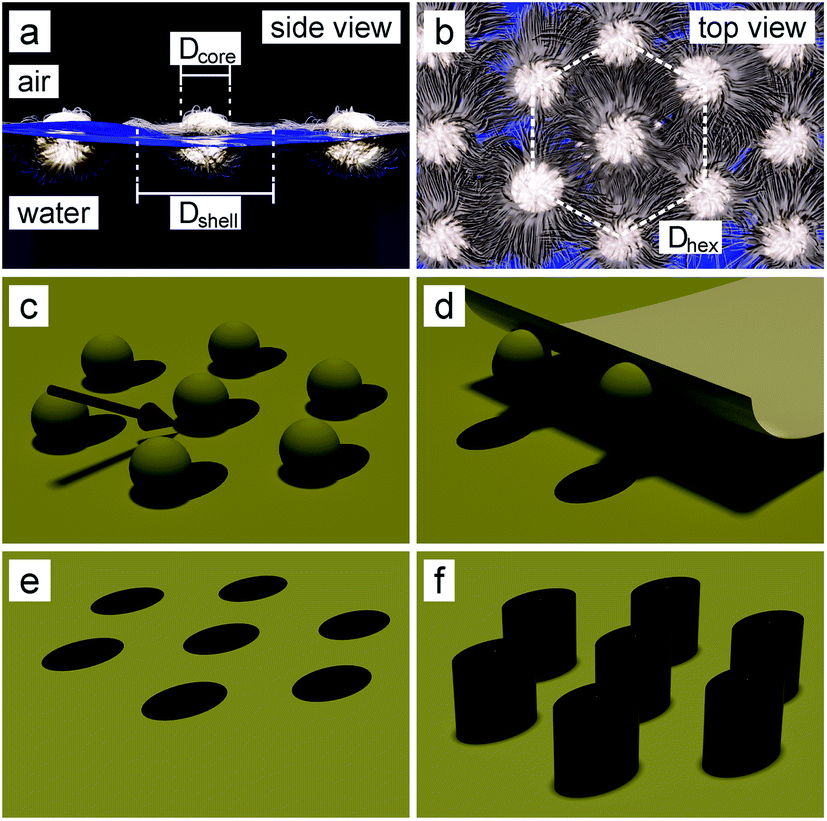 | ||
| Fig. 1 Schematic illustration of the colloidal lithography approach to obtain elliptical SiNW arrays. (a and b) SiO2–PNIPAM core–shell particles are self-assembled into a hexagonal lattice at the air/water interface. (c) After transfer of the colloidal monolayer onto a silicon substrate and removal of the polymeric shell by oxygen plasma, an Au layer is evaporated under an oblique angle, resulting in an elliptical shadow cast by the colloidal particle. (d and e) After removal of the colloidal particles by adhesive tape, the elliptical hole array mask is obtained. (f) Fabrication of SiNW arrays with an elliptical cross-section using metal-assisted chemical etching (MACE). | ||
In the next step, 20–40 nm Au with 3–5 nm Ti as adhesion layer is thermally evaporated under an oblique angle (Figure 1c and 2a–d: top). After removal of the SiO2 particles using adhesive tape (Fig. 1d), an elliptical hole mask is obtained (Figure 1e and 2a–d: bottom). We then etch elliptical SiNWs using MACE by dipping the substrates into an aqueous solution containing 10![[thin space (1/6-em)]](https://www.rsc.org/images/entities/char_2009.gif) :1:10 HF:H2O2:H2O for 3–20 minutes, depending on the desired SiNW length. Hereby the Au layer catalyses the dissolution of silicon beneath the layer,25,26 leading to the etching of ordered, vertically-aligned SiNWs (Fig. 1f and 3). The aspect ratio (AR) of the elliptical cross-section, and with this the shape of the resulting nanowire arrays (Fig. 3a and b), can be tuned by the evaporation angle up to 2.6. Additionally, low magnification SEM images and photographs of the etched substrates show the high homogeneity and reliability of the etching process (Fig. 3c and d).
:1:10 HF:H2O2:H2O for 3–20 minutes, depending on the desired SiNW length. Hereby the Au layer catalyses the dissolution of silicon beneath the layer,25,26 leading to the etching of ordered, vertically-aligned SiNWs (Fig. 1f and 3). The aspect ratio (AR) of the elliptical cross-section, and with this the shape of the resulting nanowire arrays (Fig. 3a and b), can be tuned by the evaporation angle up to 2.6. Additionally, low magnification SEM images and photographs of the etched substrates show the high homogeneity and reliability of the etching process (Fig. 3c and d).
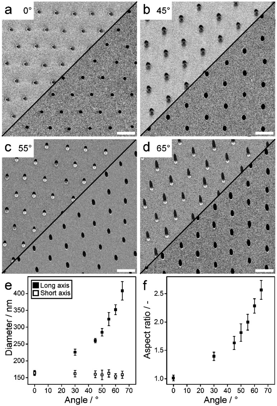 | ||
| Fig. 2 Elliptical nanohole arrays to be used as etching masks in the MACE process, formed by oblique evaporation of a Ti/Au layer onto a non-close packed colloidal monolayer. (a–d) SEM images of the metal nanohole arrays. (Top) Prior to the removal of the silica spheres and (Bottom) after removing the silica spheres using adhesive tape. Scale bars: 1 μm. (e and f) Measured short and long cross-sectional diameter and respective aspect ratio as a function of evaporation angle. | ||
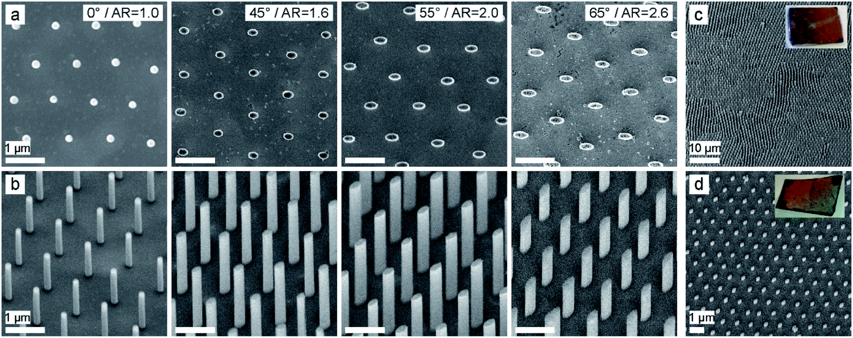 | ||
| Fig. 3 Vertically-aligned SiNW arrays with tunable, anisotropic cross-section defined by the evaporation angle of the metal film on the colloidal mask. Spherical cross-sections result from normal evaporation (0°); elliptical cross-sections with tailored aspect ratio result from oblique evaporation (45°, 55°, 65°). The aspect ratio (AR) varies from 1–2.6. (a) Top view SEM images. (b) 30° tilted SEM images. The length of the SiNW is between 2–5 μm. Scale bars: 1 μm. (c and d) Low-magnification 30° tilted SEM images and photograph of the etched Si wafer of elliptical SiNWs with an AR of 2.0, etched for 5 min (length ∼ 3 μm) (c) and for 3 min (length ∼ 0.4 μm) (d). The Au layer was removed using a KI/I2 solution. | ||
After MACE, the substrates are thoroughly washed in ethanol and left to dry. The evaporation of the solvent trapped within the array can generate strong capillary forces associated with the liquid/vapor meniscus between the tips of the SiNWs. This can cause the deformation and even collapse of the SiNWs, leading to bundling.57–59 Alternatively, supercritical CO2 drying can be used to reduce the occurrence of bundling.60 The bundling can be described by the competition between the capillary force (FC), which attracts neighboring pillars, and the elastic deformation force (FE), which resists the bending.50 The capillary force depends on the surface tension of the liquid (γ), the height (h) and the long axis of the SiNW (a), the solid–liquid contact angle (θ) and the distance between the SiNW (s) (FC ∼ γhacos(θ)s−1).49 The elastic deformation force is FE ∼ EIδxh−3, where E is the Young's modulus, I is the second moment of area and δx the deformation length.61 Bending of two neighboring wires towards each other results when FC > FE. The capillary-induced bundling behavior of pillars with various cross-sections has been previously investigated for polymeric pillar arrays obtained by laser printing49,52–54 or photolithography.50,51 The flexible nature of the polymeric pillars (E ∼ 0.1–2 GPA) allowed the pillars to not only bend but also twist into hierarchical helical assemblies.50 Here we investigate the capillary-induced bundling behavior of much stiffer SiNWs (E ∼ 130–170 GPA)62 as a function of cross-sectional shape.
For a SiNW with a rotationally symmetric circular cross-section, I = ¼πr4, where r is the cylinder radius, and thus their bending direction should be random. The equal distance between the SiNWs leads to the bundling into “flower-like” structures (Fig. 4a and b). Noteworthily, the high Young's modulus of the SiNW prevents them from twisting into hierarchical helical assemblies. On the other hand, for SiNWs with an elliptical cross-section, FE and FC depend on the bending direction. The second moment of area of the SiNW with an elliptical cross-section bending into the direction of the long axis is Ia = ¼πa3b, and in the direction of the short axis Ib = ¼πab3, where a is the long axis and b the short axis. Thus, the elastic force is smaller in the direction of the short axis and the pillars preferably bend in this direction.49 This preferential bending direction leads to anisotropic, linear hierarchical mesostructures, which are oriented along the direction of the long axis of the SiNW (Fig. 4c–f). Such oriented SiNW mesostructures may have potential application in nanobiotechnology, as they may guide the growth of cells.63,64 Furthermore, their anisotropic topography may produce anisotropic wettability and guide the flow of water droplets, comparable to the natural example of the rice leaf, which has a similar morphology.65–67
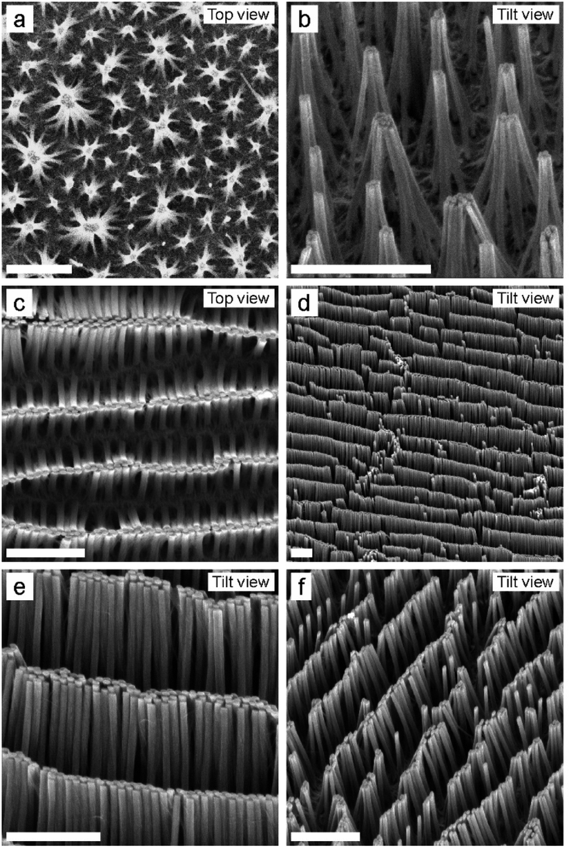 | ||
| Fig. 4 Anisotropic mesostructures created by controlling capillary-induced pillar collapse. (a and b) Nanowires with a spherical cross-section bundle with their closest neighbors to a circular, “flower-like” mesostructure. (c–f) Nanowires with an elliptical cross-section preferably bend in the direction of their minor axis as the respective bending modulus scales with the thickness of the nanowires. This leads to defined bundling into oriented, anisotropic linear mesostructures. Scale bar: 5 μm. | ||
Last, we demonstrate the fabrication of SiNWs with a crescent-shaped cross-section (Fig. 5). To this end, we follow a similar etching protocol but do not remove the SiO2 particles after angular evaporation of the Au layer. Instead, we use the patterns as shown in Fig. 2 (top images) and perform the MACE process as schematically illustrated in Fig. 5a and e. When dipped into the MACE solution, the SiO2 particles are immediately dissolved by HF, but the Au cap, which covered the sphere, remains attached to the Au layer. During the sinking of the Au layer, the Au caps come into contact with the elliptical SiNW and etch a circular hole into the elliptical SiNW. Therefore, we obtain crescent-shaped SiNWs, where the wall thickness can be adjusted by the evaporation angle (Fig. 5). While the SiNWs evaporated under a 55° angle remain stable, the thinner SiNWs evaporated under a 30° angle bend preferentially in the concave direction of the crescent. Interestingly, since the Au catalyst layer is now not completely flat but has a 3D structure (the film is increased by 160 nm at the position of the SiO2 particles), the resulting SiNW array is also not fully flat at the bottom. After removal of the Au layer by a KI/I2 solution, there is still a spherical attachment at the bottom of each SiNW, reminiscent of the elevated topography of the initial colloidal particle (Fig. 5b–d and f–h).
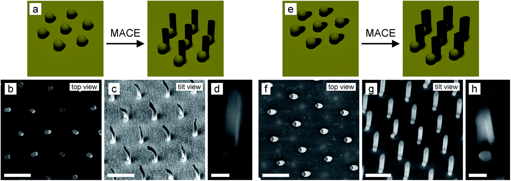 | ||
| Fig. 5 Process to obtain SiNW with a crescent-shaped cross-section with a thin wall thickness (a–d) and thick wall thickness (e–h). (a and e) Schematic illustration of the etching process to obtain crescent-shaped SiNW with different wall thicknesses. (b–d) SEM images of thin crescent-shaped SiNW evaporated under a 30° angle. (f–h) SEM images of thick crescent-shaped SiNW evaporated under a 55° angle. The Au layer was removed using KI/I2 solution. (c, d, f and h) Scale bar: 1 μm. (d and h) Scale bar: 200 nm. | ||
Conclusion
To summarize, we developed a simple and affordable technique to synthesize large-scale, homogeneous SiNW arrays with tunable anisotropic cross-sections. The approach utilizes the shadow of the templating colloidal particles under angular thermal evaporation, where the aspect-ratio of the elliptical holes can be adjusted with the evaporation angle. When the templating spheres are removed, the metal-assisted chemical etching results in SiNWs with elliptical cross-sections or, when the templating spheres remain on the surface, in nanowires with crescent shaped cross-sections. We further demonstrate the anisotropic bundling of nanowires with elliptical cross-sections upon capillary-induced collapse. The anisotropic collapse along their short axis results in anisotropic, linear mesostructures. These results demonstrate that a rich library of SiNW shapes and mesostructures is possible using simple spherical colloidal particles as masks.Funding sources
The research was supported by the Deutsche Forschungsgemeinschaft (DFG) under grant number VO 1824/6-2. M. R. acknowledges funding from the Swiss National Science Foundation Project-ID P2SKP2_194953 and temporary funding from EAM. N. V. also acknowledges support by the Interdisciplinary Center for Functional Particle Systems (FPS). G. R. B. and J. F. W. gratefully acknowledge support from the Austrian Science Fund FWF for project P-33159.Author contributions
J. J. T. synthesized the core–shell particles. R. S. B and M. R. self-assembled and deposited the particles onto a substrate. E. S. A. G. evaporated the catalyst layers. F. J. W. and M. R. etched the SiNW using MACE. M. R., F. J. W., G. B. and N. V. designed the experiments and the study. All authors contributed to the writing of the manuscript.Conflicts of interest
There are no conflicts to declare.Acknowledgements
We thank Grant Osborne for his help with the 3D-printer to prepare the sample holders used for MACE.References
- E. Garnett and P. Yang, Light trapping in silicon nanowire solar cells, Nano Lett., 2010, 10(3), 1082–1087 CrossRef CAS PubMed.
- M. D. Kelzenberg, S. W. Boettcher, J. A. Petykiewicz, D. B. Turner-Evans, M. C. Putnam and E. L. Warren, et al., Enhanced absorption and carrier collection in Si wire arrays for photovoltaic applications, Nat. Mater., 2010, 9(3), 239–244 CrossRef CAS PubMed.
- K. Seo, M. Wober, P. Steinvurzel, E. Schonbrun, Y. Dan and T. Ellenbogen, et al., Multicolored vertical silicon nanowires, Nano Lett., 2011, 11(4), 1851–1856 CrossRef CAS PubMed.
- J. Proust, F. Bedu, B. Gallas, I. Ozerov and N. Bonod, All-dielectric colored metasurfaces with silicon mie resonators, ACS Nano, 2016, 10(8), 7761–7767 CrossRef CAS PubMed.
- O. Yavas, M. Svedendahl, P. Dobosz, V. Sanz and R. Quidant, On-a-chip biosensing based on all-dielectric nanoresonators, Nano Lett., 2017, 17(7), 4421–4426 CrossRef CAS PubMed.
- J. Oh, H. C. Yuan and H. M. Branz, An 18.2%-efficient black-silicon solar cell achieved through control of carrier recombination in nanostructures, Nat. Nanotechnol., 2012, 7(11), 743–748 CrossRef CAS PubMed.
- H. Savin, P. Repo, G. Von Gastrow, P. Ortega, E. Calle and M. Garín, et al., Black silicon solar cells with interdigitated back-contacts achieve 22.1% efficiency, Nat. Nanotechnol., 2015, 10(7), 624–628 CrossRef CAS PubMed.
- W. Vijselaar, P. Westerik, J. Veerbeek, R. M. Tiggelaar, E. Berenschot and N. R. Tas, et al., Spatial decoupling of light absorption and catalytic activity of Ni-Mo-loaded high-aspect-ratio silicon microwire photocathodes, Nat. Energy, 2018, 3(3), 185–192 CrossRef CAS.
- J. Deng, Y. Su, D. Liu, P. Yang, B. Liu and C. Liu, Nanowire photoelectrochemistry, Chem. Rev., 2019, 119(15), 9221–9259 CrossRef CAS PubMed.
- J. Cambiasso, M. König, E. Cortés, S. Schlücker and S. A. Maier, Surface-enhanced spectroscopies of a molecular monolayer in an all-dielectric nanoantenna, ACS Photonics, 2018, 5(4), 1546–1557 CrossRef CAS.
- S. Aslanoglou, Y. Chen, V. Oorschot, Z. Trifunovic, E. Hanssen and K. Suu, et al., Efficient transmission electron microscopy characterization of cell-nanostructure interfacial interactions, J. Am. Chem. Soc., 2020, 142(37), 15649–15653 CrossRef CAS PubMed.
- Y. Chen, J. Wang, X. Li, N. Hu, N. H. Voelcker and X. Xie, et al., Emerging roles of 1D vertical nanostructures in orchestrating immune cell functions, Adv. Mater., 2020, 32(40), 1–25 CrossRef PubMed.
- E. Lestrell, F. Patolsky, N. H. Voelcker and R. Elnathan, Engineered nano-bio interfaces for intracellular delivery and sampling: applications, agency and artefacts, Mater. Today, 2020, 33(March), 87–104 CrossRef CAS.
- A. A. Karanastasis, Y. Zhang, G. S. Kenath, M. D. Lessard, J. Bewersdorf and C. K. Ullal, 3D mapping of nanoscale crosslink heterogeneities in microgels, Mater. Horiz., 2018, 5(6), 1130–1136 RSC.
- Y. Chen, S. Aslanoglou, G. Gervinskas, H. Abdelmaksoud, N. H. Voelcker and R. Elnathan, Cellular deformations induced by conical silicon nanowire arrays facilitate gene delivery, Small, 2019, 15(47), 1904819 CrossRef CAS PubMed.
- R. Elnathan, B. Delalat, D. Brodoceanu, H. Alhmoud, F. J. Harding and K. Buehler, et al., Maximizing transfection efficiency of vertically aligned silicon nanowire arrays, Adv. Funct. Mater., 2015, 25(46), 7215–7225 CrossRef CAS.
- R. Elnathan, L. Isa, D. Brodoceanu, A. Nelson, F. J. Harding and B. Delalat, et al., Versatile particle-based route to engineer vertically aligned silicon nanowire arrays and nanoscale pores, ACS Appl. Mater. Interfaces, 2015, 7(42), 23717–23724 CrossRef CAS PubMed.
- F. J. Wendisch, M. Abazari, H. Mahdavi, M. Rey, N. Vogel and M. Musso, et al., Morphology-graded silicon nanowire arrays via chemical etching: engineering optical properties at the nanoscale and macroscale, ACS Appl. Mater. Interfaces, 2020, 12(11), 13140–13147 CrossRef PubMed.
- M. Rey, R. Elnathan, R. Ditcovski, K. Geisel, M. Zanini and M. A. Fernandez-Rodriguez, et al., Fully tunable silicon nanowire arrays fabricated by soft nanoparticle templating, Nano Lett., 2016, 16(1), 157–163 CrossRef PubMed.
- C. Chiappini, E. De Rosa, J. O. Martinez, X. Liu, J. Steele and M. M. Stevens, et al., Biodegradable silicon nanoneedles delivering nucleic acids intracellularly induce localized in vivo neovascularization, Nat. Mater., 2015, 14(5), 532–539 CrossRef CAS PubMed.
- A. M. Morales and C. M. Lieber, A laser ablation method for the synthesis of crystalline semiconductor nanowires, Science, 1998, 279(5348), 208–211 CrossRef CAS PubMed.
- V. Schmidt, J. V. Wittemann, S. Senz and U. Gósele, Silicon nanowires: a review on aspects of their growth and their electrical properties, Adv. Mater., 2009, 21(25–26), 2681–2702 CrossRef CAS.
- B. M. Kayes, M. A. Filler, M. C. Putnam, M. D. Kelzenberg, N. S. Lewis and H. A. Atwater, Growth of vertically aligned Si wire arrays over large areas (>1 cm2) with Au and Cu catalysts, Appl. Phys. Lett., 2007, 91(10), 2005–2008 CrossRef.
- Y. J. Hung, S. L. Lee, B. J. Thibeault and L. A. Coldren, Fabrication of highly ordered silicon nanowire arrays with controllable sidewall profiles for achieving low-surface reflection, IEEE J. Sel. Top. Quantum Electron., 2011, 17(4), 869–877 CAS.
- Z. Huang, H. Fang and J. Zhu, Fabrication of silicon nanowire arrays with controlled diameter, length, and density, Adv. Mater., 2007, 19(5), 744–748 CrossRef CAS.
- Z. Huang, N. Geyer, P. Werner, J. De Boor and U. Gösele, Metal-assisted chemical etching of silicon: a review, Adv. Mater., 2011, 23(2), 285–308 CrossRef CAS PubMed.
- M. A. Johar, T. Kim, H.-G. Song, A. Waseem, J.-H. Kang and M. Afifi Hassan, et al., Three-dimensional hierarchical semi-polar GaN/InGaN MQW coaxial nanowires on a patterned Si nanowire template, Nanoscale Adv., 2020, 2(4), 1654–1665 RSC.
- A. Pevzner, Y. Engel, R. Elnathan, T. Ducobni, M. Ben-ishai and K. Reddy, et al., Knocking down highly-ordered large-scale nanowire arrays, Nano Lett., 2010, 10(4), 1202–1208 CrossRef CAS PubMed.
- K. Salaita, Y. Wang and C. A. Mirkin, Applications of dip-pen nanolithography, Nat. Nanotechnol., 2007, 2(3), 145–155 CrossRef CAS PubMed.
- V. Lotito and T. Zambelli, Approaches to self-assembly of colloidal monolayers: a guide for nanotechnologists, Adv. Colloid Interface Sci., 2017, 246, 217–274 CrossRef CAS PubMed.
- B. Ai, Y. Yu, H. Möhwald, G. Zhang and B. Yang, Plasmonic films based on colloidal lithography, Adv. Colloid Interface Sci., 2014, 206, 5–16 CrossRef CAS PubMed.
- N. Vogel, M. Retsch, C. A. Fustin, A. Del Campo and U. Jonas, Advances in colloidal assembly: the design of structure and hierarchy in two and three dimensions, Chem. Rev., 2015, 115(13), 6265–6311 CrossRef CAS PubMed.
- N. Vogel, S. Goerres, K. Landfester and C. K. Weiss, A convenient method to produce close- and non-close-packed monolayers using direct assembly at the air-water interface and subsequent plasma-induced size reduction, Macromol. Chem. Phys., 2011, 212(16), 1719–1734 CrossRef CAS.
- S. H. Lee, K. C. Bantz, N. C. Lindquist, S. H. Oh and C. L. Haynes, Self-assembled plasmonic nanohole arrays, Langmuir, 2009, 25(23), 13685–13693 CrossRef CAS PubMed.
- J. Yeom, D. Ratchford, C. R. Field, T. H. Brintlinger and P. E. Pehrsson, Decoupling diameter and pitch in silicon nanowire arrays made by metal-assisted chemical etching, Adv. Funct. Mater., 2014, 24(1), 106–116 CrossRef CAS.
- F. J. Wendisch, M. Rey, N. Vogel and G. R. Bourret, Large-scale synthesis of highly uniform silicon nanowire arrays using metal-assisted chemical etching, Chem. Mater., 2020, 32(21), 9425–9434 CrossRef CAS PubMed.
- M. Rey, T. Yu, R. Guenther, K. Bley and N. Vogel, A dirty story: improving colloidal monolayer formation by understanding the effect of impurities at the air/water interface, Langmuir, 2019, 35(1), 95–103 CrossRef CAS PubMed.
- L. Isa, K. Kumar, M. Müller, J. Grolig, M. Textor and E. Reimhult, Particle lithography from colloidal self-assembly at liquid-liquid interfaces, ACS Nano, 2010, 4(10), 5665–5670 CrossRef CAS PubMed.
- J. S. J. Tang, R. S. Bader, E. S. A. Goerlitzer, J. F. Wendisch, G. R. Bourret and M. Rey, et al., Surface patterning with SiO2@PNiPAm core–shell particles, ACS Omega, 2018, 3(9), 12089–12098 CrossRef CAS PubMed.
- M. Rey, A. D. Law, D. M. A. Buzza and N. Vogel, Anisotropic self-assembly from isotropic colloidal building blocks, J. Am. Chem. Soc., 2017, 139(48), 17464–17473 CrossRef CAS PubMed.
- M. Rey, M. A. Fernandez-Rodriguez, M. Karg, L. Isa and N. Vogel, Poly-N-isopropylacrylamide nanogels and microgels at fluid interfaces, Acc. Chem. Res., 2020, 53(2), 414–424 CrossRef CAS PubMed.
- W. R. Somerville, A. D. Law, M. Rey, N. Vogel, A. J. Archer and D. M. A. Buzza, Pattern formation in two-dimensional hard-core/soft-shell systems with variable soft shell profiles, Soft Matter, 2020, 16(14), 3564–3573 RSC.
- S. Ciarella, M. Rey, J. Harrer, N. Holstein, M. Ickler, H. Lowen, et al., Soft particles at liquid interfaces: from molecular particle architecture to collective phase behavior, 2020, arXiv Prepr arXiv, available from: http://arxiv.org/abs/2008.13695.
- M. A. Fernandez-Rodriguez, R. Elnathan, R. Ditcovski, F. Grillo, G. M. Conley and F. Timpu, et al., Tunable 2D binary colloidal alloys for soft nanotemplating, Nanoscale, 2018, 10(47), 22189–22195 RSC.
- F. J. Wendisch, R. Oberreiter, M. Salihovic, M. S. Elsaesser and G. R. Bourret, Confined etching within 2D and 3D colloidal crystals for tunable nanostructured templates: local environment matters, ACS Appl. Mater. Interfaces, 2017, 9(4), 3931–3939 CrossRef CAS PubMed.
- T. Wang, X. Li, J. Zhang, X. Wang, X. Zhang and X. Zhang, et al., Elliptical silicon arrays with anisotropic optical and wetting properties, Langmuir, 2010, 26(16), 13715–13721 CrossRef CAS PubMed.
- T. Wang, X. Li, J. Zhang, Z. Ren, X. Zhang and X. Zhang, et al., Morphology-controlled two-dimensional elliptical hemisphere arrays fabricated by a colloidal crystal based micromolding method, J. Mater. Chem., 2010, 20(1), 152–158 RSC.
- H. Park and K. B. Crozier, Elliptical silicon nanowire photodetectors for polarization-resolved imaging, Opt. Express, 2015, 23(6), 7209–7216 CrossRef CAS PubMed.
- Z. Lao, Y. Hu, C. Zhang, L. Yang, J. Li and J. Chu, et al., Capillary force driven self-assembly of anisotropic hierarchical structures prepared by femtosecond laser 3D printing and their applications in crystallizing microparticles, ACS Nano, 2015, 9(12), 12060–12069 CrossRef CAS PubMed.
- B. Pokroy, S. H. Kang, L. Mahadevan and J. Aizenberg, Self-organization of a mesoscale bristle into ordered, hierarchical helical assemblies, Science, 2009, 323(5911), 237–240 CrossRef CAS PubMed.
- S. H. Kang, B. Pokroy, L. Mahadevan and J. Aizenberg, Control of shape and size of nanopillar assembly by adhesion-mediated elastocapillary interaction, ACS Nano, 2010, 4(11), 6323–6331 CrossRef CAS PubMed.
- D. Wu, Q.-D. Chen, B.-B. Xu, J. Jiao, Y. Xu and H. Xia, et al., Self-organization of polymer nanoneedles into large-area ordered flowerlike arrays, Appl. Phys. Lett., 2009, 95(9), 91902 CrossRef.
- Y. Hu, Z. Lao, B. P. Cumming, D. Wu, J. Li and H. Liang, et al., Laser printing hierarchical structures with the aid of controlled capillary-driven self-assembly, Proc. Natl. Acad. Sci. U. S. A., 2015, 112(22), 6876–6881 CrossRef CAS PubMed.
- D. Wu, S.-Z. Wu, S. Zhao, J. Yao, J.-N. Wang and Q.-D. Chen, et al., Rapid, controllable fabrication of regular complex microarchitectures by capillary assembly of micropillars and their application in selectively trapping/releasing microparticles, Small, 2013, 9(5), 760–767 CrossRef CAS PubMed.
- A. Rauh, M. Rey, L. Barbera, M. Zanini, M. Karg and L. Isa, Compression of hard core–soft shell nanoparticles at liquid–liquid interfaces: influence of the shell thickness, Soft Matter, 2017, 13(1), 158–169 RSC.
- K. Geisel, L. Isa and W. Richtering, Unraveling the 3D localization and deformation of responsive microgels at oil/water interfaces: a step forward in understanding soft emulsion stabilizers, Langmuir, 2012, 28(45), 15770–15776 CrossRef CAS PubMed.
- A. S. Togonal, L. He and P. Roca I Cabarrocas, Effect of wettability on the agglomeration of silicon nanowire arrays fabricated by metal-assisted chemical etching, Langmuir, 2014, 30(34), 10290–10298 CrossRef CAS PubMed.
- Y.-P. Zhao and J.-G. Fan, Clusters of bundled nanorods in nanocarpet effect, Appl. Phys. Lett., 2006, 88(10), 103123 CrossRef.
- I. V. Bagal, M. A. Johar, M. A. Hassan, A. Waseem and S.-W. Ryu, Facile morphology control of high aspect ratio patterned Si nanowires by metal-assisted chemical etching, J. Mater. Sci.: Mater. Electron., 2018, 29(21), 18167–18177 CrossRef CAS.
- C. Choi, Y. Yoon, D. Hong, K. S. Brammer, K. Noh and Y. Oh, et al., Strongly superhydrophobic silicon nanowires by supercritical CO2 drying, Electron. Mater. Lett., 2010, 6(2), 59–64 CrossRef CAS.
- J. Song, X. Wang, E. Riedo and Z. L. Wang, Elastic property of vertically aligned nanowires, Nano Lett., 2005, 1–5 CAS.
- M. A. Hopcroft, W. D. Nix and T. W. Kenny, What is the Young's modulus of silicon?, J. Microelectromech. Syst., 2010, 19(2), 229–238 CAS.
- P. Clark, P. Connolly, A. S. G. Curtis, J. A. T. Dow and C. D. W. Wilkinson, Topographical control of cell behaviour: II. multiple grooved substrata, Development, 1990, 108(4), 635–644 CrossRef CAS.
- F. Johansson, P. Carlberg, N. Danielsen, L. Montelius and M. Kanje, Axonal outgrowth on nano-imprinted patterns, Biomaterials, 2006, 27(8), 1251–1258 CrossRef CAS PubMed.
- D. Wu, J. N. Wang, S. Z. Wu, Q. D. Chen, S. Zhao and H. Zhang, et al., Three-level biomimetic rice-leaf surfaces with controllable anisotropic sliding, Adv. Funct. Mater., 2011, 21(15), 2927–2932 CrossRef CAS.
- S. G. Lee, H. S. Lim, D. Y. Lee, D. Kwak and K. Cho, Tunable anisotropic wettability of rice leaf-like wavy surfaces, Adv. Funct. Mater., 2013, 23(5), 547–553 CrossRef CAS.
- J. Long, P. Fan, D. Jiang, J. Han, Y. Lin and M. Cai, et al., Anisotropic sliding of water droplets on the superhydrophobic surfaces with anisotropic groove-like micro/nano structures, Adv. Mater. Interfaces, 2016, 3(24), 1–8 CrossRef.
Footnote |
| † These authors contributed equally. |
| This journal is © The Royal Society of Chemistry 2021 |