
 Open Access Article
 This Open Access Article is licensed under a Creative Commons Attribution-Non Commercial 3.0 Unported Licence
Type-II lateral SnSe/GeTe heterostructures for solar photovoltaic applications with high efficiency†
Qianyong
Zhuang
ab,
Jin
Li
 *ab,
Chaoyu
He
ab,
Tao
Ouyang
ab,
Chunxiao
Zhang
ab,
Chao
Tang
*ab and
Jianxin
Zhong
ab
*ab,
Chaoyu
He
ab,
Tao
Ouyang
ab,
Chunxiao
Zhang
ab,
Chao
Tang
*ab and
Jianxin
Zhong
ab
aHunan Key Laboratory of Micro-Nano Energy Materials and Devices, Xiangtan University, Hunan 411105, People's Republic of China. E-mail: lijin@xtu.edu.cn; tang_chao@xtu.edu.cn
bSchool of Physics and Optoelectronics, Xiangtan University, Hunan 411105, People's Republic of China
First published on 7th May 2021
Abstract
Recently, lateral heterostructures based on two-dimensional (2D) materials have provided new opportunities for the development of photovoltaic nanodevices. In this work, we propose a novel lateral SnSe/GeTe heterostructure (LHS) with high photovoltaic performance and systematically investigate the structural, electronic and optical properties of the lateral heterostructure by using first-principles calculations. Our results show that this type of heterostructure processes excellent stability due to the small lattice mismatch and formation energy and also covalent bonding at the interface, which is greatly beneficial for the epitaxial growth of heterostructures. These heterostructures are semiconductors with type-II band alignment and their electronic properties can be effectively tuned by the size and composition ratio of the heterostructures. More importantly, it is found that these heterostructures possess high absorption over a wide range of visible light and high power conversion efficiency (up to 22.3%). These extraordinary properties make the SnSe/GeTe lateral heterostructures ideal candidates for photovoltaic applications.
1. Introduction
As an environmentally friendly energy utilization program, solar photovoltaic power generation has made a great contribution to solving the world's energy shortage problem.1 Currently, the main obstacle to the use of solar energy is the lack of photovoltaic materials with high conversion efficiency from sunlight to electricity.2 Due to the ultra-high specific surface area, tunable bandgap and high light absorption rate compared to two-dimensional (2D) materials,3–5 a variety of two-dimensional semiconductor solar photovoltaic materials have been proposed lately, such as C3N4,6 2D perovskites7 and MoS2.8 However, there are often some shortcomings for single materials in applications, such as a fixed bandgap and the inability to separate electrons and holes.9 Building heterostructures from 2D materials is an effective method to modulate the properties of materials and improve device performance.10 There are two categories of two-dimensional heterostructures, i.e. vertical11–13 and lateral heterostructures.14–17 Compared to the vertical heterostructures, the lateral heterostructures have attracted enormous attention in experiments and theories due to their simpler band alignments, more distinct phase separation and covalent bonding interfaces,9,18 and also process many exotic properties compared to single materials. For example, Liu et al. obtained a graphene/h-BN LHS by making monolayer hexagonal boron grow from fresh edges of monolayer graphene, which can be used in electronic and optical spin electronic devices.19 Kang et al. showed that type-II band alignment can be established in in-plane TMD heterostructures due to the coherent lattice and strong electronic coupling and are useful for photovoltaics.20 High PCE can be achieved in in-plane heterostructures by applying external strain21 or increasing the number of layers of the 2D LHSs.22 However, intrinsic monolayer 2D heterostructures with high photovoltaic efficiency are still rare and thus it is of crucial importance to explore such 2D heterostructures.Recently, layered group-IV monochalcogenides with a similar structure to black phosphorus have attracted widespread attention for potential applications in solar energy conversion and optoelectronics,23–25 due to their suitable bandgaps (0.5–1.5 eV), high chemical and electrochemical stability in acidic or alkaline environments and abundance on Earth.26 At present, group-IV monochalcogenide films and their heterostructures are being studied by experiments and theoretical calculations. King et al. produced stable and impurity-free GeTe films through a cap-free deposition process.27 Velea et al.28 and Devasia et al.29 have reported the thermal stability and inter-diffusion effect of bilayer SnSe/GeTe as a phase change film, respectively. Sutter's group have grown a GeS/SnS lateral heterostructure using a two-step growth process, and revealed its optoelectronic applications.30 SnSe thin films have been successfully synthesized by vapor transport deposition,31 liquid phase exfoliation and solution deposition, and found that the SnSe thin films process strong optical nonlinearity32 and about 9.4% maximum photovoltaic efficiency.33 SnTe/GeS,34 GeS/SnS,35 GeS/GeSe and SnS/GeSe36 lateral heterostructures all have been studied by using first-principles calculations, and some of them have type-II band alignment and are promising for high-efficiency solar cells. These theoretical and experimental studies suggest that layered group-IV monochalcogenides could be basic materials for practical high performance photovoltaic devices.
Inspired by the development and potential applications of 2D LHSs and layered group-IV monochalcogenides, we propose a new lateral heterostructure composed of SnSe and GeTe with high stability and high power conversion efficiency. Based on first-principles calculations, it is found that the lattice mismatch and formation energy are very small and the two components are connected by covalent bonding at the interface, which endows the heterostructures with excellent stability and is greatly beneficial for the epitaxial growth of heterostructures. These heterostructures are semiconductors with type-II band alignment and their electronic properties can be effectively tuned by the size and composition ratio of the heterostructures. By investigating the optical properties, it is found that these heterostructures possess high absorption over a wide range of visible light and high power conversion efficiency (up to 22.3%). Our results indicate that SnSe/GeTe lateral heterostructures are a class of ideal materials for photovoltaic device applications.
2. Computational methods
All first-principles calculations are carried out by using the Vienna ab initio simulation package (VASP)37 with the projector-augmented-wave (PAW) approach38 and the Perdew–Burke–Ernzerhof (PBE) functional within the generalized gradient approximation (GGA).39 The cutoff energy for the plane-wave basis functions is chosen as 500 eV. To prevent the interaction between adjacent layers, a vacuum layer of 20 Å was added in the direction perpendicular to the two-dimensional heterostructure plane. In geometry optimization, all atoms are fully relaxed until the force on them is less than 0.01 eV Å−1. The Brillouin zone is sampled by using Monkhorst–Pack special k-point grids40 with sizes of 3 × 5 × 1 (armchair direction) and 5 × 3 × 1 (zigzag direction), respectively. Because the PBE method always underestimates the bandgaps, we also employ the Heyd–Scuseria–Ernzerhof (HSE06) hybrid functional41 to calculate the electronic and optical properties.3. Results and discussion
Firstly, we have determined the atomic structure and electronic properties of monolayer SnSe and GeTe, which are the basic components of the heterostructure. Our results show that the optimized lattice parameters of SnSe (GeTe) are a = 4.29 (4.24) Å and b = 4.39 (4.37) Å. According to the band structures (shown in Fig. S1†), monolayer SnSe and GeTe are indirect bandgap semiconductors and the bandgaps calculated by PBE (HSE) are 0.93 eV (1.41 eV) and 0.87 eV (1.17 eV), respectively. The total density of states and the partial density of states of the monolayer SnSe and GeTe are also shown in Fig. S1,† and it can be seen that the conduction-band minimum (CBM) is mainly contributed by the p states of Sn and Ge, while the valence-band maximum (VBM) is dominated by the p states of Se and Te. These results are in good agreement with previous calculations as listed in Table S1.†26,42 According to the structural properties of monolayer SnSe and GeTe, it is found that the lattice mismatch between SnSe and GeTe along the armchair direction (a-direction) and the zigzag direction (b-direction) is 0.4% and 1.2%, respectively. Such small lattice mismatches will benefit the formation of heterostructures along both armchair and zigzag directions with small structural deformation and strain. To describe the LHSs, according to different 1D interfaces, we use A-(SnSe)m/(GeTe)n and Z-(SnSe)m/(GeTe)n to denote the armchair and zigzag heterostructures with m building blocks of SnSe and n building blocks of GeTe, as shown in Fig. 1a and b.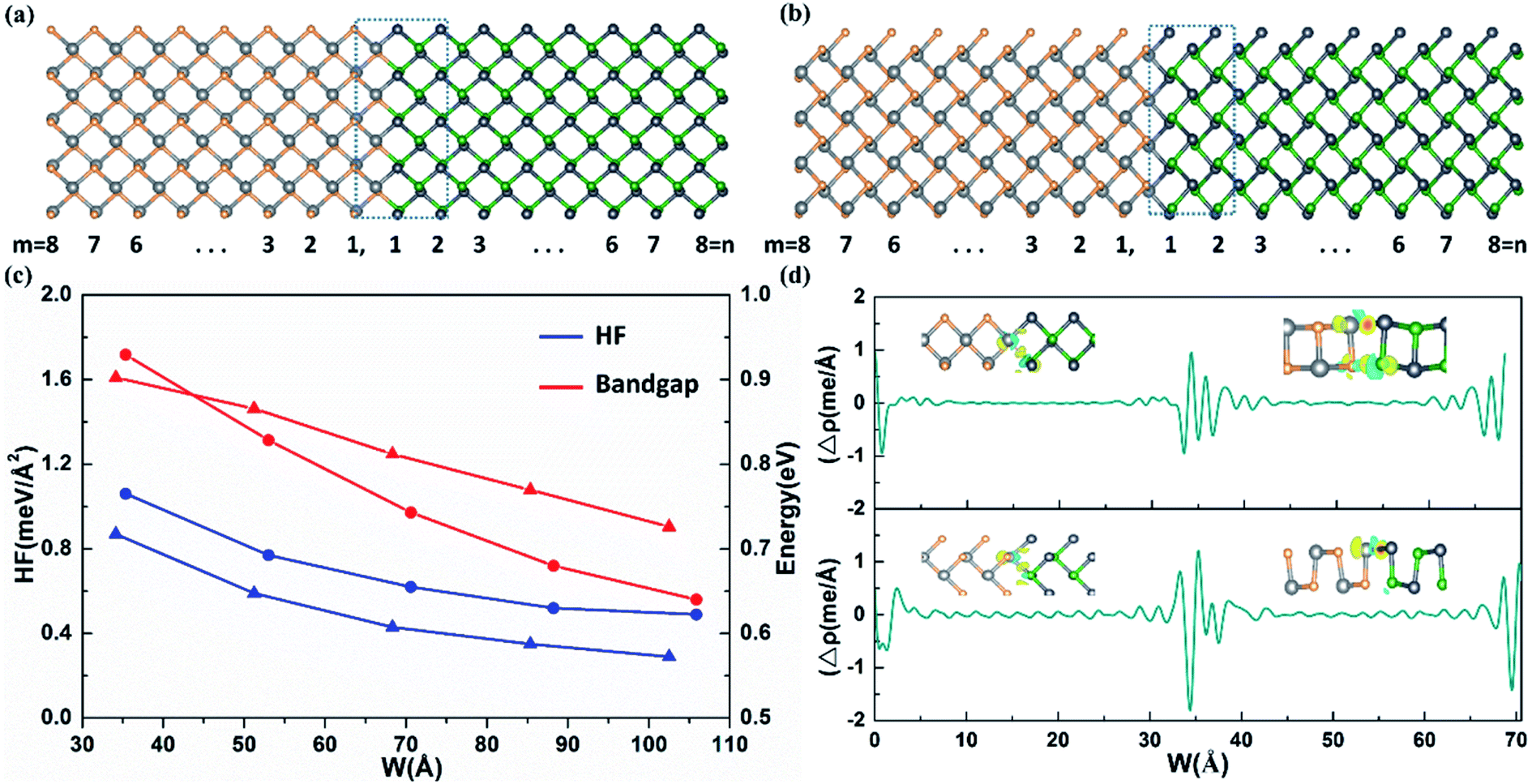 | ||
| Fig. 1 Atomic configurations of (a) A-(SnSe)8/(GeTe)8 and (b) Z-(SnSe)8/(GeTe)8 heterostructures. (c) Heats of formation (HF) and PBE bandgap values as functions of width (W); the triangle and circle represent the armchair and zigzag direction, respectively. (d) Plane-averaged electron density difference of A-(SnSe)8/(GeTe)8 (upper) and Z-(SnSe)8/(GeTe)8 (lower). The inset is a three-dimensional isosurface of the electron density difference, where the yellow and cyan regions represent electron accumulation and depletion, respectively. | ||
The thermodynamic stability of these heterostructures is estimated from the heats of formation (HF), which is defined as the energy cost of each area of the supercell:35
| HF = (EH − ESnSe − EGeTe)/(W × LH) | (1) |
In order to understand the interfacial characteristics of the heterostructure, we investigate the bonds at the interface. The lengths of Sn–Te and Ge–Se bonds at the interface of A-(SnSe)8/(GeTe)8 are 3.10 Å and 2.69 Å, and the Sn–Te bond length at the interface of Z-(SnSe)8/(GeTe)8 is 3.06 Å, which are very close to that of pure SnTe (3.14 Å) and GeTe (2.60 Å) systems.26 The result suggests that the two components in the heterostructure are connected by covalent bonds at the interface. To further confirm this and visualize the charge transfer and redistribution around the interface, the isosurface of the electron density difference and the plane-averaged electron density difference around the interface are calculated using Δρ = ρLHS − ρSnSe − ρGeTe, where ρLHS is the plane-averaged density of the lateral heterostructure, and ρSnSe and ρGeTe are the individual plane-averaged densities of the SnSe and GeTe of the lateral heterostructure. The accumulation and depletion of electrons are vividly shown in Fig. 1d, where we can clearly see that the two domains in the heterostructure are connected by covalent bonds with the accumulation of electrons between Sn–Te and Ge–Se at the interface for both armchair and zigzag type heterostructures, which is the same as that of the heterostructures with m ≠ n (shown in Fig. S3†). Due to the Coulomb shielding effect, the redistribution of electrons only occurs in the narrow area around the stitch interface.45 The covalent bonding at the interface together with the very small lattice mismatch and formation energy indicates the excellent stability of the heterostructures, which is greatly beneficial for the epitaxial growth of heterostructures.
Previous theoretical studies have revealed that the size and composition ratio may play important roles in the electronic properties of 2D LHSs.46 To investigate these effects, we firstly have studied the size effects on the bandgap of heterostructures with m(n) = 4–12 and the PBE bandgaps are shown in Fig. 1c. It is found that the bandgaps generally show a decreasing trend as the width increases, which is similar to phenomena that have occurred in other lateral heterostructures.47,48 The bandgaps of heterostructures with m(n) = 4–8 are also calculated by HSE as shown in Fig. S4† and shows the same characteristic as the PBE results. The main reason is that the quantum confinement effect and the Coulomb effect from the interface dipole weaken gradually as the LHS width increases, and the bandgap of the lateral heterostructure will converge to a fixed value.36
To investigate the effect of the component ratio on the bandgap of heterojunctions, we have calculated the band structures of armchair and zigzag (SnSe)m/(GeTe)n heterostructures with m + n = 16. The results show that all lateral heterojunctions are indirect semiconductors in Fig. 2, which is similar to that of SnSe and GeTe monolayers. For A-(SnSe)m/(GeTe)n, the CBM is located along the X–S direction and the VBM is located along the Y–G direction as m is small, while the CBM is located along the G–X direction and the VBM is still located along the Y–G direction as m is large. For Z-(SnSe)m/(GeTe)n, the CBM is located along S–Y and G–X directions for small and large m respectively, and the VBM is located along the Y–G direction for all heterostructures. Fig. 2d and h show the variations of the band gap with m from PBE and HSE methods. By comparing the results, we find that the dispersion relationships obtained by the two methods are almost the same, but the bandgap obtained by the HSE method is about 0.3 eV larger than that of the PBE method. For A-(SnSe)m/(GeTe)n, the HSE bandgap gradually increases from 1.17 eV to 1.37 eV as m increases, and the bandgap of Z-(SnSe)m/(GeTe)n varies in the range of 0.96–1.32 eV. The results indicate that the bandgap of the superlattice can be effectively tuned by the proportion of the components.
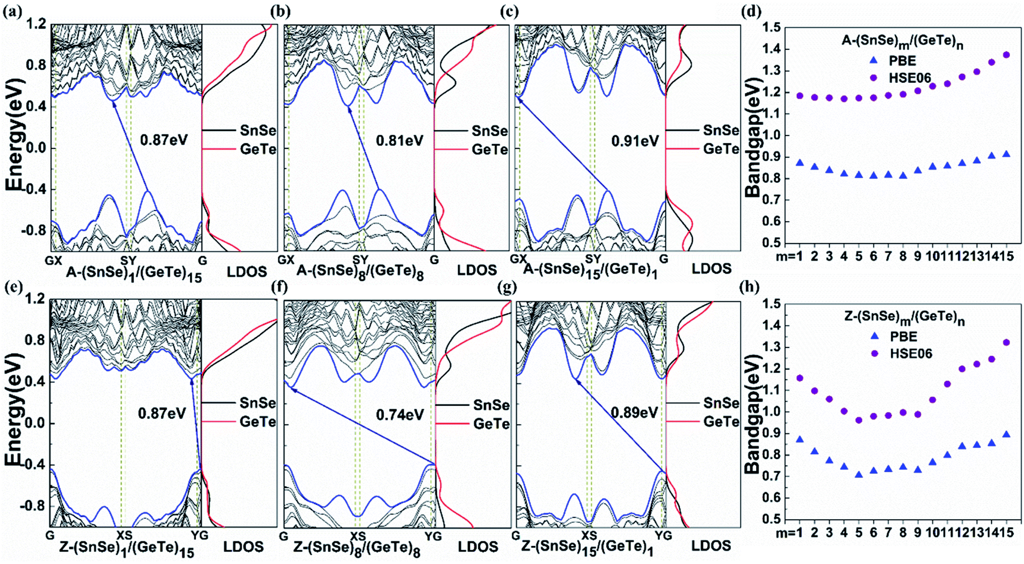 | ||
| Fig. 2 Band structures and local density of states of A-(SnSe)/(GeTe) and Z-SnSe/GeTe with different m and n are shown in (a)–(c) and (e)–(g), respectively. (d) and (h) show the m-dependent bandgaps of A-(SnSe)/(GeTe) and Z-SnSe/GeTe obtained by PBE and HSE06 methods. | ||
The band alignment of LHSs is well known to be particularly important for their applications. Because of the interface dipole potential in the attenuation of the asymptotic limit of large distances, the influence of interface conditions on band alignment can be ignored when the width of the 2D lateral junction is large enough and the band alignment can be obtained directly from the Anderson limit. However, when the width of the 2D heterostructure is small, the band alignment is mainly determined by the interface conditions and the size of the composition domain.49 Thus we calculated the band alignments according to the local density of states (LDOS) as shown in Fig. 2 and S5.† The conduction band offset (CBO) ΔEC and valence band offset (VBO) ΔEV are obtained as follows:47
| ΔEC = ERC − ELC | (2) |
| ΔEV = ERV − ELV | (3) |
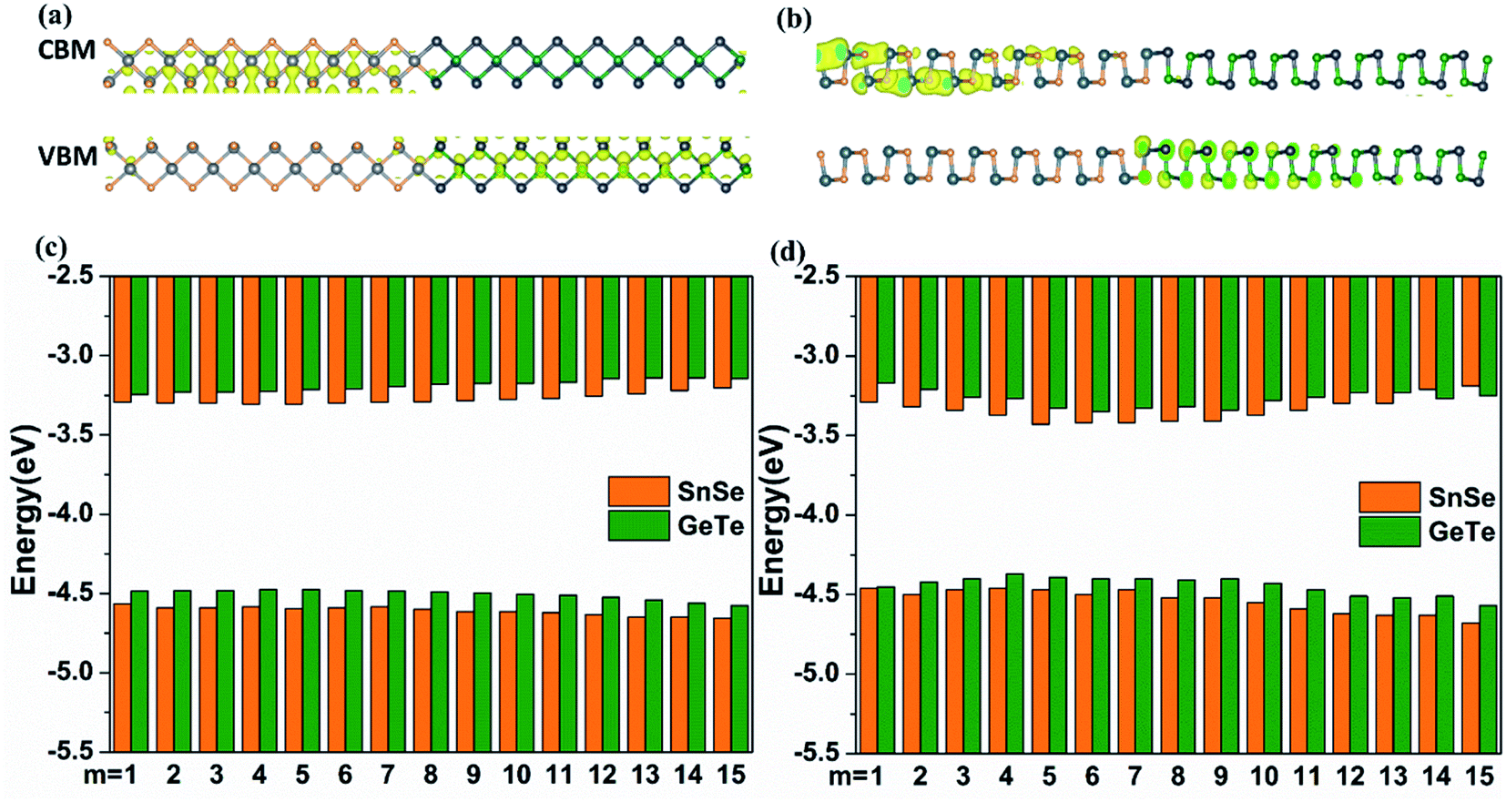 | ||
| Fig. 3 The partial charge distribution corresponding to the VBM and CBM of (a) A-(SnSe)8/(GeTe)8 and (b) Z-(SnSe)8/(GeTe)8. Band alignments of (c) A-(SnSe)m/(GeTe)n and (d) Z-(SnSe)m/(GeTe)n obtained by HSE. | ||
The bandgaps of the (SnSe)m/(GeTe)n heterostructures are about 1.0–1.4 eV, indicating that SnSe/GeTe heterostructures are suitable for solar applications.50,51 Therefore, we further estimate the optical performance of the LHSs. Firstly, the HSE optical absorption coefficient α(ω) based on the frequency-dependent dielectric function is calculated by using  . The results are shown in Fig. 4a and b. Obviously, both the armchair and zigzag LHSs have excellent absorption capacity over the range of visible light (1.6–3.2 eV) reaching 105 cm−1 orders of magnitude, which provides strong support for becoming the candidate materials for solar cells. To further characterize the optical performance of the LHS, we have also calculated its optical absorbance A(E) by using the equation A(E) = 1 − e−αΔz,51 where α is the optical absorption coefficient obtained above and Δz is the size of the supercell in the layer-normal direction. The calculated optical absorbance spectra of A-(SnSe)/(GeTe) are shown in Fig. 4c and those of Z-(SnSe)/(GeTe) are shown in Fig. 4d. Due to the in-plane anisotropy of the materials, the absorption spectra of light polarized in the zigzag or armchair direction are different. Furthermore, the absorbances of LHSs with different composition ratios are very high and the highest values are in the range of 20–33%. Then the flux of absorbed photons Jabs is calculated to quantify the above characteristics:
 | (4) |
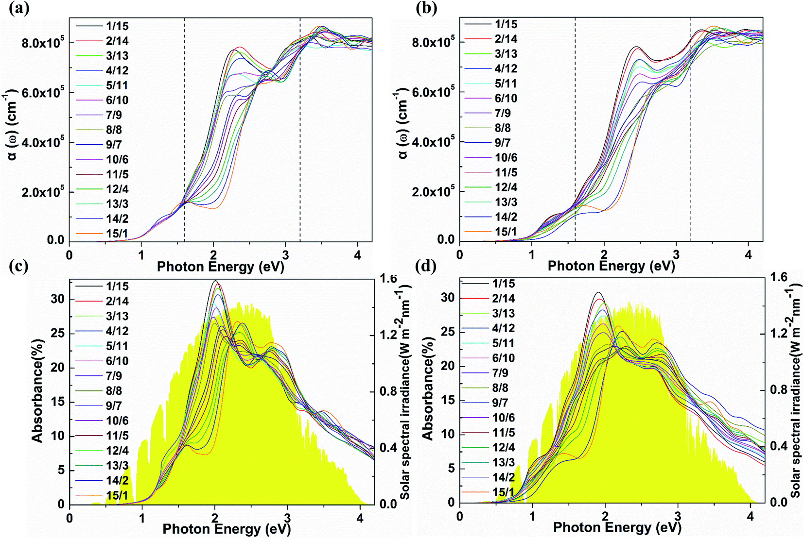 | ||
| Fig. 4 The calculated optical absorption coefficients and optical absorbance spectra of A-(SnSe)m/(GeTe)n and Z-(SnSe)m/(GeTe)n are shown in (a) and (c) and (b) and (d), respectively. The two dashed lines indicate the region of visible light and the reference air-mass 1.5-solar spectral irradiance is plotted in yellow. | ||
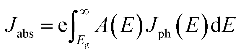
Finally, we further estimated the power conversion efficiency (PCE) following Scharber's method54 based on HSE calculations. The upper limit of PCE at the 100% external quantum efficiency limit can be expressed as:
 | (5) |
4. Conclusion
In summary, the structural, electronic and optical properties of SnSe/GeTe LHSs have been investigated systematically using first-principles calculations. The results show that the lattice mismatch and the formation energy are very small and the two compounds are covalently bonded at the interface, which indicate the excellent stability of the heterostructures. These heterostructures are semiconductors with type-II band alignment and their electronic properties can be effectively tuned by the size and composition ratio of the heterostructures. By investigating the optical properties, it is found that these heterostructures possess high absorption over a wide range of visible light and high power conversion efficiency. Our results suggest that the SnSe/GeTe heterostructures are potential candidates for high-efficiency solar photovoltaic applications, and we hope that our theoretical predictions can promote the experimental synthesis of SnSe/GeTe lateral heterostructures for optoelectronic applications.Conflicts of interest
There are no conflicts of interest to declare.Acknowledgements
This work is supported by the National Natural Science Foundation of China (11974300, 11974299, 11704319 and 11874316), the Natural Science Foundation of Hunan Province, China (2016JJ3118 and 2019JJ50577), the Program for Changjiang Scholars and the Innovative Research Team in University (IRT13093), and the Scientific Research Foundation of Education Bureau of Hunan Province (20B582, 20K127, and 20A503).References
- G. H. Carey, A. L. Abdelhady, Z. Ning, S. M. Thon, O. M. Bakr and E. H. Sargent, Chem. Rev., 2015, 115, 12732–12763 CrossRef CAS PubMed.
- H. Yang, Y. Ma, Y. Liang, B. Huang and Y. Dai, ACS Appl. Mater. Interfaces, 2019, 11, 37901–37907 CrossRef CAS PubMed.
- Q. H. Wang, K. Kalantar-Zadeh, A. Kis, J. N. Coleman and M. S. Strano, Nat. Nanotechnol., 2012, 7, 699–712 CrossRef CAS PubMed.
- K. S. Novoselov, A. K. Geim, S. V. Morozov, D. Jiang, Y. Zhang, S. V. Dubonos, I. V. Grigorieva and A. A. Firsov, Science, 2004, 306, 666–669 CrossRef CAS PubMed.
- K. S. Novoselov, D. Jiang, F. Schedin, T. Booth, V. Khotkevich, S. Morozov and A. K. Geim, Proc. Natl. Acad. Sci. U. S. A., 2005, 102, 10451–10453 CrossRef CAS PubMed.
- W.-J. Ong, L.-L. Tan, Y. H. Ng, S.-T. Yong and S.-P. Chai, Chem. Rev., 2016, 116, 7159–7329 CrossRef CAS PubMed.
- S. Chen and G. Shi, Adv. Mater., 2017, 29, 1605448 CrossRef PubMed.
- M.-L. Tsai, S.-H. Su, J.-K. Chang, D.-S. Tsai, C.-H. Chen, C.-I. Wu, L.-J. Li, L.-J. Chen and J.-H. He, ACS Nano, 2014, 8, 8317–8322 CrossRef CAS PubMed.
- J. Zhao, K. Cheng, N. Han and J. Zhang, Wiley Interdiscip. Rev.: Comput. Mol. Sci., 2018, 8, e1353 Search PubMed.
- Z. Cai, B. Liu, X. Zou and H.-M. Cheng, Chem. Rev., 2018, 118, 6091–6133 CrossRef CAS PubMed.
- A. K. Geim and I. V. Grigorieva, Nature, 2013, 499, 419–425 CrossRef CAS PubMed.
- L. Britnell, R. Ribeiro, A. Eckmann, R. Jalil, B. Belle, A. Mishchenko, Y.-J. Kim, R. Gorbachev, T. Georgiou and S. Morozov, Science, 2013, 340, 1311–1314 CrossRef CAS PubMed.
- K. S. Novoselov, A. Mishchenko, A. Carvalho and A. H. C. Neto, Science, 2016, 353, aac9439 CrossRef CAS PubMed.
- R. Martinez-Gordillo and M. Pruneda, Prog. Surf. Sci., 2015, 90, 444–463 CrossRef CAS.
- S. Haigh, A. Gholinia, R. Jalil, S. Romani, L. Britnell, D. Elias, K. Novoselov, L. Ponomarenko, A. Geim and R. Gorbachev, Nat. Mater., 2012, 11, 764–767 CrossRef CAS PubMed.
- X. Duan, C. Wang, J. C. Shaw, R. Cheng, Y. Chen, H. Li, X. Wu, Y. Tang, Q. Zhang and A. Pan, Nat. Nanotechnol., 2014, 9, 1024–1030 CrossRef CAS PubMed.
- C. Huang, S. Wu, A. M. Sanchez, J. J. Peters, R. Beanland, J. S. Ross, P. Rivera, W. Yao, D. H. Cobden and X. Xu, Nat. Mater., 2014, 13, 1096–1101 CrossRef CAS PubMed.
- M.-Y. Li, Y. Shi, C.-C. Cheng, L.-S. Lu, Y.-C. Lin, H.-L. Tang, M.-L. Tsai, C.-W. Chu, K.-H. Wei and J.-H. He, Science, 2015, 349, 524–528 CrossRef CAS PubMed.
- L. Liu, J. Park, D. A. Siegel, K. F. McCarty, K. W. Clark, W. Deng, L. Basile, J. C. Idrobo, A.-P. Li and G. Gu, Science, 2014, 343, 163–167 CrossRef CAS PubMed.
- J. Kang, H. Sahin and F. M. Peeters, J. Phys. Chem. C, 2015, 119, 9580–9586 CrossRef CAS.
- J. Lee, J. Huang, B. G. Sumpter and M. Yoon, 2D Mater., 2017, 4, 021016 CrossRef.
- K. Cheng, Y. Guo, N. Han, X. Jiang, J. Zhang, R. Ahuja, Y. Su and J. Zhao, Appl. Phys. Lett., 2018, 112, 143902 CrossRef.
- G. Xiao, Y. Wang, J. Ning, Y. Wei, B. Liu, W. Y. William, G. Zou and B. Zou, RSC Adv., 2013, 3, 8104–8130 RSC.
- L. Xu, M. Yang, S. J. Wang and Y. P. Feng, Phys. Rev. B, 2017, 95, 235434 CrossRef.
- B. U. Haq, S. AlFaify, R. Ahmed, F. K. Butt, A. Laref and M. Shkir, Phys. Rev. B, 2018, 97, 075438 CrossRef.
- L. Huang, F. Wu and J. Li, J. Chem. Phys., 2016, 144, 114708 CrossRef PubMed.
- M. R. King, B. P. Wagner, E. B. Jones, N. El-Hinnawy, P. Borodulin, S. R. McLaughlin, J. S. Mason Jr, R. S. Howell, M. J. Lee and R. M. Young, J. Vac. Sci. Technol., B: Nanotechnol. Microelectron.: Mater., Process., Meas., Phenom., 2014, 32, 041204 Search PubMed.
- A. Velea, F. Sava, G. Socol, A. Vlaicu, C. Mihai, A. Lőrinczi and I. Simandan, J. Non-Cryst. Solids, 2018, 492, 11–17 CrossRef CAS.
- A. Devasia, D. MacMahon, S. Raoux, K. A. Campbell and S. K. Kurinec, Thin Solid Films, 2012, 520, 3931–3935 CrossRef CAS.
- E. Sutter, J. Wang and P. Sutter, ACS Nano, 2020, 14, 12248–12255 CrossRef CAS PubMed.
- S. Zhao, H. Wang, Y. Zhou, L. Liao, Y. Jiang, X. Yang, G. Chen, M. Lin, Y. Wang and H. Peng, Nano Res., 2015, 8, 288–295 CrossRef CAS.
- Y. Ye, Y. Xian, J. Cai, K. Lu, Z. Liu, T. Shi, J. Du, Y. Leng, R. Wei and W. Wang, Adv. Opt. Mater., 2019, 7, 1800579 CrossRef.
- F. Liu, J. Zhu, Y. Xu, L. Zhou, Y. Li, L. Hu, J. Yao and S. Dai, Chem. Commun., 2015, 51, 8108–8111 RSC.
- H. Guo, W. Jiang, H. Fan, X. He, Y. Li and X. Tian, Phys. B, 2020, 583, 412047 CrossRef CAS.
- L. Peng, C. Wang, Q. Qian, C. Bi, S. Wang and Y. Huang, ACS Appl. Mater. Interfaces, 2017, 9, 40969–40977 CrossRef CAS PubMed.
- K. Cheng, Y. Guo, N. Han, Y. Su, J. Zhang and J. Zhao, J. Mater. Chem. C, 2017, 5, 3788–3795 RSC.
- G. Kresse and D. Joubert, Phys. Rev. B: Condens. Matter Mater. Phys., 1999, 59, 1758 CrossRef CAS.
- G. Kresse and J. Furthmüller, Phys. Rev. B: Condens. Matter Mater. Phys., 1996, 54, 11169 CrossRef CAS PubMed.
- J. P. Perdew, K. Burke and M. Ernzerhof, Phys. Rev. Lett., 1996, 77, 3865 CrossRef CAS PubMed.
- H. J. Monkhorst and J. D. Pack, Phys. Rev. B: Solid State, 1976, 13, 5188 CrossRef.
- A. V. Krukau, O. A. Vydrov, A. F. Izmaylov and G. E. Scuseria, J. Chem. Phys., 2006, 125, 224106 CrossRef PubMed.
- Z. Li, J. Li, C. He, T. Ouyang, C. Zhang, S. Zhang, C. Tang, R. A. Römer and J. Zhong, Phys. Rev. Appl., 2020, 13, 014042 CrossRef CAS.
- S. Najmaei, Z. Liu, W. Zhou, X. Zou, G. Shi, S. Lei, B. I. Yakobson, J.-C. Idrobo, P. M. Ajayan and J. Lou, Nat. Mater., 2013, 12, 754–759 CrossRef CAS PubMed.
- C. Tan and H. Zhang, J. Am. Chem. Soc., 2015, 137, 12162–12174 CrossRef CAS PubMed.
- D. Wang, D. Han, X.-B. Li, S.-Y. Xie, N.-K. Chen, W. Q. Tian, D. West, H.-B. Sun and S. Zhang, Phys. Rev. Lett., 2015, 114, 196801 CrossRef PubMed.
- O. Leenaerts, S. Vercauteren, B. Schoeters and B. Partoens, 2D Mater., 2016, 3, 025012 CrossRef.
- H.-F. Lin, L.-M. Liu and J. Zhao, J. Mater. Chem. C, 2017, 5, 2291–2300 RSC.
- Q. Sun, Y. Dai, Y. Ma, N. Yin, W. Wei, L. Yu and B. Huang, 2D Mater., 2016, 3, 035017 CrossRef.
- J. Zhang, W. Xie, J. Zhao and S. Zhang, 2D Mater., 2016, 4, 015038 CrossRef.
- Y. Liang, Y. Dai, Y. Ma, L. Ju, W. Wei and B. Huang, J. Mater. Chem. A, 2018, 6, 2073–2080 RSC.
- B. Huang, H.-X. Deng, H. Lee, M. Yoon, B. G. Sumpter, F. Liu, S. C. Smith and S.-H. Wei, Phys. Rev. X, 2014, 4, 021029 CAS.
- H. Chen, P. Yan, J. Li, C. He, T. Ouyang, C. Zhang, C. Tang and J. Zhong, J. Appl. Phys., 2020, 127, 084301 CrossRef CAS.
- M. Bernardi, M. Palummo and J. C. Grossman, Nano Lett., 2013, 13, 3664–3670 CrossRef CAS PubMed.
- M. C. Scharber, D. Mühlbacher, M. Koppe, P. Denk, C. Waldauf, A. J. Heeger and C. J. Brabec, Adv. Mater., 2006, 18, 789–794 CrossRef CAS.
- J. Zhao, Y. Li, G. Yang, K. Jiang, H. Lin, H. Ade, W. Ma and H. Yan, Nat. Energy, 2016, 1, 1–7 Search PubMed.
- M. A. Green, K. Emery, Y. Hishikawa, W. Warta and E. D. Dunlop, Prog. Photovoltaics Res. Appl., 2015, 23, 1–9 CrossRef.
- K. Wu, H. Ma, Y. Gao, W. Hu and J. Yang, J. Mater. Chem. A, 2019, 7, 7430–7436 RSC.
- M. A. Green and A. Ho-Baillie, ACS Energy Lett., 2017, 2, 822–830 CrossRef CAS.
Footnote |
| † Electronic supplementary information (ESI) available. See DOI: 10.1039/d1na00209k |
| This journal is © The Royal Society of Chemistry 2021 |