
 Open Access Article
 This Open Access Article is licensed under a Creative Commons Attribution-Non Commercial 3.0 Unported Licence
A wide-angle and TE/TM polarization-insensitive terahertz metamaterial near-perfect absorber based on a multi-layer plasmonic structure
Yuanbo
Sun
 a,
Yanpeng
Shi
*a,
Xiaoyu
Liu
a,
Jinmei
Song
a,
Meiping
Li
a,
Xiaodong
Wang
b and
Fuhua
Yang
b
a,
Yanpeng
Shi
*a,
Xiaoyu
Liu
a,
Jinmei
Song
a,
Meiping
Li
a,
Xiaodong
Wang
b and
Fuhua
Yang
b
aSchool of Microelectronics, Shandong University, Jinan 250100, China. E-mail: ypshi@sdu.edu.cn
bEngineering Research Center for Semiconductor Integrated Technology, Institute of Semiconductors, Chinese Academy of Sciences, Beijing 100083, China
First published on 2nd June 2021
Abstract
A kind of near-perfect metamaterial absorber, made of only Au and Si, has been presented in the terahertz band with extremely high absorptance. A flexible design method is proposed, which could create absorbers with four independent functions as follows. First, selective perfect absorption is achieved at a single frequency, which means the absorptance is more than 99.9% at the required frequency and almost 0% at adjacent frequencies. Second, nearly 100% perfect absorption is realized at more frequencies, which can be changed by simply adjusting the geometric parameters. Third, broadband absorption with a controllable band is gained, and the average absorptance exceeds 99% from 1.2 to 2 THz. Finally, the combination of single-frequency absorption and broadband absorption is accomplished, which greatly expands the application prospects of the proposed absorber. Besides, the absorber exhibits high performance over a wide range of incident angles from 0° to 60°. Meanwhile, it is insensitive to both TE and TM waves. The aforementioned design idea can be extended to other bands.
Introduction
Metamaterials, artificial composite materials composed of periodic subwavelength metal and dielectric resonators, have many unique electromagnetic properties that are not available in conventional materials, such as negative conductivity and permeability,1–3 negative index of refraction,4–6 invisibility cloaking,7–9etc. Due to the unique physical properties, metamaterials are widely applied in imaging,10 sensing,11,12 communication13 and detection,14 and a large number of associated devices have been produced, such as filters,15 modulators16 and detectors.17 However, in the terahertz band, because of the weak response of natural materials to terahertz signals, these devices fail to capture the terahertz light effectively, limiting their control over light. The development of terahertz absorbers, which has been a research focus in recent years with promising applications,18–20 has solved this problem. In 2008, based on the theory and design ideas of metamaterials, Landy and others21 designed an absorber achieving perfect absorption at a narrow frequency, and the absorption frequency can be converted by changing the size of the electromagnetic resonator which, in essence, is constantly adjusting its equivalent permittivity and permeability. However, since the equivalent dielectric constant and permeability of the absorber change with frequency, by this method absorption can be achieved only at a single frequency or an extremely narrow frequency band, which brings certain limits to practical applications.Several methods have been proposed to achieve satisfactory absorption at multiple frequencies or broadband absorption in recent years, and common methods can be roughly grouped into three categories: (a) use two or more metal resonators of different sizes or structures in the same plane,22–25 (b) use resonant structures made of different types of metals in the same plane26 and (c) use multilayer microstructures.27–33 The basic idea of (a) and (b) is to combine peaks of different frequencies, each of which responds to a certain size, structure or type of metal. However, both methods require special design of the metal resonant structure lacking universality, and some sophisticated and complex structures are too hard to manufacture. Therefore, we hope that there is a flexible design method that can liberate us from the design of complex structures and achieve various absorbing functions through the combination of simple structures. In recent years, digital metamaterials have realized the regulation of electromagnetic waves by arranging the distribution of “0” and “1” on their surface, which also have the ability to manipulate electromagnetic waves in different manners, thereby realizing programmable metamaterials.34 The introduction of tunable materials controlled by external stimuli provides programmable metasurfaces an unparalleled degree of freedom in dynamical wave manipulation in real-time. For example, a novel ultrafast reprogrammable multi-functional anisotropic metasurface and an ultrafast reprogrammable multi-functional bias encoded metasurface based on vanadium dioxide are realized, which integrate multiple diversified functionalities into one single device.35,36 Space-time digital metasurfaces can substantially expand the application scope of digital metamaterials, which realize the full manipulation of the power intensity pattern in a large space-time digital metasurface.37
Inspired by these significant works, we propose a flexible method to design absorbers, each of which exhibits one function after fabrication. A Metal–Insulator–Metal (MIM) perfect absorber composed of Au and Si is able to generate absorption peaks at a single frequency, and the resonance wavelength has an excellent linear relationship with the radius of the upper Metal–Insulator (MI). More absorption peaks are obtained by stacking more MI layers. Importantly, in the designed structure, there is no interaction between different MI layers, which means that each absorption peak can maintain its original frequency and absorptance. Adjacent MI layers will support the resonance mode together when their radii are close enough, which enables the absorber to realize the transition from multi-frequency to broadband. This cascading approach allows us to flexibly design absorbers according to actual application needs. Besides, wide incident angular tolerance is necessary considering the complexity of the application scenario.38,39 The designed multi-frequency absorber remains above 95% for the incident angle changing up to 60°, both for TE and TM polarization, and the broadband absorber also works very well in a wide angular range from 0° to 60°.
Single or multiple frequency absorbers
The unit cell of the proposed single-frequency absorber is a typical MIM structure, as presented in Fig. 1. The bottom of the absorber is an Au film with a thickness of 1 μm, which is much larger than the skin depth to block the transmission of the incident plane wave. The 2 μm-thick lossless dielectric Si is stacked on the Au film with the widely accepted relative permittivity εr = 11.39. The top layer is a 0.5 μm-thick Au circle with a radius of R = 18.5 μm which is equal to the radius of Si, and the physical properties of Au are quoted from ref. 40. The entire MIM structure is placed on a glass substrate with relative permittivity εr = 2.25. The glass substrate does not affect the absorption of the absorber because of the strong reflection of the Au film plane. The period of the unit cell is 55 μm. Finite-difference time-domain (FDTD) simulations are performed to calculate the absorption spectra throughout the entire work, and boundary conditions are, respectively, the periodic boundary conditions in the x and y directions and the perfectly matched layers in the z-direction. The maximum mesh step is 3 μm in both x and y directions and 0.05 μm in the z-direction. A long running time of 50 ps with a step of 0.00025 ps is used to ensure reliable results and the auto-cutoff value was set to 1 × 10⁻⁸ in the simulations, making results closer to the ideal cases.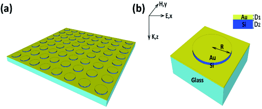 | ||
| Fig. 1 (a) Proposed periodic single-frequency absorber. (b) Schematic of the unit cell of the absorber, consisting of the Au circle (yellow) on the top, the dielectric Si layer (blue) in the middle, the Au ground plane (yellow) on the bottom, and a glass substrate. The structural parameters are: D1 = 0.25 μm, D2 = 2 μm, and R = 18.5 μm. | ||
According to the multiple reflection and interference theory, the absorptance can be calculated as A(ω) = 1 − R(ω) − T(ω) = 1 − |S11(ω)|2 − |S21(ω)|2, where A(ω), T(ω) = |S21(ω)|2, and R(ω) = |S11(ω)|2 are the absorptance, transmittance, and reflectance, respectively.41,42 The transmittance T(ω) is close to zero in the working range because of the existence of the bottom Au plane. Therefore, the absorptance can be simplified to
| A(ω) = 1 − R(ω) = 1 − |S11(ω)|2 | (1) |
Furthermore, S11 depends on the equivalent impedance of the MIM and can be defined as
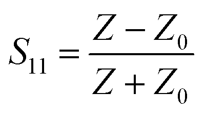 | (2) |
 is the impedance of free space and
  represents the equivalent impedance of MIM. Here, ε0, μ0, ε1, and μ1 are the space permittivity, space permeability, equivalent permittivity, and equivalent permeability, respectively. It can be seen from Fig. 2(a) that the absorptance is as high as 99.97% at 1.36 THz and S11 reaches its minimum value of 0, which is consistent with formula (1). Fig. 2(b) and formula (2) could explain why the value of S11 is so small at the resonance frequency. At 1.36 THz, the imaginary part of the equivalent impedance of MIM is zero and the real part is close to 1. In other words, Z is approximately equal to Z0, so the impedance of MIM and free space are matched, which means that in the ideal case the electromagnetic wave can completely propagate from free space into the MIM without reflection.
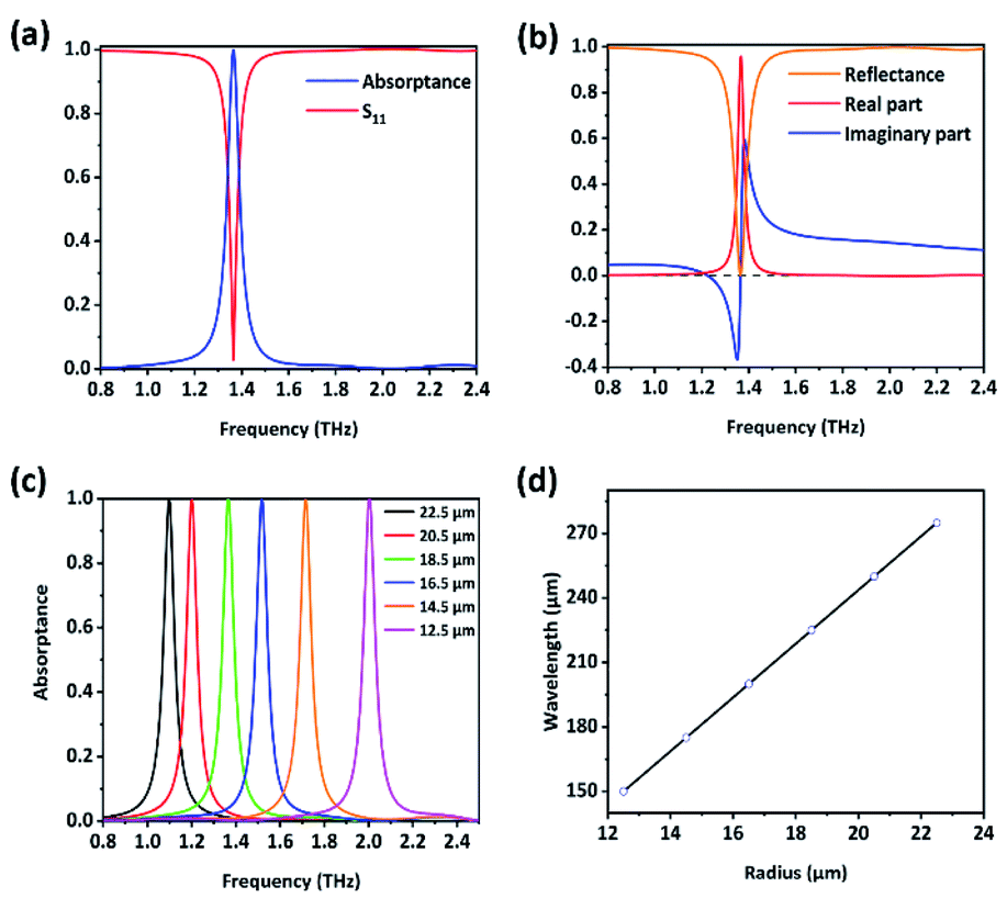 | ||
| Fig. 2 (a) Absorptance spectra and S11 of the proposed MIM structure under normal incidence. (b) Reflectance spectra and equivalent impedance of the proposed MIM structure. (c) Absorptance spectra for different values of radius. (d) Linear relationship between the resonance wavelength and the radius. | ||
An equivalent circuit model is introduced to quantitatively analyze the position of the absorption peak in a better manner. This model can be expressed as43
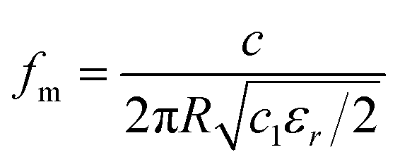 | (3) |
The current distribution and the magnetic field intensity distribution (|H|) in the y = 0 plane are shown in Fig. 3(a) and (d) to get a deeper insight into the physical mechanism of absorption in the designed structure. The current distribution at the interface between dielectric Si and two Au layers is given in Fig. 3(b) and (c). It is clear from Fig. 3(b) that at the resonance frequency, the surface current of the top Au circle is mainly concentrated at the center of the structure and the direction of the surface current on the left side is counterclockwise, while on the right side it is clockwise. So, the magnetic resonance can cancel each other out, and the electric resonance plays a major role here. In contrast, as shown in Fig. 3(c), the surface current on the bottom Au film is also mainly contributed by the center of the circle, but the left side of the current is clockwise and the right side is counterclockwise, which is exactly the opposite of the current direction in the top layer metal. Apart from the anti-parallel current, there is also displacement current in the dielectric Si layer as shown in Fig. 3(a), thus forming the circulating current. Magnetic resonance is excited by the circulating current and results in a strong interaction between the artificial magnetic moment and the magnetic field of the incident light.44–46 Furthermore, it can be seen from Fig. 3(d) that the magnetic resonance here is the first-order resonance, which causes strong charge accumulation. In conclusion, under the combined action of electric resonance and magnetic resonance, the incident electromagnetic energy can be efficiently confined to the absorber and so the absorber achieves a perfect absorption.
 | ||
| Fig. 3 At 1.36 THz, (a) current distribution of the cross-section y = 0. (b) Current distribution in the intersection of the Au circle and the Si circle. (c) Current distribution in the intersection of the Si circle and the Au ground plane. (d) Magnetic field distribution (H) in dielectric Si at plane y = 0. | ||
To expand the application prospect of the absorber, the number of absorption peaks is successfully increased without reducing the absorptance of each peak. As shown in Fig. 4(a), for a single-layer MIM absorber, the blue, orange, and green curves represent different absorption performances when the radius of the MI is 22.5 μm, 16.5 μm, and 12.5 μm, respectively. The frequencies of those three independent peaks are 1.10 THz (peak 1), 1.52 THz (peak 2), and 2.00 THz (peak 3), with absorptance values of 99.98%, 99.85% and 99.95%, respectively. Then, the MI structure with a radius of 12.5 μm is placed on the top of another MI structure whose radius is 16.5 μm forming a double-layer MIMIM absorber. As shown in Fig. 4(b), this absorber eventually achieves perfect absorption at two frequencies, and there is almost no change for peak 2 and peak 3 after they are combined. Furthermore, as shown in Fig. 4(c), three absorption peaks are gained by stacking three MI structures, whose radii are 12.5 μm, 16.5 μm, and 22.5 μm, respectively, on the bottom Au film. Moreover, all the peaks remain above 95% for the incident angle changing up to 60°. The physical mechanism of each peak is similar to that of the single-layer MIM absorber, and different layers independently play a role at different resonance frequencies. According to this design idea, absorbers with more absorption peaks are available; however, the number of absorption peaks is finite within a limited frequency range. Importantly, through the comparison of the three graphs in Fig. 4, it can be concluded that when the peaks are at a certain distance from each other, there is absolutely no interaction between different layers and each peak maintains its original position and absorptance. This advantage provides great convenience for the design of multiple-frequency metamaterial absorbers.
 | ||
| Fig. 4 Simulated absorptance spectra for (a) the structure composed of a single MI layer with different radii, (b) the structure composed of two layers with radii of 16.5 μm and 12.5 μm, and (c) the three-layer structure with radii of 22.5 μm, 16.5 μm and 12.5 μm. | ||
Broadband absorber
Through the simple combination of different absorption peaks, the designed absorber has achieved perfect absorption at multiple frequencies, and during the work, it is noticed that two peaks will be coupled together when they are close enough, which lays the foundation for the broadband absorber. Circular truncated cones are utilized instead of circles to make the radius change smoother so that the coupling of different absorption peaks can be stronger. Besides, the thickness of the metal and dielectric layers is optimized to get the highest absorptance. The structure of the broadband absorber is shown in Fig. 5(a) and (b), and the structure dimensions are listed as follows: L2 = 45 μm, L1 = 22.5 μm, P = 55 μm, H1 = 0.25 μm, H2 = 0.875 μm, and H = 50.625 μm. Details of the FDTD algorithm, such as the boundary conditions, mesh accuracy, automatic shutdown and running time are the same as those of a single MIM absorber in Fig. 1. As shown in Fig. 5(c), broadband absorption is obtained from 1.2 to 2 THz with the average absorptance higher than 99% in the case of vertical incidence, which explicitly presents an excellent broadband property. The completely centrosymmetric structure makes the absorber insensitive to the TE and TM linear polarization. Moreover, it is noted from Fig. 5(d) that the variation of the incident angle has little effect on the absorptance when the incident angle is varied from 0° to 45°, and the average absorptance is still over 85% when the incident angle adds up to 60°. | ||
| Fig. 5 (a) Three-dimensional illustration of the simulated absorber. (b) Schematic diagram of an absorber unit cell. (c) Absorption spectra of the multiple-layer circular truncated cone metamaterial absorber for plane wave of TM polarization and TE polarization under vertical incidence. (d) Absorptance of the broadband absorber at four different incident angles: 0°, 30°, 45°, and 60°. | ||
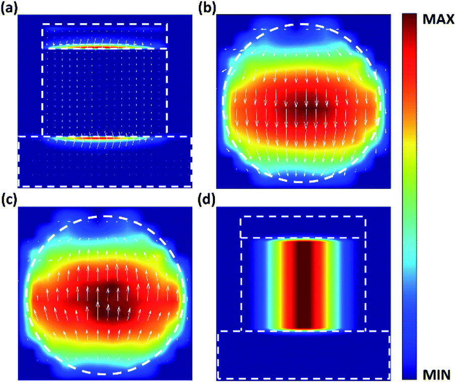
Fig. 6 shows the magnetic field distributions (|H|) at different frequencies at normal incidence taken in cross-section y = 0. It is noticed that the magnetic field is confined to the bottom layers of the circular truncated cones at a smaller frequency and, in other parts, there is no contribution of the magnetic field because the resonance frequency is almost inversely proportional to the average radius of the circular truncated cones. The magnetic field gradually moves toward the top layers as the frequency increases. Because of the slow variation of the radii of the adjacent metal layers, the resonance magnetic field is not limited to two adjacent Si layers but diffuses to several consecutive Si layers, which means several adjacent MIs support the resonance mode together. In other words, magnetic resonance at a lower frequency is primarily related to the excitation of magnetic polariton in several lower layers, which is caused by the electric dipole coupling, and it can be regarded as a hybridized mode of several magnetic polaritons strongly coupled to each other.47,48 Therefore, it is the magnetic resonance rather than the multiple reflections and transmissions in the metamaterial absorbers that is responsible for the effective absorption of incident electromagnetic energy, and the absorption is mainly attributed to the ohmic losses rather than the dielectric losses. The white arrows in Fig. 6 stand for the distribution of the Poynting vector, which reveals how the electromagnetic wave propagates in the absorber before being absorbed. The energy flow spreads downwards in the air along the z-axis without penetrating the absorber and then it rotates and converges into the center of the absorber, where exactly the magnetic field concentrates. This feature appears in many papers32,49 and has been explained with a slow light effect. When light propagates in a waveguide inserted with metal inclusions of various shapes and arrangements, the oscillating current will generate a magnetic field moment, which will have a significant impact on the propagation of light. This kind of structure can slow down the speed of the optical signal, and after the effective thickness of the waveguide is reduced to zero, the waveguide will completely prevent further propagation of the light and capture the light permanently.50 Here, the slow light effect was adopted to illustrate the principle of absorption in the designed structure: the adjacent circular truncated cone layers of the absorber can interact with light as ultra-short vertical waveguides which support the slow light mode at different frequencies so that the incident light of different frequencies can be stopped and captured at different positions.
 | ||
| Fig. 6 Distributions of the magnetic field (H) and the Poynting vector (white arrows) for the absorber in cross-section y = 0 at different frequencies: (a) 1.20 THz, (b) 1.38 THz, (c) 1.64 THz, and (d) 2.00 THz. | ||
The distributions of the electric field (|E|2) in the plane y = 0 at 1.2 THz are shown in Fig. 7(a). Strong enhancement of the electric field is stimulated at specific layers of the absorber which indicates the excitation of the electric resonance. Thus, in this resonance mode, both electric and magnetic resonances exist. Furthermore, the x-component and the z-component of the electric field intensity (|Ex|2, |Ez|2) at 1.2 THz are monitored in Fig. 7(b) and (c), and it is obvious that the x-component is concentrated in the air gap outside the circular truncated cones, while the z-component is concentrated in the dielectric layers (|Ez|2 > |Ex|2). To explore the physical mechanism in depth, the distribution of the real part of the electric field (real(Ez)) at 1.2 THz is displayed in Fig. 7(d). It is identified that opposite charges accumulate on the outside of the circular truncated cones, and it also indicates the existence of the electric dipole resonance, which is related to the localized surface plasmon resonance excited at the metal/dielectric interface.51 At 1.2 THz, the y-component and the z-component of the real part of the electric field (real(Ey), real(Ez)) are demonstrated in Fig. 7(e) and (f) at plane z = 10 μm, where the electric field is concentrated. This suggests the formation of a circular, antisymmetric current in different metal layers which generates the magnetic dipole response.44,52 In short, the physical mechanism of the near-perfect absorption originates from the electric dipole resonance caused by the local surface plasmon resonance and the magnetic dipole resonance between different metal layers.
 | ||
| Fig. 7 At 1.2 THz, (a) distributions of the electric field (|E|2) in the plane y = 0. Distributions of the (b) x-component of the electric field (|Ex|2) and (c) z-component of the electric field (|Ez|2) in the plane y = 0. (d) Distributions of the z-component electric field (real (Ez)) in the plane y = 0. Distributions of the (e) y-component electric field (real (Ey)) and (f) the z-component electric field (real (Ez)) at the metal/dielectric interface (z = 10 μm). | ||
It has been proved that multiple MI layers with different radii can interact with the incident electromagnetic wave and capture it at different frequencies. This attribute allows the structures of the absorbers to be flexibly designed to meet the actual needs. The top layers of the broadband absorber work at high frequencies, and if they are removed, the absorption band will be shorter accordingly. As shown in Fig. 8(a), several MI layers are taken away sequentially from top to bottom, and the absorption band of the 35-layer, 30-layer, and 25-layer absorbers becomes narrower and narrower, but the absorption at low frequencies is not affected. The reorganization of the structures can also occur between a single-frequency absorber and a broadband absorber. Cutting out part of the 45-layer broadband absorber (from the eleventh to the thirty-fifth layer counting from the top to the bottom, structure 1) and stacking them on top of the MIM structure (structure 2), the recombined absorber realizes the combined absorption effect of the two structures, as shown in Fig. 8(b). More importantly, after reorganization, the absorption band of each structure maintains its original position and excellent absorptance without interaction. It can be illustrated from Fig. 8(b) that as the radius of structure 2 increases, the corresponding single-frequency absorption peak will have a redshift, while the broadband absorption is almost unaffected. This flexible design method provides vast prospects for the practical application of the designed absorber.
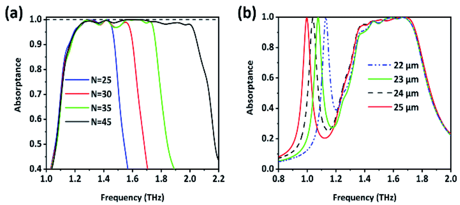 | ||
| Fig. 8 (a) Simulated absorption when N in Fig. 5(a) changes with the other parameters fixed, where N represents the number of MI layers stacked from bottom to top. (b) Combination of single-frequency absorption and broadband absorption as well as the influence of changing the radius of the former. | ||
Conclusions
In conclusion, this paper provides a flexible method to design absorbers, which also has the excellent properties of wide angle and insensitivity to TE and TM waves. The absorptance of the designed MIM absorber is almost 100% at a single frequency and then the physical mechanism is discussed through the current distributions. An absorptance formula is obtained through the impedance matching theory which shows excellent linearity between the wavelength of the peak and the radius of the MI structure. Based on that, multiple-frequency absorption is obtained by stacking several MI layers together, and each peak maintains its original position and absorptance higher than 99%. Furthermore, broadband absorption with the average absorptance exceeding 99% from 1.2 to 2 THz is realized by the stacked Ml layers. The physical mechanism is discussed in detail through several physical images, including the magnetic field distribution, Poynting vector distribution, and electric field distribution. The presented absorbers and the design idea have a promising application prospect and could provide certain references for programmable metamaterials and the design of absorbers in other bands.Conflicts of interest
There are no conflicts to declare.Acknowledgements
This work was sponsored by the National Natural Science Foundation of China (No. 61805127), the Natural Science Foundation of Shandong Province, China (No. ZR2019BF014), the Fundamental Research Funds of Shandong University (No. 2018TB002), the China Postdoctoral Science Foundation funded project (No. 2015M582073), and the Postdoctoral Innovation Program of Shandong Province (No. 201602017).Notes and references
- J. B. Pendry, A. J. Holden, D. J. Robbins and W. J. Stewart, J. Phys.: Condens. Matter, 1998, 10, 4785–4809 CrossRef CAS.
- J. B. Pendry, A. J. Holden, D. J. Robbins and W. J. Stewart, IEEE Trans. Microwave Theory Tech., 1999, 47, 2075–2084 CrossRef.
- D. R. Smith, W. J. Padilla, D. C. Vier, S. C. Nemat-Nasser and S. Schultz, Phys. Rev. Lett., 2000, 84, 4184–4187 CrossRef CAS.
- E. Verhagen, R. de Waele, L. Kuipers and A. Polman, Phys. Rev. Lett., 2010, 105, 223901 CrossRef.
- R. A. Shelby, D. R. Smith and S. Schultz, Science, 2001, 292, 77–79 CrossRef CAS PubMed.
- D. R. Smith, J. B. Pendry and M. C. K. Wiltshire, Science, 2004, 305, 788–792 CrossRef CAS PubMed.
- U. Leonhardt, Science, 2006, 312, 1777–1780 CrossRef CAS PubMed.
- D. Schurig, J. J. Mock, B. J. Justice, S. A. Cummer, J. B. Pendry, A. F. Starr and D. R. Smith, Science, 2006, 314, 977–980 CrossRef CAS.
- R. Liu, C. Ji, J. J. Mock, J. Y. Chin, T. J. Cui and D. R. Smith, Science, 2009, 323, 366–369 CrossRef CAS PubMed.
- A. W. M. Lee and Q. Hu, Opt. Lett., 2005, 30, 2563–2565 CrossRef.
- H. Tao, E. A. Kadlec, A. C. Strikwerda, K. B. Fan, W. J. Padilla, R. D. Averitt, E. A. Shaner and X. Zhang, Opt. Express, 2011, 19, 21620–21626 CrossRef CAS.
- F. Ali and S. Aksu, Materials, 2020, 13, 1–9 Search PubMed.
- W. Li, Z. J. Coppens, L. V. Besteiro, W. Y. Wang, A. O. Govorov and J. Valentine, Nat. Commun., 2015, 6, 8379 CrossRef CAS.
- T. Frank, O. Buchnev, T. Cookson, M. Kaczmarek, P. Lagoudakis and V. A. Fedotov, Nano Lett., 2019, 19, 6869–6875 CrossRef CAS.
- Y. H. Zhu, S. Vegesna, V. Kuryatkov, M. Holtz, M. Saed and A. A. Bernussi, Opt. Lett., 2012, 37, 296–298 CrossRef.
- Y. Xiao, J. Zhang, J. H. Yu, H. Z. Dong, Y. Y. Wei, Y. H. Lu, Y. C. Zhong, W. T. Qiu, J. L. Dong, H. H. Lu, H. Y. Guan, J. Y. Tang, W. G. Zhu and Z. Chen, Opt. Express, 2018, 26, 13759–13772 CrossRef CAS PubMed.
- M. Jeannin, T. Bonazzi, D. Gacemi, A. Vasanelli, S. Suffit, L. H. Li, A. G. Davies, E. Linfield, C. Sirtori and Y. Todorov, Appl. Phys. Lett., 2020, 117, 251102 CrossRef CAS.
- B. Ferguson and X. C. Zhang, Nat. Mater., 2002, 1, 26–33 CrossRef CAS PubMed.
- N. Liu, M. Mesch, T. Weiss, M. Hentschel and H. Giessen, Nano Lett., 2010, 10, 2342–2348 CrossRef CAS.
- X. L. Liu, T. Starr, A. F. Starr and W. J. Padilla, Phys. Rev. Lett., 2010, 104, 207403 CrossRef PubMed.
- N. I. Landy, S. Sajuyigbe, J. J. Mock, D. R. Smith and W. J. Padilla, Phys. Rev. Lett., 2008, 100, 207402 CrossRef CAS PubMed.
- J. Xu, Z. Y. Zhao, H. C. Yu, L. Yang, P. Gou, J. Cao, Y. X. Zou, J. Qian, T. J. Shi, Q. J. Ren and Z. H. An, Opt. Express, 2016, 24, 25742–25751 CrossRef CAS.
- X. P. Shen, T. J. Cui, J. M. Zhao, H. F. Ma, W. X. Jiang and H. Li, Opt. Express, 2011, 19, 9401–9407 CrossRef CAS.
- T. H. Nguyen, S. T. Bui, T. T. Nguyen, T. T. Nguyen, Y. Lee, M. A. Nguyen and D. L. Vu, Adv. Nat. Sci.: Nanosci. Nanotechnol., 2014, 5, 025013 CAS.
- H. L. Dang, V. C. Nguyen, D. H. Le, H. T. Nguyen, M. C. Tran, D. T. Le and D. L. Vu, J. Nonlinear Opt. Phys. Mater., 2017, 26, 1943–1947 CrossRef.
- H. Tao, C. M. Bingham, D. Pilon, K. B. Fan, A. C. Strikwerda, D. Shrekenhamer, W. J. Padilla, X. Zhang and R. D. Averitt, J. Phys. D: Appl. Phys., 2010, 43, 225102 CrossRef.
- P. Fu, F. Liu, G. J. Ren, F. Su, D. Li and J. Q. Yao, Opt. Commun., 2018, 417, 62–66 CrossRef CAS.
- C. Du, D. Zhou, H. H. Guo, Y. Q. Pang, H. Y. Shi, W. F. Liu, J. Z. Su, C. Singh, S. Trukhanov, A. Trukhanov, L. Panina and Z. Xu, Nanoscale, 2020, 12, 9769–9775 RSC.
- Y. H. Guo, L. S. Yan, W. Pan, B. Luo and X. G. Luo, Plasmonics, 2014, 9, 951–957 CrossRef CAS.
- X. W. Li, H. J. Liu, Q. B. Sun and N. Huang, Photonics Nanostruct., 2015, 15, 81–88 CrossRef.
- J. Zhang, X. Wu, L. Liu, C. Huang, X. Chen, Z. Tian, C. Ouyang, J. Gu, X. Zhang, M. He, J. Han, X. Luo and W. Zhang, Opt. Express, 2019, 27, 25595–25602 CrossRef CAS PubMed.
- Y. X. Cui, K. H. Fung, J. Xu, H. J. Ma, Y. Jin, S. L. He and N. X. Fang, Nano Lett., 2012, 12, 1443–1447 CrossRef CAS.
- Y. J. Kim, Y. J. Yoo, K. W. Kim, J. Y. Rhee, Y. H. Kim and Y. Lee, Opt. Express, 2015, 23, 3861–3868 CrossRef CAS.
- T. J. Cui, M. Q. Qi, X. Wan, J. Zhao and Q. Cheng, Light: Sci. Appl., 2014, 3, e218 CrossRef.
- J. Shabanpour, J. Mater. Chem. C, 2020, 8, 7189–7199 RSC.
- J. Shabanpour, S. Beyraghi and A. Cheldavi, Sci. Rep., 2020, 10, 1–14 CrossRef PubMed.
- J. Shabanpour, Ann. Phys., 2020, 532, 2000321 CrossRef.
- J. Shabanpour, S. Beyraghi and H. Oraizi, Sci. Rep., 2020, 10, 1–8 CrossRef.
- Y. Y. Wang, Z. Q. Chen, D. Y. Xu, Z. Yi, X. F. Chen, J. Chen, Y. J. Tang, P. H. Wu, G. F. Li and Y. G. Yi, Results Phys., 2020, 16, 102951 CrossRef.
- M. A. Ordal, R. J. Bell, R. W. Alexander, L. L. Long and M. R. Querry, Appl. Opt., 1987, 26, 744–752 CrossRef CAS.
- L. Zhao, H. Liu, Z. H. He and S. K. Dong, Opt. Commun., 2018, 420, 95–103 CrossRef CAS.
- C. C. Li, B. S. Xie, J. Chen, Z. X. He, Z. S. Chen and Y. Long, Energy Convers. Manage., 2019, 183, 633–644 CrossRef CAS.
- J. Zhou, E. N. Economon, T. Koschny and C. M. Soukoulis, Opt. Lett., 2006, 31, 3620–3622 CrossRef.
- W. Cai, U. K. Chettiar, H. K. Yuan, V. C. de Silva, A. V. Kildishev, V. P. Drachev and V. M. Shalaev, Opt. Express, 2007, 15, 3333–3341 CrossRef PubMed.
- L. Qiu, S. M. Wang, H. Liu, T. Li, S. N. Zhu and X. Zhang, J. Opt. Soc. Am. B, 2011, 28, 1655–1660 CrossRef CAS.
- B. X. Zhang, Y. H. Zhao, Q. Z. Hao, B. Kiraly, I. C. Khoo, S. F. Chen and T. J. Huang, Opt. Express, 2011, 19, 15221–15228 CrossRef CAS PubMed.
- N. Liu, H. C. Guo, L. W. Fu, S. Kaiser, H. Schweizer and H. Giessen, Adv. Mater., 2007, 19, 3628 CrossRef CAS.
- N. Liu, L. W. Fu, S. Kaiser, H. Schweizer and H. Giessen, Adv. Mater., 2008, 20, 3859 CrossRef CAS.
- H. Xiong, J. S. Hong, C. M. Luo and L. L. Zhong, J. Appl. Phys., 2013, 114, 064109 CrossRef.
- K. L. Tsakmakidis, A. D. Boardman and O. Hess, Nature, 2007, 450, 397–401 CrossRef CAS.
- B. Zhang, Y. Zhao, Q. Hao, B. Kiraly, I. C. Khoo, S. Chen and T. J. Huang, Opt. Express, 2011, 19, 15221–15228 CrossRef CAS.
- V. A. Podolskiy, A. K. Sarychev and V. M. Shalaev, J. Nonlinear Opt. Phys. Mater., 2002, 11, 339 CrossRef.
| This journal is © The Royal Society of Chemistry 2021 |