
 Open Access Article
 This Open Access Article is licensed under a Creative Commons Attribution-Non Commercial 3.0 Unported Licence
Hafnium–zirconium oxide interface models with a semiconductor and metal for ferroelectric devices†
Kisung
Chae
 ab,
Andrew C.
Kummel
*a and
Kyeongjae
Cho
*b
ab,
Andrew C.
Kummel
*a and
Kyeongjae
Cho
*b
aDepartment of Chemistry and Biochemistry, University of California San Diego, La Jolla, CA, USA. E-mail: akummel@ucsd.edu
bDepartment of Materials Science and Engineering, The University of Texas at Dallas, Richardson, TX, USA. E-mail: kjcho@utdallas.edu
First published on 29th June 2021
Abstract
Density functional theory (DFT) is employed to investigate ferroelectric (FE) hafnium–zirconium oxide stack models for both metal–insulator–metal (MIM) and metal–insulator–semiconductor (MIS) structures. The role of dielectric (DE) interlayers at the ferroelectric interfaces with metals and semiconductors and the effects of thickness scaling of FE and DE layers were investigated using atomic stack models. A high internal field is induced in the FE and DE layers by the FE polarization field which can promote defect generation leading to limited endurance. It is also shown that device operation will be adversely affected by too thick DE interlayers due to high operating voltage. These DFT models elucidate the underlying mechanisms of the lower endurance in experimental MIS devices compared to MIM devices and provide insights into the fundamental mechanisms at the interfaces.
Introduction
Hafnium–zirconium oxide (HZO) has a key role in next-generation electronic device applications at both the front- and the back-end such as ferroelectric field effect transistors (FeFETs) for nonvolatile memory.1 HZO is a promising new material due to its CMOS-compatibility, scalability, and versatility in electric characteristics ranging from ferroelectric (FE), antiferroelectric (AFE) to dielectric (DE). Experimental and theoretical investigations of HZO have provided a fundamental understanding on the correlation between the crystalline phases and the electrical characteristics of HZO films, which facilitates the optimization of device processing for better performance.2–5 In novel HZO-based FE devices, the HZO films are interfaced with metals and semiconductors, and their interfaces are known to be the source of device variability and reliability challenges.6 However, the relationships between the atomic-scale interface properties and the electric characteristics leading to defect formation and degradation are not well established.Endurance is a key metric for memory applications as it refers to how many times information can be written and erased in a device. Current FeFETs, in metal–insulator–semiconductor (MIS) geometry with HZO as the insulator, typically have endurance less than 107 cycles for silicon-based devices.7–9 In contrast, current HZO-based metal–insulator–metal (MIM) capacitors can have endurances as high as 1011 cycles.10,11 While the main difference is the underlying substrate on which HZO is grown (i.e., semiconductor for MIS and metal for MIM), the detailed nature of semiconductor–HZO and metal–HZO interfaces are not known with fundamental understanding at the atomic scale. The lack of fundamental understanding is due to the limited experimental data for the parameterization of kinetic Monte Carlo simulations to provide projected endurance performance.
It is known that the loss of ferroelectricity of HZO films is correlated with the accumulation of defects (e.g., interface trap states with Dit) as a result of repeated polarization switching.7 It is also known that DE interlayers are formed at the interfaces (semiconductor–HZO and metal–HZO) during the device fabrication, and that the interlayers at semiconductor–HZO interfaces may help reduce defect formation and increase endurance in MIS devices.7 However, it is not clearly understood how the interlayers improve the semiconductor–HZO interface with reduced Dit and enhanced endurance nor how to optimize the interlayers for improved endurance when the thicknesses of the ferroelectric and interlayers are scaled.
In the present study, density functional theory (DFT) calculations are employed to investigate the effects of contact materials with the FE layer and their scaling behaviour in MIM and MIS models. It is found that when FE layers directly contact the metal electrodes in MIM, the internal field buildup is negligible due to the efficient depolarization charge at the metal contact. However, DE interlayer formation at the FE interfaces in MIM or MIS structures induces significant polarization and depolarization fields within the FE and DE layers, indicating a complex role of DE interlayers. Specifically, bond strains accompanied by FE polarization switching may be relieved at FE–substrate interfaces by DE interlayers since the more symmetric bonds of the interlayers remain stable compared to the direct contact of the FE phase with either a metal or a semiconductor. Conversely, the insertion of sub-nanometer DE interlayers introduces additional FE–DE interfaces and consequent electrostatic interactions, which generates large internal fields in both the FE and DE layers. The high fields in FE and DE layers are expected to induce defects at the interfaces, and it is hypothesized that the polarization switching will drive the defects into HZO layers leading to short endurance. To assess the role of FE and DE layer thicknesses in the MIS stack endurance, a systematic modeling study is performed with varying thicknesses of FE and DE layers in the MIS stack structures. The thickness scaling studies of both FE and DE reveal that the magnitude of the FE internal field depends on the FE layer thickness consistent with a scaling limit of about 2 nm of the FE layer.12 More importantly, the interlayer DE thickness is also limited by the depolarization field strength in the lower thickness limit as well as the electrostatic control of the channel by the FE layer through the DE layer in the higher thickness limit. A too thin of a DE interlayer has very high depolarization field strength leading to dielectric breakdown and is hypothesized to lead to defect formation. Conversely, for thicker DE layers, device operation voltage will increase due to an enhanced screening of DE and the correspondingly reduced electrostatic control of the semiconductor channel. The findings in this work provide critical insights into the role of the interlayer DE at the semiconductor–HZO interface.
Computational details
A series of atomic-scale MIM and MIS stack models were generated for FE HZO to investigate the effects of polarization switching on electrostatic interactions and to determine the internal fields due to dipoles in the FE layer. These simple stack models were compared to stack models with interlayer DE at semiconductor–HZO and metal–HZO interfaces, representing practical MIM FE capacitors and MIS FeFETs. A vacuum padding with a thickness of 2 nm was added to minimize the interactions between periodic images, and dipole correction was applied in the middle of the vacuum region to eliminate any field within the vacuum region. Face-centered cubic nickel (Ni) and silicon (Si) were used to represent a metal electrode and a semiconductor channel. An orthorhombic phase of HZO with a space group of Pca21 was employed as a FE material with its polarization aligned either up (+z) or down (−z). Note that HZO films are typically grown along (111), but stack models in this study were generated along (001) for the sake of simplicity. The development of the interface models along the (111) orientation would be challenging due to the larger supercell size and much more complex interfacial bonding especially for the low-symmetry Pca21 phase. It is hypothesized that the electrostatic effects should remain the same qualitatively; however, the polarization vector along the [001] direction in the (111) HZO film is tilted with respect to the growth direction; therefore, the polarization directed at the interface for (111) HZO films will be only 58% of the polarization along [001] so the electrostatic interfacial free energies will be slightly smaller. The atoms in the HZO layer had to be frozen to prevent dipoles from rotating to the side.13,14 In all the models in this study, bridging O atoms at the interfaces were allowed to relax and other atoms were fixed at their bulk equilibrium positions. The validity of relaxing just one layer of interfacial O atoms was checked by allowing additional layers of interfacial atoms to relax for a subset of the calculations. As shown in Fig. S1,† a single layer of atoms being allowed to relax is sufficient for the purpose of the current study to investigate the isolated effects of electrostatic interactions (see the ESI for detailed discussion†). The effects of DE interlayers were investigated by adding a cubic HZO (space group of Fm![[3 with combining macron]](https://www.rsc.org/images/entities/char_0033_0304.gif) m) layer at the interfaces of MIM and MIS stack models. Here, the cubic HZO was used to model the electrostatic role of any DE interlayers such as SiOx at the HZO–Si interface and TiON at the HZO–TiN interface. The cubic phase was used, instead of the ground state monoclinic P21/c phase, because its high symmetry minimizes bond strains. This can be seen as the best-case scenario where the electrostatic effects can be isolated without bond strain. The validity and additional advantages of using the cubic phase are described in the ESI.† The atomic positions in the DE layer were frozen as well to prevent relaxation to lower energy states (e.g., tetragonal P42/nmc phase). The lattice parameters of all the materials along the in-plane directions, i.e., x and y, were fixed at the equilibrium values of the orthorhombic HZO phase; therefore, other phases are strained to match those values.
m) layer at the interfaces of MIM and MIS stack models. Here, the cubic HZO was used to model the electrostatic role of any DE interlayers such as SiOx at the HZO–Si interface and TiON at the HZO–TiN interface. The cubic phase was used, instead of the ground state monoclinic P21/c phase, because its high symmetry minimizes bond strains. This can be seen as the best-case scenario where the electrostatic effects can be isolated without bond strain. The validity and additional advantages of using the cubic phase are described in the ESI.† The atomic positions in the DE layer were frozen as well to prevent relaxation to lower energy states (e.g., tetragonal P42/nmc phase). The lattice parameters of all the materials along the in-plane directions, i.e., x and y, were fixed at the equilibrium values of the orthorhombic HZO phase; therefore, other phases are strained to match those values.
DFT was employed to investigate interface atomic structures, total energies and electronic structures. A plane-wave basis set with a kinetic energy cutoff of 400 eV was used to represent electron wave functions, and the projector augmented wave method was used for the pseudopotential core part.15 The Perdew–Burke–Ernzerhof16 exchange–correlation functional was employed for Kohn–Sham Hamiltonian. The Monkhorst–Pack17 scheme was used for Brillouin zone sampling on a 6 × 6 × 1 grid. Convergence criteria for self-consistent field and ionic relaxation were chosen as 10−4 meV and 1 meV Å−1, respectively. All the DFT calculations were performed by using the Vienna Ab initio Software Package.18,19
Results and discussion
Fig. 1 shows MIM capacitor models with two possible FE polarization orientations, i.e., up and down. The 2 nm-thick FE layer in direct contact with the metal electrodes (Fig. 1a) is compared with the FE in MIM stacks with DE interlayers added between the FE layer and metal electrodes (Fig. 1b). For the direct contact interface, FE potential profiles along the stack are flat, i.e., no internal field, for both polarization directions since the metal electrodes efficiently depolarize the FE polarization fields. In contrast, when DE interlayers, analogous to the TiON interlayer, are inserted at the FE–metal interfaces, potential values at both interfaces are quite different from each other, generating a significant internal field within the FE layer as well as within the DE layers. The magnitude of the polarization field for the 2 nm FE layer is ∼20 MV cm−1, which exceeds a breakdown voltage of bulk HfO2 (∼13 MV cm−1).20 The large field induced by the DE interlayer would create reliability problems during device operation such as defect formation decreasing the endurance of the MIM device. The effects of individual DE layers on top and bottom interfaces in MIM are shown in Fig. S2 in the ESI.†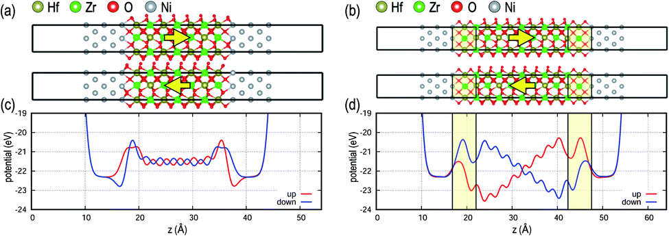 | ||
| Fig. 1 MIM capacitor models with and without DE interlayers. (a) FE HZO (2 nm) with polarization up and down is in direct contact with metal electrodes. (b) One unit cell (0.5 nm) of DE HZO, marked with a yellow box, serves as a buffer layer between FE and metal electrodes. (c and d) Potential profiles along the stack (z direction) for each model with polarization up and down are shown. Metal electrodes are capable of accommodating excess charges at the interfaces due to dipoles resulting in a flat potential profile inside the FE layer, while a significant potential gradient is induced by the DE interlayer. | ||
The MIS FeFET models with the same FE thickness of 2 nm are shown in Fig. 2, and the field strength within the FE layer shows a different behavior than those of MIM models. Unlike the MIM stacks, the potential profiles are not symmetric between the polarization states due to the asymmetry of Si–HZO and Ni–HZO interfaces (see Fig. 2c). For the MIS without DE interlayers (Fig. 2a), the polarization up state shows a finite gradient in the potential profile, while a negligible potential gradient is shown for the polarization down state. This is attributed to several factors. First, semiconductors are less polarizable than metals and have a lower capability to accommodate charge changes at interfaces. For metal electrodes, excess polarization charge due to the FE material can be compensated for by the large density of states near the Fermi level. Second, electrons are delocalized and bonding is non-directional in metals, providing more flexibility for O atoms at the interface upon polarization switching. Conversely, polarization switching in MIS induces bond strain in Si atoms at the interface and would serve as a source of defect formation near the interface. Third, an interface dipole, marked with an orange arrow at the Si interface in Fig. 2, is formed at the Si–HZO interface because the bonding character of the interfacial Si atoms changes from covalent to half-ionic (i.e., +2 charge state compared to +4 charge state when fully ionic). The interface dipole electrostatically interacts with the FE dipole resulting in asymmetric potential profiles for MIS without the DE interlayer depending on the polarization state.21
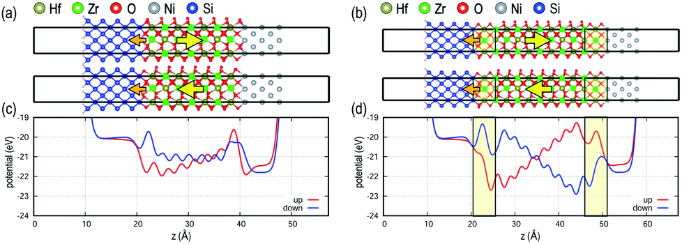 | ||
| Fig. 2 MIS FeFET models with and without DE interlayers. (a) FE HZO (2 nm) with polarization up and down is in direct contact with metal and semiconductor electrodes. (b) One unit cell (0.5 nm) of DE HZO, shown with a yellow box, serves as a buffer layer between FE and the electrodes. (c and d) Potential profiles along the stack (z direction) for each model with polarization up and down are shown. Unlike the MIM case, a potential gradient is observed even when the FE layer is in direct contact with the electrodes. The DE interlayers induce significant internal fields inside the FE layer. | ||
When DE interlayers are added to both MIS interfaces, two profound changes are observed (Fig. 2b). First, the magnitude of the internal field is increased similar to when DE interlayers are added to the MIM stacks. Second, the potential profile transforms from asymmetric to symmetric. The DE interlayers in MIS have two primary effects: (a) due to the electrostatic interactions, the DE interlayers induce a significant internal field in the FE layer. (b) The DE interlayer reduces the bond strains at the interface serving as a buffer layer. The former effect depends significantly on the thicknesses of both FE and DE layers as discussed below.
The individual role of DE interlayers located at the top and bottom interfaces is systematically investigated for MIS as seen in Fig. 3; see Fig. S2† in the ESI for MIM. In contrast to the complete charge compensation of the metals, the internal field increases with the addition of the DE interlayer, but the behavior is asymmetric due to the interface dipole at the Si/oxide interface. For the polarization up case, the increase in the internal field is only seen when the top DE interlayer is added at the FE and metal interface (see “both” and “top” in Fig. 3a), whereas the bottom DE interlayer does not influence the internal field (see Fig. 3a; “bottom” and “none”). Conversely, when the polarization is switched to down as in Fig. 2b, the internal field gradually increases with the addition of the DE interlayers. The pinned interface dipole interacts with the polarization dipole in the FE layer, inducing asymmetry in the electrostatic behavior, as discussed below.
 | ||
| Fig. 3 Potential profiles for MIS stacks with various DE interlayer formations. Polarization (a) up and (b) down. DE is marked with a yellow box, and the FE layer is shown as black dashed lines. Note that the potential values at the top metal electrode and bottom Si channel remain unchanged regardless of the DE interlayer formation. | ||
The presence of a high internal field in the FE layer due to the DE interlayers would adversely affect the device performance especially its endurance. With an internal field, it is hypothesized that a larger number of charged point defects (e.g., oxygen vacancy, VO) would be formed to compensate for the internal field, generating defect trap states within the bandgap and leakage current,22,23 which would drive the device in a fatigue stage.24 In addition, with field cycling, the potential profile is repeatedly reversed, and it is hypothesized that this would promote VO migration, altering the chemical composition of HZO to nonstoichiometric compositions. This may change the relative stability among the polymorphs of HZO, destabilizing the FE phase as the device cycles.
The strength of the field in the FE layer induced by the DE interlayers sensitively depends on the thickness of the FE layer as shown in Fig. 4. The field decreases for thicker FE layers, while the potential levels at both Ni and Si remain unchanged. The internal field is computed from a linear fit of the slope of the potential profile within the FE layer and decreases monotonously with increasing FE thickness. While a smaller FE thickness is desired for low voltage device operation, the results in this study show that the endurance of the device could be compromised due to the adverse effects described above. In sum, there might be a physical limit for FE thickness scaling. This is consistent with most of the FE layers in fabricated devices being typically thicker than 5 nm, and the only report of a sub 3 nm FE HZO film is not in a working device with high endurance.12,25,26
Thickness scaling for DE interlayers with the FE thickness fixed at 2 nm is shown in Fig. 5. The field strength inside the FE is independent of the DE thickness under unbiased conditions, although for a given external bias, the amount of voltage applied to the FE layer will be altered due to the DE thickness. Similar to the FE scaling behavior, the depolarization field inside the DE interlayer decreases with increasing DE thickness. A very thin DE interlayer would very likely induce defect formation thereby limiting endurance.
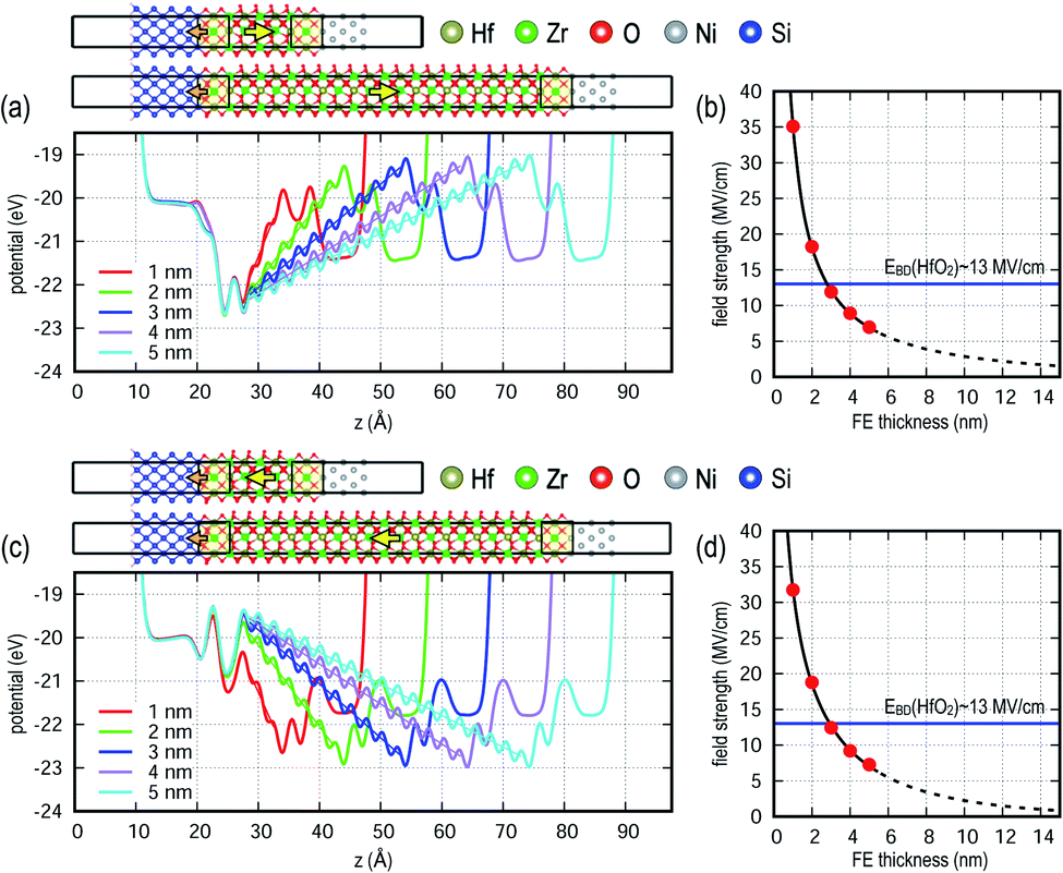 | ||
| Fig. 4 FE thickness scaling in MIS FeFET models with 0.5 nm DE interlayers. Potential profiles with varying FE thickness for polarization (a) up and (c) down. (b and d) The internal field, computed from the slope of the potential profile, is plotted as a function of the FE thickness. Blue horizontal line indicates the breakdown voltage of bulk HfO2.20 | ||
For a FeFET to be successfully used in a non-volatile memory application, Isd–Vsd characteristics must strongly depend on the polarization state in the FE layer, so the change of the potential profile (ΔV) in the Si channel region due to polarization switching is calculated. A memory window, the amount of shift in the Isd–Vsd curve due to polarization switching, is a measure of the potential stability of a device. Fig. 6a shows that ΔV is highest when the Si is closest to the FE layer, and deceases with increasing DE thickness. It also shows that ΔV is primarily a function of the DE thickness and only weakly dependent on the FE thickness, which is because electrostatic effects are primarily induced by the excess charge at the interfaces. When the DE thickness is reduced to a sub-nanometer scale (e.g., 0.5 nm), ΔV rapidly varies to negative values near the interface as shown in Fig. 6b. This is an anomalous behavior resulting from an excessive internal field in thin DE interlayers and may need to be avoided for stable device operation.
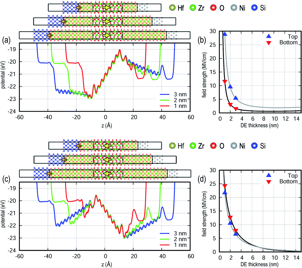 | ||
| Fig. 5 DE thickness scaling in MIS FeFET models. Potential profiles with varying DE interlayer thickness for polarization (a) up and (c) down. (b and d) The internal fields on both top and bottom electrodes (Si and Ni side interfaces, respectively) are computed from the slope of the potential profile in the corresponding regions as a function of the DE thickness. | ||
The different bonding environment of Si at the interface than in the bulk, i.e., half-ionic versus fully covalent, induces an interfacial dipole as discussed above; see the orange arrows at the Si interface in Fig. 2. The interfacial dipole at the Si interface can interact with the polarization dipole in the FE layer, resulting in an asymmetric energy landscape due to the polarization state as shown in Fig. 7a. This is in contrast to MIM capacitors without interface dipole formation, which show a symmetric energy landscapes as seen in Fig. 7b. Note that the polarization switching energy barriers in MIS structures are not identical between up-down and down-up due to the asymmetric energy landscape. Fig. 7c shows that the difference in energy (ΔE) decreases monotonously with the DE interlayer thickness, confirming that the origin of the asymmetry is due to the screened interaction between interfacial and polarization dipoles.
 | ||
| Fig. 6 Potential difference (ΔV) profile due to polarization switching in the semiconductor channel of MIS. On the top, an atomic model with a scale along the z axis is shown. (a) ΔV profile is shown as a function of varying thicknesses of both FE and DE layers. The color of the line corresponds to the DE thickness while the texture of the line corresponds to the FE thickness. Note that the FE thickness only has a small effect on ΔV while the DE thickness has a large effect on ΔV. (b) ΔV profile is shown as a function of DE thickness for a FE thickness of 2 nm. Anomalous behavior near the interface is seen when the DE thickness is 0.5 nm. | ||
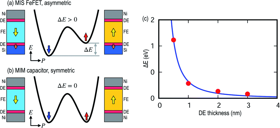 | ||
| Fig. 7 Total energy landscape in MIM and MIS devices. Schematic diagram of energy landscapes as a function of polarization state for (a) an asymmetric MIS FeFET and (b) a symmetric MIM capacitor. (c) The energy difference (ΔE) as a function of DE thickness in MIS with the FE thickness fixed at 2 nm. | ||
The DFT results suggest that thin DE interlayer formation (sub 1 nm) needs to be suppressed to avoid large internal field buildup in the FE layer for better endurance. If a DE layer is present, both the DE and FE layers need to be sufficiently thick to reduce the internal field strengths. For Si devices, DE formation is nearly unavoidable; interfacial oxides are known to form spontaneously at the Si/gate oxide interface21 especially when thermal annealing at an elevated temperature is required to crystalize the as-grown amorphous HZO film. A careful control of the interlayer DE thickness and defect tolerance would be a critical factor for improving the endurance of MIS devices beyond the current cycle limits. The DFT calculations suggest that the following should enhance the endurance: (1) suppressing the interlayer formation by employing a channel less prone to oxidation (e.g., Ge, SiGe or oxide semiconductors), (2) reduction of voltage drop in the DE layer either by employing interlayer materials with a higher k value or (3) by lowering the operating voltage by using ferroelectric subloops to reduce the voltage drop in the DE layer. It is noted that there are several reports of enhanced endurance using oxide semiconductor channels in FeFETs27–30 or Ge MOSCAPs31 consistent with the above suggestions. Note that it is very difficult to quantitatively model any enhanced endurance since this requires a complicated set of kinetic Monte Carlo calculations. The parameters for these kinetic Monte Carlo calculations must come either from DFT calculations of the activation barrier for low density defect formation, which are too computationally intensive to be practical or from detailed experimental data on the temperature dependence of defect formation which does not exist. Therefore, it is only practical to use DFT calculations to suggest better channel materials without being able to give a quantitative estimate of the improvement in endurance. In contrast, a direct interface between HZO and metal electrodes can be relatively easily achieved by suppressing the interlayer DE formation. This finding is consistent with MIM capacitors showing a better endurance of 1011 cycles10,11 than MIS Si FeFETs (107 cycles7–9). By controlling the DE interlayer at metal–HZO, it would be possible to further improve the endurance of MIM devices.
Conclusions
Atomic stack models are developed to elucidate the atomic scale behaviour of semiconductor–HZO and metal–HZO interfaces with detailed atomic and electronic structure information, and the findings from DFT modeling provide insight into the origins of different endurance behaviours of HZO-based FE devices with MIM and MIS structures. DFT calculations show that the MIM structure provides a more flexible bonding environment than MIS structures for the interfacial O atoms to displace upon polarization switching due to the more flexible bond lengths and angles of metal–O compared to Si–O bonds. Furthermore, the FE layer has a large internal field when in contact with a semiconductor since the semiconductor cannot provide a surface compensation charge for the FE polarization. The insertion of DE layers in MIM and MIS structures can reduce bond strains but result in electrostatic interactions, which induce a significantly high internal field both in FE and DE layers, which are hypothesized to promote defect generation and cause FE device degradation. The strength of the induced field is shown to decrease with the increasing thickness of the FE and DE layers, suggesting a physical thickness scaling limit. These findings on FE and DE scaling behaviour provide microscopic understanding to develop an interface engineering strategy to overcome the endurance problems of current HZO FE MIS and MIM devices.Conflicts of interest
There are no conflicts to declare.Acknowledgements
This work was supported by ASCENT, one of six centers in JUMP, a Semiconductor Research Corporation (SRC) program sponsored by DARPA. K. Cho was supported by National Research Foundation (NRF) of Korea by Creative Materials Discovery Program (2015M3D1A1068062) and Nano Materials Technology Development Program (2016M3A7B4909942).Notes and references
- A. I. Khan, A. Keshavarzi and S. Datta, Nat. Electron., 2020, 3, 588–597 CrossRef.
- J. Müller, T. S. Böscke, U. Schröder, S. Mueller, D. Bräuhaus, U. Böttger, L. Frey and T. Mikolajick, Nano Lett., 2012, 12, 4318–4323 CrossRef PubMed.
- R. Materlik, C. Künneth and A. Kersch, J. Appl. Phys., 2015, 117, 134109 CrossRef.
- S. J. Kim, D. Narayan, J.-G. Lee, J. Mohan, J. S. Lee, J. Lee, H. S. Kim, Y.-C. Byun, A. T. Lucero, C. D. Young, S. R. Summerfelt, T. San, L. Colombo and J. Kim, Appl. Phys. Lett., 2017, 111, 242901 CrossRef.
- M. H. Park, Y. H. Lee, H. J. Kim, Y. J. Kim, T. Moon, K. D. Kim, S. D. Hyun, T. Mikolajick, U. Schroeder and C. S. Hwang, Nanoscale, 2018, 10, 716–725 RSC.
- M. H. Park, D. H. Lee, K. Yang, J.-Y. Park, G. T. Yu, H. W. Park, M. Materano, T. Mittmann, P. D. Lomenzo, T. Mikolajick, U. Schroeder and C. S. Hwang, J. Mater. Chem. C, 2020, 8, 10526–10550 RSC.
- W. Xiao, C. Liu, Y. Peng, S. Zheng, Q. Feng, C. Zhang, J. Zhang, Y. Hao, M. Liao and Y. Zhou, Nanoscale Res. Lett., 2019, 14, 254 CrossRef PubMed.
- K.-T. Chen, H.-Y. Chen, C.-Y. Liao, G.-Y. Siang, C. Lo, M.-H. Liao, K.-S. Li, S. T. Chang and M. H. Lee, IEEE Electron Device Lett., 2019, 40, 399–402 CAS.
- K. Chatterjee, S. Kim, G. Karbasian, A. J. Tan, A. K. Yadav, A. I. Khan, C. Hu and S. Salahuddin, IEEE Electron Device Lett., 2017, 38, 1379–1382 CAS.
- R. Cao, Q. Liu, M. Liu, B. Song, D. Shang, Y. Yang, Q. Luo, S. Wu, Y. Li, Y. Wang and H. Lv, IEEE Electron Device Lett., 2019, 40, 1744–1747 CAS.
- M. G. Kozodaev, A. G. Chernikova, E. V. Korostylev, M. H. Park, R. R. Khakimov, C. S. Hwang and A. M. Markeev, J. Appl. Phys., 2019, 125, 034101 CrossRef.
- S. S. Cheema, D. Kwon, N. Shanker, R. dos Reis, S.-L. Hsu, J. Xiao, H. Zhang, R. Wagner, A. Datar, M. R. McCarter, C. R. Serrao, A. K. Yadav, G. Karbasian, C.-H. Hsu, A. J. Tan, L.-C. Wang, V. Thakare, X. Zhang, A. Mehta, E. Karapetrova, R. V. Chopdekar, P. Shafer, E. Arenholz, C. Hu, R. Proksch, R. Ramesh, J. Ciston and S. Salahuddin, Nature, 2020, 580, 478–482 CrossRef CAS PubMed.
- K. Chae, J. Hwang, E. Chagarov, A. Kummel and K. Cho, J. Appl. Phys., 2020, 128, 054101 CrossRef CAS.
- K. Chae, K. J. Cho and A. C. Kummel, in 2020 International Symposium on VLSI Technology, Systems and Applications (VLSI-TSA), IEEE, Hsinchu, Taiwan, 2020, pp. 94–95 Search PubMed.
- G. Kresse and D. Joubert, Phys. Rev. B: Condens. Matter Mater. Phys., 1999, 59, 1758–1775 CrossRef CAS.
- J. P. Perdew, K. Burke and M. Ernzerhof, Phys. Rev. Lett., 1996, 77, 3865–3868 CrossRef CAS PubMed.
- H. J. Monkhorst and J. D. Pack, Phys. Rev. B: Solid State, 1976, 13, 5188–5192 CrossRef.
- G. Kresse and J. Furthmüller, Phys. Rev. B: Condens. Matter Mater. Phys., 1996, 54, 11169–11186 CrossRef CAS PubMed.
- G. Kresse and J. Furthmüller, Comput. Mater. Sci., 1996, 6, 15–50 CrossRef CAS.
- C.-H. Chang and J.-G. Hwu, IEEE Trans. device mater. Reliab., 2009, 9, 215–221 CAS.
- N. Miyata, Materials, 2012, 5, 512–527 CrossRef CAS PubMed.
- J. L. Gavartin, D. Muñoz Ramo, A. L. Shluger, G. Bersuker and B. H. Lee, Appl. Phys. Lett., 2006, 89, 082908 CrossRef.
- P. Broqvist and A. Pasquarello, Appl. Phys. Lett., 2006, 89, 262904 CrossRef.
- M. Pešić, F. P. G. Fengler, L. Larcher, A. Padovani, T. Schenk, E. D. Grimley, X. Sang, J. M. LeBeau, S. Slesazeck, U. Schroeder and T. Mikolajick, Adv. Funct. Mater., 2016, 26, 4601–4612 CrossRef.
- A. Chernikova, M. Kozodaev, A. Markeev, D. Negrov, M. Spiridonov, S. Zarubin, O. Bak, P. Buragohain, H. Lu, E. Suvorova, A. Gruverman and A. Zenkevich, ACS Appl. Mater. Interfaces, 2016, 8, 7232–7237 CrossRef CAS PubMed.
- A. Chouprik, A. Chernikova, A. Markeev, V. Mikheev, D. Negrov, M. Spiridonov, S. Zarubin and A. Zenkevich, Microelectron. Eng., 2017, 178, 250–253 CrossRef CAS.
- H. Ye, J. Gomez, W. Chakraborty, S. Spetalnick, S. Dutta, K. Ni, A. Raychowdhury and S. Datta, in 2020 IEEE International Electron Devices Meeting (IEDM), IEEE, San Francisco, CA, USA, 2020, pp. 28.3.1-28.3.4 Search PubMed.
- S. Dutta, H. Ye, W. Chakraborty, Y.-C. Luo, M. S. Jose, B. Grisafe, A. Khanna, I. Lightcap, S. Shinde, S. Yu and S. Datta, in 2020 IEEE International Electron Devices Meeting (IEDM), IEEE, San Francisco, CA, USA, 2020, pp. 36.4.1-36.4.4 Search PubMed.
- M. Si, A. Murray, Z. Lin, J. Andler, J. Li, J. Noh, S. Alajlouni, C. Niu, X. Lyu, D. Zheng, K. Maize, A. Shakouri, S. Datta, R. Agrawal and P. D. Ye, IEEE Trans. Electron Devices, 2021, 1–5 CAS.
- M. Si, J. Andler, X. Lyu, C. Niu, S. Datta, R. Agrawal and P. D. Ye, ACS Nano, 2020, 14, 11542–11547 CrossRef CAS.
- K.-Y. Chen, Y.-H. Huang, R.-W. Kao, Y.-X. Lin and Y.-H. Wu, in 2018 IEEE Symposium on VLSI Technology, IEEE, Honolulu, HI, 2018, pp. 119–120 Search PubMed.
Footnote |
| † Electronic supplementary information (ESI) available. See DOI: 10.1039/d1na00230a |
| This journal is © The Royal Society of Chemistry 2021 |