DOI:
10.1039/D1NA00198A
(Paper)
Nanoscale Adv., 2021,
3, 4579-4588
Topology design of digital metamaterials for ultra-compact integrated photonic devices based on mode manipulation†
Received
16th March 2021
, Accepted 25th June 2021
First published on 25th June 2021
Abstract
Precise manipulation of mode order in silicon waveguides plays a fundamental role in the on-chip all-optical interconnections and is still a tough task in design when the functional region is confined to a subwavelength footprint. In this paper, digital metamaterials consisting of silicon and air pixels are topologically designed by an efficient method combining 2D finite element method for optical simulations, density method for material description and method of moving asymptotes for optimization. Only around 150 iterations are required for searching satisfactory solutions. Six high-quality and efficient conversions between four TE-polarized modes are achieved in a functional region with footprint 0.645λ2 (center wavelength λ = 1550 nm). Based on asymmetric mode conversion, a reciprocal optical diode with high contrast ratio is further obtained with the optimization starting from TE0-to-TE1 mode converter. Moreover, we successfully design a 1 × 2 demultiplexer with footprint 1.0λ2 and demonstrate a simple mode division multiplexing system with satisfactory performances. Finally, by changing the refractive index to an equivalent value, quasi-3D designs are obtained and the functionalities are validated in 3D simulations for both free-standing and SOI configurations.
1. Introduction
Manipulation of mode order in silicon waveguides has attracted extensive attention in terms of acting as promising building blocks in novel applications, such as on-chip all-optical diodes and mode division multiplexing systems.1–5 Several conventional schemes have been proposed to achieve mode order conversion in waveguides, which include interferometer,6–8 two-dimensional photonic crystal structure,9–13 metasurface,14 deformed silicon waveguide,15 partial etching,16–18 direct waveguide coupling5,19 and sub-wavelength grating coupling.20,21 However, the footprints of the reported photonic devices based on the above mentioned schemes are mostly around 5 to 10 microns and even larger. A compact structure as an essential attribute should be highly emphasized in integrated photonic devices. In recent years, methods involving topology optimization have been put forward in order to reduce the footprint and avoid design obstacles due to the lack of known underlying mechanisms.22–24 The distribution of materials with refractive index contrast inside the compact functional region can be obtained by topology optimization via two distinct strategies: ordinary optimization and objective-first optimization. In ordinary optimization, the problem is to minimize the objective function accounting for the desired mode conversion step by step, while the governing equations, i.e. Maxell's equations, are always satisfied in each iteration.11–13 On the contrary, satisfying of the objective is kept prior to the governing equations in the objective-first strategy, and the optimization is used to find the solution which minimizes the physical residue.25,26 Following these two strategies, the search of optimal material distribution can be performed using ether gradient-based algorithms or non-gradient-based algorithms.27–29 Moreover, from the geometric perspective, the targeted material distributions possess either complex continuous pattern11–13,30 or pixelated pattern (also referred to as metastructure or digital metamaterial).28,29 The description of continuous shape needs additional efforts like the geometric projection method and smoothing method. The pixelated ones with nanoscale pixels are easier to describe in simulation and fabricate in experiment.
Although great efforts have been made toward designing ultra-compact mode converters, precise conversions between all supported mode orders in a single waveguide are rarely reported in the literature.25,31 A pioneer work was reported by Lu et al.25 using an objective-first algorithm. The footprints of functional regions were achieved as 1.55 square vacuum wavelengths with continuous relative permittivity inside. When considering a limiting size of the functional region, i.e. width of the functional region is the same as that of the waveguide, such further reduction of footprint would bring huge challenges in design due to the limited space for light interference.25,26 Meanwhile, the speed of convergence in optimization is another important issue.26 The gradient/sensitivity in gradient-based algorithms can accelerate the optimization process compared with non-gradient-based algorithms (e.g. direct binary search28,32 and particle swarm optimization29), especially in cases with a large amount of design freedom. Recently, machine learning has been adopted to design nanophotonic devices such as a power splitter.33 However, for a large amount of pixels and for such complicated mode conversion functionality, a huge dataset is required and only a purely random dataset may not be sufficient to obtain effective inverse design. Moreover, important applications based on mode conversion, e.g. optical diodes26,32 and mode demultiplexers,34,35 are still being pursued to be achieved in a more highly compact functional region, while major performances like mode purity, insertion loss and contrast ratio are not compromised.
In this paper, ultra-compact integrated digital metamaterials for mode order manipulation, reciprocal unidirectional transmission and mode division multiplexing are demonstrated. Combining finite element method (FEM), density method (DM) and method of moving asymptotes (MMA), we efficiently obtain these high-quality inverse designs in around only 150 iterations. The functional regions of mode converter and optical diode are 0.645λ2 in terms of footprint, while the value of mode division multiplexer is 1.0λ2.
2. Design and method
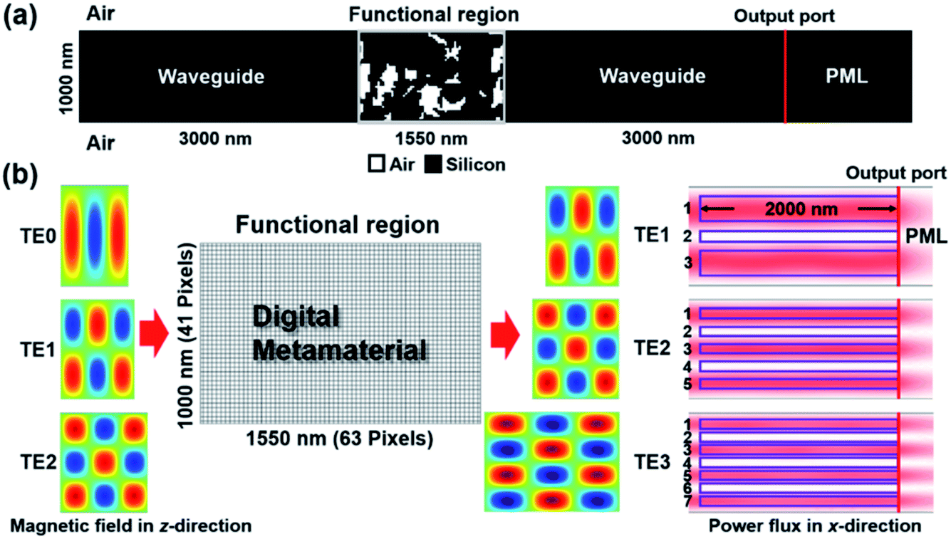
The functional region, consisting of digital metamaterial, is directly integrated with a 1 μm-width multimode silicon slab waveguide surrounded by air. As shown in Fig. 1(a), the functional region is set one center wavelength (1.55 μm) in length and connects two adjacent 3 μm-length waveguides. At the output end, 3 μm-length perfectly matched layers are set to avoid backward reflection. As in the slab waveguide, only TE-polarized (magnetic field perpendicular to the slab) light is considered. We adopt 2D FEM to simulate the optical fields and transmission properties of the proposed device, with input mode profile generated by mode analysis. In 2D simulation, this 1 μm-width silicon slab waveguide (refractive index n = 3.464) can support four modes, i.e. TE0, TE1, TE2 and TE3, with the last one having transmission efficiency less than 0.9 due to the worst confinement. The simulated mode spatial magnetic fields (Hz) are shown in Fig. 1(b). The aim of the pixelated functional region is to precisely manipulate the mode order and further achieve applications in unidirectional transmission and mode division multiplexing.
 |
| | Fig. 1 (a) Schematic of digital metamaterial integrated with silicon waveguide. (b) Magnetic fields and power fluxes of the targeted mode conversions in the waveguide. The functional region made by silicon and air pixels is zoomed in. The integral regions for building the objective function are marked as well. | |
The total footprint of the functional region is set as small as 1 μm × 1.55 μm (0.645λ2), and divided to 41 × 63 pixels. A non-boundary pixel is square with edge length of 25 nm, while a pixel on the boundary is rectangular with edge lengths of 25 nm and 12.5 nm. In each pixel, the material is either silicon or air, forming the required dielectric refractive index contrast. To numerically describe the pattern, the DM36 is adopted, in which the whole digital metamaterial is treated as a single domain. A control variable field 0 ≤ θ ≤ 1 is defined to describe and control the local refractive index with a simple linear relation: n = 1 + θ(3.464 − 1). This variable is evaluated on each mesh node in FEM and, as a consequence, the mesh in the functional region is accordingly set as square to keep the pattern nearly pixelated. In this definition, θ = 0 (θ = 1) refers to air (silicon). To reduce the intermediate values of θ, a projection based on the hyperbolic tangent function37
| | | θ = [tanh(β(θ − θβ)) + tanh(βθβ)]/[tanh(β(1 − θβ)) + tanh(βθβ)] | (1) |
is also introduced, benefiting the targeted binary material design. Here
β and
θβ are slope and projection point, respectively.
Determining the silicon/air pixel pattern in the digital metamaterial is a topology optimization task. In this work, we follow a traditional strategy with a gradient-based MMA algorithm27,38 to fulfil the minimization of the objective function accounting for the targeted device functionality. The control variable θ works as the optimization variable in the MMA process. From an initial guess, θ together with the corresponding dielectric distribution is updated in each iteration based on the sensitivity evaluated by the adjoint method. The physics is exactly held at every step without residual. Then, the silicon/air pixel pattern gradually approaches the optimal design. For mode conversion, we define the objective function based on the spatial integrals of forward power flux (in x-direction) near the output port. The power flux distributions of the perfect expected modes, i.e. TE1, TE2 and TE3 in a silicon waveguide, are shown in Fig. 1(b) and the integral regions (denoted as Ai) are highlighted by solid boxes. The objective function to be minimized is simply written as
| |  | (2) |
where center wavelength
λ = 1550 nm and
wi is the signed weight of each integral to ensure the conversion to the expected mode order. The number of iterations in the MMA process is below 200 to obtain a reasonable solution for all designs shown in this paper. Afterwards, a post-binarization process is adopted to regulate the digital metamaterial with only silicon and air pixels. In experiments, E-beam lithography and reactive ion etching are expected to be used to fabricate the topologically designed digital metamaterials in which the air pixels are only a few tens of nanometers in size.
32,33
3. Results and discussion
3.1 Mode order manipulation
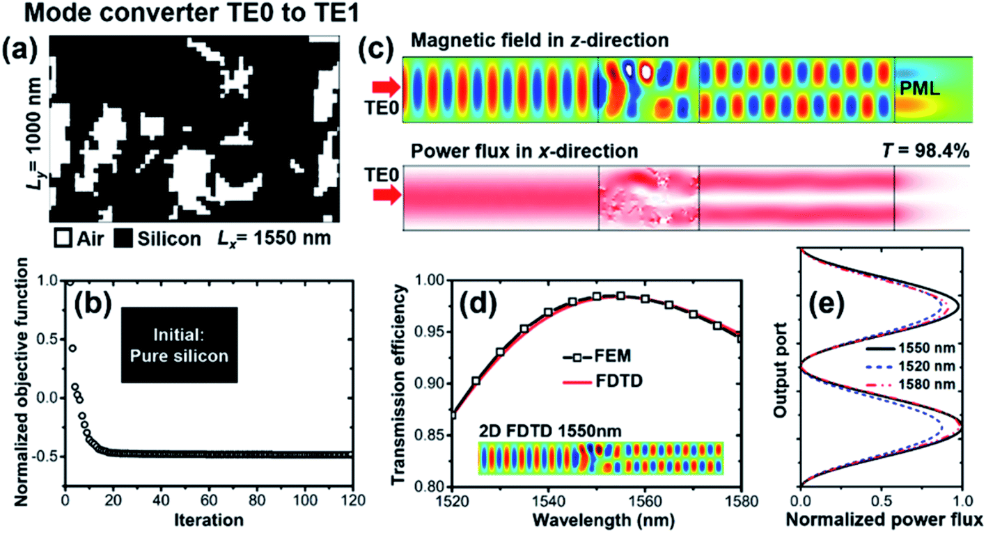
First, we start from the lowest mode order conversion in the silicon slab waveguide, namely from TE0 to TE1. The digital metamaterial obtained by topology optimization is shown in Fig. 2(a). The black and white pixels are silicon and air, respectively. The simulation is performed by 2D FEM with refractive index of silicon n = 3.464. This setting corresponds to infinite thickness of the slab waveguide. The trivial material absorption of silicon around 1550 nm is not considered. Since the initial shape determines the final shape in most topology optimizations, we adopt the simplest initial guess that the digital metamaterial is just pure silicon without air (θ = 1). From the convergence diagram shown in Fig. 2(b), the objective function drops rapidly in the initial stage and converges to a solution after around 120 MMA iterations, reflecting MMA together with density model as an efficient algorithm. With TE0 mode imported from the left port, the magnetic field (z-direction) and power flux (x-direction) simulated at center wavelength 1550 nm are plotted in Fig. 2(c). A high-quality conversion from TE0 to TE1 can be observed. From the power flux point of view, after the TE0 mode arrives at the functional region in forward direction, the single-peak power flux gradually divides into two peaks due to the scattering induced by the air pixels in the functional region. The double-peak power flux remains stable in the subsequent silicon waveguide. If analogically considering the digital metamaterial as a small splitter and interferometer, a π phase difference between upper and lower paths is achieved at the right-hand end of the functional region. Fig. 2(d) plots the parabola-like transmission spectra from 1520 nm to 1580 nm (60 nm operational bandwidth). The transmission efficiency is 98.4% at center wavelength and the minimum value is larger than 87.0% at 1520 nm. Based on the pattern obtained in FEM, we built this digital metamaterial with silicon waveguide in 2D finite-difference time domain (FDTD) as a validation. Consistent results are shown in Fig. 2(d). Moreover, the output flux is measured on the output ports. At center wavelength, the shapes of output fluxes satisfactorily reproduce the shapes of standard TE1 modes. At 1520 nm and 1580 nm, only small distortions unavoidably occur. The results indicate that the performance of the digital metamaterial obtained from optimization at only center wavelength is acceptable and no additional optimization for expanding operational bandwidth is required.
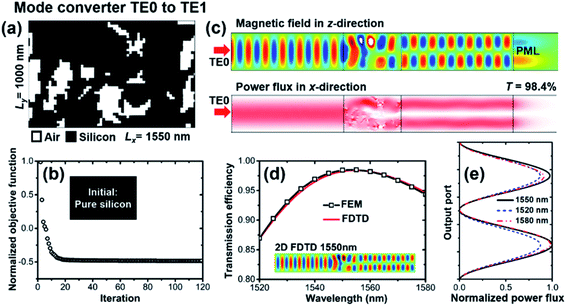 |
| | Fig. 2 (a) Digital metamaterial for TE0-to-TE1 mode conversion. (b) Optimization convergence diagram of mode converter. (c) Magnetic fields and power fluxes simulated at center wavelength. (d) Transmission spectra from 2D FEM and 2D FDTD simulations. (e) Power flux at output port. | |
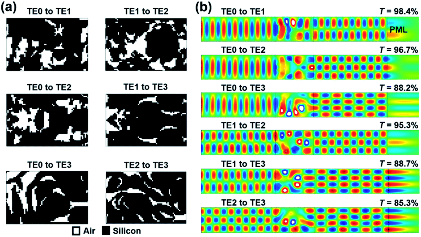
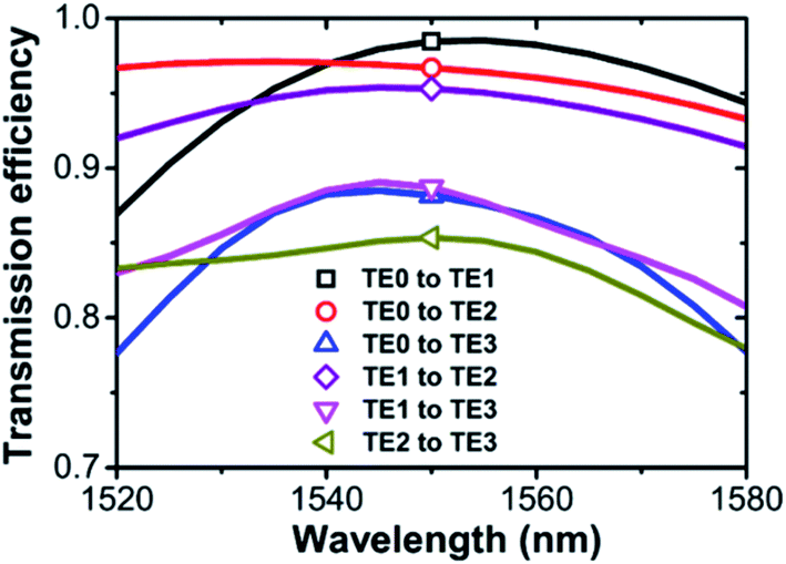
The adopted 1 μm-width silicon waveguide supports four TE modes. Compared with TE0 to TE1 mode conversion shown above, the precise conversion between specific modes is a more complicated task but desirable as well. Since only linear materials (silicon and air) are considered, the functional region is a linear device following time-reversal symmetry. In this sense, we need to explore six digital metamaterials for all possible conversions between these four modes. The proposed topology optimization method is easily extended to this task without modification, but only with a new objective function for the targeted mode. The obtained digital metamaterials for mode conversions, including TE0 to TE1, TE0 to TE2, TE0 to TE3, TE1 to TE2, TE1 to TE3 and TE2 to TE3, are plotted in Fig. 3(a). To demonstrate the functionality, we plot the simulated magnetic fields at center wavelength in Fig. 3(b) and the corresponding transmission efficiencies are also listed. For conversions to TE1 and TE2, the transmission efficiencies are higher than 95%, while for conversions to TE3, the values are in the range between 85% and 89%. This decrease does not come from the insertion of digital metamaterials, but the less confinement of TE3. As shown in Fig. 4, the transmission spectra within a 60 nm operational bandwidth indicate that these topologically designed digital metamaterials are broadband high-quality mode converters. The performances presented are comparable with those of the designs in ref. 25 while the binary design in our work consists of only air and silicon pixels. The amounts of air and silicon pixels inside the proposed functional regions are listed in Table S1.† Moreover, one should note the influence of pixel size on the topology design of a photonic device. Larger pixel size inside the digital metamaterials can reduce the challenges for experimental fabrication, but decrease the design freedom which may sacrifice the performance and even lead to failure to find a design for such complicated mode manipulation. Since we aim to achieve high performance in the functional region with footprint (in length) below 1550 nm and keep the number of pixels to an integer, a 25 nm pixel size is chosen. This value is comparable with the design units with length λ/40 in ref. 25 and 26. As a comparison, TE0-to-TE1 and TE0-to-TE2 mode converters are redesigned with 50 nm pixel size, as shown in Fig. S1.† It can be seen that both transmission efficiency and mode purity are slightly lower, but still acceptable.
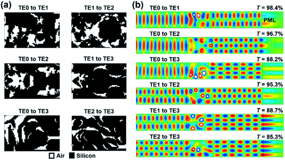 |
| | Fig. 3 (a) Digital metamaterials for six mode conversions. (b) Magnetic fields of six mode converters simulated at center wavelength. | |
 |
| | Fig. 4 Transmission spectra of six mode converters. | |
3.2 Reciprocal unidirectional transmission
The unidirectional transmission of light in a silicon waveguide has attracted huge interest in the last decade, especially the schemes based on linear and passive integrated devices.2,8–10,26 Due to the linear regime, time-reversal symmetry is held. Such devices are naturally not optical isolators but optical diodes for specific modes. The underlying mechanism is simply asymmetric mode conversion which relies on the precise control of mode order or polarization. Based on the obtained mode order conversion results, the digital metamaterial for optical diodes can be further pursued. We only focus on the unidirectional transmission of the TE0 mode as an exemplary case. In this scheme, the TE0 mode is expected to be converted to the TE1 mode in the forward direction, while in the backward direction, the TE0 mode will be forbidden to transmit through the functional region. Therefore, we start with the TE0-to-TE1 design shown in Fig. 2(a). The forward conversion is already achieved and needs to be kept. The only modification is an additional term in the new objective function which can be expressed as| |  | (3) |
The integral of backward power flux is simpler because we only need to eliminate the light in this direction.
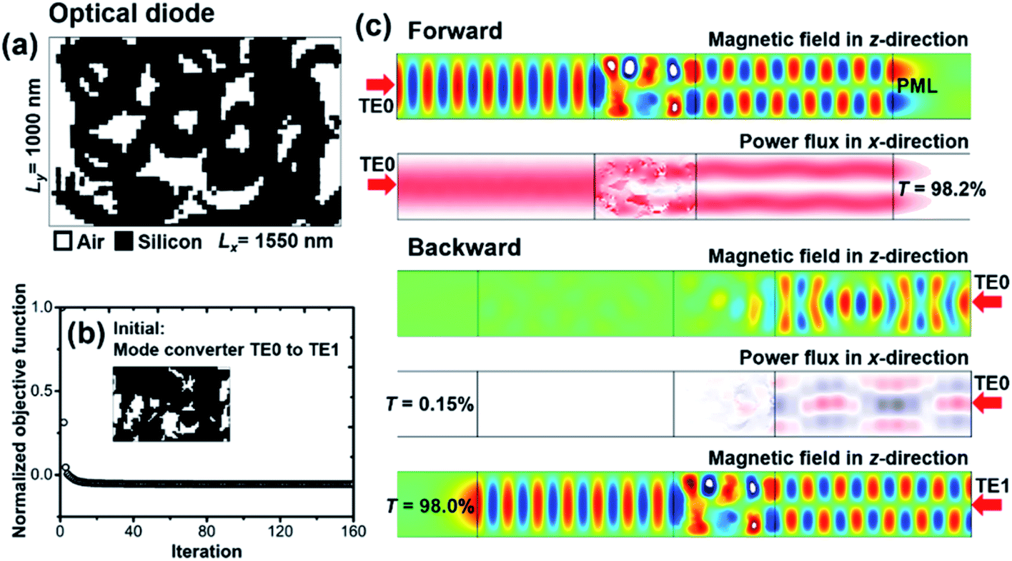
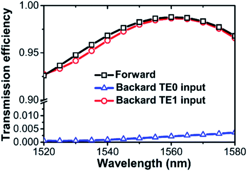
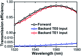
The topologically designed digital metamaterial for unidirectional transmission of TE0 is shown in Fig. 5(a). Starting from the mode converter, the optimization uses about 160 iterations to be converged to an optical diode. Again, the MMA algorithm shows high efficiency by the rapid decrease of the objective function in the initial stage. With the TE0 mode imported from left and right port, the magnetic field (z-direction) and power flux (x-direction) simulated at center wavelength of 1550 nm are plotted in Fig. 5(c). As expected, TE0 is converted to TE1 in forward direction with transmission efficiency Tf = 98.2%, while this value for TE0 in backward direction is only Tb = 0.15%. The contrast ratio, defined as rc = (Tf − Tb)/(Tf + Tb), reaches 0.997. When considering the unidirectionality defined as U = 10![[thin space (1/6-em)]](https://www.rsc.org/images/entities/char_2009.gif) log10(Tf/Tb), the peak value is approximately 28 dB, which is higher than that of our previous designs based on photonic crystals12,13 and surface plasmonics.8 If TE1 is excited at the right-hand port, TE1 is converted back to TE0 in the backward direction. It can be seen that the magnetic fields are nearly identical between the uppermost and lowermost plots in Fig. 5(c), confirming the time-reversal symmetry in this reciprocal optical diode. As shown in Fig. 6, the forward transmission efficiency keeps higher than 92.6% from 1520 nm to 1580 nm, while the value keeps lower than 0.37% in the backward direction. The minimum contrast ratio is 0.992 (24 dB unidirectionality) within the 60 nm operational bandwidth.
log10(Tf/Tb), the peak value is approximately 28 dB, which is higher than that of our previous designs based on photonic crystals12,13 and surface plasmonics.8 If TE1 is excited at the right-hand port, TE1 is converted back to TE0 in the backward direction. It can be seen that the magnetic fields are nearly identical between the uppermost and lowermost plots in Fig. 5(c), confirming the time-reversal symmetry in this reciprocal optical diode. As shown in Fig. 6, the forward transmission efficiency keeps higher than 92.6% from 1520 nm to 1580 nm, while the value keeps lower than 0.37% in the backward direction. The minimum contrast ratio is 0.992 (24 dB unidirectionality) within the 60 nm operational bandwidth.
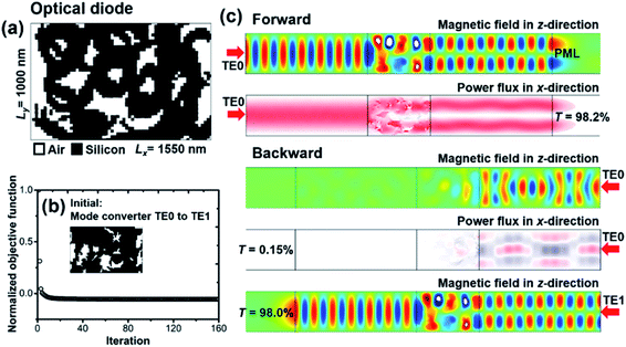 |
| | Fig. 5 (a) Digital metamaterial for optical diode. (b) Optimization convergence diagram of optical diode starting from TE0-to-TE1 mode converter. (c) Forward and backward magnetic fields and power fluxes simulated at center wavelength. | |
 |
| | Fig. 6 Forward and backward transmission spectra of optical diode. | |
3.3 Mode division multiplexing
Besides reciprocal unidirectional transmission, mode division multiplexing (MDM) is another promising application of precise mode order manipulation, which enhances the transmission capacity of on-chip optical interconnection from an additional dimension to the wavelength.19,21,32,39 Each mode inside the bus waveguide carries information individually, even at identical wavelength. Here, we focus on topologically designing a compact 1 × 2 demultiplexer. As shown in Fig. 7, the footprint of the demultiplexer is set as small as 1.55 μm × 1.55 μm (1.0λ2) and divided to 63 × 63 pixels. The size of each pixel is the same as described in previous sections. The multimode bus waveguide is set at 1 μm in width to support at least two modes, and the two output waveguides, with Port A and Port B, are set at 0.4 μm in width. The demultiplexer routes a certain mode to a certain output waveguide, based on which the objective function is built and can be expressed as| |  | (4) |
 |
| | Fig. 7 (a) Digital metamaterial for 1 × 2 demultiplexer. (b) Optimization convergence diagram of demultiplexer. (c) Magnetic fields and power fluxes simulated at center wavelength with TE0 and TE1 modes imported in bus waveguide. | |
To avoid the impact of an initial guess, the topology optimization starts with the simplest configuration, namely a pure silicon region without air.
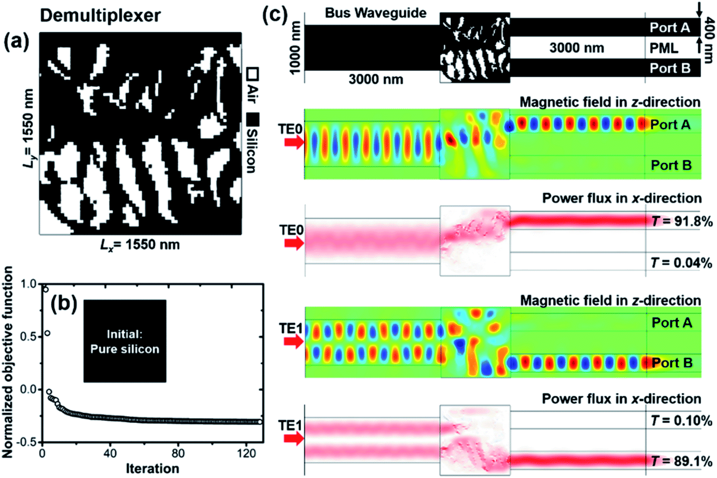
The digital metamaterial obtained for the demultiplexer is plotted in Fig. 7(a). Starting from pure silicon, it takes the optimization process about 130 iterations to converge to a demultiplexer. Since the objective function is quite different and more complicated, the general applicability of the adopted method combing FEM, DM and MMA is well demonstrated. As shown by the magnetic field and power flux distributions in Fig. 7(c), when the TE0 mode is transmitted in the bus waveguide, the light is routed to the upper waveguide. The transmission efficiencies measured at Port A and Port B are 91.8% and 0.04%, respectively. On the contrary, when the TE1 mode is transmitted in the bus waveguide, the light is routed to the lower waveguide. The transmission efficiencies are 0.10% and 89.1% for Port A and Port B, respectively. These FEM simulations are performed at center wavelength of 1550 nm. The corresponding contrast ratios are respectively 0.999 and 0.998, indicating the satisfactory performance of this demultiplexer.
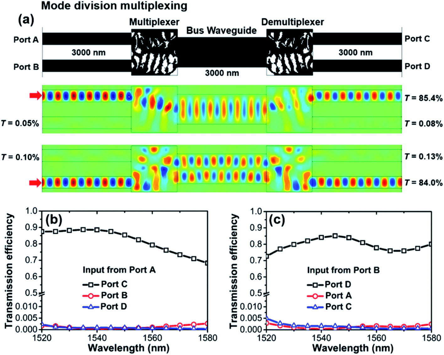
To further demonstrate the functionality and evaluate the performance, it behooves us to build an MDM system. As shown in Fig. 8(a), from left to right, the MDM system is composed of two input waveguides, a multiplexer, a bus waveguide, a demultiplexer and two output waveguides. Since the digital metamaterial consists of only linear silicon and air, the multiplexer can be obtained by simply mirroring the design of the demultiplexer due to the reciprocal feature. In this scheme, the upper waveguides (Port A and Port C) form a channel, while the other two (Port B and Port D) form another channel. TE0 and TE1 modes in the bus waveguide are individually utilized as the carriers for these two channels. The magnetic fields simulated at the center wavelength of 1550 nm are plotted in Fig. 8(a). If light is imported from Port A and passes the multiplexer, the TE0 mode is excited and transmits in the bus waveguide, and then the demultiplexer routes the light to Port C. The transmission efficiencies measured at Port C, Port B and Port D are 85.4%, 0.05% and 0.08%, respectively. When we consider the other channel carried by the TE1 mode, the transmission efficiencies measured at Port D, Port A and Port C are 84.0%, 0.13% and 0.10%, respectively. The contrast ratio accounting for channel crosstalk is 0.998 for the TE0 channel and 0.997 for the TE1 channel, reflecting a good performance of the MDM system. Within a 60 nm operational bandwidth, the transmission spectra measured at the ports are plotted in Fig. 8(b) and (c) for TE0 and TE1 channels, respectively. No obvious degradation is observed.
 |
| | Fig. 8 (a) Schematic of an MDM system and corresponding magnetic fields simulated at center wavelength. (b) Transmission spectra with input from Port A. (c) Transmission spectra with input from Port B. | |
3.4 Quasi-3D designs
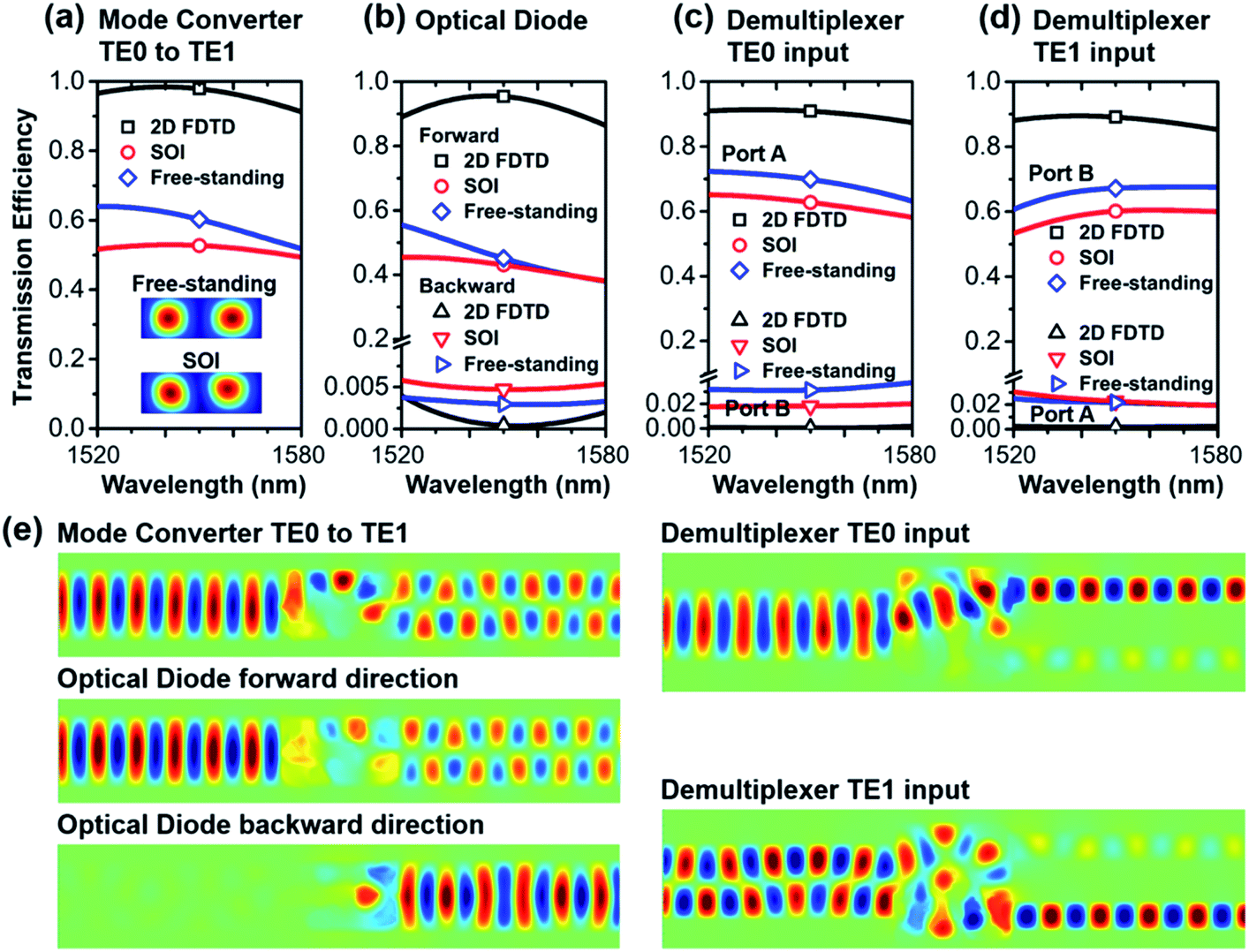
The proposed topology optimization method combining DM and MMA needs to run with 2D FEM simulation at the moment. In previous sections, the refractive index of silicon is set at n = 3.464, which corresponds to infinite thickness of the slab waveguide. When the thickness of the waveguide reduces, a blue shift of the transmission spectrum is expected due to the reduction of effective refractive index. To maintain the same operational wavelength range (1520 nm to 1560 nm) for a real device integrated with a 340 nm thick silicon slab waveguide,11,30 the refractive index of silicon in 2D FEM simulation (denoted as quasi-3D) has to be reduced to an equivalent value n = 3.0, determined by a tedious trial-and-error approach. We re-perform the topology optimizations for TE0-to-TE1 mode converter, optical diode and demultiplexer with exactly same strategies. The newly obtained quasi-3D designs are plotted in Fig. 9(a). Despite the silicon and air patterns being different from those of previous sections due to the change of refractive index of silicon, the major performances remain similar, as shown in Fig. 9(b) and (c).
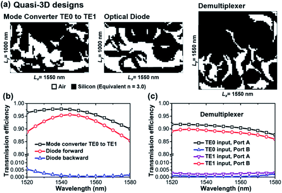 |
| | Fig. 9 (a) Digital metamaterials of quasi-3D designs. (b) Transmission spectra of mode converter and optical diode. (c) Transmission spectra of demultiplexer with TE0 and TE1 modes as input. | |
In experiments, E-beam lithography and reactive ion etching are needed to fabricate such inversely designed digital metamaterials whose length of pixels is at the nanometer scale. Major error may occur in both material and shape of these square pixels. Instead of square, a circular shape of air hole is introduced to avoid the edge distortion in some recent designs.34,35 Unfortunately, this treatment only suits the inverse design strategy for predefined pixels and is not compatible with the adopted DM in which the distribution of dielectric material is described by a single design variable. In this sense, we assume the shape of a pixel is perfect and focus on the wrong material for the pixel as the fabrication error. To account for this kind of error, pixels with wrong material are randomly introduced to the quasi-3D designs for optical diode and demultiplexer. The relation between performances and the error percentage are demonstrated in Figs. S2 and S3.† Eight diode samples and five demultiplexer samples are simulated for each error percentage from 2% to 5%. As can be seen, 3% error can be acceptable for both devices, indicating the robustness of the proposed designs.
Finally, a 3D FDTD simulation is performed to validate the functionalities and performances of the quasi-3D designs. The thickness of waveguide and digital metamaterials is set at 340 nm.11,30 Two cases are considered: free-standing models and models sitting on top of a SiO2 layer without cladding layer (denoted as SOI). The sizes of monitors used to collect the output light are set exactly the same as the waveguide cross-section. Additionally, we give a test for 2D FDTD simulations with n = 3.0 first. Consistent results with 2D FEM simulations are obtained if comparing the transmission spectra plotted in Fig. 9 and 10. For 3D TE0-to-TE1 mode converter, the transmission efficiencies remain higher than 49% for both free-standing and SOI cases, while the values at center wavelength are 60.3% and 52.7%, respectively. As shown in the inset of Fig. 10(a), the output power flux at 1550 nm has two clear and separated peaks, indicating acceptable quality of the conversion to the TE1 mode. For the optical diode, the contrast ratios between forward and backward directions respectively keep higher than 0.983 (20.6 dB unidirectionality) and 0.972 (18.4 dB unidirectionality) for free-standing and SOI cases, which are higher than for previously reported pixelated inverse designs.26,32 As shown by the spectra plotted in Fig. 10(c) and (d), the demultiplexer clearly routes the power of the TE0 mode and TE1 mode to Port A and Port B, respectively. The contrast ratios between the two output ports keep higher than 0.9 within the 60 nm operational bandwidth for all cases. Generally, the performances of free-standing models are slightly better than those of SOI models. Detailed comparisons between the proposed mode converter, optical diode and demultiplexer with reported designs are listed in Tables S2–S5.† Moreover, the magnetic fields measured on the center cross-section of 3D models are nearly identical to those from 2D simulations at the same wavelength, providing a validation of such quasi-3D design strategy. However, 3D FDTD results are still facing degradation. The links between 2D optimization and 3D simulation still need to be further investigated.
 |
| | Fig. 10 Transmission spectra from 2D and 3D FDTD simulations (free-standing and SOI). (a) TE0-to-TE1 mode converter. (b) Optical diode. (c) Demultiplexer with TE0 mode input. (d) Demultiplexer with TE1 mode input. (e) Magnetic fields observed on the center cross-section of 3D models. | |
4. Conclusions
In summary, we proposed ultra-compact designs for mode order manipulation in a silicon waveguide based on digital metamaterials consisting of silicon and air pixels. All functional regions obtained by topologically designing are below square of center wavelength in terms of footprint. Six mode order conversions between TE0, TE1, TE2 and TE3 in a 1 μm-width waveguide with high efficiency and high mode purity are firstly demonstrated. Based on the forward TE0-to-TE1 mode conversion, a reciprocal optical diode is further obtained by adding an additional objective in optimization to block the TE0 mode in backward direction. Moreover, with the same method, we design a 1 × 2 demultiplexer for TE0 and TE1 modes in a bus waveguide, and demonstrate a simple MDM system with satisfactory performances. Finally, the functionalities are validated by 3D FDTD simulations. We expect that the proposed waveguide-integrated digital metamaterials for mode order manipulation can play important roles in on-chip all-optical interconnections.
Author contributions
HY – conceptualization, methodology, formal analysis, funding acquisition, writing – original draft; YW – formal analysis; SZ – writing – review and editing; DW – writing – review and editing; YL – writing – review and editing; MW – conceptualization, writing – review and editing; QZ – funding acquisition, writing – review and editing.
Conflicts of interest
There are no conflicts to declare.
Acknowledgements
The financial support of this work is from the National Natural Science Foundation of China (no. 61975123, 61671090) and Fund of State Key Laboratory of Information Photonics and Optical Communications (Beijing University of Posts and Telecommunications), PR China (IPOC2020ZT01).
References
- D. Jalas, A. Petrov, M. Eich, W. Freude, S. Fan, Z. Yu, R. Baets, M. Popović, A. Melloni, J. D. Joannopoulos, M. Vanwolleghem, C. R. Doerr and H. Renner, What is - and what is not - an optical isolator, Nat. Photonics, 2013, 7, 579 CrossRef CAS.
- V. Liu, D. A. B. Miller and S. Fan, Ultra-compact photonic crystal waveguide spatial mode converter and its connection to the optical diode effect, Opt. Express, 2012, 20, 28388 CrossRef PubMed.
- L. Luo, N. Ophir, C. P. Chen, L. H. Gabrielli, C. B. Poitras, K. Bergmen and M. Lipson, WDM-compatible mode-division multiplexing on a silicon chip, Nat. Commun., 2014, 5, 3069 CrossRef PubMed.
- D. Dai, J. Wang and Y. Shi, Silicon mode (de)multiplexer enabling high capacity photonic networks-on-chip with a single-wavelength-carrier light, Opt. Lett., 2013, 38, 1422 CrossRef CAS PubMed.
- D. Garcia-Rodriguez, J. L. Corral, A. Griol and R. Llorente, Dimensional variation tolerant modeconverter/multiplexer fabricated in SOI technology for two-mode transmission at 1550 nm, Opt. Lett., 2017, 42, 1221 CrossRef CAS PubMed.
- B. B. Oner, K. Ustun, H. Kurt, A. K. Okyay and G. Turhan-Sayan, Large bandwidth mode order converter by differential waveguides, Opt. Express, 2015, 23, 3186 CrossRef CAS PubMed.
- B. T. Lee and S. Y. Shin, Mode-order converter in a multimode waveguide, Opt. Lett., 2003, 28, 1660 CrossRef.
- J. Li, H. Ye, Z. Yu and Y. Liu, Design of a broadband reciprocal optical diode in a silicon waveguide assisted by silver surface plasmonic splitter, Opt. Express, 2017, 25, 19129 CrossRef CAS PubMed.
- C. Wang, C. Z. Zhou and Z. Y. Li, On-chip optical diode based on silicon photonic crystal heterojunctions, Opt. Express, 2011, 19, 26948 CrossRef CAS PubMed.
- S. Feng and Y. Wang, Unidirectional reciprocal wavelength filters based on the square-lattice photonic crystal structures with the rectangular defects, Opt. Express, 2013, 21, 220 CrossRef PubMed.
- L. H. Frandsen, Y. Elesin, L. F. Frellsen, M. Mitrovic, Y. Ding, O. Sigmund and K. Yvind, Topology optimized mode conversion in a photonic crystal waveguide fabricated in silicon-on insulator material, Opt. Express, 2014, 22, 8525 CrossRef CAS PubMed.
- H. Ye, Z. Yu, Y. Liu and Z. Chen, Realization of compact broadband optical diode in linear air-hole photonic crystal waveguide, Opt. Express, 2016, 24, 24592 CrossRef.
- H. Ye, D. Wang, Z. Yu, J. Zhang and Z. Chen, Ultra-compact broadband mode converter and optical diode based on linear rod-type photonic crystal waveguide, Opt. Express, 2015, 23, 9673 CrossRef CAS PubMed.
- Z. Y. Li, M. H. Kim, C. Wang, Z. H. Han, S. Shrestha, A. C. Overvig, M. Lu, A. Stein, A. M. Agarwal, M. Lončar and N. F. Yu, Controlling propagation and coupling of waveguide modes using phase-gradient metasurfaces, Nat. Nanotechnol., 2017, 12, 675 CrossRef CAS PubMed.
- D. Chen, X. Xiao, L. Wang, Y. Yu, W. Liu and Q. Yang, Low-loss and fabrication tolerant silicon mode order converters based on novel compact tapers, Opt. Express, 2015, 23, 11152 CrossRef CAS PubMed.
- D. Ohana, D. Boris, N. Mazurski and U. Levy, Dielectric metasurface as a platform for spatial mode conversion in nanoscale waveguides, Nano Lett., 2016, 16, 7956 CrossRef CAS.
- D. Ohana and U. Levy, Mode conversion based on dielectric metamaterial in silicon, Opt. Express, 2014, 22, 27617 CrossRef CAS PubMed.
- D. Zhu, J. Zhang, H. Ye, Z. Yu and Y. Liu, Design of a broadband reciprocal optical diode in multimode silicon waveguide by partial depth etching, Opt. Commun., 2018, 418, 88 CrossRef CAS.
- W. Jiang, J. Miao and T. Li, Compact silicon 10-mode multi/demultiplexer for hybrid mode- and polarisation-division multiplexing system, Sci. Rep., 2019, 9, 13223 CrossRef PubMed.
- Z. Cheng, J. Wang, Z. Yang, L. Zhu, Y. Yang, Y. Huang and X. Ren, Sub-wavelength grating assisted mode order converter on the SOI substrate, Opt. Express, 2019, 27, 34434 CrossRef CAS PubMed.
- Y. He, Y. Zhang, Q. Zhu, S. An, R. Cao, X. Guo, C. Qiu and Y. Su, Silicon High-Order Mode (De)Multiplexer on Single Polarization, J. Lightwave Technol., 2018, 36, 5746 CAS.
- S. Molesky, Z. Lin, A. Y. Piggott, W. Jin, J. Vucković and A. W. Rodriguez, Inverse design in nanophotonics, Nat. Photonics, 2018, 12, 659 CrossRef CAS.
- K. Aydin, Nanostructured silicon success, Nat. Photonics, 2015, 9, 353 CrossRef CAS.
- A. Y. Piggot, J. Lu, K. G. Lagoudakis, J. Petykiewicz, T. M. Babinec and J. Vuckovic, Inverse design and demonstration of a compact and broadband on-chip wavelength demultiplexer, Nat. Photonics, 2015, 9, 347 CrossRef.
- J. Lu and J. Vuckovic, Objective-first design of high-efficiency, small-footprint couplers between arbitrary nanophotonic waveguide modes, Opt. Express, 2012, 20, 7221 CrossRef PubMed.
- F. Callewaert, S. Butun, Z. Li and K. Aydin, Inverse design of an ultra-compact broadband optical diode based on asymmetric spatial mode conversion, Sci. Rep., 2016, 6, 32577 CrossRef CAS PubMed.
- K. Svanberg, The method of moving asymptotes-a new method for structural optimization, Int. J. Numer. Methods Eng., 1987, 24, 359 CrossRef.
- B. Shen, P. Wang, R. Polson and R. Menon, An integrated-nanophotonics polarization beamsplitter with 2.4 × 2.4 μm2 footprint, Nat. Photonics, 2015, 9, 378 CrossRef CAS.
- Q. Lu, X. Yan, W. Wei, X. Zhang, M. Zhang, J. Zheng, B. Li, Y. Luo, Q. Lin and X. Ren, High-speed ultra-compact all-optical NOT and AND logic gates designed by a multi-objective particle swarm optimized method, Opt. Laser Technol., 2019, 116, 322 CrossRef CAS.
- L. F. Frellsen, Y. Ding, O. Sigmund and L. H. Frandsen, Topology optimized mode multiplexing in silicon-on-insulator photonic wire waveguides, Opt. Express, 2016, 24, 16866 CrossRef CAS.
- H. Jia, S. L. Yang, T. Zhou, L. Zhang, T. Wang, H. X. Chen, J. H. Yang and L. Yang, Mode-Oriented Permutation Cipher Encryption and Passive Signal Switching Based on Multiobjective Optimized Silicon Subwavelength Metastructures, ACS Photonics, 2020, 7, 2163 CrossRef CAS.
- B. Shen, R. Polson and R. Menon, Integrated digital metamaterials enables ultra-compact optical diodes, Opt. Express, 2015, 23, 10847 CrossRef CAS PubMed.
- M. H. Tahersima, K. Kojima, T. Koike-Akino, D. Jha, B. N. Wang, C. W. Lin and K. Parsons, Deep Neural Network Inverse Design of Integrated Photonic Power Splitters, Sci. Rep., 2019, 9, 1368 CrossRef.
- H. Xie, Y. Liu, S. Wang, Y. Wang, Y. Yao, Q. Song, J. Du, Z. He and K. Xu, Highly Compact and Efficient Four-Mode Multiplexer Based on Pixelated Waveguides, IEEE Photonics Technol. Lett., 2020, 32, 166 CAS.
- W. Chang, L. Lu, X. Ren, L. Lu, M. Cheng, D. Liu and M. Zhang, An Ultracompact Multimode Waveguide Crossing Based on Subwavelength Asymmetric Y-Junction, IEEE Photonics J., 2018, 10, 4501008 Search PubMed.
- M. P. Bendsøe, Optimal shape design as a material distribution problem, Structural Optimization, 1989, 1, 193 CrossRef.
- F. Wang, B. S. Lazarov and O. Sigmund, On projection methods, convergence and robust formulations in topology optimization, Struct. Multidiscip. O., 2011, 43, 767 CrossRef.
- K. Svanberg, A class of globally convergent optimization methods based on conservative convex separable approximations, Siam J. Optimiz., 2002, 12, 555 CrossRef.
- Y. He, Y. Zhang, H. Wang, L. Sun and Y. Su, Design and experimental demonstration of a silicon multi-dimensional (de)multiplexer for wavelength-, mode- and polarization-division (de)multiplexing, Opt. Lett., 2020, 45, 2846 CrossRef PubMed.
Footnote |
| † Electronic supplementary information (ESI) available. See DOI: 10.1039/d1na00198a |
|
| This journal is © The Royal Society of Chemistry 2021 |
Click here to see how this site uses Cookies. View our privacy policy here. 
 Open Access Article
 This Open Access Article is licensed under a Creative Commons Attribution-Non Commercial 3.0 Unported Licence
 *a,
Yanrong
Wang
a,
Shuhe
Zhang
a,
Danshi
Wang
a,
Yumin
Liu
*a,
Yanrong
Wang
a,
Shuhe
Zhang
a,
Danshi
Wang
a,
Yumin
Liu