
 Open Access Article
 This Open Access Article is licensed under a Creative Commons Attribution-Non Commercial 3.0 Unported Licence
Dynamics of the charging-induced imaging instability in transmission electron microscopy†
Linhai
Wang
a,
Dongdong
Liu
a,
Fan
Zhang
b,
Zhenyu
Zhang
 *a,
Junfeng
Cui
a,
Zhenghao
Jia
b,
Zhibin
Yu
a,
Yiqiang
Lv
a and
Wei
Liu
*b
*a,
Junfeng
Cui
a,
Zhenghao
Jia
b,
Zhibin
Yu
a,
Yiqiang
Lv
a and
Wei
Liu
*b
aKey Laboratory for Precision and Non-Traditional Machining Technology of Ministry of Education, Dalian University of Technology, Dalian 116024, China. E-mail: zzy@dlut.edu.cn
bDivision of Energy Research Resources, Dalian National Laboratory for Clean Energy, Dalian Institute of Chemical Physics, Chinese Academy of Sciences, Dalian 116023, China. E-mail: weiliu@dicp.ac.cn
First published on 4th March 2021
Abstract
Revolutionary microscopy technologies for aberration correction in spatial and energy aspects have exhibited continuous progress, pushing forward the information limit of materials research down to a scale of sub-angstrom and milli-electron voltage. Nevertheless, imaging quality could still suffer due to sample instability, e.g. the charging effect, which always comes along with electron microscopy characterizations. Herein, using a defocus estimation algorithm and an in situ image feature tracking method, we quantitatively studied the image drifting dynamics induced by the charging on transmission electron microscopy (TEM) carrier grids with tunable electrical conductivity. Experimental evidence clarifies the debate about the charge types, proving that the irradiation of the electron beam induces a positive charge on the grid sample of poor electrical conductivity. Such charge accumulation accounts for subsequent imaging instability, including the increase of defocus and the drift of lateral images. Particularly, the competition between charging and discharging was found to dynamically modulate the propagation of electron beam, resulting in a periodically reciprocating movement on TEM images. These findings enrich understanding on the dynamic principle of charging effects as well as the details of image drifting behaviors. It also suggests specific attention on the importance of conductivity control on a TEM specimen, beyond all the efforts for instrumental improvements.
Introduction
Higher resolution for more atomic structural information has been a long-standing pursuit of scanning/transmission electron microscopy (S/TEM); hence, microscopists devote themselves with tremendous efforts to overcome the instrumental defects from either the electron source quality or the electromagnetic lenses via developing correctors to reduce the influence of both spherical and temporal aberrations.1,2 Major breakthroughs in modern TEM realize the successful correction of up to fifth-order aberration, facilitating a spatial resolution down to the level of half-angstrom.3 However, merits from these revolutionary instrumental improvements could be quite difficult when applied to a practical TEM sample of poor electrical conductivity (e.g., semiconductors, metal oxides, silicates et al.), which could probably suffer from imaging instability issues due to the charging effects induced by the electron beam irradiation. Such charging-induced imaging instability could be a challenge out of tolerance particularly for those attempts of atomic structure imaging. Moreover, it also reports that the charging effects would not only induce imaging aberration and shifting but also cause damages and structural defects to the sample.4,5Rooted in the intrinsic interactions between the incident beam and materials for observation, a charging phenomenon is understood within the framework of electron capture and second electron (SE) excitation and emission procedures, which are described quite differently in previous studies in diverse scenarios of electron beam irradiation. First, from the perspective of electrostatic field (EF) formed by incident e-beam and excited SE, Cazaux J. theoretically analyzed the charging effects on an insulator surface by considering the SE emission yield;6,7 on the other hand, a dynamic double-layer model aiming to describe the temporal correlation of charge effects was proposed by Melchinger A. and S. Hofmann.8 Despite these efforts, debates remain unresolved for the charging types (positive or negative). S. Hettler, et al. report a thin carbon film being negatively charged at a moderate temperature,9 while other researchers believe that beam irradiation leads to a positive charge on a thin sample.10 Besides, previous work on the charging effect, which is thought usually but could yield serious interference to microscopy imaging. At present, researchers mainly focus on the theoretical studies of thick samples in SEM imaging,11,12 whereas experimental explorations on the quantitative dynamics of charging-induced instability in TEM imaging are rare. However, this turns out to be significant because an image stability issue becomes more critical in the aberration-corrected microscopy.
In this study, we present an experimental study on the dynamics of the charging-induced image drift under TEM conditions. The tunable electrical conductivity was realized on a commercial TEM grid in an innovative design of sandwich-like configuration giving the capability of changing charge transport resistances to verify the influence of charging effects during TEM imaging. We were able to precisely determine the charging-induced image shift either along the beam direction of Z axis or within the XY plane of the sample by developing algorithms dedicated to track the defocus change and image drift. The quantitative analysis on experimental results confirms that in TEM the beam irradiation positively charges a thin film sample because of distinct image drifting characteristics including the increase of defocus and lateral shift of images in the sample plane. A delicate reciprocating movement during the imaging drift was first discovered, which presents good agreement with the dynamic equilibrium driven by the periodic competition between charging and discharging procedures. In this study, the demonstration of the charging-induced imaging instability would arouse general attention of researchers on the quality control of sample conductivity that is vital for TEM characterization.
Results and discussion
To precisely evaluate the charging-induced imaging drift along the Z axis, the defocusing parameter is quantitatively calculated from the in situ recorded HRTEM series during sample charging under beam irradiation. In particular, the fast Fourier transform (FFT) patterns known as digital forms of Thon rings are produced from the acquired HRTEM images of an amorphous carbon film.13 Thon rings are composed of alternating light and dark rings with different radii, representing the luminance values (I) at different frequencies (μ). Experimental I–μ curves are also referred to power spectrum density (PSD).14–17 For each diffraction pattern, PSD was calculated by integrating the selected ring area, containing all light and dark rings conducted by ImageJ. The defocus values of the HRTEM image are contained in the contrast transfer function (CTF) fitted by the envelope function,18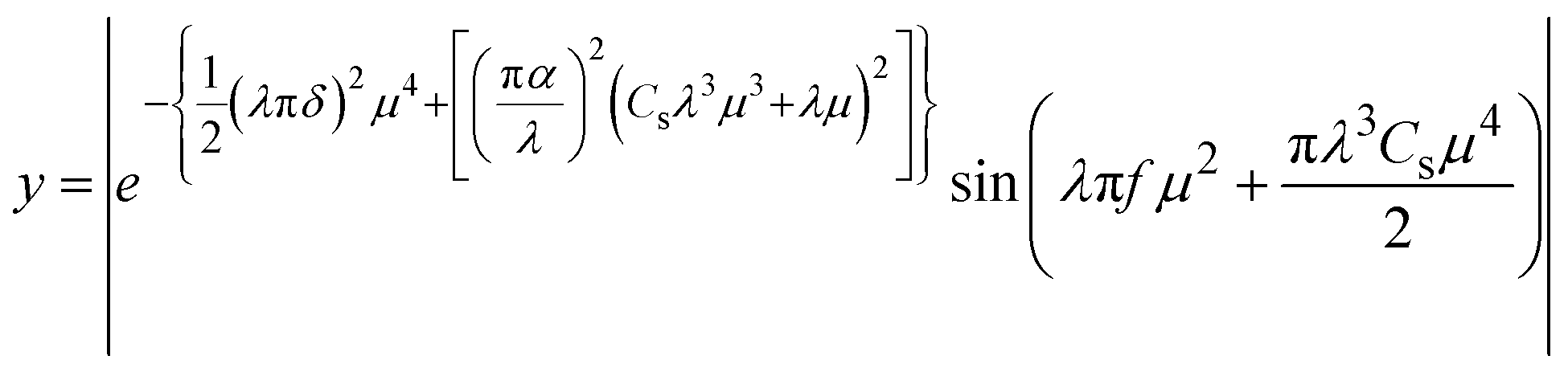 | (1) |
The PSD curves of samples and their corresponding fitted CTF ones as well as Thon rings are shown in Fig. 1. Fig. 1(a) illustrates the result of the gold (Au) grid with good electrical conductivity (sample I) before irradiation. It is measured to be 0.003 Ω and the defocus is calculated as −139.1 ± 1.6 nm; after being irradiated for 5 min (Fig. 1(b)), the defocus becomes −140.0 ± 1.5 nm, showing a small defocus variation of <1 nm that is almost negligible. While for sample II with an increased resistance of 1.065 Ω, the defocus increases from −416.3 ± 3.6 nm to −424.6 ± 2.7 nm after 5 min irradiation (Fig. 1(c and d)), which depicts that the focal length turns to increase by ∼8 nm at a moderate resistance. In order to obtain more significant imaging variation, sample III using the plastic underlay is studied, providing high resistance that is theoretically infinite. As shown in Fig. 1(e and f), before irradiation, the defocus of the image is calculated to be −108.1 ± 1.1 nm (Fig. 1(e)), while the defocus changes by a value of 57 nm after irradiation (Fig. 1(f)). Herein, it should be emphasized that all parameters for the irradiation treatments were kept identical in all three sample groups to drive the imaging defocus change. From the above-mentioned results, it is obvious that greater the resistance of the sample, the larger the increase in the image defocusing.
 | ||
| Fig. 1 PSDs (black dotted line) and their corresponding CTF curves (red line) of samples with different resistances for sample (I) low resistance (0.003 Ω), (a) before irradiation, (b) irradiated for 5 min, sample (II) moderate resistance (1.065 Ω), (c) before irradiation, (d) irradiated for 5 min, and sample (III) high resistance (insulator), (e) before irradiation, and (f) irradiated for 5 min. | ||
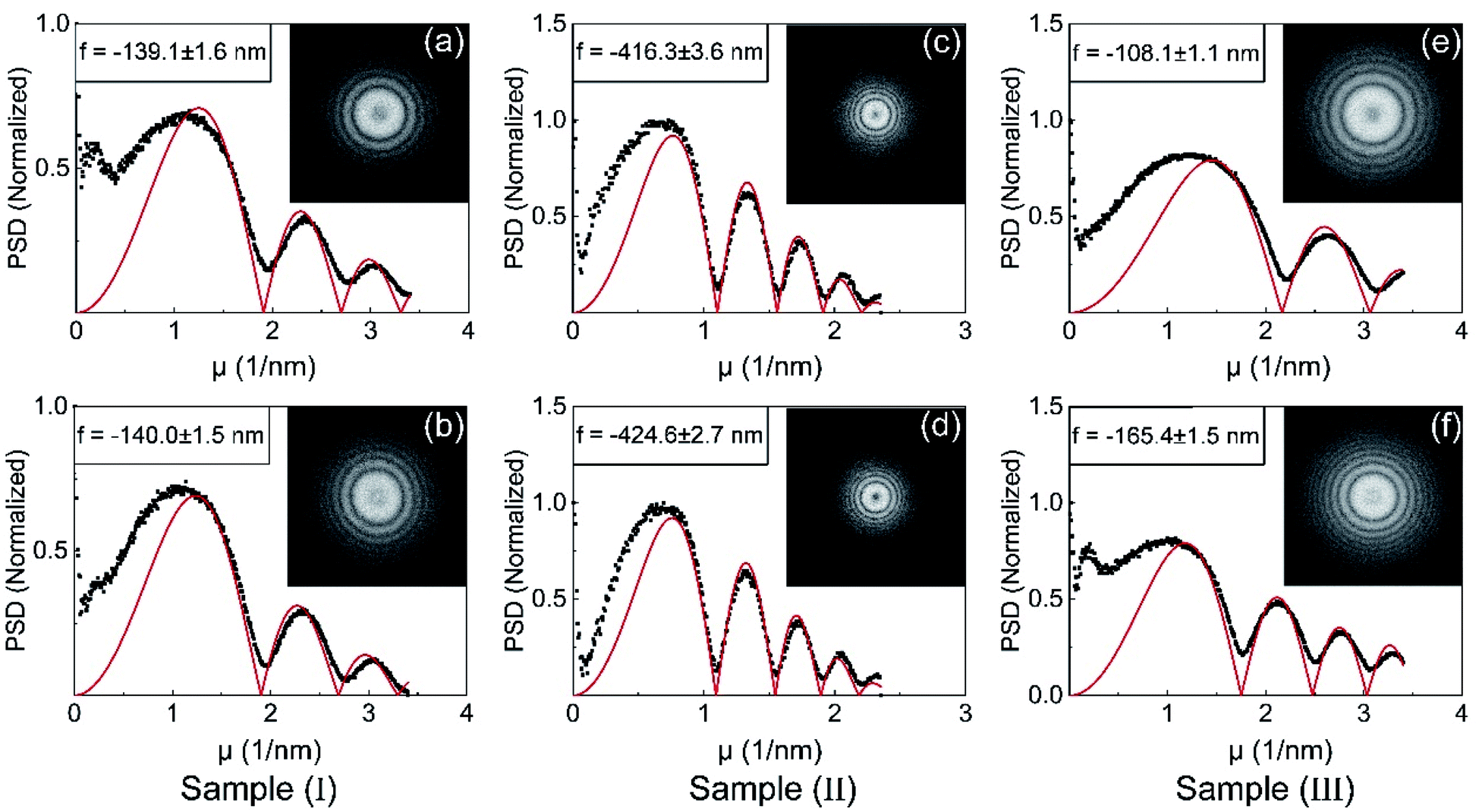
On the basis of the aforesaid exploration of the imaging drift behavior along the beam direction, the manner of image stability within the sample plane (horizontal drift) was investigated by tracking the movement trajectory of a sample feature in the real-time recorded image series (Fig. 2(a–c)). Fig. 2(d) demonstrates the horizontal displacement curve P(t) as a function of the beam irradiation time. It can be primarily divided into two movement manners at different periods: a monotonic movement, followed by a periodic oscillation around the final position. After the initial charging, the image moves along one direction (at −72.5° counterclockwise from the X axis) till the displacement of ∼20 nm within the first duration of 52 s. It is worth noticing that during a such one-way shifting procedure, the image simultaneously exhibits a periodic ‘fallback’ behavior. This turns out to be the dominant movement style at the next stage from 52 s to the end. A stable oscillation period of about 11–13 s is retained over the entire charging-induced imaging drift process, which has been unambiguously illustrated in Fig. 2(e)via plotting the drifting speed (first-order deviation of P(t)).
 | ||
| Fig. 2 Image shifting in the XY plane under high resistance for (a) the tracked particle in the OpenCV program at 0 s, (b) 52 s, (c) 90 s, (d) displacement–time function P(t) in the X direction, and (e) slope curve of function P(t). | ||
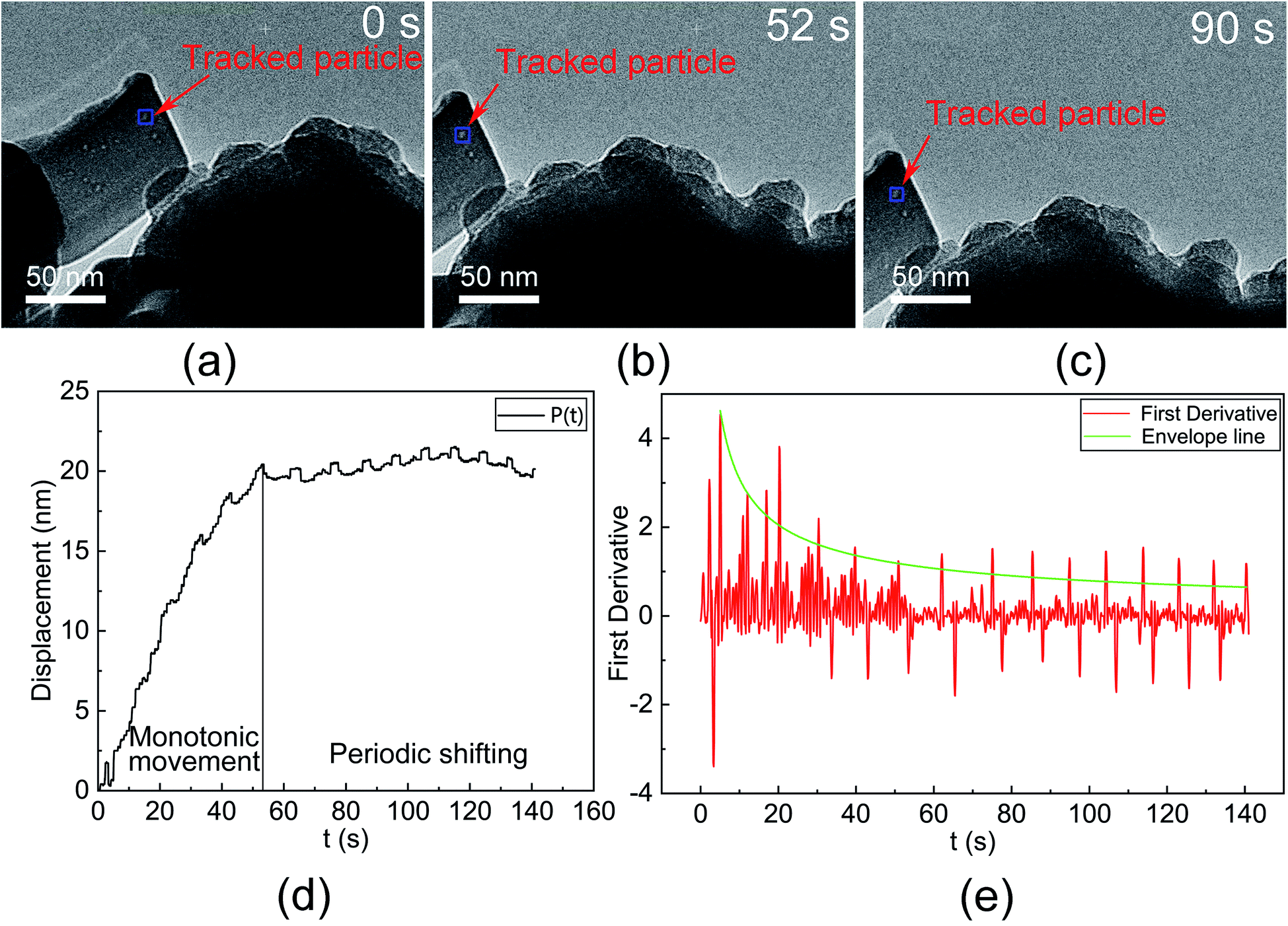
The irradiation by the electron beam can charge the TEM sample.1 Usually, charges derived from samples with a low resistance will be ground through holder in an instant causing no influence on the electron beam propagation, thus inducing no imaging instability issues. However, accompanied with the increase in the sample resistance, the mobility of flowing charge retarded causing charge accumulation on the sample, and therefore an EF is formed around the sample.8 Owing to such EF, some principle characteristics could be physically deduced. First, it is can be understood that EF is in asymmetry, which is ascribed to the asymmetric distribution of accumulated charges given the random contact between the TEM grid and the holder for every sample loading. Second, there always exists a discharging mechanism to compensate for the charging one as the grid is being continuously irradiated. Third, the asymmetric nature EF is expected to induce modulation on the electron wave propagation, vertically changing the beam focusing, while simultaneously horizontally shifting image position. Besides, to date, the charge type remains unclear, particularly under a TEM circumstance.
On the basis of experimental results through quantitative measurements, we were able to confirm the positive charging for the TEM thin film in this study for the first time. The mechanism details on the charging-induced imaging instability could also be discussed. Specifically, when an electron beam bombards a specimen, secondary and Auger electrons are stimulated from a thin surface layer, causing the asymmetry of charge distribution on the upper and lower surfaces of the sample (Z axis).14 On the other hand, within the sample plane, the electrons lost in the illumination area will be compensated from the surroundings for samples with good conductivity. However, for samples with a charge transport problem, charges accumulate near transition locations with resistances from low to high, such as the interfaces from sample to the supporting film, supporting film to the metal grid, and grid to the TEM holder. It is the random distribution at those transition sites that leads to the asymmetric charging and corresponding EFs both vertically and horizontally (Fig. 3(a)).
 | ||
| Fig. 3 Schematic diagrams of (a) charge distribution, (b) electronic deflection, and electron beam scattering (c) without vertical EF (before beam irradiation) and (d) with EF under irradiation. | ||
The consistent evidence of defocus increase for all the beam irradiated samples suggests that the beam electrons accelerate to a higher velocity as they pass through the sample, resulting in an extended focal length under the constant focusing strength of the objective lens. It is therefore an overall downward EF proves to exist owing to the asymmetric charge distribution on the upper and lower surfaces of the sample film. The schematic optical diagram for the charging-induced defocusing variation is displayed in Fig. 3(c and d), confirming that TEM samples are positively charged under irradiation. Due to the impact of vertical EF, the speed of electron beam incidence increases to V0 + ΔV, resulting in a reduced scattering angle α′ (red path) at the exit wave plane of the TEM sample, as shown in Fig. 3(d). In that case, the focal plane moves down to the focal plane, lowering the image plane to image plane′ and causing the enlargement of defocus.
The asymmetric charge distribution in the XY plane induces a lateral EF perpendicular to the beam propagation direction, accounting for the horizontal imaging drift drawn in Figs. 2(a–c). In the early stage of overall discharging from 0 to 52 s, the beam is deflected continuously by horizontal EF towards one direction, enabling the observed one-way drifting of the TEM image (Fig. 2(d)). Moreover, at some sites of the grid with charge accumulation, the continuous beam irradiation during imaging brings charge density to a critical threshold, where a maximal EF leads to the breakdown at that site and triggers localized discharging. A second charging cycle follows as the charge density stays below the threshold till the site reaches next the discharging point. The above oscillating behavior of localized charges is attributed to the intrinsic dynamics driving the TEM image to move shifts forward and backward, when the overall image displacement comes to the stable status from 52 s to the end revealed by Fig. 2(c and d).
Fig. 3(b) presents a simplified physical model of interaction between beam electron and horizontal EF without considering the spiral propagation. The EF E(t) is calculated,
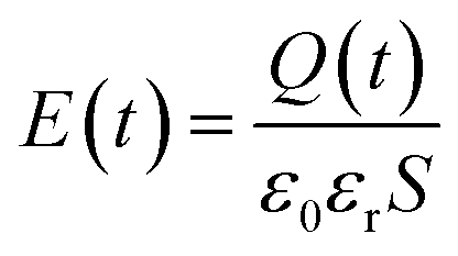 | (2) |
| F(t) = q0E(t) = m0a(t) | (3) |
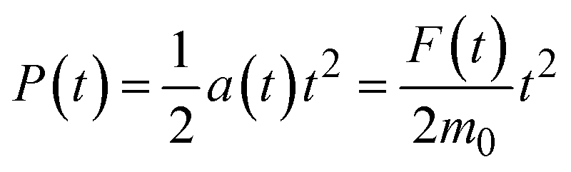 | (4) |
Substituting eqn (2) and (3) into eqn (4), it recasts,
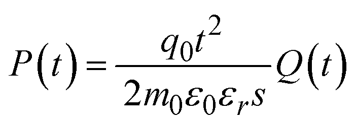 | (5) |
Differentiating on both sides, the drift velocity of the electron beam, equally for image drift, v(t) is,
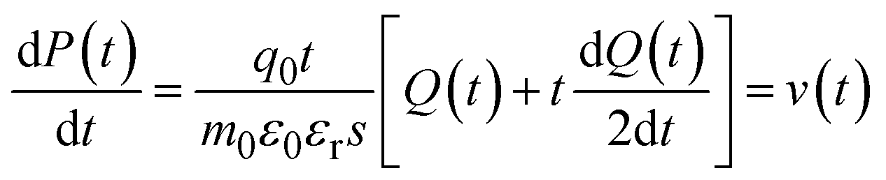 | (6) |
The drifting speed is influenced by the temporal term 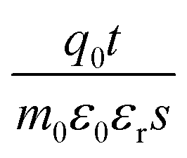 and charge accumulation term
 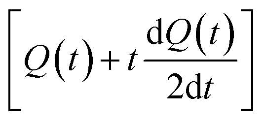 , in which the later one has primary determination on the variation of v(t) since it integrates the contribution of both Q(t) and t. Therefore, for the overall discharging process within the stage of beginning 52 s, the image drifting rate v(t) decreases quickly (Fig. 2(e)) as the Q(t) reduces
  As the overall net charges neutralize, it enters the competition stage of charging/discharging cycles.
Conclusions
In summary, to investigate the influence of resistance imposed on the imaging performance of TEM, a sandwich-like configuration is developed to change the sample resistance from 0.003 Ω to 1.065 Ω for electric isolation. In situ HRTEM imaging combined with specially developed microscopy data process algorithms was adopted for precisely calculating the defocus values as well as tracking the imaging drift. Quantitatively experimental evidence discloses the image shift along the beam direction (Z) and within sample planes (X and Y). It is found for the first time that the beam irradiation on a TEM grid sample has a positively charging effect and increases imaging defocus. Moreover, our experiments discover a periodic charging and discharging oscillation dynamics that drive the reciprocating movements of the TEM image. These discoveries in our study provide experimental insights into charging induced imaging instability in TEM. In addition, it is expected to arouse attention on the conductivity control for TEM samples on ensuring the imaging quality particularly for the aberration-corrected microscopy efforts.Experimental details
The imaging shift was quantified by tracking the precise movement along the vertical axis (optical axis of a microscope, referred as direction Z) and within the sample plane (XY plane). To quantitatively investigate the influence of the charge transport resistance on defocus variation (Z), a commercial TEM grid was used as a control sample (sample I: low resistance, Fig. 4(a)) and two sandwich-like grids were designed to achieve controlled charge conductive characteristics. For instance, the Cu gird combined with a CuO annular underlay (sample II: moderate resistance (Fig. 4(b))) and Cu grid combined with a plastic annular underlay (sample III: high resistance (Fig. 4(c))). Two annular underlays were introduced on the two sides of a commercial TEM grid with a diameter of 3 mm and a thickness of 25 μm coated with carbon supporting films. To avoid the short circuit contacting with a TEM holder, a grid edge was cut off leaving a smaller square constrained between two underlays. Fig. 4 shows schematics of three samples with different resistances. Sample I is a commercial Au grid. Sample II is a Cu grid with a CuO annular underlay that is oxidized on copper underlay by heating to 300 °C in air. Sample III is a Cu grid with the plastic annular underlay. The resistances of samples were measured by the 4-wire method using a Source Meter (KEITHLEY 2450) and Kelvin clips with tips made by a single crystal copper coated with gold.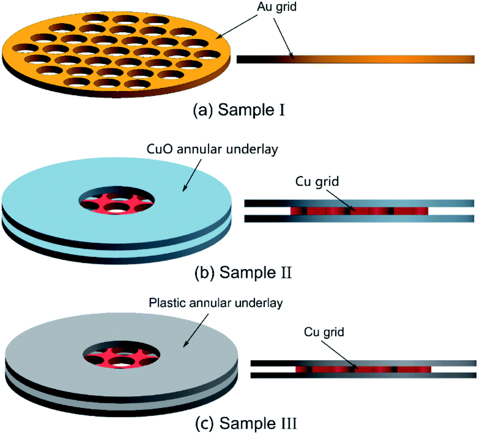 | ||
| Fig. 4 Schematic diagrams of sandwich-like TEM grids with controlled charge transport resistance via adapting different annular underlays: (a) Au grid, (b) Cu grid with Cu annular underlay, surface oxidized at 300 °C, and (c) Cu grid with plastic annular underlay. | ||
A sample with high resistance was specially focused since its enhanced charge resistance nature provides magnified influence on the charging-induced imaging instability. It thus allows us to complete the quantitative analysis on the image drift in a shorter time, so as to exclude the interference from the sample damage issue on the measurement. In particular, the carbon film region is focused for analysis on the vertical drift for the Z axis. For the horizontal drift in the sample plane, the TEM gird was loaded with nanoparticles, serving as the target to be tracked via the image recognition algorithm. To enlarge the influence of charging effects along the sample plane, a strategy of instant charging was utilized to initiate the drift process, where the grid was quickly charged in large quantity by directly irradiating the plastic underlays with the beam and back to track imaging drift on the sample region. This instant charging makes the following horizontal drifting analysis performed in an overall discharging background.
Besides, the in situ dynamic drift process is displayed in Movie S1† under the in situ TEM mode on an aberration-corrected environmental TEM (Thermo Fisher Scientific Titan Themis ETEM G3), equipped with a 4k × 4k resolution camera, recorded at a rate of 2 frames per s (OneView IS from Gatan Ametech Co., Ltd.). TEM experiments were conducted at 80 kV. The dose rate was 725 e Å−2 s and coefficient of spherical aberration was Cs = −2 μm. To calculate defocus variation, one high-resolution TEM (HRTEM) image was captured for the amorphous carbon film supported on the grid. After the irradiation of the electron beam for 5 min, another HRTEM image was acquired at the same location to reflect the change of defocus.
For the analysis of microscopy data after the experiments, an algorithm was developed for precisely calculating the defocus value of imaging via the quantitative fitting of contrast transfer function (CTF) that was extracted from the frequency pattern of each HRTEM image. Moreover, the displacement of imaging along the XY plane of a sample was monitored by tracking the feature of nanoparticles in the image series using OpenCV algorithm.
Author contributions
Z. Y. Z. and W. L. conceived the projects. L. H. W. and D. D. L. performed the experiments and analyzed the charging mechanism. F. Z., Z. H. J., Y. Q. L. and Z. B. Y. conducted the algorithm of defocus estimation. L. H. W. wrote the paper. W. L., J. F. C. and Z. Y. Z. modified the syntax. All authors discussed the results and commented on the manuscript.Conflicts of interest
There are no conflicts of interest to declare.Acknowledgements
The authors acknowledge the financial support from the National Key R&D Program of China (2018YFA0703400), National Natural Science Foundation of China (22072150), CAS Youth Innovation Promotion Association (2019190), the Xinghai Science Funds for Distinguished Young Scholars and Thousand Youth Talents at Dalian University of Technology, and the Collaborative Innovation Center of Major Machine Manufacturing in Liaoning.References
- M. Harider, S. Uhlemann, E. Schwan, H. Rose, B. Kabius and K. Urban, Nature, 1998, 392, 768–769 CrossRef.
- H. Rose, Optik, 1990, 85, 19–24 Search PubMed.
- A. Musashino, JEOL Application Note EM2020-09E: Achieves the world’s highest level resolution with newly developed atomic resolution analytical electron microscope “GRAND ARM™2”, 2020, https://www.jeol.co.jp/en/applications/detail/1974.html Search PubMed.
- R. F. Egerton, Micron, 2019, 119, 72–87 CrossRef CAS PubMed.
- R. Wernet, D. Nazarenus and M. Seipenbusch, J. Aerosol Sci., 2017, 110, 1–10 CrossRef CAS.
- J. Cazaux, Scanning, 2004, 26, 181–203 CrossRef PubMed.
- J. Cazaux, Nucl. Instrum. Methods Phys. Res., Sect. B, 2006, 244, 307–322 CrossRef CAS.
- A. Melchinger and S. Hofmann, J. Appl. Phys., 1995, 78, 6224–6232 CrossRef CAS.
- S. Hettler, E. Kano, M. Dries, D. Gerthsen, L. Pfaffmann, M. Bruns, M. Beleggia and M. Malac, Ultramicroscopy, 2018, 184, 252–266 CrossRef CAS PubMed.
- J. Cazaux, Eur. Phys. J.: Appl. Phys., 2001, 15, 167–172 CrossRef CAS.
- J. Cazaux, Microsc. Microanal., 2004, 10, 670–684 CrossRef CAS.
- O. Jbara, S. Fakhfakh and M. Belhaj, Nucl. Instrum. Methods Phys. Res., Sect. B, 2002, 194, 302–310 CrossRef CAS.
- J. Barthel and A. Thust, Ultramicroscopy, 2010, 111, 27–46 CrossRef CAS PubMed.
- A. R. Lupini and S. J. Pennycook, J. Electron Microsc., 2008, 57, 195–201 Search PubMed.
- A. R. Lupini, P. Wang and P. D. Nellist, Ultramicroscopy, 2010, 110, 891–898 CrossRef CAS PubMed.
- M. Vulovic, P. L. Brandt, R. B. G. Ravelli, A. J. Koster, L. J. van Vliet and B. Rieger, 2010 7th IEEE International Symposium on Biomedical Imaging, From Nano To Macro, 2010, pp. 1121–1124 Search PubMed.
- M. Vulovic, E. Franken, R. B. G. Ravelli, L. J. van Vliet and B. Rieger, Ultramicroscopy, 2012, 116, 115–134 CrossRef CAS.
- O. L. Krivanek, Optik, 1976, 45, 97–101 Search PubMed.
Footnote |
| † Electronic supplementary information (ESI) available. See DOI: 10.1039/d1na00140j |
| This journal is © The Royal Society of Chemistry 2021 |