
 Open Access Article
 This Open Access Article is licensed under a Creative Commons Attribution-Non Commercial 3.0 Unported Licence
Mechanically rollable photodetectors enabled by centimetre-scale 2D MoS2 layer/TOCN composites†
Changhyeon
Yoo
a,
Tae-Jun
Ko
a,
Sang Sub
Han
ac,
Mashiyat Sumaiya
Shawkat
 ad,
Kyu Hwan
Oh
c,
Bo Kyoung
Kim
e,
Hee-Suk
Chung
e and
Yeonwoong
Jung
*abd
ad,
Kyu Hwan
Oh
c,
Bo Kyoung
Kim
e,
Hee-Suk
Chung
e and
Yeonwoong
Jung
*abd
aNanoScience Technology Center, University of Central Florida, Orlando, Florida 32826, USA. E-mail: yeonwoong.jung@ucf.edu
bDepartment of Materials Science and Engineering, University of Central Florida, Orlando, Florida 32816, USA
cDepartment of Materials Science and Engineering, Seoul National University, Seoul, 08826, South Korea
dDepartment of Electrical and Computer Engineering, University of Central Florida, Orlando, Florida 32816, USA
eAnalytical Research Division, Korea Basic Science Institute, Jeonju 54907, South Korea
First published on 6th April 2021
Abstract
Two-dimensional (2D) molybdenum disulfide (MoS2) layers are suitable for visible-to-near infrared photodetection owing to their tunable optical bandgaps. Also, their superior mechanical deformability enabled by an extremely small thickness and van der Waals (vdW) assembly allows them to be structured into unconventional physical forms, unattainable with any other materials. Herein, we demonstrate a new type of 2D MoS2 layer-based rollable photodetector that can be mechanically reconfigured while maintaining excellent geometry-invariant photo-responsiveness. Large-area (>a few cm2) 2D MoS2 layers grown by chemical vapor deposition (CVD) were integrated on transparent and flexible substrates composed of 2,2,6,6-tetramethylpiperidine-1-oxyl (TEMPO)-oxidized cellulose nanofibers (TOCNs) by a direct solution casting method. These composite materials in three-dimensionally rollable forms exhibited a large set of intriguing photo-responsiveness, well preserving intrinsic opto-electrical characteristics of the integrated 2D MoS2 layers; i.e., light intensity-dependent photocurrents insensitive to illumination angles as well as highly tunable photocurrents varying with the rolling number of 2D MoS2 layers, which were impossible to achieve with conventional photodetectors. This study provides a new design principle for converting 2D materials to three-dimensional (3D) objects of tailored functionalities and structures, significantly broadening their potential and versatility in futuristic devices.
Introduction
In recent years, two-dimensional (2D) transition metal dichalcogenide (TMD) layers have been extensively explored for unconventional optoelectronics owing to their extraordinary material properties coupled with van der Waals (vdW) bonding-enabled relaxed assembly.1–9 Such advantages provide opportunities for realizing “mechanically reconfigurable” devices of exotic structures achieving an unprecedented level of multi-dimensional flexibility; i.e., devices capable of reversibly accommodating severe mechanical deformation upon external stimuli and preserving their intrinsic opto-electrical characteristics, which is impossible with conventional bulky and rigid 3D semiconductors.2,10–12 Earlier studies focused on incorporating various TMDs into conventional 3D semiconductors, realizing photo-responsive 2D/3D heterojunctions.13–17 Particularly, 2D MoS2 layers are attractive as active device components owing to their tunable bandgap energy matching the visible-to-near infrared spectral range accompanying high carrier mobility.2,18–20 Furthermore, they exhibit extremely large in-plane strain limits and mechanical robustness suitable for achieving mechanical reconfigurability; e.g., high breaking strength of >20 GPa at a strain range of 6–11% even outperforming polyimide (PI) and polydimethylsiloxane (PDMS), the two most commonly employed substrates for flexible electronic devices.21 Amongst a variety of reconfigurable structures, mechanically “rollable” electronic devices incorporating three-dimensionally structured 2D layers are proposed to be promising for tuning and/or improving opto-electrical performances.22 Some proof-of-concept demonstrations have been made by converting conventional 3D semiconductors such as silicon (Si) and III–V compounds into 3D tubular forms. These include optical resonators,23 actuators,24 and resistive random access memories25 in rollable forms, while their mechanical reconfigurability is significantly limited due to the intrinsic rigidity of 3D materials. In addition to considering active device components, identifying suitable substrate materials for reconfigurable devices is also essential since they often demand extraordinary functionalities, e.g., a combination of large mechanical resilience and bio-compatibility for human–machine interfaces and e-skin devices.2,10,26–28 Cellulose is one of the most abundant natural polymers represented by ∼1.5 trillion tons of total biomass output per year and is naturally renewable and biodegradable.29–32 Particularly, TEMPO-oxidized cellulose nanofibers (CNFs), i.e., TOCNs, have been identified to possess an abundant set of superior properties including low density (∼1.5 g cm−3) and high mechanical stiffness and elasticity, as well as excellent optical transparency (∼90%) and thermal stability (>180 °C).30,33–36 Recently, integration of large-area CVD-2D MoS2 layers onto TOCN substrates was demonstrated to realize unconventional transient and biodegradable characteristics,12,37,38 providing numerous opportunities for novel device functionalities.In this work, we developed MoS2/TOCN composite materials and explored them for mechanically reconfigurable photodetectors. Centimetre-scale CVD-2D MoS2 layers were directly integrated on TOCN substrates via a water-assisted drop-casting method and were subsequently rolled into 3D tubular forms with preserved structural and optical integrity. Electrical responses of these 3D-converted 2D materials were evaluated under controlled optical illumination, which yielded tunable photo-responsiveness varying with the geometry of rolled 2D layers.
Experimental
CVD growth of centimetre-scale 2D MoS2 layers
SiO2/Si wafers (300 nm thickness) were cleaned by ultrasonication in acetone, isopropyl alcohol (IPA), and deionized (DI) water to remove any organic impurities. Mo seeds of controlled thickness were deposited on the wafers by using an e-beam evaporator (Thermionics VE-100) at a deposition rate of 0.05–0.12 Å s−1 and at a base pressure below 5.5 × 10⁻⁶ Torr. The Mo-deposited wafers were kept at the centre of a CVD furnace chamber (Lindberg/Blue M Mini-Mite) along with sulfur (S) powder (≥99.5%, Sigma-Aldrich) placed on an alumina boat at the upstream side. The CVD chamber was pumped down to 40 mTorr, and ultra-pure argon (Ar) gas was supplied at a flow rate of 100 sccm (standard cubic centimetre per minute). Subsequently, the CVD furnace was heated up to 800 °C in ∼50 min and was maintained at that temperature for another ∼50 min, followed by natural cooling to room temperature.Integration of 2D MoS2 layers on TOCN substrates via solution-casting
Commercially available slurry of TOCN (CELLULOSELAB) in water (1 wt%) was mixed with DI water. After dilution to 0.5 wt%, it was subsequently sonicated for a few hours, and the final dispersion was directly poured onto a SiO2/Si wafer covered with as-grown 2D MoS2 layers. The prepared sample was dried at room temperature for >48 hours until the casted TOCN was thoroughly dried and turned transparent. After the drying stage, the TOCN-attached 2D MoS2 layers were gently delaminated from the SiO2/Si growth wafers.Opto-electrical measurements
Electrical measurements were performed using an HP 4156A semiconductor parameter analyser with a home-built probe station. Photo-response measurements of rolled MoS2/TOCN photodetectors were performed using an M625L4-C2 – Red (625 nm) Thorlabs collimated LED in the dark and upon illumination. Optical absorbances of MoS2/TOCN and TOCN samples were characterized by UV-vis spectroscopy (Cary 300 Win UV-vis spectrometer) in the wavelength range of 200–800 nm.Results and discussion
We fabricated mechanically reconfigurable 3D tubular photodetectors by “rolling up” centimetre-scale CVD-2D MoS2 layers integrated on TOCN substrates, as illustrated in Fig. 1a. Fabrication starts with the wafer-scale CVD growth of 2D MoS2 layers with a typical lateral dimension of ∼10 cm × 2 cm on top of a SiO2/Si wafer.11,39–41 CVD growth is performed by thermally sulfurizing Mo seed films of controlled thickness (typically, ∼1–6 nm) following the procedures described in the previous Experimental section. The thickness of the 2D MoS2 layers obtained from the CVD sulfurization of Mo films was consistent with that reported in our previous studies and others, with a linear increase of 3–3.5 times from the Mo-to-2D MoS2 conversion.12,39,41 Separately, a TOCN dispersion is prepared using commercially available TOCN slurry in water (1 wt%) by employing the recipe developed in our previous report.12 Subsequently, it is directly drop-casted onto a SiO2/Si wafer with as-grown 2D MoS2 layers and is subsequently dried in air at room temperature. The dried TOCN-attached 2D MoS2 layers are manually peeled off from the growth wafer, followed by deposition of gold (Au; ∼60 nm thickness) top electrodes. Lastly, the Au-2D MoS2 layer-integrated TOCN is manually rolled up using a cylindrical rod, yielding a mechanically reconfigurable and rollable MoS2/TOCN composite for opto-electrical measurements. It is worth mentioning that we previously demonstrated the water-assisted facile delamination of wafer-scale 2D MoS2 layers from SiO2/Si growth wafers and their integration onto various exotic substrates.11,12Fig. 1b shows optical images of original SiO2/Si growth wafers with as-grown 2D MoS2 layers removed (left) and identical 2D MoS2 layers transferred and integrated on a TOCN substrate (right). The images confirm that the 2D MoS2 layers on the TOCN substrate precisely reproduce the original shape and size of the growth wafers, confirming the excellent fidelity of water-assisted delamination. Furthermore, the TOCN substrate – the area within the red dotted lines – is optically transparent, rendering suitability for opto-electrical studies, which is verified in the next section. Fig. 1c shows a side-view image of a representative Au electrode-contacted MoS2/TOCN composite manually rolled up by a cylindrical rod, presenting a well-sustained tubular structure. Fig. 1d shows an image of the composite before its rolling as well as an enlarged microscopy image (red box) corresponding to the device area of 2D MoS2 layers with a channel length of ∼500 μm.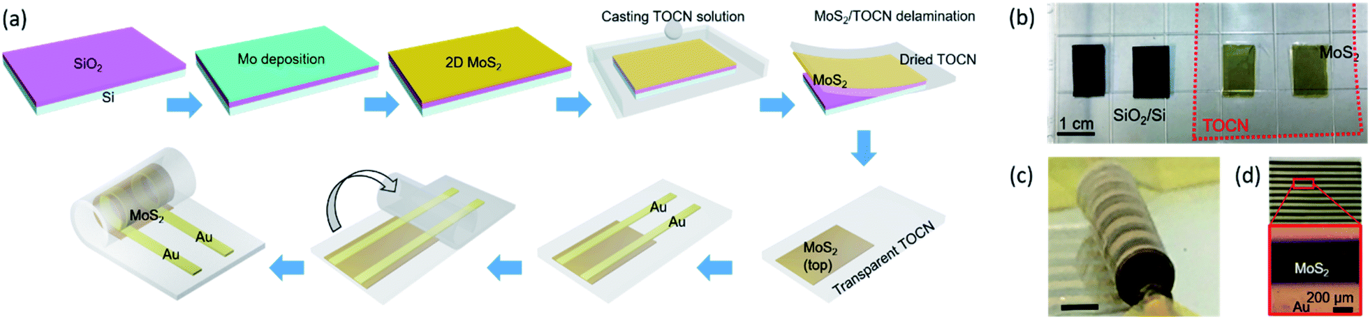 | ||
| Fig. 1 (a) Illustrative description of the fabrication process of rollable MoS2/TOCN composites. (b) Optical image of original SiO2/Si growth wafers (left) and 2D MoS2 layers integrated on a TOCN substrate after delamination from the wafers (right). (c) Optical image of a rolled MoS2/TOCN composite with top Au electrodes. The scale bar is 0.5 cm. (d) Optical image of a Au electrode contacted-MoS2/TOCN composite in the flattened form and its enlarged view to visualize device components. | ||
Prior to investigating photo-responsive performances of MoS2/TOCN composites, we first characterized the material quality of 2D MoS2 layers integrated on TOCN substrates before their rolling. Fig. 2a shows scanning electron microscope (SEM) images of a bare TOCN (left) and 2D MoS2 layers (Mo; 1 nm seed) integrated on it (right). The SEM image of the bare TOCN and its magnified view (yellow box and inset) reveals its fibrous and porous structure composed of homogeneously networked individual CNFs. Fig. 2b shows the Raman spectroscopy profile of the MoS2/TOCN sample, revealing two characteristic peaks corresponding to the in-plane E12g and out-of-plane A1g oscillation modes of 2D MoS2 layers in agreement with previous reports.41,42 Additional structural characterization data including transmission electron microscopy (TEM) images and atomic force microscopy (AFM) height profiles are presented in Fig. S1, ESI.† Optical properties of MoS2/TOCN samples are essential characteristics for photodetection applications and were characterized by ultraviolet (UV)-visible (vis) spectroscopy and optical microscopy. The top panel in Fig. 2c shows optical images of 2D MoS2 layers integrated on TOCN substrates, prepared with Mo seeds of various thicknesses, i.e., 1, 4, and 6 nm. The thickness of the resulting 2D MoS2 layers was previously confirmed to be 3–3.5 times larger than that of deposited Mo seed layers.12,39,41 The images show that the optical color of 2D MoS2 layers gradually becomes darker with increasing Mo thickness. The bottom panel in Fig. 2c presents UV-vis optical transmittance profiles of MoS2/TOCN samples with varying Mo thickness as well as a bare TOCN substrate. The spectral profiles confirm high optical transparency of the TOCN, i.e., ∼90% transmittance in the visible range of ∼350–800 nm wavelength. MoS2/TOCN samples exhibit reduced optical transmittance, which becomes more pronounced with increasing Mo thickness; for instance, the optical transmittances for the samples obtained with Mo seeds of 1, 4, and 6 nm determined at 625 nm wavelength are 74.84, 65.49, and 57.69%, respectively. Furthermore, the shapes of the UV-vis spectral profiles are consistent with previous observations with thickness-varying 2D MoS2 layers integrated on other optically transparent substrates.43–46 Detailed optical characteristics of integrated 2D MoS2 layers were further analysed by developing Tauc plots from the UV-vis spectra,47,48 as shown in Fig. 2d. The plots reveal that the bandgap energies are in the range of ∼1.28–1.41 eV for the 2D MoS2 layers with a thickness of ∼3.5–21 nm (ref. 41) (obtained from Mo seeds of 1–6 nm, respectively). These values are in good agreement with the bandgap energies of multilayer 2D MoS2 of comparable thickness reported in the literature,2,47,48 confirming that 2D MoS2 layers well-retained their intrinsic opto-electrical characteristics even after integration on TOCN substrates. The inset graph in Fig. 2d shows the corresponding absorbance spectra manifested by (αhν)1/2 where α is the optical absorption coefficient and hν is the photon energy. After confirming the intrinsic opto-electrical properties of MoS2/TOCN composites, we then explored their photo-responsiveness for rollable photodetector applications. Fig. 3a shows the current–voltage (I–V) plot of a rolled-up MoS2/TOCN sample (lower inset) in a two-terminal configuration (upper inset) exhibiting ohmic-like transport. Photo-responsive characteristics of three-dimensionally rolled-up samples were characterized by using a collimated 625 nm light-emitting diode (LED; THORLABS) with varying illumination angles of 0, 45, and 90°, as illustrated in Fig. 3b. The inset presents a side-view image of a representative sample. Fig. 3c shows plots of a time-dependent change in photocurrent induced by periodic illumination from a 625 nm LED (intensity: 488 W m−2), obtained from an identical sample prepared with Mo of 6 nm. Illumination was performed at three different angles of 0, 45, and 90° as shown in Fig. 3b, maintaining an identical illumination distance irrespective of the angle variation. It is apparent that the photocurrent periodically increases (and decreases) when the LED is turned on (and off), which is well-retained at varying illumination intervals of 5 seconds and 10 seconds. The results indicate that the 2D MoS2 layers integrated on TOCN substrates are highly photo-responsive owing to their well-preserved semiconducting characteristics (Fig. 2b) irrespective of their 3D mechanical deformation. Furthermore, the TOCN substrate exhibits high optical transparency (Fig. 2c) which negligibly affects the photo-responsiveness while sustaining the mechanical robustness of the rolled 2D MoS2 layers. We compared photo-responsive characteristics of an identical sample in two different states of unrolled vs. rolled (see Fig. S2, ESI†). A slight decrease in the maximum photocurrent was observed in the rolled sample, while the average I0 remained nearly constant. Such reduction in the photocurrent is mainly attributed to the reduced optical absorption toward the edge of the illuminated area of the sample due to its large bending curvature. Nevertheless, the potential roles of intrinsic strain effects in altering the band structures of 2D MoS2 layers (toward increasing their photocurrents) cannot be completely ruled out.49–51 Exact clarification of the underlying mechanism needs further studies. After confirming the 3D photo-responsiveness from the horizontal (0°)-to-vertical (90°) illumination, we further characterized the photo-responsiveness of other samples by varying illumination intensities at a fixed illumination angle of 0°. Fig. 3d shows representative plots of intensity-dependent photocurrent with varying intensities from 157 to 488 W m−2, obtained from a sample different from Fig. 3c with a different illumination distance. The results show a well-resolved increase of photocurrent with increasing intensity, which is highly reversible upon periodic illumination at an interval of 5 seconds. Fig. 3e presents plots of intensity-dependent photocurrent ratios (Iphoto/I0) for samples prepared with two different Mo thicknesses of 1 and 4 nm. Iphoto and I0 are the currents with and without illumination, respectively. The Mo 4 nm sample exhibits higher Iphoto/I0 values through the entire intensity range, which is mainly attributed to the higher absorption of photons in samples of a larger thickness (Fig. 2c), although the intrinsic dark current of the samples increases with increasing thickness (see Fig. S3, ESI†). Furthermore, both samples show a highly linear relationship of intensity vs. Iphoto/I0, indicating their reliable photo-responsiveness and excellent mechanical adaptability. Fig. 3f presents the intensity-dependent photo-responsivity, R, which is a key parameter to evaluate the performances of photodetectors. Photo-responsivity, R is defined as;
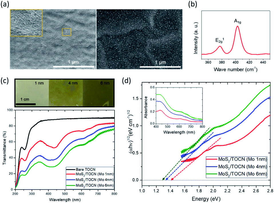 | ||
| Fig. 2 (a) SEM images of a bare TOCN substrate (left) and 2D MoS2 layers integrated on it (right). (b) Raman spectrum obtained from CVD-grown 2D MoS2 layers integrated on a TOCN substrate denoting their characteristic peaks. (c) Optical images of 2D MoS2 layers integrated on TOCN substrates prepared with Mo seeds of 1, 4, and 6 nm thickness (top) and their corresponding UV-vis optical transmittance spectra (bottom). (d) Tauc plots for MoS2/TOCN composites with varying Mo thickness and their corresponding optical absorbance spectra (inset). | ||
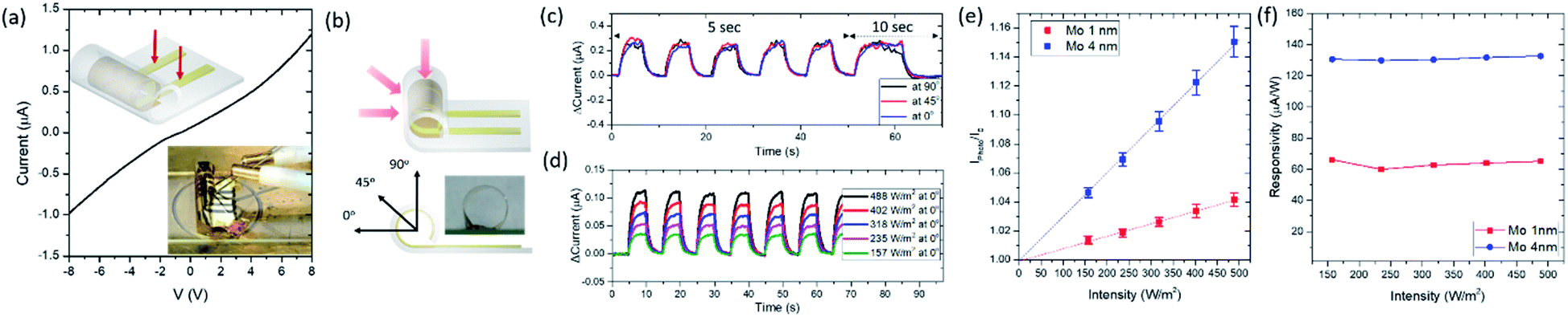 | ||
| Fig. 3 (a) Two-terminal I–V characteristics of a MoS2/TOCN tubular device along with its schematic illustration (upper inset) and camera image (lower inset). (b) Illustrations for angle-varying optical illumination onto a MoS2/TOCN tubular device. The inset shows a side-view image of a representative device. (c) Time-dependent photocurrents from an identical sample under periodic illumination with varying illumination angles. (d) Time-dependent photocurrents from another sample under periodic illumination with varying illumination intensities. (e) Intensity-dependent Iphoto/I0 for two different samples prepared with Mo seed thicknesses of 1 and 4 nm measured at 8 V. (f) Intensity-dependent photo-responsivity obtained from the same sample in (e). | ||
Encouraged by their intrinsically excellent photo-responsiveness, we further explored the MoS2/TOCN samples for mechanically tunable photodetection by modulating their degree of rolling. Fig. 4a demonstrates that as-prepared MoS2/TOCN samples can be manually rolled up using a rolling bar, which precisely controls their rolling numbers. Fig. 4b illustrates a side view of an identical sample with two different rolling numbers under horizontal illumination. Note that the illumination distance – i.e., the distance between the LED source (625 nm wavelength) and the outermost sample surface – is maintained to be identical for both cases. Fig. 4c left panel presents photo-responsiveness of an identical MoS2/TOCN sample (Mo: 6 nm thickness) with rolling numbers of one and two, corresponding to the optical images on the right panel. Interestingly, a higher (∼25% increase) photocurrent was observed when the sample was rolled up twice, possessing a smaller rolling diameter despite the larger degree of mechanical deformation. This enhancement is attributed to the combined result of (1) an increased active area in absorbing illumination within the 2D layers and (2) Reduced illumination distance for the inner rolls absorbing the photons transmitted from the outermost layers. Note that the 2D layers with two rolls offer secondary active areas of the “inner” rolls to additionally absorb photons transferred from the “outer” rolls. Furthermore, the intrinsically large optical transmittance of MoS2/TOCN layers (e.g., ∼70% transmittance at 625 nm wavelength in Fig. 2c) allows for the efficient transmittance of incident photons through them. We also tested the performance limit of this rolling approach for tunable photodetection by rolling up two different samples with similar diameters. Fig. 4d left panel illustrates schematics of tightly rolled samples with three and four rolling numbers, and Fig. 4d right panel presents time-dependent photocurrents corresponding to them – the samples are different from Fig. 4c. Both samples show well-maintained photo-responsiveness under vertical illumination. The slightly lower photocurrent observed with the sample with four rolls is possibly attributed to the combined result of intrinsic strain effects on altering the band structure of 2D MoS2 layers49–51 as well as the reduced optical transmittance with increasing rolling number and bending curvatures. Nevertheless, exact clarification of the underlying mechanism warrants further investigation. Similar behaviours were observed in the samples prepared with Mo of 1 and 6 nm (see Fig. S5, ESI†). We believe that the overall photo-responsiveness (particularly, responsivity) of MoS2/TOCN can be further enhanced by improving (a) the crystallinity of large-area 2D MoS2 layers by adopting advanced growth methods such as metal organic CVD (MOCVD) and (b) the MoS2/TOCN interfacial homogeneity through a more controlled layer delamination/transfer method.
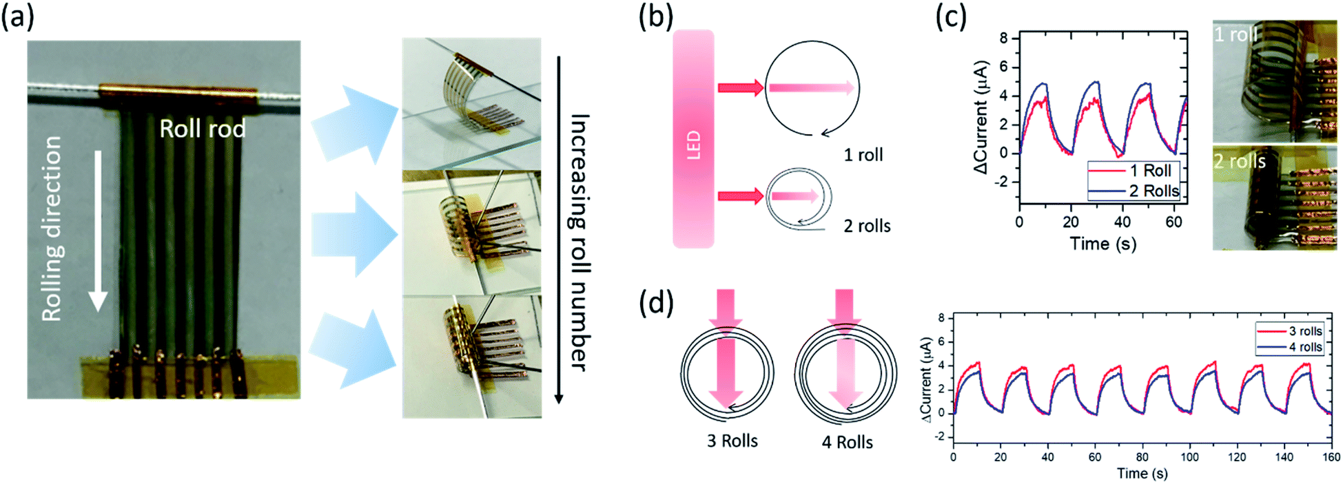 | ||
| Fig. 4 (a) Mechanical rolling of a tubular MoS2/TOCN device using a rolling rod (left panel) to control its roll number (right panel). (b) Schematics of horizontal illumination onto a tubular MoS2/TOCN device with two different roll numbers. (c) Time-dependent photocurrents obtained from an identical sample with roll numbers of 1 and 2 (left panel) and the camera images of the corresponding device (right panel) at 5 V. (d) Schematics of vertical illumination onto two different tubular MoS2/TOCN devices with different roll numbers (left panel) and the corresponding time-dependent photocurrents (right panel). | ||
Lastly, we demonstrate the mechanical reconfigurability of MoS2/TOCN rollable photodetectors by testing their flexibility and elasticity. Fig. 5 shows time-lapsed snapshot images of a previously rolled MoS2/TOCN sample which is initially held by a rolling rod. Once the rolling rod is released from its initially flattened state, the sample quickly returns to its rolled state in less than one second (see Video S1, ESI†). Once the device is rolled up again, it still exhibits well-preserved opto-electrical characteristics confirming excellent reversibility. We tested the stability of the device by repeatedly unrolling/rolling the Mo 6 nm sample, as shown in Fig. 5. The maximum photocurrent, ΔImax (Iphoto,max − I0), was observed to decrease by less than ∼20% of its initial value after spontaneous rolling of the device up to 100 cycles (see Fig. S6, ESI†). Therefore, rolling/unrolling multiple times was possible, yielding no significant mechanical degradation (e.g., cracks) in the sample (see Fig. S7, ESI†).
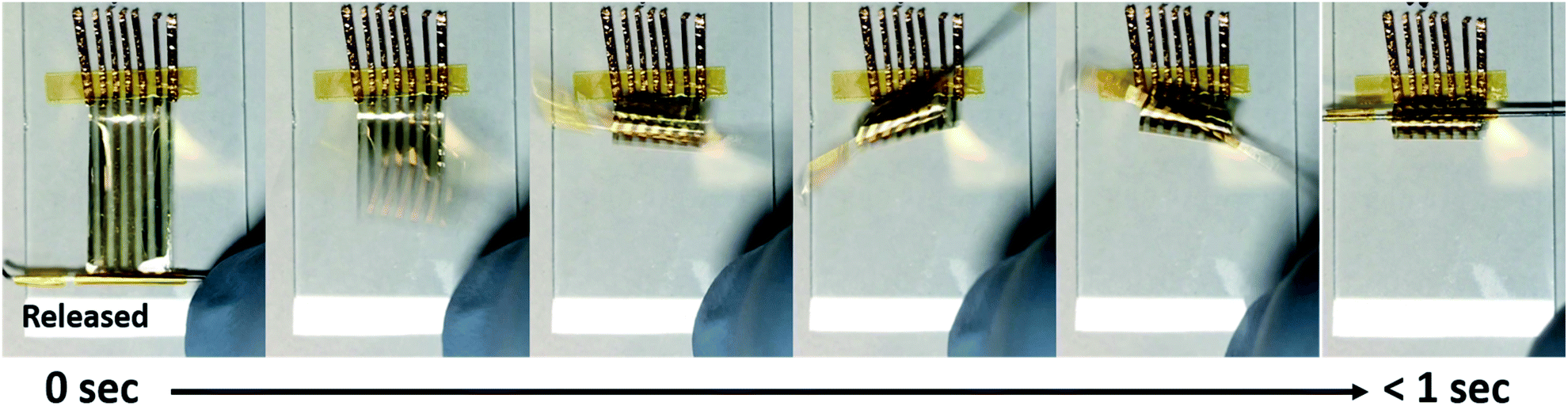 | ||
| Fig. 5 Time-lapsed snapshot images of a tubular MoS2/TOCN device spontaneously changing from the flattened state (left) to the rolled state (right) demonstrating its flexibility and elasticity. | ||
Conclusions
In conclusion, we integrated large-area CVD-2D MoS2 layers on optically transparent TOCN substrates and identified their mechanical deformation-driven opto-electrical properties. By rolling up MoS2/TOCN composites in a controlled manner, we developed 3D tubular photodetectors operated by photo-responsive 2D MoS2 layers and identified their highly tunable photocurrents with varying geometrical parameters. The method to convert 2D MoS2 layers into 3D rollable forms developed in this work is believed to be applicable to other 2D TMD layers. Furthermore, the design principle and working mechanism of 2D layer-based 3D photodetectors can further help explore 2D TMD layer-based unconventional devices in mechanically reconfigurable forms.Author contributions
Y. J. conceived the project and directed it. C. Y. prepared MoS2/TOCN samples and characterized their photo-responsive characteristics. T.-J. K. performed optical characterization of the samples and participated in the sample preparation. S. S. H. assisted in sample preparation under the guidance of K. H. O. M. S. S. assisted in photo-responsiveness characterization. B. K. K., and H.-S. C. performed structural characterization of the samples. C. Y. and Y. J. wrote the manuscript with inputs from all the authors.Conflicts of interest
The authors declare no competing financial interests.Acknowledgements
Y. J. acknowledges financial support from the National Science Foundation (CMMI-1728390), the Korea Institute of Energy Technology Evaluation and Planning (KETEP) and the Ministry of Trade, Industry & Energy (MOTIE) of the Republic of Korea (No. 20173010013340), as well as the VPR Advancement of Early Career Researchers award from the University of Central Florida.References
- D. Akinwande, N. Petrone and J. Hone, Nat. Commun., 2014, 5, 5678 CrossRef CAS PubMed.
- T.-J. Ko, M. Wang, C. Yoo, E. Okogbue, M. A. Islam, H. Li, M. S. Shawkat, S. S. Han, K. H. Oh and Y. Jung, J. Phys. D: Appl. Phys., 2020, 53, 313002 CrossRef CAS.
- S. J. Kim, K. Choi, B. Lee, Y. Kim and B. H. Hong, Annu. Rev. Mater. Res., 2015, 45, 63–84 CrossRef CAS.
- M. Wang, H. Li, T.-J. Ko, M. Sumaiya Shawkat, E. Okogbue, C. Yoo, S. S. Han, M. A. Islam, K. H. Oh and Y. Jung, J. Mater. Res., 2020, 1–19, DOI:10.1557/jmr.2020.27.
- H. Zhang, ACS Nano, 2015, 9, 9451–9469 CrossRef CAS PubMed.
- C. Tan, X. Cao, X.-J. Wu, Q. He, J. Yang, X. Zhang, J. Chen, W. Zhao, S. Han, G.-H. Nam, M. Sindoro and H. Zhang, Chem. Rev., 2017, 117, 6225–6331 CrossRef CAS PubMed.
- K. F. Mak, C. Lee, J. Hone, J. Shan and T. F. Heinz, Phys. Rev. Lett., 2010, 105, 136805 CrossRef PubMed.
- Q. H. Wang, K. Kalantar-Zadeh, A. Kis, J. N. Coleman and M. S. Strano, Nat. Nanotechnol., 2012, 7, 699–712 CrossRef CAS PubMed.
- M. Chhowalla, H. S. Shin, G. Eda, L.-J. Li, K. P. Loh and H. Zhang, Nat. Chem., 2013, 5, 263–275 CrossRef PubMed.
- L. Gao, Small, 2017, 13, 1603994 CrossRef PubMed.
- J. H. Kim, T.-J. Ko, E. Okogbue, S. S. Han, M. S. Shawkat, M. G. Kaium, K. H. Oh, H.-S. Chung and Y. Jung, Sci. Rep., 2019, 9, 1641 CrossRef PubMed.
- C. Yoo, M. G. Kaium, L. Hurtado, H. Li, S. Rassay, J. Ma, T.-J. Ko, S. S. Han, M. S. Shawkat, K. H. Oh, H.-S. Chung and Y. Jung, ACS Appl. Mater. Interfaces, 2020, 12, 25200–25210 CrossRef CAS PubMed.
- C. Jia, D. Wu, E. Wu, J. Guo, Z. Zhao, Z. Shi, T. Xu, X. Huang, Y. Tian and X. Li, J. Mater. Chem. C, 2019, 7, 3817–3821 RSC.
- Y. Wang, X. Huang, D. Wu, R. Zhuo, E. Wu, C. Jia, Z. Shi, T. Xu, Y. Tian and X. Li, J. Mater. Chem. C, 2018, 6, 4861–4865 RSC.
- Z. Lou, L. Zeng, Y. Wang, D. Wu, T. Xu, Z. Shi, Y. Tian, X. Li and Y. H. Tsang, Opt. Lett., 2017, 42, 3335–3338 CrossRef CAS PubMed.
- D. Wu, J. Guo, J. Du, C. Xia, L. Zeng, Y. Tian, Z. Shi, Y. Tian, X. J. Li, Y. H. Tsang and J. Jie, ACS Nano, 2019, 13, 9907–9917 CrossRef CAS PubMed.
- D. Wu, Z. Lou, Y. Wang, Z. Yao, T. Xu, Z. Shi, J. Xu, Y. Tian, X. Li and Y. H. Tsang, Sol. Energy Mater. Sol. Cells, 2018, 182, 272–280 CrossRef CAS.
- M. R. Islam, N. Kang, U. Bhanu, H. P. Paudel, M. Erementchouk, L. Tetard, M. N. Leuenberger and S. I. Khondaker, Nanoscale, 2014, 6, 10033–10039 RSC.
- K. K. Kam and B. A. Parkinson, J. Phys. Chem., 1982, 86, 463–467 CrossRef CAS.
- A. Kuc, N. Zibouche and T. Heine, Phys. Rev. B: Condens. Matter Mater. Phys., 2011, 83, 245213 CrossRef.
- S. Bertolazzi, J. Brivio and A. Kis, ACS Nano, 2011, 5, 9703–9709 CrossRef CAS PubMed.
- X. Zhou, Z. Tian, H. J. Kim, Y. Wang, B. Xu, R. Pan, Y. J. Chang, Z. Di, P. Zhou and Y. Mei, Small, 2019, 15, 1902528 CrossRef CAS PubMed.
- D. R. Kazanov, A. V. Poshakinskiy, V. Y. Davydov, A. N. Smirnov, I. A. Eliseyev, D. A. Kirilenko, M. Remškar, S. Fathipour, A. Mintairov, A. Seabaugh, B. Gil and T. V. Shubina, Appl. Phys. Lett., 2018, 113, 101106 CrossRef.
- B. Xu, Z. Tian, J. Wang, H. Han, T. Lee and Y. Mei, Sci. Adv., 2018, 4, eaap8203 CrossRef PubMed.
- X. Hou, R. Pan, Q. Yu, K. Zhang, G. Huang, Y. Mei, D. W. Zhang and P. Zhou, Small, 2019, 15, 1803876 CrossRef PubMed.
- M. L. Hammock, A. Chortos, B. C. K. Tee, J. B. H. Tok and Z. Bao, Adv. Mater., 2013, 25, 5997–6038 CrossRef CAS PubMed.
- T. Sekitani and T. Someya, MRS Bull., 2012, 37, 236–245 CrossRef.
- X. Wang, L. Dong, H. Zhang, R. Yu, C. Pan and Z. L. Wang, Adv. Sci., 2015, 2, 1500169 CrossRef PubMed.
- R. J. Moon, A. Martini, J. Nairn, J. Simonsen and J. Youngblood, Chem. Soc. Rev., 2011, 40, 3941–3994 RSC.
- S. J. Eichhorn, Soft Matter, 2011, 7, 303–315 RSC.
- J.-H. Kim, B. S. Shim, H. S. Kim, Y.-J. Lee, S.-K. Min, D. Jang, Z. Abas and J. Kim, International Journal of Precision Engineering and Manufacturing-Green Technology, 2015, 2, 197–213 CrossRef.
- W. Kang, C. Yan, C. Y. Foo and P. S. Lee, Adv. Funct. Mater., 2015, 25, 4203–4210 CrossRef CAS.
- T. Saito, S. Kimura, Y. Nishiyama and A. Isogai, Biomacromolecules, 2007, 8, 2485–2491 CrossRef CAS PubMed.
- A. Isogai, T. Saito and H. Fukuzumi, Nanoscale, 2011, 3, 71–85 RSC.
- Y. H. Jung, T.-H. Chang, H. Zhang, C. Yao, Q. Zheng, V. W. Yang, H. Mi, M. Kim, S. J. Cho, D.-W. Park, H. Jiang, J. Lee, Y. Qiu, W. Zhou, Z. Cai, S. Gong and Z. Ma, Nat. Commun., 2015, 6, 7170 CrossRef PubMed.
- W. Yang, L. Jiao, W. Liu and H. Dai, Nanomaterials, 2019, 9, 107 CrossRef PubMed.
- A. Aracena, R. Rubilar, O. Jerez and D. Carvajal, Can. Metall. Q., 2015, 54, 455–459 CrossRef CAS.
- X. Chen, Y. J. Park, M. Kang, S.-K. Kang, J. Koo, S. M. Shinde, J. Shin, S. Jeon, G. Park, Y. Yan, M. R. MacEwan, W. Z. Ray, K.-M. Lee, J. A. Rogers and J.-H. Ahn, Nat. Commun., 2018, 9, 1690 CrossRef PubMed.
- N. Choudhary, H. S. Chung, J. H. Kim, C. Noh, M. A. Islam, K. H. Oh, K. Coffey, Y. Jung and Y. Jung, Adv. Mater. Interfaces, 2018, 1800382 CrossRef.
- D. Kong, H. Wang, J. J. Cha, M. Pasta, K. J. Koski, J. Yao and Y. Cui, Nano Lett., 2013, 13, 1341–1347 CrossRef CAS PubMed.
- Y. Jung, J. Shen, Y. Liu, J. M. Woods, Y. Sun and J. J. Cha, Nano Lett., 2014, 14, 6842–6849 CrossRef CAS PubMed.
- H. Li, Q. Zhang, C. C. R. Yap, B. K. Tay, T. H. T. Edwin, A. Olivier and D. Baillargeat, Adv. Funct. Mater., 2012, 22, 1385–1390 CrossRef CAS.
- R. Frisenda, Y. Niu, P. Gant, A. J. Molina-Mendoza, R. Schmidt, R. Bratschitsch, J. Liu, L. Fu, D. Dumcenco, A. Kis, D. P. De Lara and A. Castellanos-Gomez, J. Phys. D: Appl. Phys., 2017, 50, 074002 CrossRef.
- N. Dong, Y. Li, Y. Feng, S. Zhang, X. Zhang, C. Chang, J. Fan, L. Zhang and J. Wang, Sci. Rep., 2015, 5, 14646 CrossRef CAS PubMed.
- G. Eda, H. Yamaguchi, D. Voiry, T. Fujita, M. Chen and M. Chhowalla, Nano Lett., 2011, 11, 5111–5116 CrossRef CAS PubMed.
- M. A. Islam, J. H. Kim, T.-J. Ko, C. Noh, S. Nehate, M. G. Kaium, M. Ko, D. Fox, L. Zhai, C.-H. Cho, K. B. Sundaram, T.-S. Bae, Y. Jung, H.-S. Chung and Y. Jung, Nanoscale, 2018, 10, 17525–17533 RSC.
- J. Zhu, J. Wu, Y. Sun, J. Huang, Y. Xia, H. Wang, H. Wang, Y. Wang, Q. Yi and G. Zou, RSC Adv., 2016, 6, 110604–110609 RSC.
- J.-L. Wree, E. Ciftyurek, D. Zanders, N. Boysen, A. Kostka, D. Rogalla, M. Kasischke, A. Ostendorf, K. Schierbaum and A. Devi, Dalton Trans., 2020, 49, 13462–13474 RSC.
- F. Li, T. Shen, L. Xu, C. Hu and J. Qi, Adv. Electron. Mater., 2019, 5, 1900803 CrossRef CAS.
- Z. Li, J. Luo, S. Hu, Q. Liu, W. Yu, Y. Lu and X. Liu, Photonics Res., 2020, 8, 799–805 CrossRef CAS.
- J. Feng, X. Qian, C.-W. Huang and J. Li, Nat. Photonics, 2012, 6, 866–872 CrossRef CAS.
- L.-H. Zeng, Q.-M. Chen, Z.-X. Zhang, D. Wu, H. Yuan, Y.-Y. Li, W. Qarony, S. P. Lau, L.-B. Luo and Y. H. Tsang, Adv. Sci., 2019, 6, 1901134 CrossRef CAS PubMed.
- C. Xie, L. Zeng, Z. Zhang, Y.-H. Tsang, L. Luo and J.-H. Lee, Nanoscale, 2018, 10, 15285–15293 RSC.
- M. S. Shawkat, T. A. Chowdhury, H.-S. Chung, S. Sattar, T.-J. Ko, J. A. Larsson and Y. Jung, Nanoscale, 2020, 12, 23116–23124 RSC.
- O. Lopez-Sanchez, D. Lembke, M. Kayci, A. Radenovic and A. Kis, Nat. Nanotechnol., 2013, 8, 497–501 CrossRef CAS PubMed.
- W. Deng, C. You, X. Chen, Y. Wang, Y. Li, B. Feng, K. Shi, Y. Chen, L. Sun and Y. Zhang, Small, 2019, 15, 1901544 CrossRef PubMed.
- K. Zhang, M. Peng, A. Yu, Y. Fan, J. Zhai and Z. L. Wang, Mater. Horiz., 2019, 6, 826–833 RSC.
- W. Deng, Y. Chen, C. You, B. An, B. Liu, S. Li, Y. Zhang, H. Yan and L. Sun, 2D Mater., 2018, 5, 045027 CrossRef CAS.
- H. Fang and W. Hu, Adv. Sci., 2017, 4, 1700323 CrossRef PubMed.
Footnote |
| † Electronic supplementary information (ESI) available. See DOI: 10.1039/d0na01053g |
| This journal is © The Royal Society of Chemistry 2021 |