
 Open Access Article
 This Open Access Article is licensed under a Creative Commons Attribution-Non Commercial 3.0 Unported Licence
Synergistic effects of Ga doping and Mg alloying over the enhancement of the stress sensitivity of a Ga-doped MgZnO pressure sensor†
Ping Han
Lee‡
a,
Sanjaya
Brahma‡
ac,
Jit
Dutta
a,
Jow-Lay
Huang
*abc and
Chuan-Pu
Liu
 *a
*a
aDepartment of Materials Science and Engineering, National Cheng Kung University, Tainan 701, Taiwan. E-mail: jlh888@mail.ncku.edu.tw; cpliu@mail.ncku.edu.tw
bCenter for Micro/Nano Science and Technology, National Cheng Kung University, Tainan 70101, Taiwan
cHierarchical Green-Energy Materials (Hi-GEM) Research Center, National Cheng Kung University, Tainan 70101, Taiwan
First published on 21st May 2021
Abstract
We demonstrate the synergistic effects of Ga doping and Mg alloying into ZnO on the large enhancement of the piezopotential and stress sensing performance of piezotronic pressure sensors made of Ga-doped MgZnO films. Piezopotential-induced pressure sensitivity was enhanced through the modulation of the Schottky barrier height. Doping with Ga (0.62 Å) of larger ionic radius and alloying with Mg (0.57 Å) of smaller ionic radius than Zn ions can synergistically affect the overall structural, optical and piezoelectric properties of the resulting thin films. The crystal quality of Ga-doped MgZnO films either improved (XGa ≦ 0.041) or deteriorated (XGa ≧ 0.041) depending on the Ga doping concentration. The band gap increased from 3.90 eV for pristine MgZnO to 3.93 eV at XGa = 0.076, and the piezoelectric coefficient (d33) improved from ∼23.25 pm V−1 to ∼33.17 pm V−1 at an optimum Ga concentration (XGa = 0.027) by ∼2.65 times. The change in the Schottky barrier height ΔΦb increased from −4.41 meV (MgZnO) to −4.81 meV (XGa = 0.027) and decreased to −3.99 meV at a high Ga doping concentration (XGa = 0.041). The stress sensitivity (0.2 kgf) enhanced from 28.50 MPa−1 for the pristine MgZnO to 31.36 MPa−1 (XGa = 0.027) and decreased to 25.56 MPa−1 at higher Ga doping concentrations, indicating the synergistic effects of Ga doping and Mg alloying over the pressure sensing performance of Ga-doped MgZnO films.
1. Introduction
The pioneering discovery of the theory of piezotronics has led to the fabrication of several interesting nanoelectronic devices, out of which piezotronic sensors1–3 provide not only ultrahigh sensitivity on minute mechanical vibrations, but also unique self-power capability to generate self-powered stress/strain sensors. By developing semiconducting piezoelectric materials (for example ZnO and GaN), multifunctional piezotronic devices can be advanced by the synergistic effects of semiconducting properties in the form of energy harvesting. The principle of a piezotronic pressure sensor is based on the modulation of the Schottky barrier height (SBH) at the metal–semiconductor interface subject to external stress that polarizes the material and induces piezopotential at the interfaces, where the SBH is dominated by the stress-induced change in the piezoelectric effects. Piezotronic stress sensors are superior to piezo-resistance sensors in terms of low energy consumption and better device performances in response, sensitivity and gauge factor.1,4ZnO is an environmentally benign hexagonal wurtzite piezoelectric-semiconducting material with a noncentrosymmetric crystal structure, where an external stress displaces the centers of the cations, and the anions create a piezopotential in the structure5 suitable for future electromechanical devices. ZnO-based piezotronic strain sensors have been reported based on micro/nanowires,6 nanobelts,4 nanowire array,7 hybrid structures with carbon fiber,8 and polystyrene hybridized flexible films.3 Zhang et al.4 demonstrated a high gauge factor of 4036 from the piezotronic strain sensors using In-doped ZnO nanobelts, significantly higher than others3,8 (references therein). Although pressure sensor devices based on Au nanowires,9 SnSe nanoplates,10,11 layered transition metal dichalcogenides,12 photoresists13 and graphene14 have been reported, the piezotronic effect has not been studied. Piezotronic stress sensors based on ZnO micro/nanowires15 or nanowire arrays16 have hardly been investigated, and particularly, thin film-based devices have not been examined and are worth investigating.
Doping in ZnO is generally considered as an effective strategy to increase the electrical conductivity,17–19 engineer the band gap,20,21 and enhance the piezoelectric coefficient,22,23 all of which are essential to boost the overall device functionality. Pan et al.22–24 fabricated Cr-, Fe-, V-substituted ZnO thin films, and achieved high piezoelectric coefficients of 120 pm V−1 (Zn1−xCrxO), 110 pC N−1 (Zn1−xVxO) and 110 pC N−1 (Zn1−xFexO), respectively. Kumar et al.25 reported very high piezoelectric coefficient (420 pm V−1) in Y-doped ZnO nanosheets. Mg incorporation into ZnO has been reported to increase the bandgap (3.3–7.3 eV),26 in addition to achieving a higher piezoelectric coefficient (54.1 pm V−1) at an Mg concentration of 11.14 at% (ref. 27) as alloying effects. MgZnO films have been investigated extensively as UV photodetectors,28 where the sensitivity was significantly enhanced by external strain in the realm of piezo-phototronics. For ZnO, each of alloying and doping effect has been demonstrated to be effective to boost the piezoelectric properties. It is worth examining if these two effects can be combined to further enhance the piezoelectric properties by simultaneously incorporating two different types of ions into ZnO. For example, Ga-doped MgZnO (MgZnO:Ga) thin films have been utilized as a transparent conductive oxide,29–31 but the study on the piezoelectric property has never been reported. Nevertheless, Ga competes with solute atoms of Mg to replace for the same Zn sites. Therefore, while the alloying Mg atoms induce compressive stress, Ga doping generates tensile stress, and the local strain can be mixed by the combined effects. The complexity of doping and alloying atoms in developing functional ternary compounds has never been examined before and is worth examining, not to mention further complexity from various degrees of carriers it induces. Ga is commonly chosen as an n-type dopant for ZnO, where gentle lattice distortion can retain the ZnO high crystal quality with a large tunable carrier concentration. If ions with the size largely deviate from Zn ions, crystal defects tend to form, even resulting in different ferroelectric phases to form. Here, for the first time, we demonstrate the synergistic effects of Ga doping and Mg alloying into ZnO for the enhancement of the piezopotential over the performance of the MgZnO:Ga film stress sensor.
2. Experimental
MgZnO:Ga thin films were deposited on a p-type (111) Si substrate by an r.f. magnetron co-sputtering system using Mg0.3Zn0.7O (2 inches in diameter) and pure Ga2O3 (99.99% purity, 2 inches in diameter) as the targets. Prior to the deposition, the Si substrates were sequentially cleaned in acetone, isopropyl alcohol and deionized water for 10 min via ultrasonic agitation. The cleaned substrates were dried by blowing N2 gas (99.99%) before being inserted into the chamber. The vacuum chamber was pumped down to 4–6 × 10⁻⁶ torr; then, Ar and O2 were introduced into the chamber at the flow rates of 10 and 20 sccm (standard cubic centimeter per minute) to reach the working pressure of 6 × 10⁻² torr, respectively. The distances between the substrates and the targets of Mg0.3Zn0.7O and Ga2O3 were set at 10 cm and 9 cm, respectively. The pre-sputtering was conducted for about 10 min to establish stability and remove the contaminations (if any) from the surface. The Ga doping concentration in the thin films was varied by varying the applied power to the Ga2O3 target but by maintaining a constant power of 100 watt (W) to the Mg0.3Zn0.7O target. During the deposition, the substrate temperature was fixed at 250 °C, and all the film thicknesses were controlled to be around 500 nm by controlling the deposition time.X-ray diffraction (XRD) (Bruker D8 DISCOVER) and field emission scanning electron microscopy (FESEM) (HITACHI SU-8000) equipped with energy dispersive X-ray spectroscopy (EDS) were utilized to identify the crystallographic orientations, phases, compositions, morphologies and thickness of the MgxZn1−xO thin films. Chemical binding energy was investigated by X-ray photoelectron spectroscopy (XPS) (JEOL JAMP-9500F Auger Electron, Japan). Room temperature absorption and transmission spectra were recorded using a UV-Visible-near infrared spectrophotometer (HITACHI U4100). Moreover, piezoelectric constants were obtained via piezo-response force microscopy (PFM) of a multi-functional scanning probe microscope (Bruker Dimension ICON).
Metal/semiconductor/metal (MSM) Schottky-type pressure sensors were fabricated based on various MgZnO:Ga films with Au electrodes (0.8 × 2.8 cm2) on the front side (film) and back side (Si substrate) of the device via a precision etching and coating system. The wire bonding was done by silver paste, and the devices were packaged by polydimethylsiloxane (PDMS) to prevent from corrosion or oxidation. Stress-dependent I–V curves were acquired using a multi-function power meter (Keithley 2400) in a bias voltage ranging from −5 V to +5 V. The stress was applied simply by placing the weights (0.2 kg and 0.5 kg) on the sensor device. The schematic of the device fabrication and the measurement of stress dependent I–V curve is shown in Scheme 1.
 | ||
| Scheme 1 Schematic diagram of Ga:MgZnO pressure sensor. | ||
3. Results and discussion
Fig. 1a shows the EDS results of the pristine MgZnO and various MgZnO:Ga thin films, where XGa and XMg are defined as Ga/(Zn + Mg + Ga) (at%) and Mg/(Zn + Mg + Ga) (at%), respectively. The Ga content in the MgZnO:Ga thin films varied from 0.56 at% to 3.19 at% corresponding to XGa = 0.014–0.076, and the Mg composition varied slightly from 11.59 at% to 10.86 at%, corresponding to XMg = 0.285–0.258 with an increase in the Ga2O3 target power (Table S1, ESI†). It was supposed that the doping of Ga with larger ionic radius (Ga3+ = 0.062 nm)31 creates tensile strain, whereas the Mg (Mg2+ = 0.057 nm) incorporation yields compressive strain, and therefore, the opposite effects can be compensated by co-doping for the least lattice deformation. Fig. 1b illustrates the slow scan XRD spectra of numerous MgZnO:Ga thin films showing a highly (0002) preferred orientation without any peaks from Ga2O3 or MgO (Fig. S1,† XRD pattern from 2θ = 20–80°). This indicates that all films were made of a pure ZnO wurtzite structure with preferential c-axis orientation. Table 1 summarizes the peak position (2θ°), d-spacing (Å) and full width at half maximum (FWHM) of the (0002) peaks corresponding to the various Ga doping concentrations. The shift of the (0002) diffraction peak is determined by the competition of larger Ga (0.062 nm) and smaller Mg (0.057 nm) ions than the parent Zn (0.06 nm) ions. The XRD peak initially shifts to a higher angle until XGa = 0.027 (Ga = 1.18 at%, Mg = 12.86 at%), and then, remains almost the same from XGa = 0.027 to XGa = 0.041 (Ga = 1.77 at%, Mg = 12.69 at%). Finally, this peak decreased with further increase in the Ga concentration. When XGa < 0.041, the peak shift is strongly dominated by the high Mg concentration (12.86 at%) compared to Ga (1.18 at%). The incorporation of the smaller Mg ions causes a smaller d(0002) spacing and the peak shifted towards higher angles, which agrees well with the previously published report.32 However, at higher Ga concentrations when XGa > 0.041, the larger Ga ions caused d(0002) to be larger, and the peak shifted towards lower angles. Similarly, the FWHM (2θ°) decreased from 0.364 for the undoped MgZnO (Mg0.28Zn0.72O) to 0.299 for XGa = 0.027, and then it increased with further increase in the Ga concentration (XGa ≧ 0.041), indicating the combined effects of both Ga doping and Mg alloying over the variation of the crystal size in relation to the least lattice distortion. It implies that the intrinsic compressive strain of the pristine MgZnO film was compensated by the addition of Ga up to XGa = 0.027, causing the narrowing of the (0002) peak; however, tensile strain escalated with the incorporation of more Ga content corresponding to the transition of the (0002) peak shift. The XPS spectra in Fig. 1(c and d) present the variation in the binding energy as well as the intensity of the Mg 2p and Ga 2p peaks of the MgZnO:Ga films with various Ga doping concentrations. The peak corresponding to Mg–O at 49.7 eV shifts towards a higher binding energy (Fig. 1c), and the intensity of the peak gradually decreases with the Ga doping concentration, indicating a decrease in the Mg concentration in the films. Simultaneously, the intensity of the Ga–O binding energy peak at 1117.4 eV increased with the power of the Ga2O3 (Fig. 1d) target, and the broad peak was due to the presence of the Ga3+ and Ga5+ oxidation states.33 | ||
| Fig. 1 Ga-doped MgZnO (MgZnO:Ga) thin films. (a) EDX results showing the Ga and Mg content, (b) slow-scan XRD diffraction patterns from 33° to 36°, XPS spectra of (c) Mg 2p and (d) Ga 2p peaks of the MgZnO:Ga thin films. | ||
| X Ga | 0 | 0.014 | 0.027 | 0.041 | 0.062 | 0.066 | 0.076 |
| 2θ (°) of the (0002) peak | 34.55 | 34.57 | 34.62 | 34.60 | 34.55 | 34.37 | 34.38 |
| d (Å) | 2.595 | 2.594 | 2.590 | 2.592 | 2.595 | 2.609 | 2.608 |
| FWHM (2θ°) | 0.364 | 0.323 | 0.299 | 0.301 | 0.318 | 0.390 | 0.418 |
It can be seen in the plan-view and cross-sectional FESEM images (Fig. 2) that the as-grown MgZnO and various MgZnO:Ga thin films showed an identical morphology with a densely packed columnar microstructure, where the thicknesses of the films were maintained at ∼500 nm controlled by the deposition time. The surface of the MgZnO thin film (Fig. 2a) shows a relatively larger grain size, and a regular reduction in the grain size is observed with an increase in the Ga doping concentration. This trend is consistent with the FWHM of the (0002) peak from XGa = 0 to XGa = 0.027. In general, the larger grain size led to a rougher surface, and smaller grain size smoothens the surface. Moreover, the dopants at the surface and grain boundaries might act as surfactants, which decreases the energy at the surface/grain boundary, modifies the diffusion rate of other atoms (Zn, Mg etc.), and stabilizes the growth leading to the decrease in the grain size.34,35 The cross-sectional images also confirmed a gradual modification of the film surface morphology from columnar nanorod-like to film-like, and all films had a (0002) preferential orientation, indicating the suitability of the r.f. sputtering for the deposition of the highly oriented Ga-doped MgZnO thin films.
 | ||
| Fig. 2 SEM plan-view and cross-sectional images of the MgZnO:Ga thin films with XGa = (a, b) 0, (c, d) 0.027, (e, f) 0.041, (g, h) 0.062. | ||
Fig. 3a depicts the transmittance and bandgap energy of the undoped and various MgZnO:Ga thin films, showing a gradual red-shift for Ga-doped MgxZn1−xO films. The band gap (Fig. 3b, and Fig. S2†) of the Mg0.28Zn0.72O film was 3.90 eV, and that increased gradually to 3.93 eV (XGa = 0.076) with the increase in the Ga doping concentration. Fig. 4 shows the piezoelectric coefficient (d33) of numerous MgZnO:Ga films. As compared to the pristine Mg0.28Zn0.72O thin film (d33 = 23.25 pm V−1), d33 rose gradually to a maximum of 33.17 pm V−1 corresponding to the Ga concentration of 1.18 at% (XGa = 0.027) and Mg concentration of 12.86 at% (XMg = 0.302), and then fell. The detailed calculation of the piezoelectric coefficient from the original data is described in Fig. S3 and Table S2.† The increase in the piezoelectric coefficient is due to the alloying effect from different electronegativity and solute ionic size of Mg (0.57 Å) compared to the matrix Zn ionic size (0.60 Å); the polarization can be enhanced in the MgxZn1−xO ternary compound films,32 reaching a high piezoelectric coefficient at around Mg = 30 at% for Mg0.3ZnO0.7O. This work further unveils the coupling effect of doping effect through Ga donors where Ga of even larger ionic size than Zn can substitute for either Ga or Zn sites with the aforementioned alloying effect can evidently further enhance piezoelectric coefficient (33.17 pm V−1, @XGa = 0.027) at high Mg concentration of 12.86 at% (Table S1†) through bond distortion by the complicated strain field induced by the mixing effect of Ga, Mg and Zn in the same lattices. Wang et al.36 studied the dependence of the doping-induced c-axis lattice constant on d33 in relation to the piezoelectric stress coefficients (e33 and e31) as follows.

where n (=1.32) is the number of equivalent atomic charges, e is the charge of the electron, b is the bond length of ZnO lattice, SE13 and SE33 are the elastic compliances at the constant electric field of ZnO and c is the lattice parameter. It should be mentioned that the lattice parameter c decreases at low Ga doping concentration up to around XGa = 027, 0.041, and then, shows an increasing trend when XGa > 0.041 (Fig. S4†). Thereby, the enhancement of the piezoelectric coefficient in the Ga-doped MgZnO films may be due to the decrease in c, leading to the shrinkage in the bond length, which facilitates the easy rotation of the non-collinear bonds in the direction of the applied field to produce strain.23 Furthermore, crystallinity, which increases with the Ga doping concentration (XGa = 0.027), might be a crucial parameter in increasing the d33 value. Here, the optimum Ga-doped MgZnO film achieved the highest piezoelectric coefficient of 33.17 pm V−1, which is much higher than that of the Mg0.28Zn0.72O film (23.25 pm V−1) and pristine ZnO (d33 = 12.4 pm V−1). Therefore, the substitution of Ga into MgZnO not only maintains its wide bandgap but also enhances the piezoelectric properties.
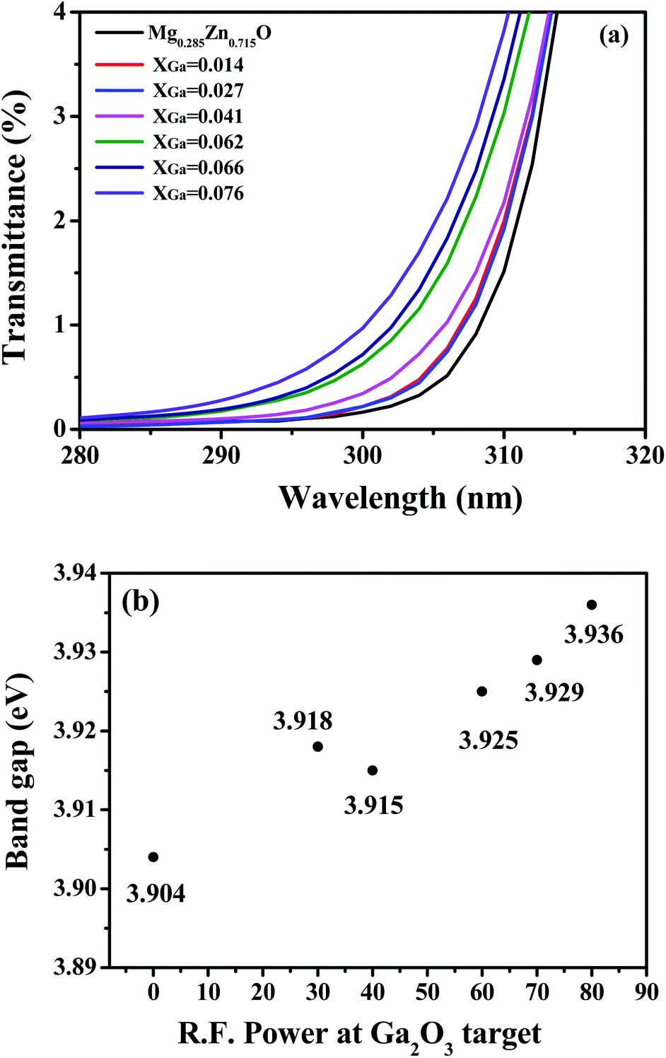 | ||
| Fig. 3 (a) Transmittance spectra and (b) bandgap energies of the Mg0.28Zn0.72O and various MgZnO:Ga thin films. | ||
 | ||
| Fig. 4 Piezoresponse force microscopy results of the piezoelectric coefficient of the MgZnO:Ga thin films with Ga concentration. | ||
Fig. 5 shows the stress sensing properties of the pressure sensor incorporating various MgZnO:Ga thin films through current–voltage (I–V) characteristics with/without the application of stress (Table S3†). All I–V curves (Fig. 5a–c) demonstrated a typical Schottky diode behavior, except for noticeable leakage current found in the MgZnO (XGa = 0)-based device, probably originating from smaller SBH, as evidenced by the trend of the larger turn-on voltage with Ga doping. Nevertheless, high conductivity accompanied by Ga doping can be observed in the current reading under no stress condition, where the current gradually increases from 0.698 mA at 5 V for the undoped MgZnO film to 0.857 mA (XGa = 0.027), 2.519 mA (XGa = 0.041) with the increase in the Ga concentration. The piezotronic response is distinct for all devices, in that the applied compressive stress renders the SBH to decrease and the current to increase, where the current change is acquired as 0.698 mA to 0.828 mA for MgZnO, 0.857 mA to 1.032 mA for XGa = 0.027, and 2.519 mA to 2.939 mA for XGa = 0.041.
 | ||
| Fig. 5 Unstressed and stressed (0.2 kgf) I–V characteristics of the piezotronic stress sensors made of MgZnO:Ga films: (a) XGa = 0 (Mg0.28Zn0.72O) (b) XGa = 0.027 and (c) XGa = 0.041, with the corresponding (d) SBH change, (e) sensitivity of change in current and (f) stress sensitivity. | ||
Through the thermionic emission theory, the change in the SBH (ΔΦb) due to the applied stress can be calculated from  , where I(ε) and I(0) refer to the current reading under stress and no-stress, respectively. ΔΦb in Fig. 5d increased initially with the Ga doping from −4.41 meV (MgZnO) to −4.81 meV (XGa = 0.027), and decreased to −3.99 meV at high a Ga doping concentration (XGa = 0.041). Besides, the sensitivity of change in current at 0.2 kgf (Fig. 5e), defined as
  was enhanced from 0.186 for the pristine MgZnO to 0.204 (XGa = 0.027), which decreased to 0.166 at XGa = 0.041. The stress sensitivity (Fig. 5f, Table S4†), as defined by
  , increased from 28.50 MPa−1 (XGa = 0) to 31.36 MPa−1 (XGa = 0.027) and decreased to 25.56 MPa−1 (XGa = 0.027) with Ga doping, indicating the synergistic effects of Ga doping and Mg alloying over the pressure sensing performance of Ga-doped MgZnO films. In general, Ga doping leads to the generation of more free electrons in MgZnO, which in turn induces higher screening effects to adversely affect the piezopotential. The trend in the enhancement of the piezotronic pressure sensor with Ga doping was consistent with the trend in d33 value in Fig. 4. Moreover, more force-dependent I–V curves (Fig. 6a, Table S5†) for stress sensitivity were obtained for the device with 1.77 at% of Ga (XGa = 0.041)-doped MgZnO thin film showing linear increase in the ΔΦb (Fig. 6b) and linear increase in the sensitivity (Fig. 6c) with an increase in the external force (0, 0.2 and 0.5 kg). The corresponding stress sensitivity (Fig. 6d) was relatively high (31 ± 2 MPa−1) at low force (≦0.5 kg). The stress sensitivity (∼1.03 × 10⁻³ gf−1, 31 ± 2 MPa−1 @ 3 V) was comparatively low as compared to the earlier publisehd reports on ZnO nanowire array (4.7 × 10⁻² gf−1) and the MgO layer-coated ZnO nanowire array (∼104).16 However, it was unreasonable to make a direct comparison due to the significantly higher thickness of the ZnO nanowire array (∼4 μm) as compared to the Ga:MgZnO pressure sensor (500 nm), large difference in the device design and lack of literature related to the thin film-based piezotronic pressure sensor devices. In comparison with the non-piezotronic pressure sensors such as ultrathin Au nanowires9 (>1.14 kPa−1) or flower-like SnSe2 nanoplates10 (433.22 kPa−1), the stress sensitivity of the Ga:MgZnO pressure sensor was low (∼0.03 kPa−1). However, the sensor device size, design, fabrication process and dimension of Au nanowires and SnSe2 nanoplates were completely different to make any valid comparison with thin film-based pressure sensors. Moreover, the minimum pressure for the sensor to detect the change in current was ∼312 Pa (Fig. S5†), and the sensor was relatively stable under the application and release of stress for several cycles (Fig. S6†). The present investigation validates the combined effects of Ga doping and Mg alloying over the variation in the piezopotential, which led to a significant enhancement in the stress sensitivity of the MgZnO:Ga thin film pressure sensor. Furthermore, this unique approach could be extended using other suitable dopants to boost the pressure sensing performance of MgZnO thin films.
 | ||
| Fig. 6 (a) I–V characteristics, (b) SBH change, (c) sensitivity of the change in current and (d) stress sensitivity of the piezotronic stress sensor made of an MgZnO:Ga (XGa = 0.041) thin film under various external forces (0.2 kg and 0.5 kg). | ||
4. Conclusions
In summary, strong c-axis-oriented, high crystalline MgZnO:Ga thin films with various Ga compositions were fabricated on p-type Si (111) substrates, and the pressure sensing performance was investigated. The combined effect of Ga doping and Mg alloying led to the large enhancement of the piezopotential and subsequently the stress sensitivity of the MgZnO piezotronic pressure sensor at the optimum Ga doping concentration. XRD results described that all films had a (0002) preferential orientation with a nanorod-like columnar morphology, as investigated by SEM. Slow scan XRD results revealed that the peaks shifted depending on the amount of XGa and XMg in the films. Piezoresponse force microscopy results revealed that the MgZnO:Ga thin films with intermediate Ga concentration (XGa = 0.027) could achieve a higher piezoelectric coefficient (d33) = 33.17 pm V−1.Conflicts of interest
There are no conflicts to declare.Acknowledgements
This work was financially supported by the Hierarchical Green-Energy Materials (Hi-GEM) Research Center, from The Featured Areas Research Center Program within the framework of the Higher Education Sprout Project by the Ministry of Education (MOE) and the Ministry of Science and Technology (MOST 110-2634-F-006 -017) in Taiwan.References
- J. Zhou, Y. Gu, P. Fei, W. Mai, Y. Gao, R. Yang, G. Bao and Z. L. Wang, Nano Lett., 2008, 8, 3035–3040 CrossRef CAS PubMed.
- M. Amjadi, A. Pichitpajongkit, S. Lee, S. Ryu and I. Park, ACS Nano, 2014, 8, 5154–5163 CrossRef CAS PubMed.
- X. Xiao, L. Yuan, J. Zhong, T. Ding, Y. Liu, Z. Cai, Y. Rong, H. Han, J. Zhou and Z. L. Wang, Adv. Mater., 2011, 23, 5440–5444 CrossRef CAS.
- Z. Zhang, Q. Liao, X. Zhang, G. Zhang, P. Li, S. Lu, S. Liu and Y. Zhang, Nanoscale, 2015, 7, 1796–1801 RSC.
- Z. L. Wang, Nano Today, 2010, 5, 540–552 CrossRef CAS.
- Y. Hu, Y. Chang, P. Fei, R. L. Snyder and Z. L. Wang, ACS Nano, 2010, 4, 1234–1240 CrossRef CAS.
- Z. Zhang, Q. Liao, X. Yan, Z. L. Wang, W. Wang, X. Sun, P. Lin, Y. Huang and Y. Zhang, Nano Res., 2014, 7, 190–198 CrossRef CAS.
- Q. Liao, M. Mohr, X. Zhang, Z. Zhang, Y. Zhang and H.-J. Fecht, Nanoscale, 2013, 5, 12350–12355 RSC.
- S. Gong, W. Schwalb, Y. Wang, Y. Chen, Y. Tang, J. Si, B. Shirinzadeh and W. Cheng, Nat. Commun., 2014, 5, 1–8 Search PubMed.
- W. Li, K. He, D. Zhang, N. Li, Y. Hou, G. Cheng, W. Li, F. Sui, Y. Dai and H. Luo, ACS Appl. Energy Mater., 2019, 2, 2803–2809 CrossRef CAS.
- W. Li, L. Xiong, N. Li, S. Pang, G. Xu, C. Yi, Z. Wang, G. Gu, K. Li and W. Li, J. Mater. Chem. C, 2019, 7, 10179–10186 RSC.
- M. Chen, J. Xia, J. Zhou, Q. Zeng, K. Li, K. Fujisawa, W. Fu, T. Zhang, J. Zhang and Z. Wang, ACS Nano, 2017, 11, 9191–9199 CrossRef CAS PubMed.
- K. He, Y. Hou, C. Yi, N. Li, F. Sui, B. Yang, G. Gu, W. Li, Z. Wang and Y. Li, Nano Energy, 2020, 73, 104743 CrossRef CAS.
- M. Chen, Z. Wang, X. Ge, Z. Wang, K. Fujisawa, J. Xia, Q. Zeng, K. Li, T. Zhang and Q. Zhang, Matter, 2020, 2, 666–679 CrossRef.
- S. Lu, J. Qi, Z. Wang, P. Lin, S. Liu and Y. Zhang, RSC Adv., 2013, 3, 19375–19379 RSC.
- X. Liao, X. Yan, P. Lin, S. Lu, Y. Tian and Y. Zhang, ACS Appl. Mater. Interfaces, 2015, 7, 1602–1607 CrossRef CAS.
- S. Major, A. Banerjee and K. Chopra, Thin Solid Films, 1983, 108, 333–340 CrossRef CAS.
- H. Agura, A. Suzuki, T. Matsushita, T. Aoki and M. Okuda, Thin Solid Films, 2003, 445, 263–267 CrossRef CAS.
- V. Bhosle, A. Tiwari and J. Narayan, J. Appl. Phys., 2006, 100, 033713 CrossRef.
- T. Makino, Y. Segawa, M. Kawasaki, A. Ohtomo, R. Shiroki, K. Tamura, T. Yasuda and H. Koinuma, Appl. Phys. Lett., 2001, 78, 1237–1239 CrossRef CAS.
- L. Kukreja, S. Barik and P. Misra, J. Cryst. Growth, 2004, 268, 531–535 CrossRef CAS.
- Y. Yang, C. Song, X. Wang, F. Zeng and F. Pan, J. Appl. Phys., 2008, 103, 074107 CrossRef.
- J. Luo, Y. Yang, X. Zhu, G. Chen, F. Zeng and F. Pan, Phys. Rev. B: Condens. Matter Mater. Phys., 2010, 82, 014116 CrossRef.
- Y. Yang, C. Song, X. Wang, F. Zeng and F. Pan, Appl. Phys. Lett., 2008, 92, 012907 CrossRef.
- N. Sinha, S. Goel, A. J. Joseph, H. Yadav, K. Batra, M. K. Gupta and B. Kumar, Ceram. Int., 2018, 44(7), 8582–8590 CrossRef CAS.
- L. Kumari, W. Li, C. H. Vannoy, R. M. Leblanc and D. Wang, Ceram. Int., 2009, 35, 3355–3364 CrossRef CAS.
- Y. J. Chen, S. Brahma, C. P. Liu and J.-L. Huang, J. Alloys Compd., 2017, 728, 1248–1253 CrossRef CAS.
- J.-S. Shiau, S. Brahma, J.-L. Huang and C.-P. Liu, Appl. Mater. Today, 2020, 20, 100705 CrossRef.
- S. W. Shin, I. Y. Kim, G. V. Kishor, Y. Y. Yoo, Y. B. Kim, J. Y. Heo, G.-S. Heo, P. S. Patil, J. H. Kim and J. Y. Lee, J. Alloys Compd., 2014, 585, 608–613 CrossRef CAS.
- I. Y. Kim, K. Gurav, S. W. Shin, K. S. Jeon, P. Patil, J. H. Moon, D. S. Lee and J. H. Kim, Sci. Adv. Mater., 2016, 8, 610–617 CrossRef CAS.
- S.-H. Jeong, J.-H. Park and B.-T. Lee, J. Alloys Compd., 2014, 617, 52–57 CrossRef CAS.
- Dhananjay and S. Krupanidhi, Appl. Phys. Lett., 2006, 89, 082905 CrossRef.
- C. Hinkle, A. Sonnet, E. Vogel, S. McDonnell, G. Hughes, M. Milojevic, B. Lee, F. Aguirre-Tostado, K. Choi and H. Kim, Appl. Phys. Lett., 2008, 92, 071901 CrossRef.
- R. Kara, L. Mentar and A. Azizi, RSC Adv., 2020, 10, 40467–40479 RSC.
- M. Ajili, M. Castagné and N. K. Turki, Superlattices Microstruct., 2013, 53, 213–222 CrossRef CAS.
- X. Wang, C. Song, D. Li, K. Geng, F. Zeng and F. Pan, Appl. Surf. Sci., 2006, 253, 1639–1643 CrossRef CAS.
- Ü. Özgür, Y. I. Alivov, C. Liu, A. Teke, M. Reshchikov, S. Doğan, V. Avrutin, S.-J. Cho and H. Morkoc, J. Appl. Phys., 2005, 98, 11 CrossRef.
Footnotes |
| † Electronic supplementary information (ESI) available. See DOI: 10.1039/d0na01069c |
| ‡ These authors (Sanjaya Brahma, Ping Han Lee) have equal author contributions. |
| This journal is © The Royal Society of Chemistry 2021 |