
 Open Access Article
 This Open Access Article is licensed under a Creative Commons Attribution-Non Commercial 3.0 Unported Licence
Pressure dependent conduction of individual multi-walled carbon nanotubes: the effect of mechanical distortions†
Chris J.
Barnett
a,
Cathren E.
Gowenlock
a,
Alvin
Orbaek White
 a and
Andrew R.
Barron
*abc
a and
Andrew R.
Barron
*abc
aEnergy Safety Research Institute, Swansea University, Bay Campus, Swansea, SA1 8EN, Wales, UK. E-mail: a.r.barron@swansea.ac.uk
bDepartment of Chemistry, Department of Materials Science and Nanoengineering, Rice University, Houston, Texas 77007, USA
cFaculty of Engineering, Universiti Teknologi Brunei, Jalan Tungku Link, Gadong, BE1410, Brunei Darussalam
First published on 2nd January 2021
Abstract
Multi-walled carbon nanotubes (MWCNTs) show an oscillation in electrical resistance (from I–V measurements) during mechanical distortion in which peak separation is inversely correlated with the diameter of the MWCNTs. These results provide the first experimental support of the theoretical prediction that distortion causes Van Hove singularities and Dirac cones in MWCNTs to misalign and cause the opening of the band gap, and suggest that when fabricating contacts for CNTs for device applications, the pressure caused by the contact deposition method must be taken into account for manufacturing devices with consistent properties.
Since the discovery of carbon nanotubes (CNTs) there has been much research into their uses in devices such as transistors1–3 and sensors.4,5 However, during the fabrication of such devices CNTs can undergo stress and strain, which can cause deformation of the nanostructure, the effects of which can be employed as the detection mode for sensors,6,7 and as a consequence there have been a number of theoretical modelling studies that predict that deformation caused by either pressure or bending of CNTs will open the band gap of tubes with zig-zag chirality.8–10 Yang and Han explained that the opening of the band gap, in simulation, is caused by the Fermi point moving across allowed electronic states due to shifts, merges and splits of Van Hove singularities (VHS).11 However, there is no experimental verification of such an effect. We have recently demonstrated the use of in situ electrical measurements on individual multi-walled carbon nanotubes (MWCNTs),12 which enables the conformation of theoretical predictions of the angular and overlap dependence of conduction between two identical CNTs.13 Herein, we have employed these methods to experimentally investigate the effects of exerting pressure to cause deformation of MWCNTs on electrical conduction; furthermore, measurements on multiple samples provide insight into the effect on different diameter MWCNTs.
MWCNTs were synthesised using a table top horizontal tube reactor,14 and subjected to microwave irradiation followed by chlorine treatment to remove the majority of the residual iron catalyst.15 For safety, dry MWCNTs were handled as previously reported.16 The MWCNTs were suspend in ethanol, sonicated and drop cast onto Si wafer with a native oxide. The sample was loaded into an Omicron LT Nanoprobe (base pressure 10−10 mbar) and argon was bombarded using a PSP ISIS 3000 ion gun at 0.3 keV to remove surface contamination and ensure consistent contacts.12 The Raman spectrum of the MWCNTs is shown in Fig. S1 (see the ESI).†
Nanoscale 2-point-probe (2PP) measurements were carried out using etched tungsten probes that have been direct current annealed to remove the shank oxide,17,18 and approached onto isolated MWCNTs (Fig. 1a) using previously described methods to ensure minimal strain.19 Nanoscale 2 point probe IV measurements were carried out by sweeping the voltage from −1 V to 1 V, with a probe separation of 5 μm. After the initial I–V sweep one of the probes was approached in steps of 1 nm (measured as the extension of the piezo that controls the tip), up to a maximum of 15 nm, into the nanotube and after each step the I–V measurement was re-taken. A similar procedure was used to withdraw the tip. It should be noted that due to the unknown contact area and elastic properties of the tip and CNTs it is not possible to reliably calculate the force exerted. The SEM images in Fig. 1 show tip positions that are used to measure the diameter of the CNTs but the resolution of SEM is far below that needed to observe distortion induced in the CNTs.
 | ||
| Fig. 1 SEM images of (a) 2 tungsten probes on an isolated MWCNT and (b) 3 tungsten probes on an isolated MWCNT with the centre probe floating. | ||
To understand if any changes observed were due to distortion induced strain of the MWCNTs or improved contact due to pressure exerted by the tip, nanoscale 2PP measurements were carried out on 3 other isolated MWCNTs with a third floating probe (so current would not be drawn) positioned in the middle of the outer voltage probes and used to induced strain through distortion, as shown in Fig. 1b. To ensure that the strain induced by the floating probe did not affect the contacts under the outer probes, the maximum displacement was 10 nm and the outer probe was separated by 3–5 μm. 3PP measurements were carried out on three MWCNTs with diameters 100 nm, 120 nm and 140 nm and the probe separations were 4.2 μm, 4.9 μm and 3.7 μm, respectively.
From the nanoscale 2PP I–V measurements it was determined that the MWCNT had a measured resistance of 5.8 kΩ and pressing the tip into the tube caused the resistance to decrease to 5.6 kΩ (blue circle data points in Fig. 2). It can be seen that the resistance drops significantly over the first 8 nm of depression, measured as the extension of the piezo that controlled the tip; further depression did not significantly reduce the resistance; however, there is an oscillation in the final 7 points of depression.
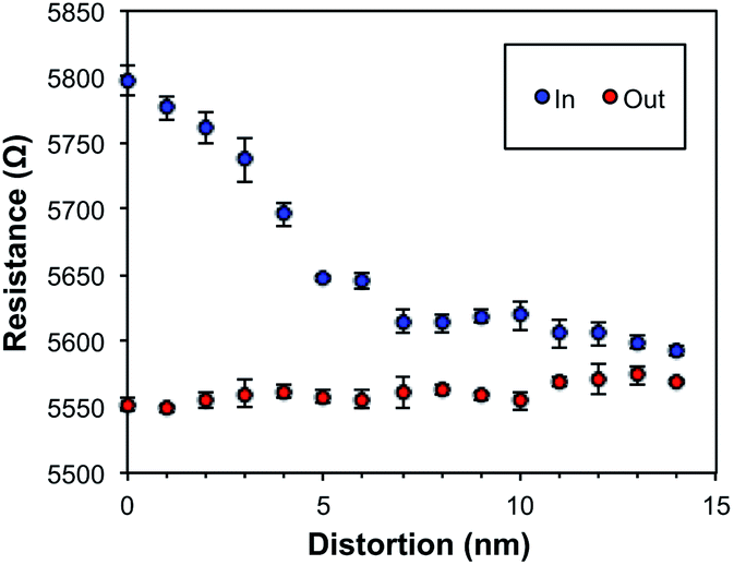 | ||
| Fig. 2 Plot of the electrical resistance of an individual MWCNT as determined from 2PP I–V measurements as a function of distortion induced by pressure applied by one of the probes (measured as the extension of the piezo that controls the tip). The blue circle data points show the values with the depression of the probe and the red circle data points show the resistance upon relaxation of distortion by removal of the probe (error bars show the standard error). | ||
Withdrawing the tip resulted in no significant change in resistance when compared to the resistance measured at maximum depression (see red circle data points in Fig. 2). However, there is an oscillation similar to that seen when depressing the tube from 7–14 nm. We attribute the initial decrease in resistance when the tip is pushed into the sample to an improved contact interface either due to the tip pushing through surface contamination remaining after argon bombardment or due to the nanotube's surface deforming around the tip increasing the contact area.12
There are a number of possible reasons for the observed oscillation (see below); however, to ensure this is not a result of contact changes due to distortion, a third, electrically floated tip was brought into contact between the two probes that applied a voltage to the isolated nanotube (Fig. 1b). The electrically floated tip was used to distort the centre of the tube and I–V measurements were performed during depression and relaxation. As the nanotube is depressed the resistance increases (Fig. 3); however, since the outer probes are not moved there will be no changes in the contacts due to any remaining surface contamination; therefore, this is attributed to the increased strain.11 This trend is in agreement with the 2PP measurements (see red data points in Fig. 2). From Fig. 3 it can also be seen that oscillation is also present in the 2PP measurements and is highlighted using the red line in Fig. 3. The equation for the red line is give in the ESI† and is a simple fit aimed to help the reader's eye and not an exact match of the system. As the middle probe is withdrawn the resistance reduces back to its original value (Fig. S2, see the ESI†).
 | ||
| Fig. 3 Plot of the electrical resistance of an individual MWCNT as determined from 3PP I–V measurements as a function of distortion, induced by pressure applied by the central “floating” probe, distortion (measured as the extension of the piezo that controls the tip) (black line) and calculated fit (red line) highlighting the oscillations. | ||
Repeated distortion and relaxation of the MWCNT by the central probe causes no hysteresis in the resistance curves indicating no permanent change in the electrical properties of the MWCNTs (Fig. S1, see the ESI†). For repeat measurements the floating probe was withdrawn out of contact with the CNTs and replaced for the measurements; therefore due to electrostatic interactions between the tip and the CNTs, the tip and the nanotube can shift relative to each other, resulting in an offset in the oscillations. Analysis of the I–V curves from adjacent peaks and troughs shows that the I–V curves obtained from the resistance peaks are more rectifying in nature than those obtained in the troughs of resistance. Fig. 4 shows typical normalised I–V curves obtained from adjacent resistance peaks (black line) and troughs (red line) which shows that at a resistance peak, the contact between the MWCNT and the tungsten probe in more rectifying, i.e., the MWCNT oscillates from being more metallic to more semiconducting as distortion is applied.
 | ||
| Fig. 4 Normalised I–V curves of a typical resistance peak (black line) and adjacent resistance tough (red line) in the oscillations observed for the electrical resistance of an individual MWCNT determined from 3PP I–V measurements caused by distortion induced by pressure applied by a central “floating” probe, shown in Fig. 3. | ||
To determine if the observed oscillation was CNT dependent, the procedure described above was carried out on 3 different MWCNTs with different diameters and all showed the same trend as seen in Fig. 3. However, Fast Fourier Transform (FFT) analysis of the distance between peaks in the oscillation of resistance (i.e., the frequency of oscillation) shows that peak separation decreases with increased nanotube diameter, as shown in Fig. 5. Examples of the FFT are shown in Fig. S3 (see the ESI).†
 | ||
| Fig. 5 Plot of peak separation in the oscillations observed for the electrical resistance of an individual MWCNT (determined from 3PP I–V measurements caused by distortion induced by pressure applied by a central “floating” probe) as a function of the MWCNT diameter. | ||
There are several possibilities for the observed oscillation of resistance with depression and relaxation. It could be caused by changes in contact resistance between the current–voltage probes and the CNTs; however, these probes are not moved during the experiment and placed at a distance considerably greater than the distortion away from the third floating probe meaning contact changes are highly unlikely. The nanotubes have also been argon bombarded to remove surface contamination to ensure consistent contacts.12 The oscillation could be caused by alignment of the carbon rings in adjacent shells within the MWCNT.13 It has been shown that when the carbon rings in parallel CNTs or graphene sheets are in registry the conductivity between the CNTs or sheets increases.13,20,21 However, we do not believe that this is reasonable, since peak separation of any variation would be independent of the nanotube diameter because the C–C distances are constant irrespective of the CNT diameter. Instead our experimental results are supportive of prior theoretical models.
Yang and Han predicted that for CNTs under pressure Van Hove singularities (VHS) shift in and out of alignment causing the band gap to open and close.11 Furthermore Raman experiments have shown that energy separation between VHS shifts with induced strain on CNTs.22,23 It should be noted that VHS are usually only considered in relation to single walled carbon nanotubes; however, recent publications on distorted graphene and twisted graphene have shown opening of Dirac cones, superlattice VHS formed by Dirac cones and shifts in VHS.24–26 On the scale that we have measured here, the surface of the MWCNTs could act as graphene or twisted graphene, and therefore, we attribute our experimental findings to the opening and closing of the band gap with distortion. As the band gap opens the contact type changes to more rectifying, as observed in Fig. 4. This would also explain the observed oscillation in resistance with distortion of the MWCNTs. Furthermore, as the nanotube diameter increases the VHS are more densely packed which causes the Fermi point to cross more frequently under distortion resulting in the decrease in peak separation for CNTs with large diameters (i.e., consistent with the results in Fig. 5).
In conclusion, I–V measurements have been carried out on individual MWCNTs while undergoing distortion, and increasing the pressure at the contact reduces overall electrical resistance but this does not increase as the pressure is released, suggesting that the effect is caused by the contact pushing through residual surface contamination.13 More importantly, we have made the first experimental observation that distortion of a MWCNT due to pressure, by the contact or a third interaction, results in an oscillation in the measured resistance with distortion. This appears to confirm theoretical models that such a change is caused by the opening and closing of the band gap as the VHS and Dirac cones shift in and out of alignment.11 Furthermore, as the MWCNT diameter increases the frequency of the oscillation decreases, which is consistent with the VHS being more densely packed for larger CNTs, which causes the Fermi point to cross more frequently by a particular distance for distortion. Based upon these results we caution that when fabricating contacts for CNTs for devices, the pressure caused by the contact deposition method must be taken into account to manufacture consistent devices.
Conflicts of interest
There are no conflicts to declare.Acknowledgements
Financial support was provided by the Office of Naval Research (N00014-15-2717), the Welsh Government Sêr Cymru Chair Programme, and the Robert A. Welch Foundation (C-0002). The Welsh Government is acknowledged for Sêr Cymru II Fellowships (C. E. G. and A. O. W.) partly funded by the European Regional Development Fund (ERDF). Dr S. N. Shirodkar (Rice University) is acknowledged for useful discussion.References
- S. Park, M. Vosguerichian and Z. Bao, Nanoscale, 2013, 5, 1727–1752 RSC.
- D. M. Sun, C. Liu, W. C. Ren and H. M. Cheng, Small, 2013, 9, 1188–1205 CrossRef CAS.
- J. L. Blackburn, A. J. Ferguson, C. Cho and J. C. Grunlan, Adv. Mater., 2018, 30, 1–35 Search PubMed.
- E. Llobet, Sens. Actuators, B, 2013, 179, 32–45 CrossRef CAS.
- Y. Che, H. Chen, H. Gui, J. Liu, B. Liu and C. Zhou, Semicond. Sci. Technol., 2014, 29, 073001 CrossRef.
- S. Ryu, P. Lee, J. B. Chou, R. Xu, R. Zhao, A. J. Hart and S.-G. Kim, ACS Nano, 2015, 9, 5929–5936 CrossRef CAS.
- D. Sickert, S. Taeger, I. Kühne, M. Mertig, W. Pompe and G. Eckstein, Phys. Status Solidi B, 2006, 243, 3542–3545 CrossRef CAS.
- A. Rochefort, D. R. Salahub and P. Avouris, Chem. Phys. Lett., 1998, 297, 45–50 CrossRef CAS.
- R. Heyd, A. Charlier and E. McRae, Phys. Rev. B: Condens. Matter Mater. Phys., 1997, 55, 6820–6824 CrossRef CAS.
- L. Yang, M. P. Anantram, J. Han and J. P. Lu, Phys. Rev. B: Condens. Matter Mater. Phys., 1999, 60, 13874 CrossRef CAS.
- L. Yang and J. Han, Phys. Rev. Lett., 2000, 85, 155–157 Search PubMed.
- C. J. Barnett, C. Gowenlock, K. Welsby, A. Orbaek White and A. R. Barron, Nano Lett., 2018, 18, 695–700 CrossRef CAS.
- C. J. Barnett, C. Evans, J. E. McCormack, C. E. Gowenlock, P. Dunstan, A. Orbaek White and A. R. Barron, Nano Lett., 2019, 19, 4861–4865 CrossRef CAS.
- A. W. Orbaek, N. Aggarwal and A. R. Barron, J. Mater. Chem. A, 2013, 1, 14122–14132 RSC.
- V. Gomez, S. Irusta, W. W. Adams, R. H. Hauge, C. W. Dunnill and A. R. Barron, RSC Adv., 2016, 6, 11895–11902 RSC.
- V. S. Gangoli, P. M. V. Raja, G. L. Esquenazi and A. R. Barron, SN Appl. Sci., 2019, 1, 644 CrossRef.
- R. J. Cobley, R. A. Brown, C. J. Barnett, T. G. G. Maffeis and M. W. Penny, Appl. Phys. Lett., 2013, 102, 3–7 CrossRef.
- C. J. Barnett, O. Kryvchenkova, L. S. J. Wilson, T. G. G. Maffeis, K. Kalna and R. J. Cobley, J. Appl. Phys., 2015, 117, 174306 CrossRef.
- N. A. Smith, A. M. Lord, J. E. Evans, C. J. Barnett, R. J. Cobley and S. P. Wilks, Semicond. Sci. Technol., 2015, 30, 065011 CrossRef.
- A. Buldum and J. P. Lu, Phys. Rev. B: Condens. Matter Mater. Phys., 2001, 63, 161403 CrossRef.
- S. Paulson, A. Helser, M. Buongiorno Nardelli, R. M. Taylor, M. Falvo, R. Superfine and S. Washburn, Science, 2000, 290, 1742–1744 CrossRef CAS.
- M. Lucas and R. J. Young, Phys. Rev. B: Condens. Matter Mater. Phys., 2004, 69, 085405 CrossRef.
- S. B. Cronin, A. K. Swan, M. S. Ünlü, B. B. Goldberg, M. S. Dresselhaus and M. Tinkham, Phys. Rev. B: Condens. Matter Mater. Phys., 2005, 72, 035425 CrossRef.
- D. Zhai and N. Sandler, Mod. Phys. Lett. B, 2019, 33, 1930001 CrossRef CAS.
- A. J. H. Jones, R. Muzzio, P. Majchrzak, S. Pakdel, D. Curcio, K. Volckaert, D. Biswas, J. Gobbo, S. Singh, J. T. Robinson, K. Watanabe, T. Taniguchi, T. K. Kim, C. Cacho, N. Lanata, J. A. Miwa, P. Hofmann, J. Katoch and S. Ulstrup, Adv. Mater., 2020, 32, 2001656 CrossRef CAS.
- V. H. Nguyen and P. Dollfus, 2D Mater., 2015, 2, 035005 CrossRef.
Footnote |
| † Electronic supplementary information (ESI) available: Plot of the electrical resistance of MWCNTs as a function of distortion; a plot of the FFT of the electrical resistance of MWCNTs under distortion. See DOI: 10.1039/d0na01021a |
| This journal is © The Royal Society of Chemistry 2021 |