DOI:
10.1039/D0NA00939C
(Paper)
Nanoscale Adv., 2021,
3, 3875-3880
Synthesis of two-dimensional phenylethylamine tin–lead halide perovskites with bandgap bending behavior†
Received
10th November 2020
, Accepted 4th May 2021
First published on 4th May 2021
Abstract
Recently, two-dimensional (2D) metal halide perovskite materials with wide application in perovskite-based solar cells have attracted significant attention. Among them, 2D mixed lead–tin perovskites have not been systematically explored. Herein, we synthesize a 2D phenethylammonium (PEA) tin–lead bromide perovskite, PEA2SnxPb1−xBr4, via a simple solution-phase approach without toxic reagents and high temperatures. By tuning the ratio of Sn and Pb, the UV-vis absorption spectra showed unique bandgap bending behaviors. DFT calculations indicate the key effects of spin–orbital coupling (SOC) without the interference of lattice distortion. Moreover, we provided the standard equation with a correction term to introduce the influence of SOC. These results not only provide a step forward towards the bandgap engineering of perovskites, but also help to expand the application of 2D perovskite materials.
Introduction
Organic metal halide perovskites have been reported to have unique optoelectronic properties, such as a high photoluminescence quantum yield (PLQY), tunable emission wavelength, narrow emission peak, low exciton binding energy, long carrier diffusion lengths, and high defect tolerance.1–8 All these characteristics enable their potential application in solar cells, solar concentrators, LEDs, etc.9–12 2D perovskites with ammonium ions as A-site ions have gained attention because of their improved performance.13–15 In the general structure of 2D organic metal halide perovskites, metal-halide octahedrons form inorganic layers and are separated by organic ions.16–18 The staggered structure constitutes a semiconductor/insulator multi-quantum-well system with completely different electronic and optical properties.19 In addition, an inert organic layer to water and oxygen could protect the inorganic layer from oxidation and hydrolysis to improve the stability.20–25 Owing to improved protection, 2D structures are blessed with attractive potential in fields such as LEDs and solar cells.11,13,26,27
At present, lead halide perovskite materials show excellent properties but have huge limitations due to the toxicity of Pb. To determine a solution, several Pb-free perovskites were devised to obtain low-toxicity and high-performance devices.28–31 Because of their similar properties, Sn is regarded as a good choice to take the place of Pb to meet the requirements of low toxicity for applications. Meanwhile, Sn-based perovskite devices exhibit ideal performance, exemplified by LEDs, photovoltaic materials, and solar cells.26,32,33 However, Sn-based perovskite materials are regarded as having low stability for the oxidation of Sn2+. Alloy perovskites with Sn and Pb as B-site anions could increase the stability and widen their application. Based on the tunable content, Sn–Pb halide perovskites exhibit interesting properties.34 For example, Ginger's group reported an all-inorganic Sn–Pb perovskite, CsPbxSn1−xI3, as an electron transport layer with a low bandgap of 1.34 eV, which raised the power conversion efficiency to over 7%.35 Fan and co-workers indicated a CsSnxPb1−xBr3 single crystal with promising application as a photoelectronic device via morphology, structure, electron property and optical measurements.36 Janssen's group mentioned an FA0.66MA0.34Pb1−xSnxI3-based solar cell with the highest PCE of 16.1% at 50% Sn content through the passivation of NH4SCN.37 Briefly, Sn–Pb perovskite materials exhibit similar properties in applications and achieve tunability, stability and photoelectricity. The ideal potential of Sn–Pb perovskites has been indicated in applications; however the value of their physical and chemical properties must be researched in detail.
For a deeper understanding of bandgap tuning, researchers have focused on the bandgap change of Sn–Pb perovskites. The bandgap value of the system expressed by A1−xBx (x means the percent of a specific component) would commonly fit the following relationship:
| | | Egap(A1−xBx) = (1 − x)Egap(A) + xEgap(B) − Ax(1 − x) | (1) |
where
Egap represents the bandgap energy,
x is the component constant, and
A denotes the bending parameter. With the B-site anion changing from Sn to Pb, the bandgap shows a bending and Fan's group ascribed this nonlinear process by density functional theory calculations to the antagonistic action between the spin orbital coupling (SOC) effect and structural distortion.
35,36,38–41 However, it should be noted that the transformation process of the component from CH
3NH
3SnI
3 to CH
3NH
3PbI
3 went along with the change in the phases (from
P4
mm to
I4
cm at
x > 0.5).
41 Additionally, lattice transformation influenced the band energy transformation. It is worthwhile to study the influence of the SOC effect on bandgap bending without disturbance from other factors.
Compared with aliphatic ammonium, such as butylammonium (BA) and octylammonium (OctA), phenethylammonium (PEA) exhibits a lower nonradiative recombination rate because of weaker nonadiabatic coupling between band-edge states than BA and OctA.33,42 The aromatic ring in PEA increases the structural rigidity of 2D perovskites for strong interlayer π–π stacking.43,44 Therefore, PEA-based perovskites would indicate outstanding application performance in previous studies. Mathers's group indicated that PEA2PbCl4 exhibited remarkable performance in white LEDs. The color rendering index reached 84, and high photostability showed ideal application in natural white-light LEDs.45 Ling's group reported PEA2PbBrxCl4−x (0 < x < 4) with a high PLQY that increased from 0.2% to 16.9%. PEA2PbBrxCl4−x-based LEDs showed a wide range of color temperatures from 4000 K to 7000 K and a high color rendering index reaching approximately 90.46 Haque's group mentioned that (PEA)2SnBrxI4−x showed a high luminance of 0.15 cd m−2 at 4.7 mA cm−2 and an efficacy of 0.029 cd A−1 at 3.6 V in LEDs.47 Chou's group reported PEA2SnBrxI4−x with a wide photoluminescence range from 550–640 nm, a high PLQY of 6.4% and high photostability.48 Therefore, PEA-based perovskite materials might possess huge potential in several application fields.
Herein, we synthesized PEA2SnxPb1−xBr4 and studied the bandgap bending behavior. The absorption spectra showed special bending of the bandgap along with a change of bandgaps with different Sn contents. XRD patterns indicated that the phases had no change from pure Sn to pure Pb, which indicated that nonstructural factors would act on the band energy transformation. DFT calculations showed the important influence of the SOC effect on bandgap bending. As a result, bandgap bending was from the coaction of the SOC effect and mismatch of energy levels. Detailed research in this work on the mechanism could benefit the tuning of 2D perovskites and develop more high-performance devices.
Results and discussion
Luminescence and absorption spectra analyses
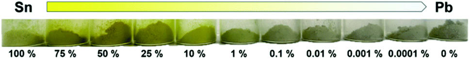
Photos of samples are shown in Fig. 1. Along with the decreasing content of Sn, the color changed from yellow (100% Sn) to white (0% Sn). UV-vis absorption spectra are shown in Fig. 2. Based on the absorption spectra, the absorption peaks of pure Sn and 75% Sn samples are located at 469 nm and 475 nm, respectively. This redshift indicated that the sample color changed to dark yellow. Then, the absorption peak shifted to blue so that the color of the powder changed to white. The blueshift was due to the smaller anion radius of Sn than Pb. The shift of the absorption peak indicated that the powder sample was not a mixture of several amounts of 2D PEA2SnBr4 and 2D PEA2PbBr4. In addition, emission properties were measured to study the influence of B-site content. The photoluminescence spectra shown in Fig. S3† were divided into two parts because the required excitation wavelengths were different. In perovskites, the 2D PEA2SnBr4 sample (100% Sn) showed weak photoluminescence at 477 nm under 450 nm laser excitation. Meanwhile, the 2D PEA2PbBr4 sample (0% Sn) showed stronger emission at approximately 420 nm under 365 nm laser excitation. The intensity peak of 2D PEA2SnBr4 was too low and too close to the excitation peak, which cannot be separated from the whole spectra. The main reason for weak photoluminescence is attributed to lattice defects. One-step synthesis decreased the time for sufficient crystal growth. In addition, an aqueous-phase Sn precursor might increase the possibility of oxidation of Sn (Sn2+ to Sn4+). These reasons might lead to lattice defects, which enhance nonradiative recombination in the energy transfer and relaxation process. In addition, the photoluminescence intensity decreased obviously with decreasing Sn content. When lower than 10%, the 477 nm peak almost disappears due to its poor emission intensity. Meanwhile, the 420 nm peak appeared and increased rapidly as the Sn content decreased. All emission properties were consistent with those in recent studies.46–48 Interestingly, only if the content of Sn was reduced to less than 1% could the emission of Pb be observed. This photoluminescence change process could be attributed to absorption properties. When the Sn content was lower than 1%, the absorption peak was located at approximately 412 nm. Compared with the required excitation wavelength of PEA2SnBr4, light over 412 nm could not be absorbed, and photoluminescence could not be excited. Additionally, the emission peak of Pb was located at approximately 420 nm. When the Sn content increased over 1%, the absorption band could cover the emission peak of Pb. As a result, the emission peak of Pb could be observed only when the content of Sn was less than 1%. In summary, the absorption spectra played a key role in the interesting optical properties as well as the special bending with increasing Sn content.
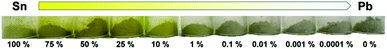 |
| | Fig. 1 Photos of Sn–Pb perovskites. From left to right, B-site cations changed from Sn to Pb. The Sn–Pb ratio of each sample is marked under the photos. | |
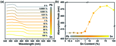 |
| | Fig. 2 (a) Absorption spectra of Sn–Pb bromide perovskites. Content percentage of Sn is marked above the line. (b) Absorption peak positions of different Sn content samples. In the two figures above, the B-site ingredient changed from total Sn to total Pb and was narrow from yellow to gray. | |
Structure and phase analyses
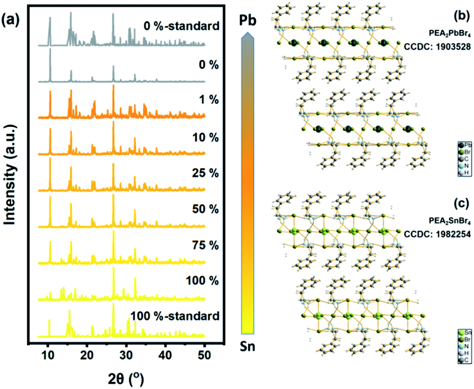
The structural influence of Sn content was measured via XRD patterns. All the results are shown in Fig. 3 and S2† (for details). Standard XRD patterns of PEA2SnBr4 and PEA2PbBr4 were based on previous studies from Sargent's group and Ma's group.26,49 Obviously, the introduction of Pb into the Sn host did not change the basic lattice. PEA2SnxPb1−xBr4 maintained the original P1 space group due to the similar ionic radii of Pb and Sn (rPb(II): 120 pm and rSn(II): 93 pm). The gap between the radii of Sn and Pb caused a few lattice contractions. However, the same valence and similar chemical properties determined the same coordination environment. Therefore, both Sn and Pb were surrounded by six bromide atoms and formed MBr64− (M = Sn/Pb) octahedrons. As a result, B-site anions could not influence the lattice structure. The key factor in bandgap bending should be the electronic structure.
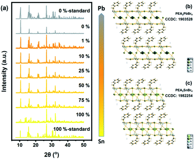 |
| | Fig. 3 (a) XRD patterns of Sn/Pb bromide perovskite. Standard patterns were single-crystal patterns from previous work. The B-site ingredient changed from total Sn to total Pb and was narrow from yellow to gray. (b) Crystal structure of PEA2SnBr4. (c) Crystal structure of PEA2PbBr4. | |
Previous work mentioned the Vegard law, namely, the linear shift process, which indicated a positive correlation between content and related properties such as photoluminescence and bandgap.47 This rule was reported in several systems, including II–VI quantum dots and perovskites.47,50,51 However, it was remarkable that the absorption spectra of PEA2SnxPb1−xBr4 had a distinctive shift different from common materials.52,53
Nevertheless, the bandgap change of PEA2SnxPb1−xBr4 exhibited special bending along with the content changes as shown in Fig. 2. Commonly, bandgap bending of semiconductors can be ascribed to the following reasons: (a) volume deformation potential effect, namely, the transformation of electronic structure from changes in volume, (b) chemical effects, namely, different atomic orbitals from different types of atoms at different energies, and (c) broken symmetry effect, namely, local relaxation and/or lattice distortions.54–56 Several recent studies attributed the bending of Sn–Pb perovskite to the combined reaction of spin–orbital coupling and lattice distortion. However, similar lattice constants and the same space group of Sn and Pb in PEA2SnxPb1−xBr4 indicate the impossibility of volume changes and symmetry breaking. The main difference is the atomic structure of Sn and Pb, which determined different energy band structures. It is the theoretical calculation that could research the relationship between the electric structure and content.
Theoretical calculation
Stevanović's work attributed the bandgap bending of CH3NH3SnxPb1−xBr3 hybrid perovskite to energy mismatches between the Pb-orbital and Sn-orbital.57 However, the coexistence of Pb and Sn would influence the electronic structure of the structure of the hybrid perovskite.36 Therefore, it was necessary to consider both electronic and chemical factors. To research the influence of the energy mismatch of the different atomic structures, atom and orbital projected densities of states for different ratios of Sn and Pb were calculated by density functional theory (DFT). Herein, we regarded four metal-bromide octahedrons with relative organic ammonium cations as a single unit and controlled the metal content to obtain different elemental ratios. Details are given in Scheme 1.
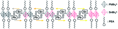 |
| | Scheme 1 Calculation unit in different element ratios. Black octahedra represent the PbBr6 unit, and red octahedra represent the SnBr6 unit. Hexagon with a wave line represent the PEA molecule. Each calculation unit contained four metal-bromide octahedra and all the relative PEA molecules. | |
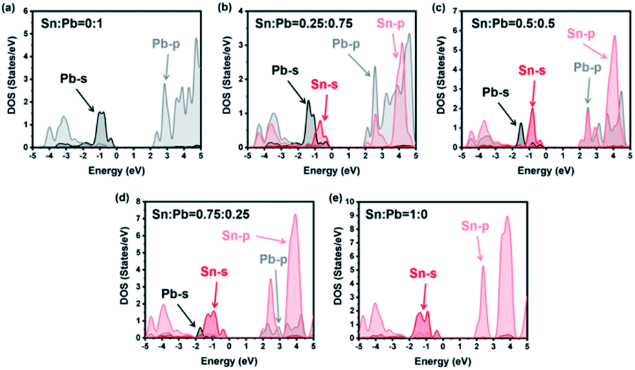
As shown in Fig. 4, the valence bands were formed by the mixture of the s atomic orbital from Sn or Pb and the p atomic orbital from Br. Meanwhile, the conduction bands were from the p–p interactions among the atoms. For instance, all the energy levels of Sn and Pb are listed in Table 1. The much higher bandgap of the 0% Sn sample should be attributed to the heavier mass of Pb than that of Sn, which agrees with previous studies.34,36,40,58–60 However, a special peak shift of the Pb-s orbital emerged when the Sn ratio was 0.25. As a result, the valence band maximum (VBM) changed from Pb-s/Br-p to Sn-s/Br-p, while the conduction band minimum (CBM) remained mainly Pb-p. Appropriately, the dominant position of Sn-p/Br-p was replaced by Pb-p/Br-p for CBM characters, while the VBM kept Sn-s as the main composition when the Sn ratio was 0.75. This phenomenon proved that the VBM and the CBM energy of the pure Sn structure were less than those of the pure Pb structure for the different energy levels of these two elements (see Table 1). However, SOC would enlarge the energy difference between Pb-p and Sn-p, especially in the poor-Sn structure.36,57 Then, the bandgaps of the structure further decreased, and special bending emerged in the process of the content changing from pure Sn to pure Pb.
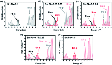 |
| | Fig. 4 Atom projected densities of states from calculation with SOC. Atomic ratios of Pb and Sn are marked at the top of each figure. Projections onto Pb-6s and Pb-6p are shown with black and gray lines, and Sn-5s and Sn-5p are shown with red and light-red lines. | |
Table 1 Relativistic atomic energy levels (eV)
|
|
s |
s1/2 |
p |
p1/2 |
p3/2 |
p–p1/2 |
| Sn |
−12.4 |
−12.3 |
−3.8 |
−4.9 |
−3.4 |
1.1 |
| Pb |
−10.9 |
−10.8 |
−4 |
−4.2 |
−3.8 |
0.3 |
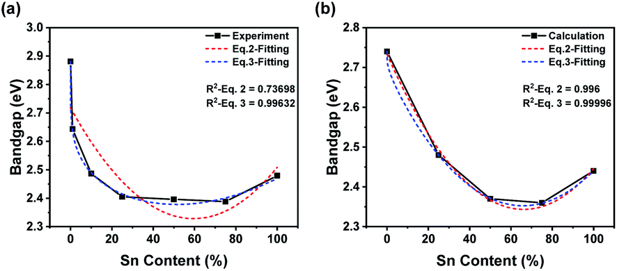
To research bandgap bending, we focused on the transformation of the bandgap. All raw data and fitting curves are shown in Fig. 5. Notably, the calculated results did not coincide with the experimental results (Fig. 5). The imperfect crystal we synthesized might be the key to the unexpected difference. In the calculation, we hypothesized that the crystal structures were perfect and that no lattice defects would appear. Moreover, the orders of calculated cells might be quite different from those of the synthesized sample. As a result, the calculated bandgap would be much lower than the experimental bandgap. In addition, the DOS-calculated results were much lower than the bandgap-calculated results because broadening of orbital peaks would benefit the DOS calculation (Fig. 5b). Therefore, the bandgap from DOS figures would be lower than the bandgap calculation. To study the relationship between bandgap bending and content transformation, we tried to fit the experimental and calculated results with a specific equation. Stevanovic's group mentioned a fitting equation (eqn (1)).57 We rewrote the equation into a simpler format (see eqn (2)).
| | | E(x) = (1 − x)E1 + xE2 − Ax(1 − x) | (2) |
E1 and
E2 are the bandgaps of the pure Pb structure and pure Sn structure, respectively, and
A is the bending constant. Fit curves are shown in
Fig. 5a. Obviously, the
R-squared values were too low, especially for the experimental curve, and the fitting results were not ideal. We hypothesized that the lack of corrections might be the reason for our unsatisfactory results. Previous studies mentioned that bandgap bending should result from a mismatch of energy levels and the SOC effect as well as lattice distortion.
57Eqn (2) utilized a linear term to describe the common progress of the bandgap and a nonlinear term to show the influence of other factors. The mismatch of energy levels was the core factor for bending, and the coaction between the SOC effect and lattice distortion was the core factor influencing the minimum bandgap.
36 For instance, antagonism between SOC and lattice distortion was observed. SOC would decrease the bandgap, which would be offset by lattice distortion. Moreover, the SOC effect exhibited a more prominent impact on the Pb-rich structure because of the heavy atom effect on Pb. Moreover, lattice distortion would also be aggravated in the Pb-rich structure compared with the pure Sn structure. However, in fact, no lattice distortion is considered in PEA
2Sn
xPb
1−xBr
4. Thus, the bandgap decrease of the Pb-rich structure should be larger than that of the Sn-rich structure. However,
eqn (2) (also
eqn (1)) could not show the different impacts on different Sn contents because the quadratic term reflected the minimum when the value of
x was 0.5. It was necessary to introduce a correction factor related to the Sn content to fix the deviation from the low effect in the Sn-poor structure. After several attempts, we introduced a correction factor into
eqn (2) as shown in
eqn (3).
| | | E(x) = (1 − x)E1 + x(E2 − B) − Ax(1 − x) + Bx0.2 | (3) |
E1 and
E2 are the bandgap of the pure Pb structure and pure Sn structure.
A was used to exhibit the bending constant from the mismatch of energy levels.
B was used to describe the SOC effect at different ratios of Sn and Pb. Fitting curves according to
eqn (3) are shown in
Fig. 5b. The exponent of the correction term was calculated from 0.01 to 1, and an exponent of 0.2 was chosen for the most ideal fitting degree (Fig. S1
†). It was apparent that the
R-squared values were close to 1, and much more ideal fitting results were obtained. Obviously, the SOC effect would reduce the bandgap of the Pb-rich structure much more than that of the Sn-rich structure. However, tremendous differences between the experimental and calculated curves should be noted. This difference could also be attributed to the low quality of the samples we synthesized. The disordered unit-cell arrangement of powder might cause an uneven sample, which would be quite different from the perfect crystal we used in the calculation. Thus, the curve from the experiment indicated that, especially in Pb-rich structures, the influence of the mismatch of energy levels was much less, while that of the SOC effect was much greater. As a result, the introduction of a correction term based on the SOC effect would improve the fitting level to bandgap changing of PEA
2Sn
xPb
1−xBr
4 and benefit the understanding of the SOC effect as well as the electronic structure for the perovskite.
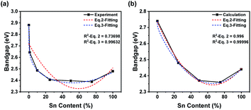 |
| | Fig. 5 Nonlinear fitting of lines from experimental data (a) and bandgap calculation (b). The differences were different fitting equations (red: eqn (2); blue: eqn (3)). Raw data are shown as black solid lines with symbols, and fitted curves are shown as colored dashed lines. Relative parameters are listed in each figure. | |
Conclusions
In summary, we demonstrated that the PEA-based Sn–Pb halide perovskite PEA2SnxPb1−xBr4 has excellent photoluminescence and absorption properties. The bandgap of PEA2SnxPb1−xBr4 showed special bending from PEA2PbBr4 to PEA2SnBr4. XRD patterns indicated an immovable lattice along with changes in B-site elements. DOS-based theoretical calculations indicated that the key reason for bandgap bending was coaction from the mismatch of energy levels and the SOC effect. Moreover, a correction term based on different influences stemming from Pb and Sn was introduced into the original bandgap bending equation to explain the effect of SOC without interference from lattice distortion. In addition, the anomalous changes in the bandgap presented the possibility to adjust the bandgap to a much lower value. The tunable bandgap shown in this work provides a new option for PEA2SnxPb1−xBr4 to be used in versatile optoelectrical fields.
Conflicts of interest
There are no conflicts to declare.
Acknowledgements
This research is supported by the Natural Science Foundation of China (22075129) and Natural Science Foundation of Jiangsu Province (Grant No. BZ2018008).
Notes and references
- F. Zhang, H. Zhong, C. Chen, X.-g. Wu, X. Hu, H. Huang, J. Han, B. Zou and Y. Dong, ACS Nano, 2015, 9, 4533–4542 CrossRef CAS PubMed.
- H. Huang, M. I. Bodnarchuk, S. V. Kershaw, M. V. Kovalenko and A. L. Rogach, ACS Energy Lett., 2017, 2, 2071–2083 CrossRef CAS PubMed.
- A. K. Guria, S. K. Dutta, S. D. Adhikari and N. Pradhan, ACS Energy Lett., 2017, 2, 1014–1021 CrossRef CAS.
- H. Huang, L. Polavarapu, J. A. Sichert, A. S. Susha, A. S. Urban and A. L. Rogach, NPG Asia Mater., 2016, 8, e328 CrossRef CAS.
- H. Wei, Y. Fang, P. Mulligan, W. Chuirazzi, H.-H. Fang, C. Wang, B. R. Ecker, Y. Gao, M. A. Loi, L. Cao and J. Huang, Nat. Photonics, 2016, 10, 333–339 CrossRef CAS.
- Z. Chen, Q. Dong, Y. Liu, C. Bao, Y. Fang, Y. Lin, S. Tang, Q. Wang, X. Xiao, Y. Bai, Y. Deng and J. Huang, Nat. Commun., 2017, 8, 1890 CrossRef PubMed.
- Z.-K. Wang, M. Li, Y.-G. Yang, Y. Hu, H. Ma, X.-Y. Gao and L.-S. Liao, Adv. Mater., 2016, 28, 6695–6703 CrossRef CAS PubMed.
- S. Sun, D. Yuan, Y. Xu, A. Wang and Z. Deng, ACS Nano, 2016, 10, 3648–3657 CrossRef CAS.
- G. H. Ahmed, J. K. El-Demellawi, J. Yin, J. Pan, D. B. Velusamy, M. N. Hedhili, E. Alarousu, O. M. Bakr, H. N. Alshareef and O. F. Mohammed, ACS Energy Lett., 2018, 3, 2301–2307 CrossRef CAS.
- J. Tong, J. Wu, W. Shen, Y. Zhang, Y. Liu, T. Zhang, S. Nie and Z. Deng, ACS Appl. Mater. Interfaces, 2019, 11, 9317–9325 CrossRef CAS PubMed.
- F. Cao, D. Yu, X. Xu, B. Cai, Y. Gu, Y. Dong, Y. Shen and H. Zeng, Small Methods, 2019, 3, 1900365 CrossRef CAS.
- S. Yuan, Z. K. Wang, M. P. Zhuo, Q. Tian, Y. Jin and L. S. Liao, ACS Nano, 2018, 12, 9541–9548 CrossRef CAS PubMed.
- L. N. Quan, Y. Zhao, F. P. García de Arquer, R. Sabatini, G. Walters, O. Voznyy, R. Comin, Y. Li, J. Z. Fan, H. Tan, J. Pan, M. Yuan, O. M. Bakr, Z. Lu, D. H. Kim and E. H. Sargent, Nano Lett., 2017, 17, 3701–3709 CrossRef CAS.
- Y. Ling, L. Tan, X. Wang, Y. Zhou, Y. Xin, B. Ma, K. Hanson and H. Gao, J. Phys. Chem. Lett., 2017, 8, 3266–3271 CrossRef CAS PubMed.
- L. Mao, Y. Wu, C. C. Stoumpos, M. R. Wasielewski and M. G. Kanatzidis, J. Am. Chem. Soc., 2017, 139, 5210–5215 CrossRef CAS PubMed.
- L. Dou, A. B. Wong, Y. Yu, M. Lai, N. Kornienko, S. W. Eaton, A. Fu, C. G. Bischak, J. Ma, T. Ding, N. S. Ginsberg, L.-W. Wang, A. P. Alivisatos and P. Yang, Science, 2015, 349, 1518 CrossRef CAS PubMed.
- D. B. Mitzi, Chem. Mater., 1996, 8, 791–800 CrossRef CAS.
- C. C. Stoumpos, D. H. Cao, D. J. Clark, J. Young, J. M. Rondinelli, J. I. Jang, J. T. Hupp and M. G. Kanatzidis, Chem. Mater., 2016, 28, 2852–2867 CrossRef CAS.
- R. Guo, Z. Zhu, A. Boulesbaa, F. Hao, A. Puretzky, K. Xiao, J. Bao, Y. Yao and W. Li, Small Methods, 2017, 1, 1700245 CrossRef.
- C. Zhou, H. Lin, H. Shi, Y. Tian, C. Pak, M. Shatruk, Y. Zhou, P. Djurovich, M.-H. Du and B. Ma, Angew. Chem., Int. Ed., 2018, 57, 1021–1024 CrossRef CAS PubMed.
- E. Jokar, C.-H. Chien, C.-M. Tsai, A. Fathi and E. W.-G. Diau, Adv. Mater., 2019, 31, 1804835 CrossRef PubMed.
- H. Huang, B. Pradhan, J. Hofkens, M. B. J. Roeffaers and J. A. Steele, ACS Energy Lett., 2020, 5, 1107–1123 CrossRef CAS.
- S. Seth, T. Ahmed, A. De and A. Samanta, ACS Energy Lett., 2019, 4, 1610–1618 CrossRef CAS.
- C. Zhou, H. Lin, Y. Tian, Z. Yuan, R. Clark, B. Chen, L. J. van de Burgt, J. C. Wang, Y. Zhou, K. Hanson, Q. J. Meisner, J. Neu, T. Besara, T. Siegrist, E. Lambers, P. Djurovich and B. Ma, Chem. Sci., 2018, 9, 586–593 RSC.
- C. Zhou, Y. Tian, M. Wang, A. Rose, T. Besara, N. K. Doyle, Z. Yuan, J. C. Wang, R. Clark, Y. Hu, T. Siegrist, S. Lin and B. Ma, Angew. Chem., Int. Ed., 2017, 56, 9018–9022 CrossRef CAS PubMed.
- L.-J. Xu, H. Lin, S. Lee, C. Zhou, M. Worku, M. Chaaban, Q. He, A. Plaviak, X. Lin, B. Chen, M.-H. Du and B. Ma, Chem. Mater., 2020, 32, 4692–4698 CrossRef CAS.
- Y. Hu, T. Qiu, F. Bai, W. Ruan and S. Zhang, Adv. Energy Mater., 2018, 8, 1703620 CrossRef.
- F. Hao, C. C. Stoumpos, D. H. Cao, R. P. H. Chang and M. G. Kanatzidis, Nat. Photonics, 2014, 8, 489–494 CrossRef CAS.
- P. C. Harikesh, H. K. Mulmudi, B. Ghosh, T. W. Goh, Y. T. Teng, K. Thirumal, M. Lockrey, K. Weber, T. M. Koh, S. Li, S. Mhaisalkar and N. Mathews, Chem. Mater., 2016, 28, 7496–7504 CrossRef CAS.
- Y. Kim, Z. Yang, A. Jain, O. Voznyy, G.-H. Kim, M. Liu, L. N. Quan, F. P. García de Arquer, R. Comin, J. Z. Fan and E. H. Sargent, Angew. Chem., Int. Ed., 2016, 55, 9586–9590 CrossRef CAS PubMed.
- P. Fu, M. Huang, Y. Shang, N. Yu, H.-L. Zhou, Y.-B. Zhang, S. Chen, J. Gong and Z. Ning, ACS Appl. Mater. Interfaces, 2018, 10, 34363–34369 CrossRef CAS PubMed.
- C. Zhou, Y. Tian, Z. Yuan, H. Lin, B. Chen, R. Clark, T. Dilbeck, Y. Zhou, J. Hurley, J. Neu, T. Besara, T. Siegrist, P. Djurovich and B. Ma, ACS Appl. Mater. Interfaces, 2017, 9, 44579–44583 CrossRef CAS PubMed.
- A. Wang, Y. Guo, Z. Zhou, X. Niu, Y. Wang, F. Muhammad, H. Li, T. Zhang, J. Wang, S. Nie and Z. Deng, Chem. Sci., 2019, 10, 4573–4579 RSC.
- T. Li, X. Chen, X. Wang, H. Lu, Y. Yan, M. C. Beard and D. B. Mitzi, ACS Energy Lett., 2020, 5, 347–352 CrossRef CAS.
- Z. Yang, X. Zhang, W. Yang, G. E. Eperon and D. S. Ginger, Chem. Mater., 2020, 32, 2782–2794 CrossRef CAS.
- Y. Xian, Y. Zhang, N. U. Rahman, H. Yin, Y. Long, P. Liu, W. Li and J. Fan, J. Phys. Chem. C, 2020, 124, 13434–13446 CrossRef CAS.
- J. Wang, K. Datta, J. Li, M. A. Verheijen, D. Zhang, M. M. Wienk and R. A. J. Janssen, Adv. Energy Mater., 2020, 10, 2000566 CrossRef CAS.
- F. Hao, C. C. Stoumpos, R. P. H. Chang and M. G. Kanatzidis, J. Am. Chem. Soc., 2014, 136, 8094–8099 CrossRef CAS PubMed.
- C. C. Stoumpos, C. D. Malliakas and M. G. Kanatzidis, Inorg. Chem., 2013, 52, 9019–9038 CrossRef CAS PubMed.
- H. Lu, C. Xiao, R. Song, T. Li, A. E. Maughan, A. Levin, R. Brunecky, J. J. Berry, D. B. Mitzi, V. Blum and M. C. Beard, J. Am. Chem. Soc., 2020, 142, 13030–13040 CrossRef CAS PubMed.
- J. Im, C. C. Stoumpos, H. Jin, A. J. Freeman and M. G. Kanatzidis, J. Phys. Chem. Lett., 2015, 6, 3503–3509 CrossRef CAS PubMed.
- D. Ghosh, A. J. Neukirch and S. Tretiak, J. Phys. Chem. Lett., 2020, 11, 2955–2964 CrossRef CAS PubMed.
- L. Mao, W. Ke, L. Pedesseau, Y. Wu, C. Katan, J. Even, M. R. Wasielewski, C. C. Stoumpos and M. G. Kanatzidis, J. Am. Chem. Soc., 2018, 140, 3775–3783 CrossRef CAS PubMed.
- N. Kawano, M. Koshimizu, Y. Sun, N. Yahaba, Y. Fujimoto, T. Yanagida and K. Asai, J. Phys. Chem. C, 2014, 118, 9101–9106 CrossRef CAS.
- K. Thirumal, W. K. Chong, W. Xie, R. Ganguly, S. K. Muduli, M. Sherburne, M. Asta, S. Mhaisalkar, T. C. Sum, H. S. Soo and N. Mathews, Chem. Mater., 2017, 29, 3947–3953 CrossRef CAS.
- S. Yang, Z. Lin, J. Wang, Y. Chen, Z. Liu, E. Yang, J. Zhang and Q. Ling, ACS Appl. Mater. Interfaces, 2018, 10, 15980–15987 CrossRef CAS PubMed.
- L. Lanzetta, J. M. Marin-Beloqui, I. Sanchez-Molina, D. Ding and S. A. Haque, ACS Energy Lett., 2017, 2, 1662–1668 CrossRef CAS.
- M.-Y. Chen, J.-T. Lin, C.-S. Hsu, C.-K. Chang, C.-W. Chiu, H. M. Chen and P.-T. Chou, Adv. Mater., 2018, 30, 1706592 CrossRef PubMed.
- X. Gong, O. Voznyy, A. Jain, W. Liu, R. Sabatini, Z. Piontkowski, G. Walters, G. Bappi, S. Nokhrin, O. Bushuyev, M. Yuan, R. Comin, D. McCamant, S. O. Kelley and E. H. Sargent, Nat. Mater., 2018, 17, 550–556 CrossRef CAS PubMed.
- A. V. G. Chizmeshya, M. R. Bauer and J. Kouvetakis, Chem. Mater., 2003, 15, 2511–2519 CrossRef CAS.
- W. Li, M. Pessa and J. Likonen, Appl. Phys. Lett., 2001, 78, 2864–2866 CrossRef CAS.
- T. C. Jellicoe, J. M. Richter, H. F. Glass, M. Tabachnyk, R. Brady, S. E. Dutton, A. Rao, R. H. Friend, D. Credgington, N. C. Greenham and M. L. Bohm, J. Am. Chem. Soc., 2016, 138, 2941–2944 CrossRef CAS PubMed.
- A. Mehta, J. Im, B. H. Kim, H. Min, R. Nie and S. I. Seok, ACS Nano, 2018, 12, 12129–12139 CrossRef CAS PubMed.
- S.-H. Wei and A. Zunger, Phys. Rev. B: Condens. Matter Mater. Phys., 1989, 39, 3279–3304 CrossRef CAS PubMed.
- T. Mattila, S.-H. Wei and A. Zunger, Phys. Rev. B: Condens. Matter Mater. Phys., 1999, 60, R11245–R11248 CrossRef CAS.
- C.-Y. Moon, S.-H. Wei, Y. Z. Zhu and G. D. Chen, Phys. Rev. B: Condens. Matter Mater. Phys., 2006, 74, 233202 CrossRef.
- A. Goyal, S. McKechnie, D. Pashov, W. Tumas, M. van Schilfgaarde and V. Stevanović, Chem. Mater., 2018, 30, 3920–3928 CrossRef CAS.
- R. J. Worhatch, H. Kim, I. P. Swainson, A. L. Yonkeu and S. J. L. Billinge, Chem. Mater., 2008, 20, 1272–1277 CrossRef CAS.
- P. Selvarajan, K. Kundu, C. I. Sathish, S. Umapathy and A. Vinu, J. Phys. Chem. C, 2020, 124, 9611–9621 CrossRef CAS.
- A. Karmakar, A. Bhattacharya, G. M. Bernard, A. Mar and V. K. Michaelis, ACS Mater. Lett., 2021, 3, 261–267 CrossRef CAS.
Footnote |
| † Electronic supplementary information (ESI) available. See DOI: 10.1039/d0na00939c |
|
| This journal is © The Royal Society of Chemistry 2021 |
Click here to see how this site uses Cookies. View our privacy policy here. 
 Open Access Article
 This Open Access Article is licensed under a Creative Commons Attribution-Non Commercial 3.0 Unported Licence
 a,
Jian
Zhou
a,
Jian
Zhou