
 Open Access Article
 This Open Access Article is licensed under a Creative Commons Attribution-Non Commercial 3.0 Unported Licence
Dynamic degradation of metallic nanowire networks under electrical stress: a comparison between experiments and simulations
Nicolas
Charvin
 a,
Joao
Resende
b,
Dorina T.
Papanastasiou
b,
David
Muñoz-Rojas
b,
Carmen
Jiménez
b,
Ali
Nourdine
a,
Daniel
Bellet
b and
Lionel
Flandin
*a
a,
Joao
Resende
b,
Dorina T.
Papanastasiou
b,
David
Muñoz-Rojas
b,
Carmen
Jiménez
b,
Ali
Nourdine
a,
Daniel
Bellet
b and
Lionel
Flandin
*a
aUniv. Grenoble Alpes, Univ. Savoie Mont Blanc, CNRS, Grenoble INP, LEPMI, 38000 Grenoble, France. E-mail: lionel.flandin@univ-smb.fr
bUniv. Grenoble Alpes, CNRS, Grenoble INP, LMGP, 38000 Grenoble, France
First published on 8th December 2020
Abstract
Metallic nanowire networks represent a promising solution for a new generation of transparent and flexible devices, including touch screens, solar cells and transparent heaters. They, however, lack stability under thermal and electrical stresses, often leading to the degradation of nanowires, which results in the loss of electrical percolation paths. We propose a comprehensive description of the degradation mechanism in a metallic nanowire network subjected to electrical stress. The nanowire network degradation is ascribed, at a very local scale, to the hot-spot formation and the subsequent propagation of a spatially correlated disruptive crack. We compare the behaviour of actual networks under electrical and thermal stresses to dynamic simulations of randomly deposited sticks on a 2D surface, and a thermal phenomenon simulated in a metal thin film. On one hand, such comparison allows us to deduce an average junction resistance between nanowires. On the other hand, we observed that initial flaws in a discrete network result in a local current density increase in the surrounding area, further leading to an amplified Joule effect. This phenomenon promotes the spatial correlation in the damage of the percolating network. Such non-reversible failure of the transparent electrode is in good agreement with experimental observations.
Introduction
The growing interest in flexible, efficient and low cost transparent electrodes has prompted the development of alternative solutions1,2 to transparent conductive oxides.3 In this matter, metallic nanowire networks exhibit outstanding properties, with sheet resistance values below 10 Ω sq−1, optical transparency of 90% and mechanical stability under repeated bending tests when deposited on flexible substrates.4,5 In particular, silver nanowire (AgNW) networks have been largely studied and already used as efficient transparent electrodes for solar cells,6 organic light emitting diodes,7 sensors,8 or as the main active material for transparent heaters (THs).9 AgNW networks possess several promising assets: the requirement of a small quantity of silver (∼0.1 g m−2), compatibility with low-cost solution-based deposition methods and excellent electrical and optical properties which can be combined with a unique flexibility.However, AgNW networks tend to degrade under electrical and thermal stresses, especially for the very demanding transparent heater applications but also for solar applications.10 The observed degradation, at the macroscopic scale, is described as a failure of the networks.11–14 For thermal instability, the degradation of the nanowires can be described as a fragmentation (or spheroidization) of the wires, described by the Plateau–Rayleigh instability: the associated driving force is the surface energy minimization of nanowires, causing the transformation into more spherical nanoparticles.10,13 Electromigration, which also has an effect on nanowire network transformation, can be defined as material migration caused by an electrical field.15 This phenomenon has many consequences in electrical interconnects in integrated circuits15 and has also been reported for AgNW networks.16,17 Nevertheless, electromigration will not be thoroughly considered in the present paper. Conversely to thermally induced instability which affects uniformly the whole specimen; during electrical breakdown, Sannicolo et al. showed that damage to the AgNW network is localized in a region called “network crack”, which spreads in a direction roughly parallel to opposite electrodes until reaching either sample edges.14 The sample has eventually lost its main conducting property. The crack propagation is time dependent and its growth can be directly tracked with an infrared (IR) camera.14
Successful simulations of metallic nanowire networks have been described with a random arrangement of linear sticks on a 2D surface.18–24 These models predict different macroscopic properties fairly well, such as optical transparency, percolation threshold and macroscopic resistance. Very few parameters are necessary to describe the challenging law of the percolation theory:13 the linear resistance of a single nanowire, and an estimation of the junction resistance between nanowires in contact. This kind of model has, up to now, been developed with static networks presenting different densities, essentially to compare with the well-known power law equation of the percolation theory.
The next step requires further understanding of the failure mechanisms and the potential consequences encountered during usage conditions for the different applications mentioned above. This requires the development of computation methods, and their calibration and thorough comparison with experimental results. The present work consists of enhancing models towards a time dependent simulation, including structural changes within the resistive network to mimic its progressive degradation under electrical stress. The proposed dynamic approach is based on the evaluation of the current distribution on a simulated network. A stepwise change in the microstructure of the network is then applied to account for the degradation of the most stressed links, at the AgNW scale. This allows a dynamic simulation of the alterations of the stressed network. The obtained local hot-spot formation and crack propagation, in agreement with experimental results, do induce a direct adjustment of the macroscopic resistance. Additionally, we simulated the thermal and electrical properties of a macroscopic system with a well-defined initial defect, using a thin metallic film as a model.
Experimental procedure and simulation description
Silver nanowire network deposition
AgNWs with an aspect ratio close to 100 (average diameter of 70 ± 10 nm and average length of 8 ± 3 μm) were kindly provided from the research team of Jean-Pierre Simonato from CEA-LITEN in Grenoble, France, being produced as detailed in Mayousse et al.25 Squared boroaluminosilicate Corning glass (1737) was used as a substrate, with a size of 25 × 25 mm2. Before AgNW deposition, the substrates were sonicated during 15 minutes in isopropanol, rinsed with distilled water, and finally dried with N2 gas. The deposition of the AgNW networks was conducted via spray-deposition using a home-made spray set-up composed of an airbrush (Harder & Steenbeck), a robotic arm and a heating plate. A suspension of AgNWs in methanol with a concentration of 0.1 g L−1 was used, and N2 was used as a spraying gas with a pressure of 1.4 bar. The substrates were heated at 110 °C to easily evaporate the solvent, and the density of the network was attained by controlling the number of spray cycles. 2 mm wide silver-paste electrodes were added on two opposite sides of the samples (by convention these contacts are vertical in all figures of the present article). Fig. 1a, b and c exhibit a picture, optical microscope image and SEM image, respectively, of a typical randomly deposited AgNW network, with a corresponding areal mass density (amd) of 93 mg m−2.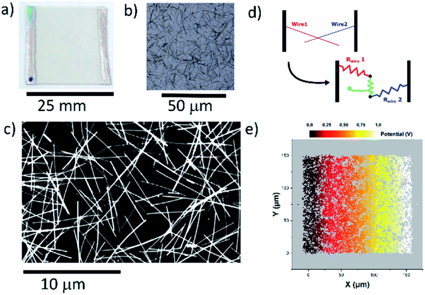 | ||
| Fig. 1 Deposited AgNW networks on glass and scheme of the computational simulation. (a) Picture of a 25 × 25 mm2 AgNW network on glass with electrodes on opposite edges. (b) Optical microscope image of the randomly deposited AgNW network. (c) SEM image of the AgNW network with nanowires of an average length of 8 μm and a diameter of 70 nm with a corresponding amd of 93 mg m−2. (d) Scheme of two intersecting nanowires, and how Rwire and Rcontact are considered in the simulation model. (e) Representation of a AgNW network (150 × 150 μm2) with a colour map representing the electrical potential under an applied voltage bias of 1 V between opposite vertical electrodes. | ||
Characterization techniques
The AgNW morphology was analysed by using an Optical Microscope (Leica DM LM) and with two Field Emission Gun-Scanning Electron Microscopes (FEG-SEM Environmental FEI QUANTA 250 and Zeiss GeminiSEM 300). The amd of the network was measured from 10 SEM images, using ImageJ software and the Skeletonize plugin.All electrical measurements were performed using a Keithley 2400 source-measure-unit (SMU), in a 4-wire configuration. A current sweep from 0.1 to 10 mA was initially performed to extract the sheet resistance of the sample, Rs, from a linear fit on the V(I) curve. All samples exhibited a perfectly ohmic behaviour under any circumstances. Then a degrading voltage ramp was applied at 1 V min−1 from 3 V up to the beginning of the breakdown. The SMU was then switched to constant-current mode, to perform continuous resistance measurements. For measuring electrical resistance the source level was set at 1 μA, to minimize the electrical stress on the sample resulting from the current flow itself. Meanwhile, an in situ IR imaging of the sample was performed, to record the temperature distribution on the sample area (from which the maximum temperature, Tmax, can be extracted), using a FLIR A320G IR camera placed above the setup. During all the electrical tests, the samples were held hanging in mid-air. The resulting heat-transfer processes could explain the wave-like temperature distribution along the X-direction, when one could expect a homogeneous distribution all over the sample.
Computational models
The Joule effect states that any electrical current flowing through a conductor induces heating. It has been shown that it is still valid for nanowires32 and it is currently used in transparent heaters based on metallic nanowires.9 We consider the degradation of a single AgNW at a microscopic level to be directly linked to the temperature of that particular wire. This temperature is directly dependent on the energy dissipated in the wire. An iterative damage phenomenon was thus simulated at a very individual and local scale by progressively and irreversibly modifying the nanowire network model, depending on the thermal destruction of single wires. The model only alters the percolation cluster, thanks to the underlying graph structure. Under a given voltage bias, the electrical current density j is determined in every resistor of the constructed graph (either Rwire or Rcontact type). At each iteration step, the resistor with the highest j, among all resistors whose j is larger than a defined threshold value jfailure, is selected. The corresponding resistor is then considered to be broken and removed from the graph. This process is repeated, until the network loses its percolating nature between the two opposite electrodes. The experimental critical current density jfailure can be derived from the observed voltage bias Vfailure at which failure occurs on a real sample.12 If the voltage bias is scaled according to the ratio (Lsx,simul/Lsx,exp), jfailure can be used as a realistic threshold in the simulation.
Results and discussion
The random deposition of AgNWs on a glass substrate results in transparent samples, as shown in Fig. 1a. Optical microscope images and SEM micrographs, represented respectively in Fig. 1b and c, show a network composed of AgNWs with an average nanowire length of 8 μm and a diameter of 70 nm with a corresponding amd of 93 mg m−2, and an initial macroscopic resistance of 8.9 Ω, similar to previous studies.30,31In order to compare with the deposited sample, the scheme of the numerically simulated nanowires is represented in Fig. 1d. Two different segments are represented with the additional contact resistance in-between. The density of the simulated network was that of the equivalent experimental sample (Dexp = 18.5 ± 0.9 in this case). The intrinsic linear AgNW resistance value was determined to be Rlin = 5.1 Ω μm−1. The contact resistance, also called junction resistance, was estimated by performing many simulations with the proposed model. Assuming the other parameters (sample dimensions, network density and intrinsic linear resistance of nanowires) are well-determined, simulations were run for varying Rc values. As shown in Fig. 2, Rs can then be represented as a linear function of Rc. Knowing the experimental sample sheet resistance, and expecting the simulated one to be the same, one can directly estimate Rc = 14 ± 2 Ω. This value is in accordance with the ones in the literature for optimized nanowire junctions.31 The main source of uncertainty in the determination of Rc is the extraction of Dexp from SEM images that should closely represent the macroscopic density of the considered sample. As summarized by Bellew et al.,31 contact resistance is spread over a continuous distribution, ranging from a few ohms to several kilo-ohms. Nevertheless, as stated above, Rc will be considered here as a constant average value for the sake of simplicity. Fig. 1e shows the potential distribution for a nanowire network in a square specimen (150 × 150 μm2) subjected to 1 V. The equipotential lines are reasonably straight and parallel to the opposite electrodes. The simulated map therefore suggests a homogeneous sample.14 This is confirmed by a linear change of the voltage from the left electrode to the right one and its sole dependence on the horizontal position. The underlying discrete nature of the network appears therefore to be screened at this macroscopic scale; with such a network density, the network essentially behaves like a continuous layer.
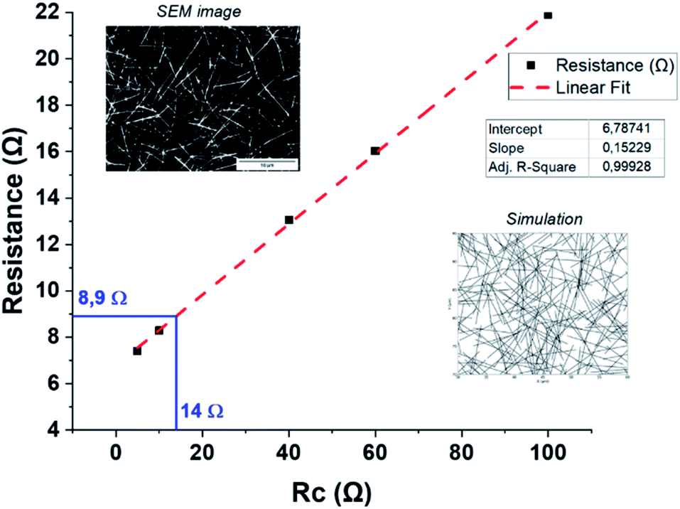 | ||
| Fig. 2 Determination of the average contact resistance between AgNWs: the simulated network sheet resistance is plotted versus the contact resistance (Rc) between two AgNWs. The computed Rs value is finally adjusted to the experimental one, leading to the correct estimated Rc value. SEM pictures of AgNW networks are used to extract the network density. For each arbitrary Rc value, 50 simulations were performed in order to average the randomness of the simulated networks. | ||
The deposited network was subjected to a continuous voltage ramp, with bias values large enough to degrade the network, as shown in Fig. 3a. As the voltage increases, so does the temperature, due to the Joule effect; the metallic nature of the conducting element leads to a slight increase of the resistance as temperature increases. The induced heating is confirmed by the temperature measured by using an IR camera; the maximum observed temperature, Tmax, is also reported in Fig. 3a. When the voltage bias reaches about 10 V, around 420 seconds after the beginning of the experiment, a significant and sharp increase in the resistance values is evidenced. Indeed, in less than 10 seconds, a sharp increase of five orders of magnitude is observed (from 10 Ω to MΩ). This is simultaneously accompanied by a sharp increase of Tmax, as shown in Fig. 3a. The series of IR images in Fig. 3b reveals that the location of the degradation also moved quickly throughout the entire sample. The green areas correspond to isothermal zones, i.e. where the temperature exceeds a specified threshold, here 195 °C. According to the series of images, the hotspots gradually shift from the centre of the specimen to the top and bottom edges. The resulting path follows a somewhat linear course parallel to the opposite electrodes. This extensive propagation is consistent with the electrical resistance increase, until the moment where the network is largely damaged and the electrical percolation is not spanning anymore from one electrode to the other. However, as previously described,14,17 one might observe that Rs returns to the 1 kΩ range after some time at rest. The critical current density jfailure was determined to be 1.63 × 10¹⁰ A m−2. The latter is in good agreement with the discussion reported in Lagrange et al.12 SEM images reveal a domain with degraded nanowires, where the network had been wiped out, as shown in Fig. 3c. These bands with a width of several μm, result from the local degradation of AgNWs and are at the origin of the sharp increase of the measured electrical resistance.
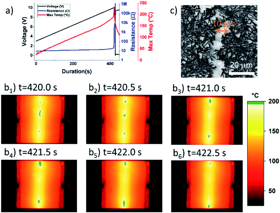 | ||
| Fig. 3 Experimental observation of the degradation of a spray deposited AgNW network. (a) Time evolution of resistance and maximum temperature on a AgNW network sample with an initial resistance of 8.9 Ω when applying a voltage ramp of 1 V min−1, starting from 3 V, until voltage breakdown was observed around 10 V. (b1–b6) Infrared images corresponding to the crack formation during the voltage ramp at different times between 420 and 422.5 s. Green areas represent the hottest regions, above 195 °C. A visible propagation of the hot-spot from the centre of the specimen to the edges, following a parallel line to the vertically aligned electrodes, is observed. (c) SEM image of the AgNW network degradation or “crack” visible due to the differences in the charging effect on the secondary electron detector. The width of the crack is about 10 μm. | ||
In order to establish a realistic simulation of this network evolution, a static 2D stick model was utilized to mimic the undamaged state. A 200 × 253 μm2 numerical sample was created for this purpose, with the same Lsx/Lsy ratio as the experimental substrate shown in Fig. 1a, and subjected to a 0.1 V voltage bias. The dynamic process described above was then applied to alter the simulated structure. The most stressed resistors were not scattered evenly across the sample. On the contrary, we observe a very strong geometric correlation within damaged resistors as the simulation progresses. In other words, the local breakdown of a resistor stresses the surrounding ones and makes them more likely to rupture during the following steps. This results in a well-defined and topologically controlled propagation process along a rather vertical crack (parallel to the electrodes), analogous to a mechanical crack. From the macroscopic standpoint, this induces the regular increase of the overall resistance of the system that was observed at each degradation step, as depicted in Fig. 4a. An example of the electrical current map is displayed in Fig. 4b after 75 steps corresponding to a macroscopic resistance of 16 Ω. The image shows a crack that appeared and further expanded to the middle of the specimen. The effect of the crack formation on the voltage map is represented with a series of images in Fig. 4c. The tip of the crack may actually be identified on the map (Fig. 4b) as the location where the current exhibits its highest value. The crack may be initiated anywhere within the sample. In the present case it was in the centre: this initial position is purely guided by the random generation of the network and should not be directly interpreted. In contrast, the crack propagation across the specimen occurs continuously. The strong dependence between the successive degraded links is the direct consequence of the positive feedback loop between the link degradation and the increase of current in the surrounding nanowires.
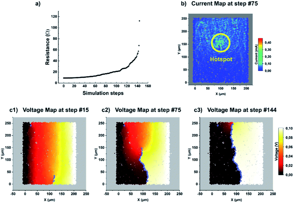 | ||
| Fig. 4 Degradation of the simulated AgNW network. (a) Evolution of resistance of the simulated planar network until loss of percolation. Each step corresponds to a gradual increase of the macroscopic resistance, by removing a selected resistor. (b) Electrical current map at step 75. The bright region shows the highest current values, i.e. a hotspot. (c) Voltage maps are shown at different steps (15, 75 and 144). Blue dots mark the position of the successive removed resistors, representing the formation of the crack, and the loss of the percolation paths. | ||
In order to better understand the phenomenon controlling the crack propagation, simulated networks were prepared with a well-defined notch. This flaw was first utilized to initiate the cracks on a known position, as shown in Fig. 5a. The notched specimens were modelled with the random stick simulation to determine the voltage and current maps, as described above. In addition, the surface current density and temperature of a homogeneous silver film with the same geometry were calculated using COMSOL Multiphysics software. In this simulation, the silver material was removed on a strip of 10 μm width. A 1 V voltage bias was then applied between the two opposite electrodes. As expected, the surface current density indicates a rather homogeneous distribution, except within the area that contains the notch, as clearly shown in Fig. 5b. In this case, the COMSOL simulation results in a 10 times increase of the current density at the tip of the defect, as compared to the homogeneous specimen case. A large tip-effect was already obtained, even for rather short notch of only 20 μm in length. This intense current density value results in a highly localized temperature increase, due to Joule heating. A steady-state temperature analysis is shown in Fig. 5c, with the sample still under a 1 V bias. This is the origin of the hotspot creation in an experimental AgNW network, as the temperature is higher in this region, causing a nanowire spheroidization and loss of electric contact.
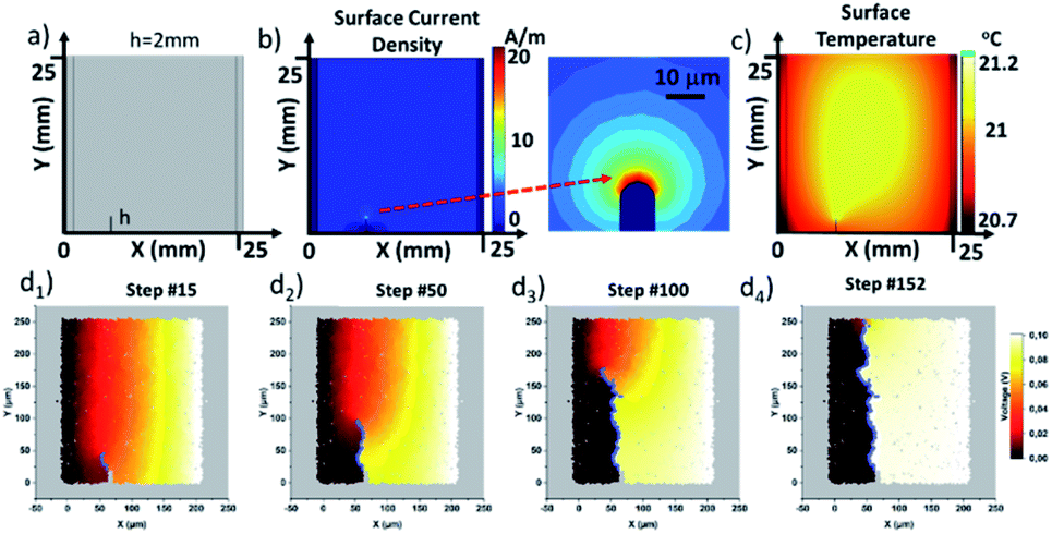 | ||
| Fig. 5 Modelling the degradation in a AgNW network with an initial notch. (a) Scheme of a silver film with a 2 mm vertical notch at the bottom left of a 25 × 25 mm sample. (b) COMSOL simulation of the surface current density under a 1 V bias applied between the vertical opposite electrodes. Entire sample, and zoom on the notch area. (c) COMSOL steady-state simulation of the surface temperature distribution under a 1 V bias. (d) Voltage maps at different steps (15, 50, 100 and 152) representing the formation of the crack in a network with a vertical notch on a 200 × 253 μm2 2D stick simulated network obtained with the model proposed in the present article. | ||
Therefore, considering the destruction of the network as a coupling electrical/thermal phenomenon, the simulation using the 2D network sticks reproduces this hypothesis. In the series of voltage maps shown in Fig. 5d, we observe the origin of the crack formation as the tip of the vertical defect. This origin point for the crack propagation is the region where the electrical power is the highest, associated with higher local temperature, and therefore causing a local degradation of the nanowires in this area. This dynamic model mimics the hotspot creation and the associated defect propagation to the nearby region, and the Joule heating induced region turns it to a hotspot, which degrades drastically the next nearby nanowires. This catastrophic phenomenon propagates as a domino effect.
Conclusions and prospects
In this study we present a dynamic model capable of simulating the onset of the degradation of a metallic nanowire network subjected to electrical stress. The main electrical and thermal features of the simulated networks are compared with those of equivalent AgNW networks experimentally deposited. We used dynamic simulations based on the 2D stick percolation theory. Our model was designed to allow the modification of the percolation cluster, and it shows good agreement with respect to macroscopic resistance, electrical potential distribution and generated heat. A thorough comparison enables the deduction of an average junction resistance value of 14 Ω. The network degradation mostly originated from randomly localized exacerbated Joule-heating, which consequently leads to the local degradation of the AgNWs in that particular region of the sample. This localized damage propagates as a domino effect finally leaving behind a very thin, vertical region where the percolative nature of the network is lost. Such a region, following a strong analogy with a mechanical crack, destroys the electrical conduction paths. Our model also shows that regions with small defects can be the source of such hotspots, therefore inducing the electrical degradation of the whole specimen. The existence of a microscopic defect induces a large instability on the current density values along some tens of microns distance. Consequently, these simulations show also that the Joule heating in the edge of defects is much more significant than for the rest of the specimen, and thus it represents a plausible origin of a hotspot, as those experimentally observed. As a result, the present model provides deeper explanations related to the degradation mechanisms of metallic nanowire networks that have been experimentally observed, and thus paves the way for a better understanding of network failure. This is a necessary step to overcome instability issues in metallic nanowire based transparent electrodes in order to successfully integrate them into industrial devices.Conflicts of interest
There are no conflicts to declare.Acknowledgements
This work was performed within the framework of the Centre of Excellence of Multifunctional Architectured Materials (CEMAM) no. ANR-10-LABX-44-01. Agence Nationale de la Recherche (ANR) is acknowledged for financial support under contracts ANR-18-CE09-0040 (MEANING) and ANR-18-CE09-0036 (PANASSE). NC thanks Csaba Forró and Olivier Caudrelier for fruitful discussions.References
- D. S. Hecht, L. Hu and G. Irvin, Adv. Mater., 2011, 23, 1482–1513 CrossRef CAS.
- K. McLellan, Y. Yoon, S. N. Leung and S. H. Ko, Adv. Mater. Technol., 2020, 5, 1900939 CrossRef CAS.
- K. Ellmer, Nat. Photonics, 2012, 6, 809–817 CrossRef CAS.
- D. Bellet, M. Lagrange, T. Sannicolo, S. Aghazadehchors, V. Nguyen, D. Langley, D. Muñoz-Rojas, C. Jiménez, Y. Bréchet and N. Nguyen, Materials, 2017, 10, 570 CrossRef.
- T. Sannicolo, M. Lagrange, A. Cabos, C. Celle, J.-P. Simonato and D. Bellet, Small, 2016, 12, 6052–6075 CrossRef CAS.
- Y. Sun, M. Chang, L. Meng, X. Wan, H. Gao, Y. Zhang, K. Zhao, Z. Sun, C. Li, S. Liu, H. Wang, J. Liang and Y. Chen, Nat. Electron., 2019, 2, 513–520 CrossRef CAS.
- A. G. Ricciardulli, S. Yang, G.-J. A. H. Wetzelaer, X. Feng and P. W. M. Blom, Adv. Funct. Mater., 2018, 28, 1706010 CrossRef.
- J. Wang, J. Jiu, T. Araki, M. Nogi, T. Sugahara, S. Nagao, H. Koga, P. He and K. Suganuma, Nano-Micro Lett., 2014, 7, 51–58 CrossRef.
- D. T. Papanastasiou, A. Schultheiss, D. Muñoz-Rojas, C. Celle, A. Carella, J.-P. Simonato and D. Bellet, Adv. Funct. Mater., 2020, 1910225 CrossRef CAS.
- H. H. Khaligh and I. A. Goldthorpe, Nanoscale Res. Lett., 2013, 8, 235 CrossRef.
- D. Chen, F. Zhao, K. Tong, G. Saldanha, C. Liu and Q. Pei, Adv. Electron. Mater., 2016, 2, 1600167 CrossRef.
- M. Lagrange, T. Sannicolo, D. Muñoz-Rojas, B. G. Lohan, A. Khan, M. Anikin, C. Jiménez, F. Bruckert, Y. Bréchet and D. Bellet, Nanotechnology, 2016, 28, 055709 CrossRef.
- D. P. Langley, M. Lagrange, G. Giusti, C. Jiménez, Y. Bréchet, N. D. Nguyen and D. Bellet, Nanoscale, 2014, 6, 13535–13543 RSC.
- T. Sannicolo, N. Charvin, L. Flandin, S. Kraus, D. T. Papanastasiou, C. Celle, J.-P. Simonato, D. Muñoz-Rojas, C. Jiménez and D. Bellet, ACS Nano, 2018, 12, 4648–4659 CrossRef CAS.
- J. Lienig and M. Thiele, Fundamentals of Electromigration-Aware Integrated Circuit Design, Springer Publishing Company, Incorporated, 1st edn, 2018 Search PubMed.
- T.-B. Song, Y. Chen, C.-H. Chung, Y. M. Yang, B. Bob, H.-S. Duan, G. Li, K.-N. Tu, Y. Huang and Y. Yang, ACS Nano, 2014, 8, 2804–2811 CrossRef CAS.
- F. N. Kholid, H. Huang, Y. Zhang and H. J. Fan, Nanotechnology, 2015, 27, 025703 CrossRef.
- R. Benda, B. Lebental and E. Cancès, J. Appl. Phys., 2019, 126, 044306 CrossRef.
- D. Langley, G. Giusti, M. Lagrange, R. Collins, C. Jiménez, Y. Bréchet and D. Bellet, Sol. Energy Mater. Sol. Cells, 2014, 125, 318–324 CrossRef CAS.
- D. P. Langley, M. Lagrange, N. D. Nguyen and D. Bellet, Nanoscale Horiz., 2018, 3, 545–550 RSC.
- R. M. Mutiso and K. I. Winey, Phys. Rev. E, 2013, 88, 032134 CrossRef.
- S. De, T. M. Higgins, P. E. Lyons, E. M. Doherty, P. N. Nirmalraj, W. J. Blau, J. J. Boland and J. N. Coleman, ACS Nano, 2009, 3, 1767–1774 CrossRef CAS.
- C. Forró, L. Demkó, S. Weydert, J. Vörös and K. Tybrandt, ACS Nano, 2018, 12, 11080–11087 CrossRef.
- R. M. Mutiso, M. C. Sherrott, A. R. Rathmell, B. J. Wiley and K. I. Winey, ACS Nano, 2013, 7, 7654–7663 CrossRef CAS.
- C. Mayousse, C. Celle, E. Moreau, J.-F. Mainguet, A. Carella and J.-P. Simonato, Nanotechnology, 2013, 24, 215501 CrossRef.
- C. G. da Rocha, H. G. Manning, C. O'Callaghan, C. Ritter, A. T. Bellew, J. J. Boland and M. S. Ferreira, Nanoscale, 2015, 7, 13011–13016 RSC.
- A. A. Hagberg, D. A. Schult and P. J. Swart, Proceedings of the 7th Python in Science Conference, Pasadena, CA USA, 2008, pp. 11–15 Search PubMed.
- A. Bid, A. Bora and A. K. Raychaudhuri, Phys. Rev. B: Condens. Matter Mater. Phys., 2006, 74, 035426 CrossRef.
- J.-Y. Lee, S. T. Connor, Y. Cui and P. Peumans, Nano Lett., 2008, 8, 689–692 CrossRef CAS.
- F. Selzer, C. Floresca, D. Kneppe, L. Bormann, C. Sachse, N. Weiß, A. Eychmüller, A. Amassian, L. Müller-Meskamp and K. Leo, Appl. Phys. Lett., 2016, 108, 163302 CrossRef.
- A. T. Bellew, H. G. Manning, C. G. da Rocha, M. S. Ferreira and J. J. Boland, ACS Nano, 2015, 9, 11422–11429 CrossRef CAS.
- F. Völklein, H. Reith, T. W. Cornelius, M. Rauber and R. Neumann, Nanotechnology, 2009, 20, 325706 CrossRef.
| This journal is © The Royal Society of Chemistry 2021 |