
 Open Access Article
 This Open Access Article is licensed under a Creative Commons Attribution-Non Commercial 3.0 Unported Licence
Composition and properties of RF-sputter deposited titanium dioxide thin films†
Jesse
Daughtry
 ab,
Abdulrahman S.
Alotabi
ab,
Liam
Howard-Fabretto
ab and
Gunther G.
Andersson
*ab
ab,
Abdulrahman S.
Alotabi
ab,
Liam
Howard-Fabretto
ab and
Gunther G.
Andersson
*ab
aFlinders Institute for NanoScale Science and Technology, Flinders University, Adelaide, SA 5001, Australia. E-mail: gunther.andersson@flinders.edu.au
bFlinders Microscopy and Microanalysis, College of Science and Engineering, Flinders University, Adelaide, SA 5042, Australia
First published on 8th December 2020
Abstract
The photocatalytic properties of titania (TiO2) have prompted research utilising its useful ability to convert solar energy into electron–hole pairs to drive novel chemistry. The aim of the present work is to examine the properties required for a synthetic method capable of producing thin TiO2 films, with well defined, easily modifiable characteristics. Presented here is a method of synthesis of TiO2 nanoparticulate thin films generated using RF plasma capable of homogenous depositions with known elemental composition and modifiable properties at a far lower cost than single-crystal TiO2. Multiple depositions regimes were examined for their effect on overall chemical composition and to minimise the unwanted contaminant, carbon, from the final film. The resulting TiO2 films can be easily modified through heating to further induce defects and change the electronic structure, crystallinity, surface morphology and roughness of the deposited thin film.
Introduction
Titania (TiO2) has been a major area of research since the discovery of its photocatalytic properties in 1972.1 Since then, TiO2 has been one of the most widely studied semiconductors, driven largely due to its non-toxic nature, low cost, stability, and varied methods of synthesis and property control.2–4 The broad range of possible applications stems from its versatile photocatalytic properties. The activity of this material under UV light has led to its inclusion in many sun protection applications,5 sensors,2 integrated optical devices,6 photo-oxidation of pollutants and dangerous chemicals,7 and photocatalytic processes for energy storage.8 All of these applications utilise TiO2 in the form of nanoparticulate coatings,9 making scalable, affordable synthesis of such coatings valuable, especially if they can be modified for specific properties.The synthesis of TiO2 amorphous films, thin layers of nanoparticle sized TiO2 has been achieved through a variety of techniques such as chemical vapour deposition (CVD),10 sol–gel processing11,12 atomic layer deposition13 and direct current (DC) and radio frequency (RF) magnetron sputtering processes.14,15 These final two sputtering methods have been widely explored due to their stability, reproducibility, ease of use and deposition control over a variety of substrates. The films deposited through this method are commonly dense, closed layers of nanoparticulate TiO2. Nanoparticle Titania has shown particular promise across the range of possible applications and also offers a level of control over characteristics such as particle size,16 phase-type17,18 and stoichiometry.17
The use of well-understood TiO2 nanoparticle thin films is especially useful for surface science studies utilising photoelectron spectroscopy. Several valuable techniques for probing electronic structure such as X-ray photoelectron spectroscopy (XPS) and ultraviolet photoelectron spectroscopy (UPS) require precision knowledge of a sample's elemental composition and electronic structure to yield meaningful results.19,20 Many photocatalytic systems require a robust substrate–catalyst electronic interaction to prevent changes in the performance of the catalyst due to agglomeration; one method proposed to achieve this is defect rich surfaces.21,22 Ti3+ defects have been explored as promising binding sites for heterogeneous catalysts that offer strong electronic interaction to prevent agglomeration.23,24
The topography, crystallinity and particulate characteristics have been well established in sputtered thin films using atomic force microscopy (AFM),6,25 scanning electron microscopy (SEM)18,26 and X-ray diffraction (XRD).6,16,18 However, the elemental composition of the final coating is relatively unexplored for RF sputtered TiO2. Carbon-containing substances like hydrocarbons are considered as a contaminant for many methods of electron spectroscopy and is present in considerable quantities for many commonly used methods of TiO2 synthesis. Hence, an RF sputtered deposition procedure resulting in low carbon percentage is desirable. Single crystal TiO2 is also capable of addressing the issue of contamination but is prohibitively expensive for applications on a larger scale.
TiO2 can be either amorphous or has one of three crystalline forms: anatase, brookite or rutile. Layers or films of titania can be either pure or mixtures of these forms with synthetic methods often influencing the structure of the coating through control of factors such as deposition temperature,26 or by post-deposition treatments.6,27 The surface morphology and crystal phase composition of TiO2 films are also modifiable through post-deposition calcination and have been shown to influence and improve the photocatalytic properties of deposited films.28
The present study demonstrates a method of depositing RF sputtered TiO2 thin films onto Si(110) substrates, with a range of target pre-treatments, deposition lengths and annealing as post-treatment. Systematic studies into elemental composition, morphology, crystallinity and chemical state of the nanoparticulate TiO2 were conducted to determine their composition, contaminants and ease of surface modification with Ti3+ defects. The results indicate that one method, in particular, produced a TiO2 nanoparticulate film capable of low-cost scalability, minimal carbon contamination in the final film and simple modification of surface defects, crystallinity and surface morphology.
Experimental details
Preparation of TiO2 thin films
TiO2 thin films used in this work were prepared at room temperature using an RF magnetron sputtering system. High purity 2-inch (99.9%) TiO2 targets were used to deposit TiO2 nanoparticles onto 4-inch diameter Si(110) substrates. 2 TiO2 targets were used, one having been used for several months, the other being brand new, to determine how target ageing affects the resultant deposition quality. The substrates were cleaned with ethanol and acetone for 15 min in an ultrasonic bath. The substrates were then dried under nitrogen. The deposition was done three times, with differing chamber/target conditions. Firstly after 1.5 hours of pre-sputtering to clean the target and chamber (designated 90m-RF), secondly after 30 min of pre-sputtering for cleaning (designated 30m-RF) and finally with an unused TiO2 target after 30 min pre-sputtering (designated FT-RF). The sputter deposition was performed in all cases with a chamber pressure of at least 2 × 10⁻⁵ mbar, with 5 ccm pure argon flowing, 500 W magnetron power and a working distance of 14 cm. These conditions provided a deposition rate of approximately 180 nm h−1. The deposition took place at room temperature with no substrate heating.All samples were cut into 1 × 1 cm squares using a diamond-tipped silicon cutter to minimise surface contact and contamination. Particulate dust from cutting was removed with pressurised dry nitrogen. Samples were then mounted to molybdenum sample holders and inserted into the ultra-high vacuum chamber (9.2–6 × 10⁻¹⁰ mbar). The samples were characterised in this unaltered condition (designated by the As-made tag next to sample name) before the samples were heated through filament emission heating to 500 °C and held there for 10 minutes in an attempt to reduce film contaminants. XPS scans marked “heated” were taken almost immediately after heating.
Samples from all deposition methods were measured in As-made condition as well as after heating to 500 °C in UHV. Further, post-deposition heating was performed on a single sample prepared from the FT-RF method in vacuum at 300 °C, 500 °C and 700 °C (see Table 1) in succession with photoelectron measurements taken after 30 minutes of heating at a given temperature before increasing the temperature. The sample designated “300 °C and Ar sputtered” was heated to 300° as described previously and then immediately exposed to an argon ion sputter beam, exposing the sample surface with a dose of 6 × 10¹⁴ ions, controlled through exposure time dependant on ion current (see ESI S1†). FT-RF samples were also heated up to 1100 °C in atmospheric conditions for crystal phase structure investigations.
| Deposition methods | FT-RF TiO2 – vacuum heated series, treatment |
|---|---|
| FT-RF | 300 °C |
| 30m-RF | 500 °C |
| 90m-RF | 700 °C |
Additionally, electron spectroscopy measurements were taken from rutile (110) single crystal (SC). The SC TiO2 was pre-treated at 877 °C (1150 K) ex situ to induce bulk defects, making the sample conductive and useful for electron spectroscopy. The SC TiO2 again was heated to 625 °C in situ immediately before photoelectron measurements to produce surface defects, the XPS relative elemental composition of SC TiO2 can be seen in Table S3.†
Spectroscopy
Microscopy
Once the levels of unwanted contaminants were determined, and the best candidate surface (FT-RF) was selected, further analysis of the morphological characteristics of the film was performed using AFM and SEM techniques. Samples were prepared by identical cutting and cleaning procedures, with selected samples being heated in an air-atmosphere furnace at the required temperature before mounting onto flat or vertical SEM stubs as necessary. All SEM measurements were performed on the samples as they are.Results and discussion
Chemical composition
XP spectra were taken at the C 1s, O 2s, Ti 2p, Si 2p, F 1s and Na 1s regions for all samples. The breakdown of peak positions found in each region is presented in detail in the ESI (S2†) and the relative intensities in Table 2. The carbon in the sample is mostly attributed to adventitious hydrocarbons, and the C 1s peak is assigned to 285 eV. This peak is very consistent in its energy position and therefore, suitable for use in calibration.33 The oxygen signal is attributed mostly to titanium dioxide (530.3 ± 01 eV) with some minimal contribution from silicon dioxide (532.3 ± 0.1 eV), the high relative percentage of oxygen is discussed later in this text when describing the results shown in Fig. 1. The titanium signal is exclusively due to the nanoparticle thin film, and the dominant species (Ti4+) is assigned to 459.3 ± 0.1 eV with titanium defects induced through sample treatments (Ti3+) assigned to 457.6 ± 0.1 eV. The silicon signal is due to SiO2 from the silicon wafer used as a substrate and is found at 102.4 ± 0.1 eV. Both sodium (1071.2 ± 0.1 eV) and fluorine (685.4 ± 0.1 eV) were contaminants of unknown origin with fluorine only found in one sample, while Sodium appeared in varying concentrations in all but FT-RF-As-made and is likely due to sample handling prior to the XPS measurements.| XPS relative elemental composition (%) | ||||||
|---|---|---|---|---|---|---|
| Carbon | Oxygen | Titanium | Silicon | Fluorine | Sodium | |
| FT-RF-As-made | 20.2 ± 0.1 | 60.4 ± 0.1 | 18.2 ± 0.1 | 0.2 ± 0.1 | 0.9 ± 0.1 | 0.00 |
| 30m-RF-As-made | 14.6 ± 0.1 | 61.3 ± 0.1 | 18.5 ± 0.1 | 0.1 ± 0.1 | 0.00 | 5.5 ± 0.1 |
| 90m-RF-As-made | 26.8 ± 0.1 | 54.8 ± 0.1 | 16.7 ± 0.1 | 1.1 ± 0.1 | 0.00 | 1.7 ± 0.1 |
| FT-RF – heated | 5.9 ± 0.1 | 72.1 ± 0.1 | 20.1 ± 0.1 | 0.5 ± 0.1 | 0.00 | 1.5 ± 0.1 |
| 30m-RF – heated | 8.7 ± 0.1 | 57.1 ± 0.1 | 20.8 ± 0.1 | 5.0 ± 0.1 | 0.00 | 9.2 ± 0.1 |
| 90m-RF – heated | 20.5 ± 0.1 | 57.4 ± 0.1 | 19.1 ± 0.1 | 0.6 ± 0.1 | 0.00 | 2.3 ± 0.1 |
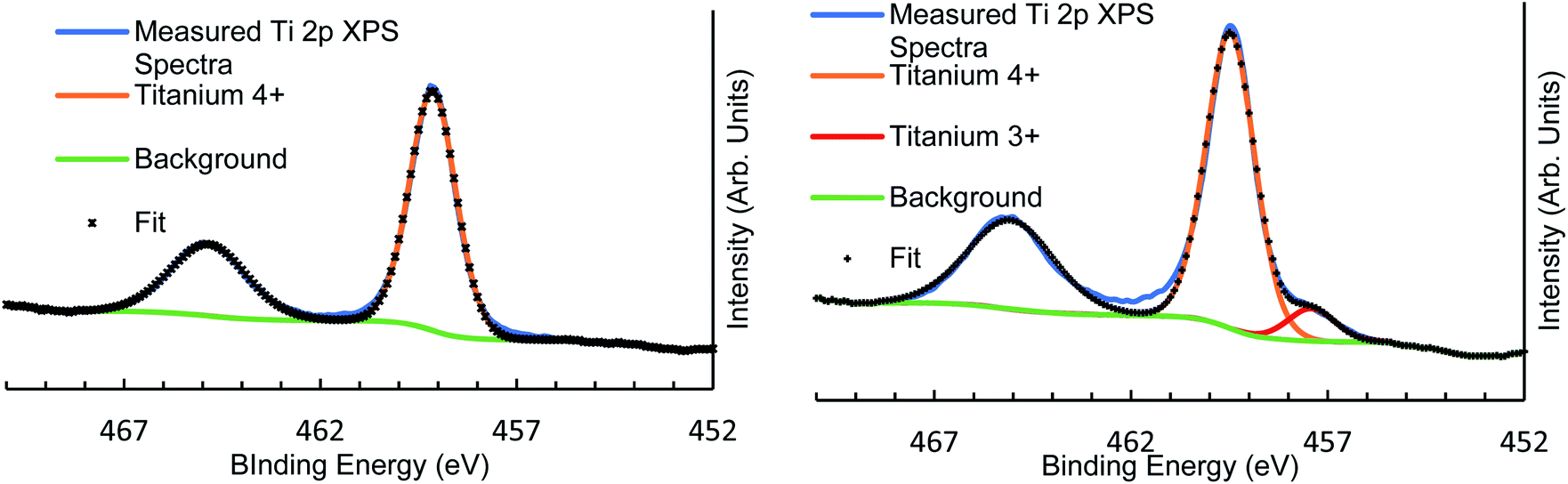 | ||
| Fig. 1 XPS high-resolution scan fitting for vacuum heated Ti 2p region showing As-made (left) and 500 °C heated (right) with Ti3+ defect showing in the heated sample at around 457 eV binding energy. | ||
The XPS scans of these samples (Fig. 1, fits can be found in Table S2†) revealed several trends and characteristics. Across all samples, the ratio of Ti 2p orbital signature to O 1s is around 3.1![[thin space (1/6-em)]](https://www.rsc.org/images/entities/char_2009.gif) :1 (O:Ti) with O accounting for an average of 60% of the measured signal while Ti accounts for approximately 20%. These values, while not stoichiometrically expected, are both consistent between the three prepared surfaces as well as comparisons to previously measured P-25 and atomic layer deposited TiO2 surfaces measured using the same experimental equipment34 and as such are seen as representative of TiO2. One possible reason for non-stoichiometric O concentration is adsorbed O species such as OH and H2O. Another possible reason is an inaccuracy in the sensitivity factor applied for the O 1s XPS intensity.
:1 (O:Ti) with O accounting for an average of 60% of the measured signal while Ti accounts for approximately 20%. These values, while not stoichiometrically expected, are both consistent between the three prepared surfaces as well as comparisons to previously measured P-25 and atomic layer deposited TiO2 surfaces measured using the same experimental equipment34 and as such are seen as representative of TiO2. One possible reason for non-stoichiometric O concentration is adsorbed O species such as OH and H2O. Another possible reason is an inaccuracy in the sensitivity factor applied for the O 1s XPS intensity.
Surface contaminants, a particular concern when using synthesised thin films for surface-sensitive measurements, were also determined through their characteristic XPS orbital signatures (Table 3). Carbon (1s) was the most apparent contaminant with every sample showing some noticeable percentage of carbon (between 6–26%) mainly due to adventitious carbon.35 The highest levels of C 1s signal were found in as-made samples which had been exposed to the atmosphere after deposition and before undergoing heating, as would be expected. The 90m-RF sample was particularly carbonaceous in both as-made and post-heated form, indicating that a longer pre-cleaning time increases the carbon content within the final film, counter to the processes intent. The surface prepared through the fresh TiO2 target (FT-RF) was the least carbonaceous of the three methods.
| FT-RF:vacuum heated series | Carbon | Oxygen | Titanium | Ti3+ defect | Silicon | Fluorine |
|---|---|---|---|---|---|---|
| As-made | 26.0 ± 0.1 | 54.7 ± 0.1 | 18.1 ± 0.1 | 0.00 | 0.5 ± 0.1 | 0.7 ± 0.1 |
| 300 °C | 5.1 ± 0.1 | 72.1 ± 0.1 | 21.4 ± 0.1 | 1.2 ± 0.1 | 0.6 ± 0.1 | 0.7 ± 0.1 |
| 500 °C | 4.8 ± 0.1 | 71.6 ± 0.1 | 22.8 ± 0.1 | 1.7 ± 0.1 | 0.8 ± 0.1 | 0.00 |
| 700 °C | 5.6 ± 0.1 | 70.3 ± 0.1 | 22.5 ± 0.1 | 1.6 ± 0.1 | 1.6 ± 0.1 | 0.00 |
| 300 °C + Ar sputtered | 4.4 ± 0.1 | 68.8 ± 0.1 | 26.1 ± 0.1 | 4.5 ± 0.1 | 0.8 ± 0.1 | 0.00 |
Silicon signal was below 1.1% for all samples; this elemental presence may be at least partly attributable to an intermixing of Ti and Si during the RF deposition. The only exception was for the 30m-RF-As-made, which showed approx. 5% Si after heating, probably due to film spallation36 revealing some bare Si. This, coupled with the observation that while in previous studies on TiO2 film depositions Si 2p were detected at a binding energy of 99.8 ± 0.3 eV,34 all Si signal from these samples is observed at 102.3 ± 0.3 eV. This binding energy points towards the presence of organic silicon compounds. The RF-sputter deposition process likely results in the formation of small amounts of silicate species37 or a Si–O–Ti compound formed during deposition.
Previous spectroscopic studies on systems utilising TiO2 have had issues with Si and C signal interfering with sensitive data collection and analysis.34 These contaminant species are found to be present in all samples prepared through RF sputter deposition. However, the sample prepared from the fresh target of TiO2 showed negligible Si 2p signal and a very low concentration of C 1s, further lessened through heating in vacuum, making it the best candidate for sensitive surface spectroscopic studies.
Other contaminants were minimal. Fluorine (1s) was observed in the fresh target sample before heating at 1% of the surface signal. However, heating removed this signal to below detectable amounts. Sodium (1s) was also detected although the variability of Na in samples from the same deposition proves suggests this contamination is due to sample processing. However, after heating, all sodium-containing samples had their sodium content increase, raising the possibility that some sub-surface Na may be drawn to the surface through heating processes. This interpretation would be consistent with the observed low surface energy of Na, causing it to migrate towards the surface of metal oxides during heating processes and electron beam exposure.38,39 Samples from the FT-RF:vacuum heated series were heated under UHV conditions to analyse any compositional/electronic changes that might be induced. Calcination of FT-RF samples was performed over a range of temperatures under UHV conditions (Table 3). It can be seen that calcination as low as 300 °C was able to produce a significant reduction in C XPS signal, with a further slight C reduction at 500 °C before an increase in C contribution was observed for heating at 700 °C. The increase in C at 700 °C was accompanied by an increased Si contribution, pointing toward the onset of film spallation at this temperature, consistent with previous reports on TiO2 thin films.36 This process exposes small regions of the Si substrate through cracks in the film, simultaneously exposing C impregnated in the bulk of the TiO2 film. To further explore this, an FT-RF sample was heated to 300 °C before being exposed to a dose of sputtering Ar ions. Sputter treatment should preferentially remove any C present at the surface of the film, while bulk C signal is unaffected. The 300 °C + Ar sputter treatment as can be seen (Table 3) to result in the lowest C contribution compared to a purely heated sample at 4.4 ± 0.1% of XPS relative composition. The C signal in the 300 °C + Ar sputter treatment is therefore assumed to be a baseline C contribution through RF sputtered deposition, as it would not be removable without compromising the integrity and coverage of the TiO2 layer.
The XPS elemental relative concentrations seen in Table 3 show that heating under vacuum to higher temperatures induced Ti3+ defects at around 457.3 ± 0.1 eV binding energy (Fig. 1). These defects increase as a relative proportion of total Ti 2p signal with heating, as seen in Table 4. The highest proportion of Ti3+ defects are seen in the 300 °C and Ar sputtered sample, which registered 17.1% of all Ti XPS signal as Ti3+ defect. The sputter treatment also decreased the overall O XPS signal in the sample, indicating that these defects were the result of oxygen vacancies induced through the sputter dose. Exposure to atmosphere quenched all previously measured Ti3+ signal. The relative ease with which such defects can be induced is a useful surface modification for use in studies of heterogeneous photocatalytic systems.
| Vacuum heated FT-RF | |
|---|---|
| 300 °C | 5.4% |
| 500 °C | 7.5% |
| 700 °C | 6.9% |
| 300 °C + Ar sputtered | 17.1% |
The UPS scans of the heated range reveal the changing electronic structure of the TiO2 nanoparticles as they are heated, energies above 10 eV are affected by secondary electrons and as such are not considered here. The electronic features seen in heated RF-TiO2 in the region from 3–9 eV are consistent with several previously reported studies examining the features found in DOS of modified TiO2 and are reported to be from O(2p) species.40,41
Krischok et al. identify the peak around 4.5 eV as being associated with the ionisation of oxygen states in the upper valence band, mainly from bridging oxygen in the TiO2, it can be seen that all four spectra in Fig. 2 share this peak's energy position. The visible decrease in the 4.5 eV peak over the heated range of samples corresponds with a loss of the bridging oxygen, giving rise to the observed increase in Ti3+ defects in Table 4.
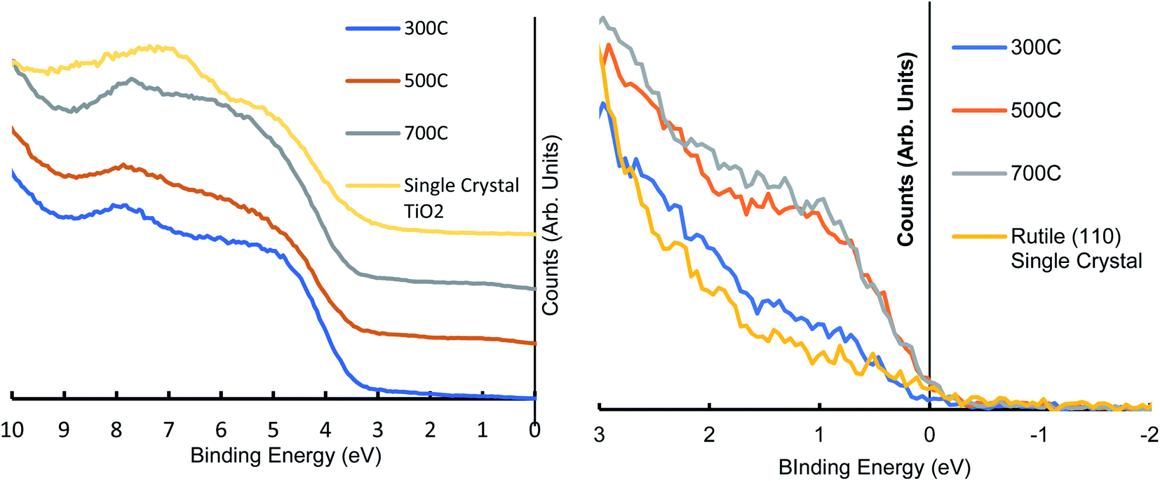 | ||
| Fig. 2 UPS scans from a range of heated FT-RF samples and rutile (110) single crystal TiO2 showing broad range electronic structure on the left (series are offset in the y-axis) and the near-Fermi valence band on the right. | ||
The 8 eV peak originates from oxygen species in the oxygen plane of the TiO2 surface.42,43 While the single-crystal TiO2 shares the 4.5 eV peak with RF-TiO2 samples, the single crystal displays a shifted oxygen plane energy peak at around 7 eV compared to the RF-TiO2 which appears at around 8 eV. This kind of variance in TiO2 UPS spectra is not unexpected, as similar differences have previously been observed.44,45 One possible reason for such a shift could be attributed to the lower work function of the single crystal TiO2.42
The near-Fermi region shows a clear peak centred at 1 eV is attributed to the Ti3+ defect and shows an apparent increase at higher temperatures for the RF-sputtered films, in agreement with XPS observations. The UPS spectra of the RF sputtered TiO2 shows higher signal around 1 eV, attributed to Ti3+ defects, when compared to single-crystal TiO2 showing its suitability for surface modification, even at lower calcination temperatures.
Morphological characterisations
Fig. 3 shows the uniformly distributed nature of the nanoparticulate film deposited through RF-TiO2 deposition. SEM on a vertically mounted sample (Fig. S2†) showed the deposited TiO2 film having a thickness of 150 ± 5 nm across the film's cross-section. | ||
| Fig. 3 AFM scans on (A) As-made, 1 × 1 μm (B) 500 °C vacuum heated, 1 × 1 μm (C) As-made, 3 × 3 μm (D) 500 °C vacuum heated, 3 × 3 μm. | ||
Comparison between Fig. 3A–D shows differences between the as-made and vacuum heated samples. The relatively smooth, close-packed nature of the film was observed across the sample surface, and in as-made condition consists of roughly spherical particles approximately 25–45 nm in diameter (Fig. 3A). While the sample heated to 500 °C appears to show a lack of spherical particles and the appearance of larger particles of arbitrary shape, possibly through the ripening of the TiO2 under vacuum heating conditions. The 3 μm scans (Fig. 3C and D) show more significant regions separated by boundaries on the surface of increased height in both the as-made and vacuum heated samples. Again the vacuum heated sample displays less defined particles and a noticeable flattening of the film surface when compared to the as-made sample viewed at the same magnification.
The roughness parameters (Rq root-mean-squared average roughness, Ra mean surface roughness) values for the heated samples have also decreased from the as-made samples to the heated samples (see Table 5). This change confirms that the RF-TiO2 deposited film has undergone some level of rearrangement from the as-made, nanoparticulate form into a flatter, more aligned surface. High-resolution images in the ESI (Fig. S3†) show that these spherical particles grow to larger sizes after heating to higher temperatures. Previous work has attributed these changes to an increase in crystallinity of TiO2 and smaller particles' ripening into larger ones.6,16,46
| Roughness parameters | 500 °C vacuum heated (nm) | As-made (nm) |
|---|---|---|
| R q | 0.76 ± 0.01 | 1.06 ± 0.12 |
| R a | 0.60 ± 0.03 | 0.84 ± 0.08 |
The large agglomerations of particles seen in Fig. 3C seem to have transitioned into the raised lines visible in Fig. 3D that divide the film into rough regions. These same phenomena can be observed in Fig. 4; once calcination temperatures reached >900 °C the resultant condition of the coating was that of well-defined grain boundaries containing regions of varying size. At 1100 °C, some of these regions showed a visibly distinct texture with increased roughness, potentially related to a crystal phase transition observed in samples heated to this temperature.
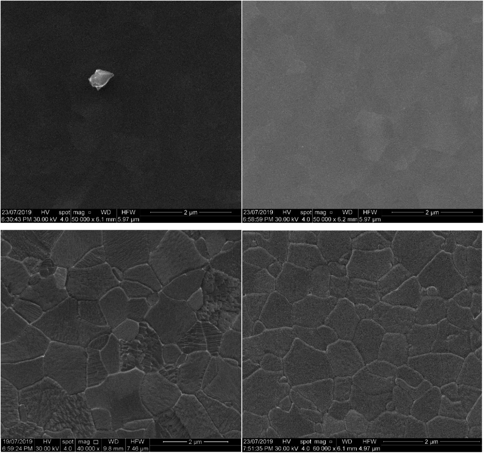 | ||
| Fig. 4 SEM scans showing the morphological changes to FT-RF sputtered TiO2 films as they are heated, clockwise from top left, 500 °C 1 h, 600 °C 1 h, 900 °C 1 h, 1100 °C 24 h. The particle shown in the 500 °C image was included to aid focussing of the measurement. | ||
Crystal structure
Samples measured with XRD are shown with offset intensities in Fig. 5 and spanned a range from (i) Si, (ii) as-made RF-TiO2, (iii) as-made atomic layer deposition TiO2, (iv) 500 °C atmosphere heated RF-TiO2 (1 h), (v) 600 °C atmosphere heated RF-TiO2 (1 h), (vi) 900 °C atmosphere heated RF-TiO2 (3 h) and (vii) 1100 °C atmosphere heated RF-TiO2 (24 h) and (viii) 1100 °C atmosphere heated RF-TiO2 (24 h). The reference spectra for anatase and rutile TiO2 calculated using the materials project are displayed in Fig. 5, showing the reference peaks for the respective TiO2 phases. | ||
| Fig. 5 Offset XRD scans on as-made and heated samples showing the transition from amorphous TiO2 towards anatase phase. Rutile phase formation was detected only within the 1100 °C heated sample. Anatase and rutile main XRD peaks shown on the x-axis, in blue and orange respectively. XRD spectra shown are XRD spectra shown are (i) Si, (ii) as-made RF-TiO2, (iii) as-made atomic layer deposition TiO2, (iv) 500 °C atmosphere heated RF-TiO2 (1 h), (v) 600 °C atmosphere heated RF-TiO2 (1 h), (vi) 900 °C atmosphere heated RF-TiO2 (3 h) and (vii) 1100 °C atmosphere heated RF-TiO2 (24 h). | ||
The change in crystallinity in systems such as reactively sputtered TiO2 films and sol–gel crystallised TiO2 have previously found the phase transition to rutile phase to occur at around 600 °C with film thickness and temperature being critical factors in the phase transition.17,37 The system studied here shows markedly different crystallisation behaviour. We see in Fig. 5 that the onset of anatase phase TiO2 appears from 500 °C heated samples, up to 900 °C with no corresponding rutile phase emerging. The emergence of Rutile crystal peaks in the XRD is seen only in 1100 °C samples heated for > 18 hours. This high temperature required produced samples with distinct, peaks for anatase and rutile phases, with an approximate 1:1 ratio in the peak areas.
The time-dependence and the elevated temperature necessary to attain rutile TiO2 are distinct from critical factors reported in phase transitions for other TiO2 synthetic methods. The significant differences in crystallisation temperatures for anatase and rutile phases offer the potential of controlling substrates for required phases type and ratio with post-deposition treatments.
Conclusions
This paper details the successful deposition of RF-sputtered TiO2 films onto Si (110) substrates from TiO2 targets with a range of deposition processes. The chemical composition, particularly with regards to the presence of contaminant species undesirable in surface-sensitive photoelectron studies was determined for a range of different deposition conditions. The results of these studies indicated that for minimal contaminant surface species the use of 30 minutes of pre-cleaning of the sputter target and the use of a new, ‘fresh’ TiO2 target produced the surface with lowest concentrations of Si (<1%) and C (6%) achieved through heating to 500 °C under vacuum. These films are capable of modification through heating to induce Ti3+ defect sites. Morphological studies revealed that these films consisted of close-packed, films of circular nanoparticles 20–30 nm in size. Heating of the films increased the surface roughness and particle size of the TiO2. The crystallinity of the substrate is capable of being tuned for anatase or an anatase/rutile mixture with heating between 500–1100 °C for extended periods (18–24 h).Conflicts of interest
There are no conflicts to declare.Acknowledgements
Part of this research was undertaken on the soft X-ray spectroscopy beamline at the Australian Synchrotron, Victoria, Australia (AS1/SXR/15819). The work is supported by the US army project FA5209-16-R-0017. The authors acknowledge the facilities, and the scientific and technical assistance, of Microscopy Australia (formerly known as AMMRF) and the Australian National Fabrication Facility (ANFF) at Flinders University. The authors acknowledge Flinders Microscopy and Microanalysis and their expertise. The authors acknowledge Dr Cameron Shearer from the University of Adelaide for his support in running the XRD measurements.References
- A. Fujishima and K. Honda, Electrochemical Photolysis of Water at a Semiconductor Electrode, Nature, 1972, 238, 37–38 CrossRef CAS.
- A. N. Shipway, E. Katz and I. Willner, Nanoparticle arrays on surfaces for electronic, optical, and sensor applications, ChemPhysChem, 2000, 1, 18–52 CrossRef CAS.
- M. Pelaez, N. T. Nolan, S. C. Pillai, M. K. Seery, P. Falaras, A. G. Kontos, P. S. Dunlop, J. W. Hamilton, J. A. Byrne and K. O'shea, A review on the visible light active titanium dioxide photocatalysts for environmental applications, Appl. Catal., B, 2012, 125, 331–349 CrossRef CAS.
- M. Cargnello, T. R. Gordon and C. B. Murray, Solution-Phase Synthesis of Titanium Dioxide Nanoparticles and Nanocrystals, Chem. Rev., 2014, 114, 9319–9345 CrossRef CAS.
- B. Mahltig, H. Böttcher, K. Rauch, U. Dieckmann, R. Nitsche and T. Fritz, Optimized UV protecting coatings by combination of organic and inorganic UV absorbers, Thin Solid Films, 2005, 485, 108–114 CrossRef CAS.
- I. Hadjoub, T. Touam, A. Chelouche, M. Atoui, J. Solard, M. Chakaroun, A. Fischer, A. Boudrioua and L. H. Peng, Post-deposition annealing effect on RF-sputtered TiO2 thin-film properties for photonic applications, Appl. Phys. A: Mater. Sci. Process., 2016, 122, 8 CrossRef.
- M. Pelaez, N. T. Nolan, S. C. Pillai, M. K. Seery, P. Falaras, A. G. Kontos, P. S. M. Dunlop, J. W. J. Hamilton, J. A. Byrne, K. O'Shea, M. H. Entezari and D. D. Dionysiou, A review on the visible light active titanium dioxide photocatalysts for environmental applications, Appl. Catal., B, 2012, 125, 331–349 CrossRef CAS.
- R. H. Adnan, G. G. Andersson, M. I. J. Polson, G. F. Metha and V. B. Golovko, Factors influencing the catalytic oxidation of benzyl alcohol using supported phosphine-capped gold nanoparticles, Catal. Sci. Technol., 2015, 5, 1323–1333 RSC.
- M. A. Hossain and M. Rahman, A Review of Nano Particle Usage on Textile Material against Ultra Violet Radiation, Journal of Textile Science and Technology, 2015, 1, 93 CrossRef.
- V. A. Versteeg, C. T. Avedisian and R. Raj, Metalorganic chemical vapor deposition by pulsed liquid injection using an ultrasonic nozzle: titanium dioxide on sapphire from titanium(IV) isopropoxide, J. Am. Ceram. Soc., 1995, 78, 2763–2768 CrossRef CAS.
- L. Bergamonti, I. Alfieri, A. Lorenzi, A. Montenero, G. Predieri, R. Di Maggio, F. Girardi, L. Lazzarini and P. P. Lottici, Characterisation and photocatalytic activity of TiO2 by sol–gel in acid and basic environments, J. Sol-Gel Sci. Technol., 2015, 73, 91–102 CrossRef CAS.
- S. Mahshid, M. Askari, M. Sasani Ghamsari, N. Afshar and S. Lahuti, Mixed-phase TiO2 nanoparticles preparation using sol–gel method, J. Alloys Compd., 2009, 478, 586–589 CrossRef CAS.
- V. Pore, A. Rahtu, M. Leskelä, M. Ritala, T. Sajavaara and J. Keinonen, Atomic Layer Deposition of Photocatalytic TiO2 Thin Films from Titanium Tetramethoxide and Water, Chem. Vap. Deposition, 2004, 10, 143–148 CrossRef CAS.
- L. Dreesen, F. Cecchet and S. Lucas, DC Magnetron Sputtering Deposition of Titanium Oxide Nanoparticles: Influence of Temperature, Pressure and Deposition Time on the Deposited Layer Morphology, the Wetting and Optical Surface Properties, Plasma Processes Polym., 2009, 6, S849–S854 CrossRef CAS.
- C. J. Tavares, J. Vieira, L. Rebouta, G. Hungerford, P. Coutinho, V. Teixeira, J. O. Carneiro and A. J. Fernandes, Reactive sputtering deposition of photocatalytic TiO2 thin films on glass substrates, J. Mater. Sci. Eng. B, 2007, 138, 139–143 CrossRef CAS.
- M. M. Hasan, A. S. M. A. Haseeb, R. Saidur, H. H. Masjuki and M. Hamdi, Influence of substrate and annealing temperatures on optical properties of RF-sputtered TiO2 thin films, Opt. Mater., 2010, 32, 690–695 CrossRef CAS.
- S. D. Sartale, A. A. Ansari and S. J. Rezvani, Influence of Ti film thickness and oxidation temperature on TiO2 thin film formation via thermal oxidation of sputtered Ti film, Mater. Sci. Semicond. Process., 2013, 16, 2005–2012 CrossRef CAS.
- L. Chen, M. E. Graham, G. Li and K. A. Gray, Fabricating highly active mixed phase TiO2 photocatalysts by reactive DC magnetron sputter deposition, Thin Solid Films, 2006, 515, 1176–1181 CrossRef CAS.
- D. P. Anderson, J. F. Alvino, A. Gentleman, H. A. Qahtani, L. Thomsen, M. I. Polson, G. F. Metha, V. B. Golovko and G. G. Andersson, Chemically-synthesised, atomically-precise gold clusters deposited and activated on titania, Phys. Chem. Chem. Phys., 2013, 15, 3917–3929 RSC.
- D. P. Anderson, R. H. Adnan, J. F. Alvino, O. Shipper, B. Donoeva, J. Y. Ruzicka, H. Al Qahtani, H. H. Harris, B. Cowie, J. B. Aitken, V. B. Golovko, G. F. Metha and G. G. Andersson, Chemically synthesised atomically precise gold clusters deposited and activated on titania. Part II, Phys. Chem. Chem. Phys., 2013, 15, 14806–14813 RSC.
- J. Carter, P. Shah, E. Nowicka, S. Freakley, D. Morgan, S. Golunski and G. Hutchings, Enhanced Activity and Stability of Gold/Ceria-Titania for the Low-Temperature Water-Gas Shift Reaction, Front. Chem., 2019, 7, 443 CrossRef CAS.
- D. W. Goodman, "Catalytically active Au on Titania:" yet another example of a strong metal support interaction (SMSI)?, Catal. Lett., 2004, 99, 1–4 CrossRef.
- G. Krishnan, N. Eom, R. M. Kirk, V. B. Golovko, G. F. Metha and G. G. Andersson, Investigation of Phosphine Ligand Protected Au13 Clusters on Defect Rich Titania, J. Phys. Chem. C, 2019, 123, 6642–6649 CrossRef CAS.
- H. S. Al Qahtani, G. F. Metha, R. B. Walsh, V. B. Golovko, G. G. Andersson and T. Nakayama, Aggregation Behavior of Ligand-Protected Au9 Clusters on Sputtered Atomic Layer Deposition TiO2, J. Phys. Chem. C, 2017, 121, 10781–10789 CrossRef CAS.
- G. Li, L. Yang, Y. Jin and L. Zhang, Structural and optical properties of TiO2 thin film and TiO2+ 2 wt% ZnFe2O4 composite film prepared by rf sputtering, Thin Solid Films, 2000, 368, 163–167 CrossRef CAS.
- D. Rafieian, W. Ogieglo, T. Savenije and R. G. H. Lammertink, Controlled formation of anatase and rutile TiO2 thin films by reactive magnetron sputtering, AIP Adv., 2015, 5, 097168 CrossRef.
- A. P. Singh, N. Kodan and B. R. Mehta, Enhancing the photoelectrochemical properties of titanium dioxide by thermal treatment in oxygen deficient environment, Appl. Surf. Sci., 2016, 372, 63–69 CrossRef CAS.
- U. I. Gaya and A. H. Abdullah, Heterogeneous photocatalytic degradation of organic contaminants over titanium dioxide: a review of fundamentals, progress and problems, J. Photochem. Photobiol., C, 2008, 9, 1–12 CrossRef CAS.
- D. P. Anderson, J. F. Alvino, A. Gentleman, H. Al Qahtani, L. Thomsen, M. I. J. Polson, G. F. Metha, V. B. Golovko and G. G. Andersson, Chemically-synthesised, atomically-precise gold clusters deposited and activated on titania, Phys. Chem. Chem. Phys., 2013, 15, 3917–3929 RSC.
- J. F. Moulder, W. F. Stickle, P. E. Sobol and K. D. Bomben, Handbook of X-Ray Photoelectron Spectroscopy, Physical Electronics, Inc., Eden Prairie, Minnesota 55344, United States of America, 1995 Search PubMed.
- A. Jain, S. P. Ong, G. Hautier, W. Chen, W. D. Richards, S. Dacek, S. Cholia, D. Gunter, D. Skinner, G. Ceder and K. A. Persson, Commentary: the Materials Project: A materials genome approach to accelerating materials innovation, APL Mater., 2013, 1, 011002 CrossRef.
- S. P. Ong, W. D. Richards, A. Jain, G. Hautier, M. Kocher, S. Cholia, D. Gunter, V. L. Chevrier, K. A. Persson and G. Ceder, Python Materials Genomics (pymatgen): a robust, open-source python library for materials analysis, Comput. Mater. Sci., 2013, 68, 314–319 CrossRef CAS.
- D. Briggs and M. P. Seah, Practical Surface Analysis, Macmillan Publishers Limited. All rights reserved, 1990 Search PubMed.
- G. G. Andersson, V. B. Golovko, J. F. Alvino, T. Bennett, O. Wrede, S. M. Mejia, H. S. Al Qahtani, R. Adnan, N. Gunby, D. P. Anderson and G. F. Metha, Phosphine-stabilised Au-9 clusters interacting with titania and silica surfaces: the first evidence for the density of states signature of the support-immobilised cluster, J. Chem. Phys., 2014, 141, 12 Search PubMed.
- T. L. Barr and S. Seal, Nature of the use of adventitious carbon as a binding energy standard, J. Vac. Sci. Technol., A, 1995, 13, 1239–1246 CrossRef CAS.
- Y. L. Brama, Y. Sun, S. R. K. Dangeti and M. Mujahid, Response of sputtered titanium films on silicon to thermal oxidation, Surf. Coat. Technol., 2005, 195, 189–197 CrossRef CAS.
- Y. Brama, Y. Sun, S. Dangeti and M. Mujahid, Response of sputtered titanium films on silicon to thermal oxidation, Surf. Coat. Technol., 2005, 195, 189–197 CrossRef CAS.
- G. Battaglin, G. D. Mea, G. D. Marchi, P. Mazzoldi, A. Miotello and M. Guglielmi, Field-assisted sodium migration in glasses during medium-energy proton irradiation, J. Phys. C: Solid State Phys., 1982, 15, 5623–5627 CrossRef CAS.
- R. A. Abbott and T. I. Kamins, Sodium migration through electron-gun evaporated Al2O3 and double layer Al2O3 SiO2 structures, Solid-State Electron., 1970, 13, 565–576 CrossRef CAS.
- S. Lee, G. W. Zajac and D. W. Goodman, A study of the electronic structure and reactivity of V/TiO2(110) with metastable impact electron spectroscopy (MIES) and ultraviolet photoelectron spectroscopy (UPS), Top. Catal., 2006, 38, 127–132 CrossRef CAS.
- S. Wendt, P. T. Sprunger, E. Lira, G. K. H. Madsen, Z. Li, J. Ø. Hansen, J. Matthiesen, A. Blekinge-Rasmussen, E. Lægsgaard, B. Hammer and F. Besenbacher, The Role of Interstitial Sites in the Ti3d Defect State in the Band Gap of Titania, Science, 2008, 320, 1755–1759 CrossRef CAS.
- S. Krischok, J. Schaefer, O. Höfft and V. Kempter, Lithium adsorption on TiO2: studies with electron spectroscopies (MIES and UPS), Surf. Interface Anal., 2005, 37, 83–89 CrossRef CAS.
- S. Krischok, J. Günster, D. W. Goodman, O. Höfft and V. Kempter, MIES and UPS(HeI) studies on reduced TiO2(110), Surf. Interface Anal., 2005, 37, 77–82 CrossRef CAS.
- S. Krischok, O. Höfft and V. Kempter, Interaction of alkali atoms with water multilayers adsorbed on TiO2 (1 1 0): a study with MIES and UPS, Surf. Sci., 2003, 532, 370–376 CrossRef.
- S. Krischok, J. Günster, D. Goodman, O. Höfft and V. Kempter, MIES and UPS (He I) studies on reduced TiO2 (110), Surf. Interface Anal., 2005, 37, 77–82 CrossRef CAS.
- S. Mahshid, M. Askari and M. S. Ghamsari, Synthesis of TiO2 nanoparticles by hydrolysis and peptisation of titanium isopropoxide solution, J. Mater. Process. Technol., 2007, 189, 296–300 CrossRef CAS.
Footnote |
| † Electronic supplementary information (ESI) available. See DOI: 10.1039/d0na00861c |
| This journal is © The Royal Society of Chemistry 2021 |