
 Open Access Article
 This Open Access Article is licensed under a Creative Commons Attribution-Non Commercial 3.0 Unported Licence
Solution processed transparent anatase TiO2 nanoparticles/MoO3 nanostructures heterojunction: high performance self-powered UV detector for low-power and low-light applications†
Bhuvaneshwari
Ezhilmaran
ab,
M.
Dhanasekar‡
ab and
S. Venkataprasad
Bhat
 *ab
*ab
aSRM Research Institute, SRM Institute of Science and Technology, Kattankulathur, Kancheepuram-603203, India. E-mail: venkatab@srmist.edu.in
bDepartment of Physics and Nanotechnology, SRM Institute of Science and Technology, Kattankulathur, Kancheepuram-603203, India
First published on 21st December 2020
Abstract
Ultraviolet (UV) photodetectors are considered as the major players in energy saving technology of the future. Efforts are needed to further develop such devices, which are capable of operating efficiently at low driving potential as well as with weak illumination. Herein, we report an all-oxide, highly transparent TiO2/MoO3 bilayer film, with nanoparticulate anatase TiO2 as the platform, fabricated by a simple solution based method and demonstrate its use in UV photodetection. Photoconductivity measurement with 352 nm light reveals the self-powered UV detection capability of the device due to the built-in potential at the bilayer interface. The device exhibits a high photoresponsivity (46.05 A W−1), detectivity (2.84 × 10¹² Jones) and EQE (16![[thin space (1/6-em)]](https://www.rsc.org/images/entities/char_2009.gif) 223%) even with a weak illumination of 76 μW cm−2, at a low bias of only −1 V. The self-powered performance of the bilayer device is comparable to that of commercial Si photodetectors as well as other such UV detectors reported based on metal oxide heterojunctions. The improved and faster photoresponse shown by the device is due to the formation of an effective heterojunction, as evidenced by XPS, electrochemical and I–V studies. It can be further attributed to the better charge transport through the densely aligned nanostructures, reduced recombination and the better mobility of anatase TiO2 nanoparticles. The performance is best-in-class and proves the potential of the transparent heterojunction to be used in highly responsive, self-powered UV detectors for low bias, low light applications.
223%) even with a weak illumination of 76 μW cm−2, at a low bias of only −1 V. The self-powered performance of the bilayer device is comparable to that of commercial Si photodetectors as well as other such UV detectors reported based on metal oxide heterojunctions. The improved and faster photoresponse shown by the device is due to the formation of an effective heterojunction, as evidenced by XPS, electrochemical and I–V studies. It can be further attributed to the better charge transport through the densely aligned nanostructures, reduced recombination and the better mobility of anatase TiO2 nanoparticles. The performance is best-in-class and proves the potential of the transparent heterojunction to be used in highly responsive, self-powered UV detectors for low bias, low light applications.
Introduction
Wide bandgap metal oxide semiconductors have been widely accepted for their potential use in a variety of applications due to their low cost, less toxicity and earth abundant nature.1 Enormous efforts have been made towards the evolution of transparent electronic devices employing wide bandgap transparent semiconductors. Transparent diodes,2 transparent transistors,3 sensors,4 displays, solar cells,5 UV LEDs6 and photodetectors7,8 have been demonstrated. Properties such as optical transparency, environmental-friendly nature, thermal and chemical stability can make them more attractive among semiconductor-based devices.2,9TiO2 is a popular n-type wide bandgap semiconductor serving as a prospective candidate in energy conversion applications because of its chemical and thermal stability, low cost and environmental-friendly characteristics. Due to these remarkable properties, TiO2 is used in many applications including photodetectors, photocatalysis, photovoltaics, electrochromic devices and sensors.10–12 Even though both ZnO and TiO2 have been explored for most optoelectronic applications, the photo and chemical stability of TiO2 are known to be higher than those of ZnO.12–15 However, it was observed that the charge separation efficiency of TiO2 in applications such as photocatalytic activity gets strongly suppressed due to the recombination of photogenerated carriers.16,17 Fabricating a heterojunction with TiO2 is one of the important techniques for reducing the recombination, thereby increasing the lifetime of the carriers, enhancing the charge separation efficiency and improving the charge transfer efficiency. The heterojunction of TiO2 with numerous semiconductors including CdTe, CdS, CuI, Cu2O, MoS2, and ZnO was studied where an enhancement in the photoelectrochemical properties, photovoltaic or photocatalytic performance was observed.5,18–20
α-MoO3 is one of the well-known layered structured materials widely used in electrodes of energy storage devices. Owing to its high hole mobility and work function, it is used in energy conversion devices as well. The electronic characteristics and the layered structure are the key factors making MoO3 a potential semiconductor in various applications including sensors, photocatalysts, and smart windows.21,22 It is well known that the charge separation efficiency in case of a type II heterojunction is much greater than that of a type I heterojunction.23,24 As the energy bands of TiO2 align well and form a type II heterojunction with MoO3, the TiO2/MoO3 heterojunction structures have also been explored for various applications including photocatalysis,25 supercapacitors26 and ion storage devices.27 For example, a TiO2/MoO3 heterojunction fabricated using TiO2 nanofibers as the template showed a significant increase in the adsorption of dye and improvement in the photocatalytic activity as compared to bare TiO2 nanofibres.25 The increase in the areal and specific capacitances was observed for the supercapacitor using a TiO2 nanotube/MoO3 nanoplate heterostructure.26 S. H. Paek et al. observed an enhancement in the lithium ion storage capacity and reversible capacity in the porous TiO2 pillared MoO3.27 N. K. Shrestha et al. investigated the electrochromic properties of TiO2/MoO3 heterostructures and observed a 7 fold increase in the charge storage capacity compared to TiO2 nanotubes.28
UV light detection is essential for diverse applications including environmental monitoring, remote control, imaging and opto-electronic circuits.29 The key features required for the UV detectors are the strong light absorption and efficient separation of photogenerated carriers.30 Self-powered UV detectors are of great interest due to their zero energy consumption, sustainable nature and minimal maintenance.31 Such detectors are possible with efficient photoelectrochemical interfaces, Schottky junctions, or any other heterojunctions.32 The self-powered performance arises due to the built-in potential at the interface or junction, which drives the separation of photogenerated carriers via a photovoltaic effect.31,33 TiO2 based heterojunctions are also evolving as promising UV detectors and show efficient photodetection ability with an ultrafast response and high photosensitivity.34,35 Although there are reports on TiO2 based heterojunctions with organic layers, NiO, SnO2, CuZnS, and ZnS for self-powered photodetection application,31,32,36–39 such studies on TiO2/MoO3 were rarely reported. A recent report on a TiO2/MoO3 UV detector employed hydrothermally synthesised 1D TiO2 (rutile) nanowires with MoO3 nanostructures, and used a bias voltage of 2.2 V, with no observation of self-powered performance.40
According to the literature, 1D TiO2 nanostructures have been extensively used in TiO2 based UV detectors as well as in TiO2/MoO3 based devices for various other energy harvesting applications.21–24 Although 1D TiO2 nanostructures offer high specific area, defined geometry and efficient unidirectional carrier transport, the high surface recombination due to their high surface to volume ratio is considered as one of the potential limiting factors for their use in energy harvesting systems.41 The surface recombination is known to be less in materials with a lower aspect ratio, where the parasitic surface area is lower.42 Thus, the TiO2/MoO3 bilayer heterojunction using TiO2 nanoparticles would not have this limitation and also would be more transparent, unlike the one reported based on hydrothermally grown TiO2 nanowires.40,43 As already mentioned, transparent devices are considered as the major players in future energy saving technology due to their unique optical and electrical properties. It's also notable that previous reports did not explore TiO2 with anatase crystal structure, for which the electron mobility is known to be relatively higher.11 Thus, it's interesting to study a solution processed TiO2/MoO3 heterojunction device with anatase TiO2 nanoparticle based bottom layer, owing to its transparent nature, superior mobility, lower aspect ratio, and also the simpler cost-effective preparation methods.11,12 Based on the above considerations, herein we attempted to fabricate a transparent anatase TiO2 nanoparticle α-MoO3 nanostructure based heterojunction device with a simple solution based approach. The charge transport properties of the heterojunction were investigated by analysing the I–V characteristics in detail. Also, the effect of the morphology and junction formation on the charge transfer and the self-powered UV photodetection capability has been analysed.
Experimental details
All the chemicals were purchased from Sisco Research Laboratories Pvt. Ltd., India and used without further purification.A transparent solution for making TiO2 film was prepared by the hydrolysis reaction of titanium tetraisopropoxide (TTIP) in HNO3 aqueous solution.44 First, an alkoxide solution was prepared by dissolving 26.5 M TTIP in ethanol and an acid solution was prepared by mixing 0.3 M nitric acid in water under stirring for 2 hours. The volume ratio of water to ethanol was maintained at 1:1. The acid solution was added dropwise into the alkoxide solution under vigorous stirring. The resultant mixture was kept at 45 °C for 36 hours to get a transparent solution. The solution was then spin coated on cleaned FTO/glass substrates at 3000 rpm for 30 s followed by drying at 100 °C for 10 min. This process was repeated seven times to attain the desired thickness of the TiO2 and finally the film was annealed at 500 °C for 1 hour on a hotplate.
For MoO3 coating, 1 mmol of ammonium heptamolybdate hexahydrate was dissolved in DI water and kept at 80 °C for 1 h, to obtain a colorless transparent solution.45 The solution was spin coated on the FTO/glass substrate at 2000 rpm for 20 s followed by drying at 130 °C for 15 min. This process was repeated seven times and finally, the film was annealed at 380 °C for 1 hour on a hotplate. TiO2/MoO3 film was prepared by following the procedure explained above to sequentially deposit TiO2 and MoO3 films as a bilayer on the FTO/glass substrate. Finally, the devices for studying the photodetection performance were made by thermally evaporating Au top contacts on these single layer and bilayer films (Fig. 1).
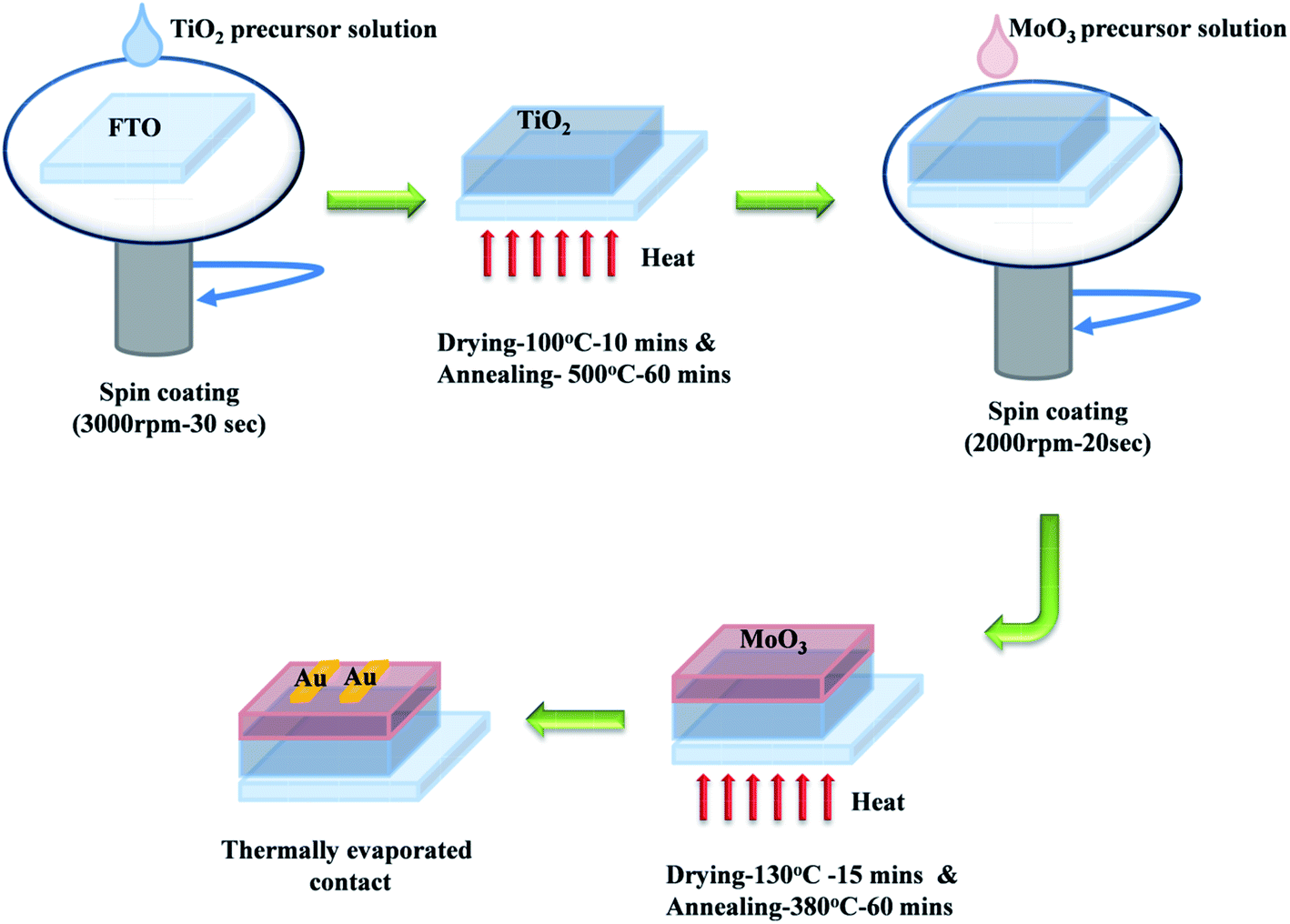 | ||
| Fig. 1 Schematic illustrating the fabrication of a bilayer UV detector device. | ||
X-ray diffraction was carried out using Cu Kα radiation (Powder X-ray Diffractometer, PANalytical, Xpert) with the diffraction angle from 10 to 80°. UV-visible absorption and transmittance studies were carried out using an Agilent Cary UV-visible absorption spectrometer. FE-SEM analysis was carried out with a Quanta FEG 2000. X-ray photoelectron spectroscopy was carried out using a PHI VersaProbe III scanning XPS microprobe, Physical Electronics, USA. Electrochemical impedance spectroscopy with a two-electrode system was carried out using a Zahner Zennium electrochemical workstation in the frequency range from 10 mHz to 100 kHz with an amplitude of 10 mV. I–V and I–t characteristics of the device (active area of 0.24 cm2) were measured using a 2450 Keithley source meter unit. I–V characteristics were measured in the dark, under 1 sun illumination and illumination by a 352 nm UV lamp with an intensity of 76 μW cm−2. I–t characteristics were measured in the dark and under illumination by a 352 nm UV lamp with an intensity of 76 μW cm−2. The spectral response measurements were carried out using a Bentham PVE300 photovoltaic characterization setup with a TMC 300 monochromator.
Results and discussion
XRD analysis was carried out to confirm the crystalline nature of the samples. Fig. S1† shows the XRD patterns of TiO2, MoO3 and TiO2/MoO3 films coated on FTO/glass. The evident peaks of all the films could be matched well with the standard data of anatase-TiO2 (ICSD-98-00-5225) and α-MoO3 (ICSD-98-001-7296) after excluding the peaks of FTO. The grain size was calculated using the Scherrer formula and the mean grain size was 48.14 nm for TiO2, 17.12 nm for MoO3 and 15.17 nm for TiO2/MoO3 film. The changes observed in the grain size can be correlated with the changes in the oxygen vacancy concentration as indicated by the variation in the intensity of the secondary peaks.46,47FE-SEM analysis was carried out to investigate the surface morphology and the obtained images are shown in Fig. 2a–c. The surface of the TiO2 film was observed to have agglomerated irregular spherical nanoparticles. The MoO3 film had a nanospike-like structure on FTO while the structure shown by the TiO2/MoO3 film was not exactly similar. A decrease in the length of nanospikes of MoO3 and densely packed alignment was observed in the case of MoO3 film deposited on TiO2. This may be due to the substrate dependent growth of MoO3 structures. For the bare MoO3 film, the growth was on the smooth film of flat FTO/glass and for the TiO2/MoO3 film, the growth of MoO3 was on the film of agglomerated TiO2 nanoparticles.41,48 The change can also be related to the change in the oxygen vacancy concentration that affects the particle size and shape.49 It's known in the literature that denser ZnO nanostructures show a higher photoresponse50 and analogously, we could predict that the reduction in the length and dense packing of MoO3 nanostructures could lead to an improved photoresponse. The FESEM cross-sectional image (Fig. S2†) of the bilayer film confirms the successive growth of TiO2 (∼300 nm thick) and MoO3 (∼260 nm thick) layers.
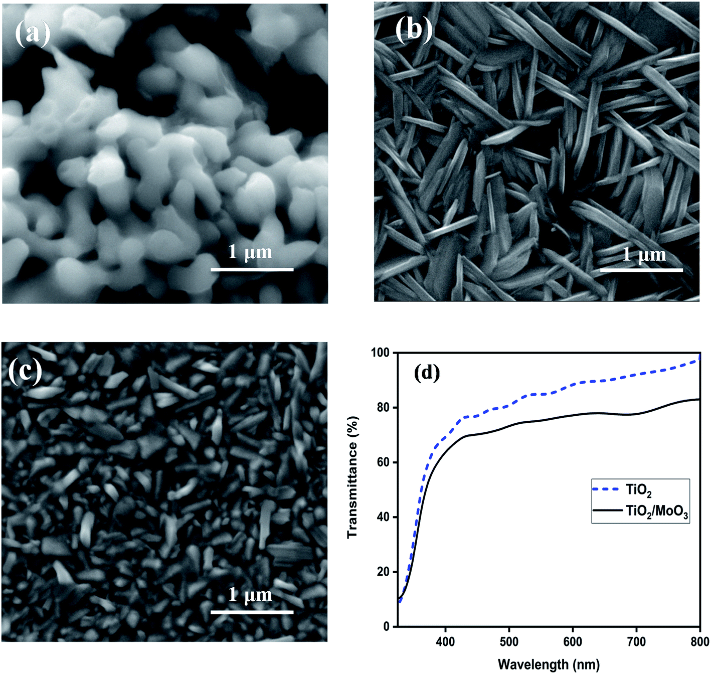 | ||
| Fig. 2 FESEM images of (a) TiO2, (b) MoO3, and (c) TiO2/MoO3 films, and (d) UV-visible transmission spectra of TiO2 and TiO2/MoO3 films. | ||
UV-visible transmission spectra of the films recorded in the wavelength range of 280–800 nm are shown in Fig. 2d. The spectra confirmed that both TiO2 and TiO2/MoO3 films absorb light in the UV region while exhibiting high transparency to the visible light (above 400 nm). The average transmittance of 85% and 74% were observed in the visible region (400–800 nm) for the TiO2 and TiO2/MoO3 films, respectively. It should also be noted that the absorption of light by the bilayer heterojunction film was significantly higher as compared to the TiO2 film (Fig. S3†).
XPS analysis was carried out to confirm the chemical states, as well as the elemental composition of the samples and the results are shown in Fig. 3. The binding energies of Mo 3d3/2 and Mo 3d5/2 for the MoO3 film were located at 236.0 eV and 232.9 eV, respectively, corresponding to the Mo6+ oxidation state.51 These binding energies were shifted to 235.8 eV and 232.7 eV for the Mo 3d in the TiO2/MoO3 film. Though there was a slight shift in Mo 3d binding energies, the oxidation state of Mo6+ remained the same. The binding energy of the O 1s peak in the TiO2/MoO3 heterojunction was located at 530.8 eV which was also shifted downwards by 0.2 eV compared to that of the O 1s peak for MoO3. Both Mo 3d and O 1s peaks of the TiO2/MoO3 film were shifted to lower energies than those of the MoO3 film and this can be attributed to the electron transfer between TiO2 and MoO3 in the heterojunction.25
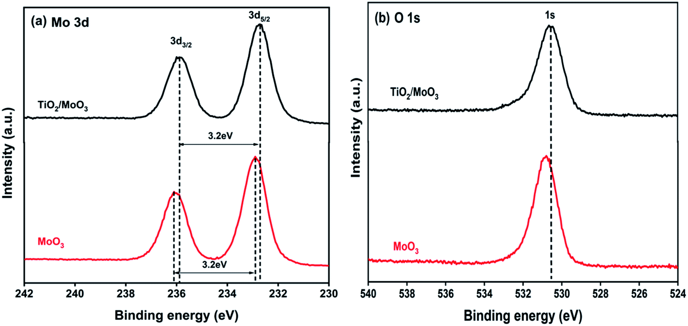 | ||
| Fig. 3 XPS spectra of (a) Mo 3d and (b) O 1s of MoO3 & TiO2/MoO3 films. | ||
Electrochemical impedance spectroscopy was carried out to analyse the charge transfer resistance and separation efficiency of the heterojunction. The spectra were recorded with the back contact FTO and the front contact Au in a 2 electrode configuration at room temperature under dark conditions. The obtained Nyquist plots are shown in Fig. 4a. It was evident from the spectra that the radius of the semicircle for the bilayer heterojunction device was much smaller than that of the single layer device. The small semi-circular arc for the TiO2/MoO3 heterojunction indicated a smaller charge transfer resistance which can be related to the faster charge transfer across the interface. This also corresponds to the higher efficiency of the heterojunction for the separation of carriers.26 The equivalent circuit model used for fitting and the resistance values are given in Fig. S9 and Table S1.†
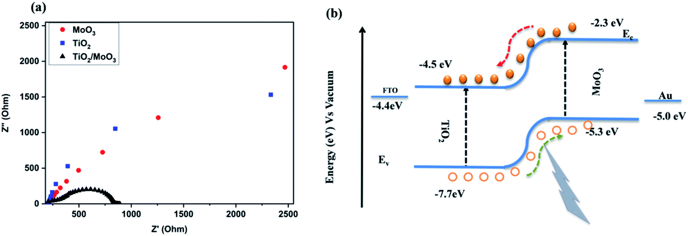 | ||
| Fig. 4 (a) Electrochemical impedance spectra of MoO3, TiO2, and TiO2/MoO3 films, and (b) energy level diagram of the TiO2/MoO3 heterojunction. | ||
To understand the electrical behaviour of the TiO2/MoO3 bilayer, two probe I–V measurements were done in the dark at room temperature with Au and FTO as a front and back contact, respectively, and the results are shown in Fig. 5a. Before the fabrication of the heterojunction, TiO2 and MoO3 were studied separately. The I–V curve of the TiO2 based device exhibited a Schottky behaviour (Fig. S4a†), while the MoO3 based device showed ohmic conduction (Fig. S5†). However, the I–V curve of the bilayer device exhibited a diode-like behaviour. The diode parameters were analyzed using the ideal diode equation52
 | (1) |
 | (2) |
 | (3) |
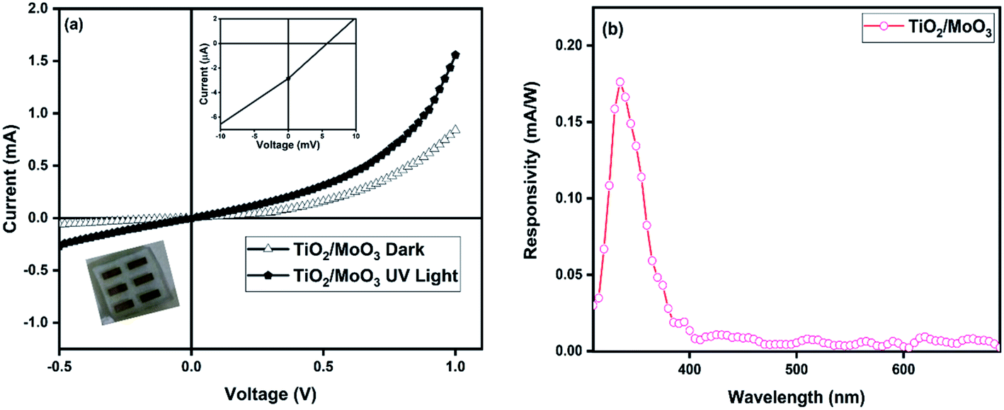 | ||
| Fig. 5 Device characteristics of the bilayer device: (a) I–V characteristics in the dark and under UV illumination, insets: I–V curve under UV light, enlarged around 0 V & a photograph of the device, and (b) spectral responsivity. | ||
The reverse current started increasing slightly at −0.4 V, but the corresponding forward current was one order of magnitude higher which is comparable to the earlier observations with other heterojunction devices.40,54,55 The ideality factor which was greater than unity (2.98) indicates that the charge transport mechanism deviated from the thermionic emission theory applicable for an ideal diode. To further investigate the charge transport mechanism, power-law compliance was considered and the forward I–V data were plotted in a logI–logV scale56 (Fig. S6†). The plot was fitted well with the power-law expression mentioned below with two different slopes.
| I = KVm |
At lower voltages (0.02–0.28 V), the exponent determined was close to unity with a correlation coefficient of 0.99645. This indicates that the current varied linearly with the voltage and the charge transport was governed by Ohm's law. Hence, the thermally generated free electrons were responsible for the current produced at lower bias. Furthermore, an enhancement in the current was observed with the increase in the voltage, indicating that the injected carriers contribute to the rise in current.54,57,58 At higher voltages (0.32–1.0 V), the exponent was determined to be 2.18 with a correlation co-efficient of 0.99589. This indicates that the space charge limited charge transport became pre-dominant, where the number of injected carriers becomes comparable to the thermally generated carriers. The value of the exponent is slightly greater than 2 and this suggests that the injected carriers have just entered into the space charge region.59
I–V characteristics measured under UV light illumination (352 nm) clearly showed the photoconductive nature of the devices. The photocurrent (the difference between the current under UV illumination and dark) of the bilayer device was observed as 1.94 μA at 0 V and it reached a value of 840 μA at a reverse bias of −1 V. The photocurrent without bias was 40 times higher and with bias, it was 3 times higher when compared to that of the single layer TiO2 nanoparticle based device for which the photocurrent was only 42 nA at 0 V and 228 μA at −1 V (Fig. S4†). The devices exhibited photocurrent even under zero bias conditions, due to the photovoltaic effect under UV illumination. The I–V curves enlarged around 0 V showed a photovoltaic behaviour upon UV illumination for both single and bilayer devices (inset in Fig. 4a and S4a†). The TiO2/MoO3 bilayer device showed an open-circuit voltage (Voc) of 5.7 mV and a short-circuit current (Isc) of 2.856 μA, while for the TiO2 single layer, the values of Voc and Isc were 4.4 mV and 0.953 μA, respectively. It can be attributed to the built-in potential at the FTO/TiO2 and TiO2/MoO3 interfaces arising due to alignment of energy bands, which act to separate the photogenerated carriers efficiently.33,60
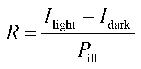
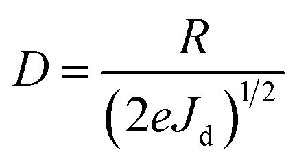
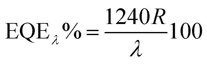
Based on the I–V characteristics, the photoresponsivity (R), detectivity (D) and external quantum efficiency (EQE) were calculated using the formulae mentioned below30
 | (5) |
 | (6) |
where Pill = Iill × A0, Iill is the illumination power density, A0 is the active area, e is the charge of an electron, Jd is the dark current density, R is the photoresponsivity, and λ is the excitation wavelength (352 nm). For the TiO2/MoO3 device, R, D, and EQE were estimated to be 108 mA W−1, 2.26 × 10¹⁰ Jones and 38.04% without bias, while at −1 V bias the values were found to be 46.05 A W−1, 2.84 × 10¹² Jones and 1.62 × 10⁴%, respectively. When compared to the single layer device, the value of R was 40 times higher without bias and 3 times higher with bias. D and EQE were observed to be 1 order higher in magnitude with and without bias.
When the I–V measurements were carried out under 1 sun white light illumination, a negligible photocurrent was observed (Fig. S7†). This confirms that the response was significant only with illumination by UV light of the wavelength corresponding to the bandgap of the film, concurrent with the absorption spectrum. The spectral responsivity measured with 0 V bias (Fig. 5b) has again proven the excellent UV-light detection selectivity of the bilayer heterojunction film, with the highest response shown in the spectral range between 300 and 385 nm. The results confirmed that the device has the ability to work as a visible blind UV detector.
To further understand the self-powering ability, I–t measurements were performed under 0 V bias with an interval of 30 s between UV illuminations (Fig. 6).The photocurrent, rise time and fall time for our bilayer film, as estimated from the I–t characteristics, were found to be 1.94 μA, 1.82 s and 1.42 s, respectively. The high photocurrent upon UV light illumination can be attributed to the photo-desorption of oxygen species on the surface. The dynamics associated with the photo-adsorption/desorption process results in the increase of free carrier density and consequently the photocurrent. The apparent overshoot phenomenon could be related to the charge accumulation at the metal/semiconductor interface.61 It is noteworthy that the time taken to reach the steady state was less than 2 s and the response remained unaltered even after 10 cycles. To understand the photoresponse under external bias, I–t measurements were also performed at −1 V (Fig. S8†). The photocurrent, rise time and fall time were found to be 840 μA, 1.22 s and 1.4 s, respectively. The cycling stability of the device with an applied voltage of −1 V was observed to be slightly inferior, and the dark current was found to increase after 5 cycles. This may be attributed to the redistributed electric field caused by the applied bias, which can induce a decrease in voltage dependent carrier separation and transport.36,62,63
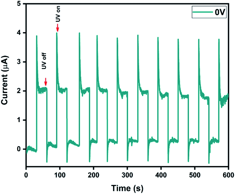 | ||
| Fig. 6 I–t characteristics of the self-powered bilayer device. | ||
However, it's noteworthy that the stability loss observed here was only 5% and there was almost no loss when the device was operated under self-powered mode.
As compared to the literature, our single layer device with the configuration of FTO/TiO2/Au itself showed better performance, under bias conditions lower than the reported ones (Table S3†). The detection capability of the TiO2/MoO3 bilayer device was found to be remarkable in terms of the bias conditions as well as the responsivity when compared with the other reported anatase TiO2 based UV detectors. Also, the rise time is 3 times less and the fall time is 12 times less (Table S4†) when compared to the values reported earlier for the TiO2/MoO3 UV detector.40 This faster response may be attributed to the effective collection of the photogenerated carriers and the consequent recombination loss.68 This corresponds to the effective junction formation between TiO2 and MoO3 layers and the efficient separation of photogenerated carriers.69
It can be seen from Table 1 that the performance of our devices was better when compared with many such reports on TiO2 based self-powered UV detectors. The bilayer device had higher responsivity as well as detectivity at zero bias, even under the relatively weakest illumination. It stands out as the best so far among the devices studied under low light conditions. It is also noteworthy that the photoresponsivity of our self-powered bilayer device at zero bias itself is comparable to that of commercial Si photodetectors (0.1–0.2 A W−1)70 and with a bias of −1 V, it is much higher. However, the slow response speed of the device under 0 V bias was related to the oxygen vacancies.71 The oxygen vacancies produce subgap states and can act as recombination centers. The subgap states hinder carrier excitation upon UV illumination72 and they also act as trap centres to the carriers upon the shut off of UV irradiation, resulting in a slow response.73
| Device | Wavelength (nm) | Intensity of the source (mW cm−2) | Bias (V) | Photoresponsivity (mA W−1) | Detectivity (Jones) | Rise time | Fall time | Ref. |
|---|---|---|---|---|---|---|---|---|
| TiO2/Ag | 350 | 1.2 | 0 | 1.1 | — | 2 ms | 47 ms | 64 |
| TiO2/Ag | 350 | 0.038 | 0 | 32.5 | 6 × 10⁹ | 44 ns | 1.85 μs | 65 |
| NiO/TiO2 | 370 | 0.2 | 0 | 860 | 1.6 × 10¹³ | 3 ms | 60 ms | 60 |
| NiO/TiO2/TiOx | 380 | 0.5 | 0 | 5.66 | 2.5 × 10¹² | <0.1 s | <0.1 s | 39 |
| SnSx/TiO2 | 365 | 2 | 0 | 5.85 | 6.54 × 10¹⁰ | 3 ms | 25 ms | 37 |
| PANI/TiO2 | 320 | 0.87 | 0 | 3.6 | 3.9 × 10¹¹ | 1.2 ms | 22.8 ms | 66 |
| SnO2/TiO2 | 365 | 40 | 0 | 600 | — | 0.02 s | 0.004 s | 38 |
| Au/P3HT/TiO2 | 350 | 1 | 0 | 0.25 | 2.9 × 10¹⁰ | 0.72 s | 0.5 s | 31 |
| ZnO/Ga2O3 | 266 | 1.6 | −0.1 | 9.7 | 2.58 × 10¹² | 100 μs | 900 μs | 67 |
| TiO 2 | 352 | 0.076 | 0 | 2.68 | 3.34 × 10 9 | — | — | This work |
| TiO 2 /MoO 3 | 352 | 0.076 | 0 | 108 | 2.26 × 10 10 | 1.82 s | 1.48 s |
The observed photoresponse is also better than that of most self-powered photodetectors based on various metal oxides such as ZnO, Ga2O3, NiO, and SnO2, which perform under illumination conditions much stronger than ours.60,65,74–77 Overall, the superior performance of the bilayer device, as evident from the discussion above, can be ascribed to the formation of an effective heterojunction between TiO2 and MoO3. The built-in potential at the interface of TiO2/MoO3 leads to an enhanced separation efficiency as well as an effective charge transfer, and enables the device to be self powered.60 The improved and faster response can be related to the reduced recombination. As already mentioned, these improvements could also be due to the morphological factor of having densely aligned nanostructures. It is well known that the adsorption/photodesorption of O2 species upon UV illumination78 followed by the transport of photogenerated carriers79 plays a vital role in UV detection performance. The depletion region would shrink upon application of the reverse bias due to the hole-trapping at the surface. This increases the electron tunneling, and the electron migration in large numbers is related to the EQE over 100%.80,81 It can be proposed that the densely aligned nanostructures could expose multiple junctions sensitive to the UV light and could also provide efficient pathways for the transport of carriers, leading to the enhancement in the photocurrent and EQE.50,82 When compared to previous reports, the improvement can also be related to the mobility of the anatase TiO2 used in this work which is known to be better than that of rutile TiO2.83 Though the densely aligned morphology offers better performance in terms of faster response and high photocurrent, the photocurrent stability with time can be further improved by tuning the surface area.84 There is room for achieving better performance by more carefully optimizing the particle size, morphology, crystallinity, and thickness of the films.
Conclusion
In summary, we have fabricated and studied a fully solution processed transparent TiO2/MoO3 bilayer thin film device with an anatase TiO2 nanoparticle based bottom layer for the first time, for self-powered UV detector application. XPS, electrochemical measurements and current–voltage characteristics of the bilayer have confirmed the formation of an effective heterojunction diode, where the interaction of the energy bands could lead to an efficient charge transfer. The charge transport mechanism of the bilayer device was governed by Ohm's law at low voltages and space charge limited conduction at high voltages. The bilayer device exhibited a very good photoresponsivity and detectivity under 352 nm UV light illumination of very low intensity. The performance was on par with other TiO2 based heterojunctions reported as self-powered UV detectors, showing a photoresponse even under zero bias conditions which was further enhanced at a low bias of −1 V. The self-powered performance of the device was attributed to the built-in potential of the TiO2/MoO3 interface that led to the separation of photogenerated carriers without bias. The improved detection capability exhibited by the TiO2/MoO3 bilayer device in terms of the low bias conditions, high responsivity, high EQE and faster response can be mainly attributed to the better carrier collection as well as the reduced recombination across the heterojunction. The morphological factors of nanostructures and the better mobility of anatase TiO2 nanoparticles could also be the reasons behind the observed enhancement in the performance. The results suggest that the bilayer heterojunction, where the TiO2 nanoparticle film is the platform with the α-MoO3 film on the top, is a promising candidate for self-powered UV detector application with its high transparency as well as the best-in-class photoresponse under low bias and weak illumination conditions.Author contributions
BE carried out all the experiments including synthesis, device fabrication and characterization with initial help from MD. SVB conceptualized the project and supervised the research work. BE and SVB discussed the results, prepared the manuscript and carried out the required revisions.Conflicts of interest
There are no conflicts of interest to declare.Acknowledgements
The authors acknowledge the financial support of SRMIST towards this research work and all the in-campus characterization facilities such as the UV-visible spectrometer at the Department of Physics & Nanotechnology, XPS and FE-SEM facility at NRC and the XRD facility with the support from MNRE (Project No. 31/03/2014-15/PVSE-R&D), Govt. of India. We thank Dr S. Harinipriya and coworkers for the help with the access to electrochemical impedance measurements. We also thank Dr P. Malar and coworkers for the help with the use of a thermal evaporator. We thank Prof. B. Neppolian and coworkers for the access to the EQE facility supported by Department of Science and Technology – Solar Energy Research Initiative (DST; SERB), File No. DST/SERI/FR/2016/S170. We would also like to acknowledge the research grants from DST-SERB [File. No. (ECR/2015/000513)] and MNRE [File. No. 31/03/2014-15/PVSE-R&D], Govt. of India.References
- K. D. Leedy, M. Higashiwaki, R. L. Peterson and S. James, APL Mater., 2019, 7, 022201 CrossRef.
- H. Ohta, M. Hirano, K. Nakahara, H. Maruta, T. Tanabe, M. Kamiya, T. Kamiya and H. Hosono, Appl. Phys. Lett., 2003, 83, 1029–1031 CrossRef CAS.
- C. C Shih, W. Y. Lee, Y. C. Chiu, H. W. Hsu, H. C. Chang, C. L. Liu and W. C. Chen, Sci. Rep., 2016, 6, 20129 CrossRef.
- Z. Q. Zheng, J. D. Yao, B. Wang and G. W. Yang, Sci. Rep., 2015, 5, 11070 CrossRef CAS.
- M. Pavan, S. Rühle, A. Ginsburg, D. A. Keller, H. N. Barad, P. M. Sberna, D. Nunes, R. Martins, A. Y. Anderson, A. Zaban and E. Fortunato, Sol. Energy Mater. Sol. Cells, 2015, 132, 549–556 CrossRef CAS.
- L. Ahtapodov, B. Fimland, K. Kishino and H. Weman, Nano Lett., 2019, 19, 1649–1658 CrossRef.
- S. Abbas, D. Ban and J. Kim, Sens. Actuators, A, 2019, 293, 215–221 CrossRef CAS.
- J. Chen, Z. Li, F. Ni, W. Ouyang and X. Fang, Mater. Horiz., 2020, 7, 1828–1833 RSC.
- C. C. Forin, M. Purica, E. Budianu and P. Schiopu, Proc. Int. Semicond. Conf. CAS, 2012, 1, 131–134 CAS.
- Z. Li, M. K. Joshi, J. Chen, Z. Zhang, Z. Li and X. Fang, Adv. Funct. Mater., 2020, 30, 2005291 CrossRef CAS.
- G. S. Mital and T. Manoj, Chin. Sci. Bull., 2011, 56, 1639–1657 CrossRef.
- X. Chen and S. S. Mao, Chem. Rev., 2007, 107, 2891–2959 CrossRef CAS.
- M. Quintana, T. Edvinsson, A. Hagfeldt and G. Boschloo, J. Phys. Chem. C, 2007, 111, 1035–1041 CrossRef CAS.
- J. Sobuś, G. Burdziński, J. Karolczak, J. Idígoras, J. A. Anta and M. Ziółek, Langmuir, 2014, 30, 2505–2512 CrossRef.
- T. Ling, J. G. Song, X. Y. Chen, J. Yang, S. Z. Qiao and X. W. Du, J. Alloys Compd., 2013, 546, 307–313 CrossRef CAS.
- D. Friedmann, C. Mendive and D. Bahnemann, Appl. Catal., B, 2010, 99, 398–406 CrossRef CAS.
- B. Liu, X. Zhao, J. Yu, I. P. Parkin and A. Fujishima, J. Photochem. Photobiol., C, 2019, 39, 1–57 CrossRef CAS.
- S. Mishra, P. Yogi, P. R. Sagdeo and R. Kumar, ACS Appl. Energy Mater., 2018, 1, 790–798 CrossRef CAS.
- Y. Li, C. Cai, Y. Gu, W. Cheng, W. Xiong and C. Zhao, Appl. Surf. Sci., 2017, 414, 34–40 CrossRef CAS.
- M. Sun, J. Hu, C. Zhai, M. Zhu and J. Pan, Electrochim. Acta, 2017, 245, 863–871 CrossRef CAS.
- I. A. De Castro, R. S. Datta, J. Z. Ou and A. Castellanos-gomez, Adv. Mater., 2017, 29, 1701619 CrossRef.
- D. Kwak, M. Wang, K. J. Koski, L. Zhang, H. Sokol, R. Maric and Y. Lei, ACS Appl. Mater. Interfaces, 2019, 11, 10697–10706 CrossRef CAS.
- S. Sonu, V. Dutta, S. Sharma, P. Raizada, A. Hosseini-Bandegharaei, V. Kumar Gupta and P. Singh, J. Saudi Chem. Soc., 2019, 23, 1119–1136 CrossRef.
- W. Yang, K. Hu, F. Teng, J. Weng, Y. Zhang and X. Fang, Nano Lett., 2018, 18, 4697–4703 CrossRef CAS.
- M. Lu, C. Shao, K. Wang, N. Lu, X. Zhang, P. Zhang, M. Zhang, X. Li and Y. Liu, ACS Appl. Mater. Interfaces, 2014, 6, 9004–9012 CrossRef CAS.
- S. Sun, X. Liao, X. Pu, Y. Sun, G. Yin, Y. Yao, Z. Huang and X. Pu, RSC Adv., 2017, 7, 22983–22989 RSC.
- S. Paek, J. Kang, H. Jung, S. Hwang and J. Choy, Chem. Commun., 2009, 48, 7536–7538 RSC.
- N. K. Shrestha, Y. Nah and P. Schmuki, Chem. Commun., 2009, 15, 2008–2010 RSC.
- Q. Chen, Y. Zhang, T. Zheng, Z. Liu, L. Wu, Z. Wang and J. Li, Nanoscale Adv., 2020, 2, 2705–2712 RSC.
- M. Moun, M. Kumar, M. Garg, R. Pathak and R. Singh, Sci. Rep., 2018, 1, 1–10 Search PubMed.
- L. Zheng, X. Deng, Y. Wang, J. Chen, X. Fang, L. Wang, X. Shi and H. Zheng, Adv. Funct. Mater., 2020, 30, 2001604 CrossRef CAS.
- X. Li, S. Gao, G. Wang, Z. Xu, S. Jiao, D. Wang, Y. Huang, D. Sang, J. Wang and Y. Zhang, J. Mater. Chem. C, 2020, 8, 1353–1358 RSC.
- Y. Shen, X. Yan, Z. Bai, X. Zheng, Y. Sun, Y. Liu, P. Lin, X. Chen and Y. Zhang, RSC Adv., 2015, 5, 5976–5981 RSC.
- J. Xing, H. Wei, E. J. Guo and F. Yang, J. Phys. D: Appl. Phys., 2011, 44, 375104 CrossRef.
- A. M. Selman and Z. Hassan, Superlattices Microstruct., 2015, 83, 549–564 CrossRef CAS.
- D. Zhang, C. Liu, B. Yin, R. Xu, J. Zhou, X. Zhang and S. Ruan, Nanoscale, 2017, 9, 9095–9103 RSC.
- J. Chen, J. Xu, S. Shi, R. Cao and D. Liu, ACS Appl. Mater. Interfaces, 2020, 12, 23145–23154 CrossRef CAS.
- C. Gao, X. Li, X. Zhu, L. Chen, Y. Wang, F. Teng, Z. Zhang, H. Duan and E. Xie, J. Alloys Compd., 2014, 616, 510–515 CrossRef CAS.
- Y. Gao, J. Xu, S. Shi, H. Dong, Y. Cheng, C. Wei, X. Zhang, S. Yin and L. Li, ACS Appl. Mater. Interfaces, 2018, 10, 11269–11279 CrossRef CAS.
- B. Yin, Y. Zhang, K. Li, J. Zhou, C. Liu, M. Zhang and S. Ruan, Nanotechnology, 2019, 30, 465501 CrossRef CAS.
- T. Zhai and J. Yao, One-dimensional nanostructures: principles and applications, Wiley&Sons, United States, 2012 Search PubMed.
- P. Gao, H. Wang, Z. Sun, W. Han, J. Li and J. Ye, Appl. Phys. Lett., 2013, 103, 213505 CrossRef.
- J. Szlufcik, J. Majewski, A. Buczkowski, J. Radojewski, L. Jȩdral and E. B. Radojewska, Sol. Energy Mater., 1989, 18, 241–252 CrossRef CAS.
- M. Sasani Ghamsari and A. R. Bahramian, Mater. Lett., 2008, 62, 361–364 CrossRef CAS.
- S. Murase and Y. Yang, Adv. Mater., 2012, 24, 2459–2462 CrossRef CAS.
- R. Parra, C. M. Aldao, J. A. Varela and M. S. Castro, J. Electroceram., 2005, 14, 149–156 CrossRef CAS.
- S. Aškrabia
![[c with combining umlaut]](https://www.rsc.org/images/entities/char_0063_0308.gif) , Z. Dohčevia-Mitrovia, A. Kremenovia, N. Lazarevia, V. Kahlenberg and Z. V. Popovia, J. Raman Spectrosc., 2012, 43, 76–81 CrossRef.
, Z. Dohčevia-Mitrovia, A. Kremenovia, N. Lazarevia, V. Kahlenberg and Z. V. Popovia, J. Raman Spectrosc., 2012, 43, 76–81 CrossRef. - J. Song and S. Lim, J. Phys. Chem. C, 2007, 111, 596–600 CrossRef CAS.
- R. Mehmood, X. Wang, P. Koshy, J. L. Yang and C. C. Sorrell, CrystEngComm, 2018, 20, 1536–1545 RSC.
- V. Postica, M. Hoppe, J. Grottrup, P. Hayes, V. Robisch, D. Smazna, R. Adelung, B. Viana, P. Aschehoug, T. Pauporté and O. Lupan, Solid State Sci., 2017, 71, 75–86 CrossRef CAS.
- S. Xie, D. Cao, Y. She, H. Wang, J. W. Shi, M. K. Leung and C. Niu, Chem. Commun., 2018, 54, 7782–7785 RSC.
- D. K. Schroder, Semiconductor Material and Device Characterization, Wiley&Sons, United States, 2015 Search PubMed.
- H. Ã. Altuntas, A. Bengi, U. Aydemir, T. Asar, S. S. Cetin, I. Kars, S. Altindal and S. Ozcelik, Mater. Sci. Semicond. Process., 2009, 12, 224–232 CrossRef CAS.
- P. C. Ramamurthy, W. R. Harrell, R. V. Gregory, B. Sadanadan and A. M. Rao, Polym. Eng. Sci., 2004, 44, 28–33 CrossRef CAS.
- P. Singh, P. K. Rout, H. Pandey and A. Dogra, J. Mater. Sci., 2018, 53, 4806–4813 CrossRef CAS.
- H. Elangovan, A. V. Kesavan, K. Chattopadhyay and P. C. Ramamurthy, J. Appl. Phys., 2019, 125, 245302 CrossRef.
- A. Wahl and J. Augustynski, J. Phys. Chem. B, 1998, 5647, 7820–7828 CrossRef.
- M. A. Lampert and R. B. Schilling, in Semiconductors and Semimetals, ed. R. K. Williardson and A. Beer, Elsevier, Amsterdam, 1970, vol. 6, ch. 1, pp. 1–96 Search PubMed.
- X. Qiao, J. Chen and D. Ma, J. Phys. D: Appl. Phys., 2010, 43, 215402 CrossRef.
- R. Cao, J. P. Xu, S. Shi, J. Chen, D. Liu, Y. Bu, X. S. Zhang, S. Yin and L. Li, J. Mater. Chem. C, 2020, 8, 9646–9654 RSC.
- Y. Fang, Y. Hou, Y. Hu and F. Teng, Materials, 2015, 8, 4050–4060 CrossRef CAS.
- W. P. Dumke, Appl. Phys. Lett., 1967, 11, 314–316 CrossRef.
- S. Luryi in Hot Electrons in Semiconductors, ed. N.Balkan, Clarendon Press, Oxford, 1998, vol. 6, ch. 17, pp. 389–395 Search PubMed.
- J. Xu, W. Yang, H. Chen, L. Zheng, M. Hu, Y. Li and X. Fang, J. Mater. Chem. C, 2018, 6, 3334–3340 RSC.
- H. Fang, C. Zheng, L. Wu, Y. Li, J. Cai, M. Hu, X. Fang, R. Ma, Q. Wang and H. Wang, Adv. Funct. Mater., 2019, 29, 1809013 CrossRef.
- L. Zheng, P. Yu, K. Hu, F. Teng, H. Chen and X. Fang, ACS Appl. Mater. Interfaces, 2016, 8, 33924–33932 CrossRef CAS.
- B. Zhao, W. Fei, C. Hongyu, Z. Lingxia, S. Longxing, Z. Dongxu and X. Fang., Adv. Funct. Mater., 2017, 27, 1700264 CrossRef.
- S. Li, Y. Zhang, W. Yang, H. Liu and X. Fang, Adv. Mater., 2020, 32, 1905443 CrossRef CAS.
- M. Razeghi and A. Rogalski, J. Appl. Phys., 1996, 79, 7433–7473 CrossRef CAS.
- W. Zheng, X. Li, C. Dong, X. Yan and G. He, RSC Adv., 2014, 4, 44868–44871 RSC.
- P. Ivanoff Reyes, C. J. Ku, Z. Duan, Y. Xu, E. Garfunkel and Y. Lu, Appl. Phys. Lett., 2012, 101, 2010–2014 CrossRef.
- K. Y. Chen, S. P. Chang and C. hung Lin, RSC Adv., 2019, 9, 87–90 RSC.
- Q. Chen, H. Ding, Y. Wu, M. Sui, W. Lu, B. Wang, W. Su, Z. Cui and L. Chen, Nanoscale, 2013, 5, 4162–4165 RSC.
- J. Chen, W. Ouyang, W. Yang, J. H. He and X. Fang, Adv. Funct. Mater., 2020, 30, 1909909 CrossRef CAS.
- Y. Wang, C. Wu, D. Guo, P. Li, S. Wang, A. Liu, C. Li, F. Wu and W. Tang, ACS Appl. Electron. Mater., 2020, 2, 2032–2038 CrossRef CAS.
- Y. Wang, L. Li, H. Wang, L. Su, H. Chen, W. Bian, J. Ma, B. Li, Z. Liu and A. Shen, Nanoscale, 2020, 12, 1406–1413 RSC.
- B. Deka Boruah, Nanoscale Adv., 2019, 1, 2059–2085 RSC.
- D. Gedamu, I. Paulowicz, S. Kaps, O. Lupan, S. Wille, G. Haidarschin, Y. K. Mishra and R. Adelung, Adv. Mater., 2014, 26, 1541–1550 CrossRef CAS.
- Y. K. Mishra, G. Modi, V. Cretu, V. Postica, O. Lupan, T. Reimer, I. Paulowicz, V. Hrkac, W. Benecke, L. Kienle and R. Adelung, ACS Appl. Mater. Interfaces, 2015, 7, 14303–14316 CrossRef CAS.
- S. Dhar, T. Majumder and S. P. Mondal, ACS Appl. Mater. Interfaces, 2016, 8, 31822 CrossRef CAS; W. Yin, J. Yang, K. Zhao, A. Cui, J. Zhou, W. Tian, W. Li, Z. Hu and J. Chu, ACS Appl. Mater. Interfaces, 2020, 12, 11797–11805 CrossRef.
- W. Yin, J. Yang, K. Zhao, A. Cui, J. Zhou, W. Tian, W. Li, Z. Hu and J. Chu, ACS Appl. Mater. Interfaces, 2020, 12, 11797–11805 CrossRef CAS.
- V. Postica, I. Paulowicz, O. Lupan, F. Schütt, N. Wol and A. Cojocaru, Vacuum, 2019, 166, 393–398 CrossRef CAS.
- Y. Li, W. Xie, X. Hu, G. Shen, X. Zhou, Y. Xiang, X. Zhao and P. Fang, Langmuir, 2010, 26, 591–597 CrossRef CAS.
- R. Gottesman, A. Song, I. Levine, M. Krause, A. T. M. N. Islam, D. Abou-Ras, T. Dittrich, R. Van de Krol and A. C. Chemseddine, Adv. Funct. Mater., 2020, 30, 1910832 CrossRef CAS.
Footnotes |
| † Electronic supplementary information (ESI) available: XRD patterns of TiO2, MoO3 and TiO2/MoO3 films; FE-SEM cross-sectional image of the bilayer film; UV absorption spectra; I–V and I–t characteristics of the TiO2 single layer device; I–V characteristics of the MoO3 single layer device, logI–logV plot of the bilayer device; equivalent circuit model for EIS; table comparing the resistance values of TiO2, MoO3 and TiO2/MoO3 films as calculated using the EIS equivalent circuit model; calculated diode parameters of the bilayer device; table comparing the performance of TiO2 based UV detectors; table comparing the performance of TiO2/MoO3 based UV detectors; statistical data on the performance of the bilayer device based on the 34 devices made. See DOI: 10.1039/d0na00780c |
| ‡ Current address: Department of Physics, SRM Institute of Science and Technology, Ramapuram, Chennai-600089. |
| This journal is © The Royal Society of Chemistry 2021 |