
 Open Access Article
 This Open Access Article is licensed under a Creative Commons Attribution-Non Commercial 3.0 Unported Licence
Second-harmonic generation enhancement in monolayer transition-metal dichalcogenides by using an epsilon-near-zero substrate†
Pilar G.
Vianna
 ,
Aline dos S.
Almeida
,
Rodrigo M.
Gerosa
,
Dario A.
Bahamon
and
Christiano J. S.
de Matos
*
,
Aline dos S.
Almeida
,
Rodrigo M.
Gerosa
,
Dario A.
Bahamon
and
Christiano J. S.
de Matos
*
MackGraphe – Graphene and Nanomaterials Research Institute, Mackenzie Presbyterian University, São Paulo – 01302-907, Brazil. E-mail: cjsdematos@mackenzie.br
First published on 13th November 2020
Abstract
Monolayer transition-metal dichalcogenides (TMDCs) present high second-order optical nonlinearity, which is extremely desirable for, e.g., frequency conversion in nonlinear photonic devices. On the other hand, the atomic thickness of 2D materials naturally leads to low frequency converted intensities, highlighting the importance of designing structures that enhance the nonlinear response for practical applications. A number of methods to increase the pump electric field at 2D materials have been reported, relying on complex plasmonic and/or metasurface structures. Here, we take advantage of the fact that unstructured substrates with a low refractive index naturally maximize the pump field at a dielectric interface, offering a simple means to promote enhanced nonlinear optical effects. In particular, we measured second harmonic generation (SHG) in MoS2 and WS2 on fluorine tin oxide (FTO), which presents an epsilon-near zero point near our 1550 nm pump wavelength. Polarized SHG measurements reveal an SHG intensity that is one order of magnitude higher on FTO than on a glass substrate.
Introduction
Much recent attention has been paid to the nonlinear optical response in 2D materials, which are anticipated to provide innovative approaches to enable devices such as all-optical modulators, saturable absorbers, THz wave generators, wavelength converters, optical polarizers, optical sensors and optical limiters.1,2 All the mentioned devices suggest applications with new functionalities, high performance, and reduced integration complexity for photonic and optoelectronic platforms.3,42D materials have been shown to exhibit extremely high nonlinear optical susceptibilities, with several nonlinear optical effects observed, including second5–10 and third9,11,12 harmonic generation (SHG/THG), sum-frequency generation,13 four-wave mixing,13–15 and high-harmonic generation.16–18 This makes frequency conversion in 2D materials extremely promising, with potential applications in ultrafast pulse characterization,19 all-optical wavelength conversion for telecommunications,4 optical imaging,7,13 quantum information processing,20,21 and nanoscale lightsources,22,23 among others. In addition, SHG and THG have proven to be a key technique for crystal orientation and characterization of fundamental material properties.12,24
In particular, transition-metal dichalcogenide (TMDC) monolayers, such as molybdenum disulfide (MoS2) and tungsten disulfide (WS2), are non-centrosymmetric and present a high second order nonlinear optical susceptibility,5,9 essential for frequency conversion applications based on second-order nonlinear effects. However, direct TMDC utilization for nonlinear optical applications is still an ongoing challenge due to the atomic thickness of 2D materials and, thus, reduced light–matter interaction, which naturally leads to low net frequency converted intensities. Thus, ways to enhance the process and maximize the nonlinear interaction are crucial for making practical applications viable.
Several strategies have been designed to enhance the nonlinear optical SHG process in TMDCs and other 2D materials, such as excitation near excitonic resonances,25–28 including experiments carried out at low temperature29 and with electrostatic doping.30 Another promising class of methods is the combination of 2D materials with different field-enhancement platforms, including plasmonic nanostructures for localized surface plasmon excitation,31–35 hybrid dielectric structures,36,37 metallic and dielectric metasurfaces governed by bound states in the continuum,38–42 photonic crystal nanocavities,43,44 optical microcavities45,46 and waveguides.47
Although these methods have been proven to enhance the SHG fields, complex and time-consuming fabrication processes are required. Plasmonic metal nanostructures, for example, require that the fundamental or the frequency-converted field be overlapped with the resonance spectrum of the nanostructures, thus demanding specific nanofabrication techniques to appropriately tune the plasmon resonance.36 Also, it is well known that noble metal structures exhibit strong optical loss in the visible band, which greatly influences the nonlinear response.35,48 Metasurfaces, in turn, demand high resolution and often require fabrication by electron-beam lithography, imposing scalability and cost drawbacks in practical manufacturing of nonlinear devices. The same applies to photonic crystal nanocavities, which rely on high definition lithographic methods, essential for the design of superior quality resonance structures in which mode coupling is required.43,44 In the case of optical microcavities and waveguides, precise coupling, phase matching and dispersion management are required, thus, adding complexity to practical applications.
A simpler approach to field-enhancement, however, seems to have been so far virtually overlooked. It consists of acknowledging that, as the 2D material lies at the interface between two dielectrics, the pump field on it is given by the electromagnetic boundary conditions that arise from the reflection and refraction phenomena. In particular, for a regular material (i.e., not a metamaterial) substrate, the field will be maximum if the refractive index tends to zero. The impact of a low refractive index, at the pump frequency, can be appreciated from the expression for the second-harmonic intensity, which can be derived using the nonlinear optical sheet susceptibility formalism and that at normal incidence is given by:49
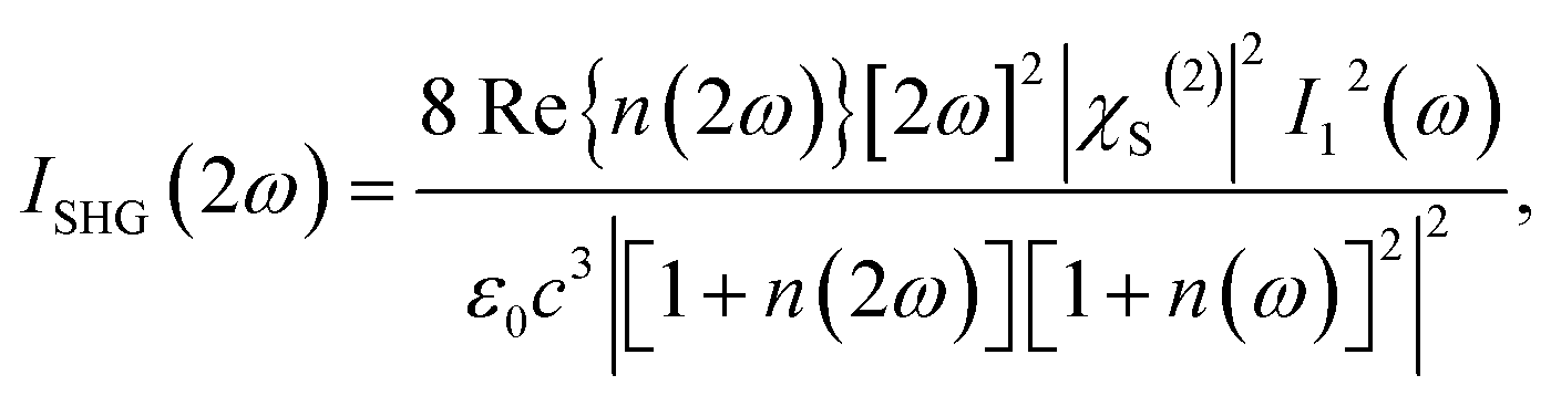 | (1) |
Here, to increase the nonlinear frequency conversion efficiency in mechanically exfoliated monolayer TMDCs, we propose and demonstrate the use of substrates presenting an epsilon-near-zero point close to the pump wavelength. Fluorine tin oxide (FTO) is used as the substrate with the ENZ point close to the 1550 nm telecommunication spectral range, and MoS2 and WS2 are used as the monolayer 2D materials. Polarized SHG measurements were performed and we observed an SHG intensity 7.6 ± 2.1 times greater for MoS2 and 8.2 ± 2.8 times greater for WS2 on the FTO substrate than that for the same materials on glass, which was found to be compatible with our theoretical predictions.
Results and discussion
Theoretical modelling and SHG enhancement factor
Theoretical modeling of SHG was planned to reflect the experimental conditions, described later in this manuscript, in which a monolayer TMDC is deposited onto an FTO film supported by glass. Fig. 1A shows the dielectric function of FTO, modeled by using the Drude free electron model with parameters obtained by fitting experimental transmission spectra (see Methods and the ESI†). The ENZ point is expected to be around ∼1760 nm. Using the obtained dielectric function, we first calculate the SHG fields generated by MoS2 on the FTO substrate using Green's function formalism54 in conjunction with the vacuum interface model55,56 and the transfer matrix method. We use a variable FTO thickness, as well as the dielectric function of SiO2 available in ref. 57 for the supporting soda lime glass. The SHG fields above and below the monolayer MoS2 are calculated and then propagated through the different layers using the transfer matrix method (see Methods and the ESI†). In this way, the total transmitted SHG field was obtained.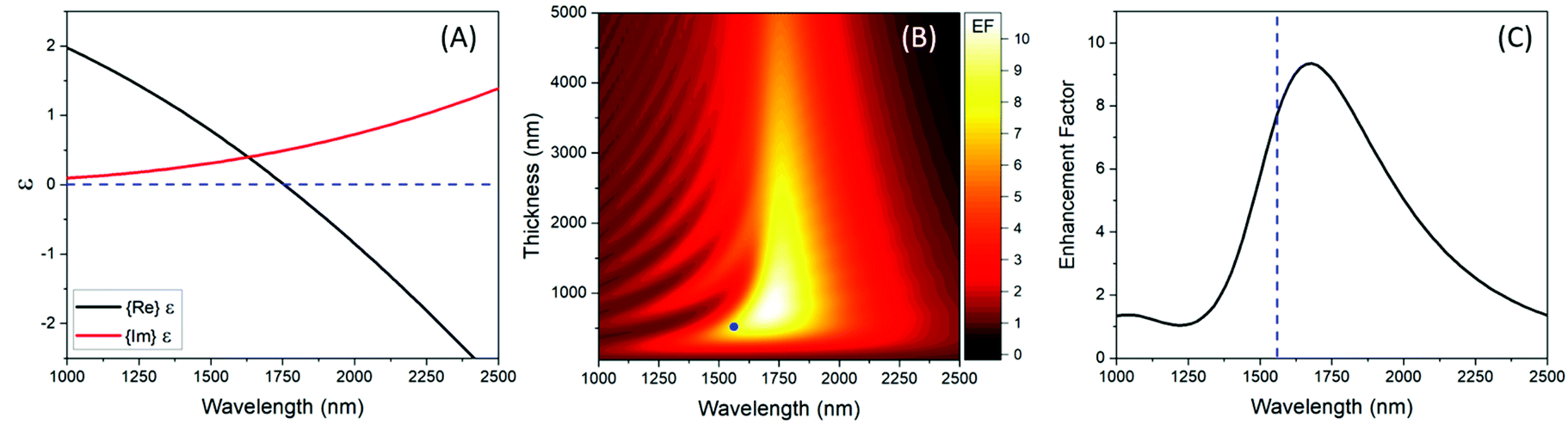 | ||
| Fig. 1 (A) Dielectric function of FTO. (B) Enhancement factor as a function of wavelength for varying thicknesses of the FTO-on-glass substrate. Blue dot indicates the experimental conditions. (C) Theoretical SHG enhancement factor as a function of wavelength for a 520 nm FTO thickness. Dashed line shows the experimental wavelength. | ||
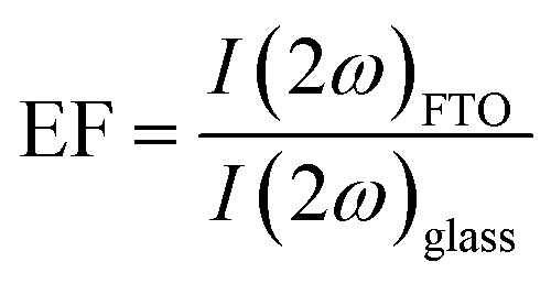
For a direct comparison of the SHG on a standard substrate, we normalized the intensity of the SHG on FTO by the intensity of the SHG on glass (see the ESI†), which we define as the SHG enhancement factor (EF):
 | (2) |
Fig. 1B shows the EF as a function of wavelength for different FTO thicknesses. It is possible to observe that the SHG intensity varies with the substrate thickness, due to interferometric effects, and excitation wavelength, achieving a maximum EF of 10.68 at 1720 nm wavelength for a 770 nm-thick substrate. Fig. 1C shows the EF as a function of the pump wavelength for our experimental substrate (520 nm thickness), represented by the blue circle in Fig. 1B. For our pump, at 1560 nm, represented by the blue dashed line in Fig. 1C, the SHG on FTO is ∼7.7 times more intense than that on glass. The largest enhancement factor, of ∼9.3, is observed at 1680 nm, for the 520 nm thickness.
Experiments
Experimentally, monolayer MoS2 and WS2 were obtained by mechanical exfoliation and transferred to the surfaces of FTO, with 520 nm thickness on glass, and plain glass (for comparison) (for additional details, see Methods). Flake characterization was performed by Raman spectroscopy (WITec Alpha 300R) with excitation at 532 nm (see the ESI†). To minimize possible substrate thickness/roughness variations, MoS2 and WS2 flakes were transferred to the same FTO substrate (see Fig. S7 in the ESI†). The glass used as the substrate in the reference experiments was the same as the one used for FTO deposition.Nonlinear optical measurements consisted of SHG. The experimental setup can be seen in Fig. 2 and included a 1560 nm mode-locked Er-doped fiber laser (FFS, Toptica Photonics) with an 89 MHz repetition rate and 150 fs pulse duration, used as the pump. The laser was focused on the sample at normal incidence with a 20× objective lens, leading to a ∼3 μm focused beam diameter. Using a pair of 5× objective lenses, the SHG signal at 785 nm was collected by transmission and directed to a spectrometer equipped with an iDus Si CCD detector. The detector presents no quantum efficiency at 1560 nm and the remnant pump power was kept low after the sample to avoid any possible damage to the spectrometer. The spectrometer's grating and settings, set to measure the SHG and THG wavelengths, did not direct the pump radiation to the detector. Therefore, the pump generated no features in the spectrum and no filter was needed for blocking the laser before signal collection. Polarized SHG measurements were performed using a linear polarizer (for the pump) and an analyzer (for the SHG signal) in motorized rotation stages. A quarterwave plate adjusted the pump polarization to be circular, so that rotating the polarizer led to minimal intensity changes. A light source, a CCD camera and some optics were used to optically image, in reflection, the monolayer flakes and the THG signal (at 520 nm), with the latter indicating the pump beam position (see the ESI† for additional details). The pump average power was kept at 10 mW to avoid the damage of the monolayer TMDs. Measurements were performed with the analyzer parallel and perpendicular to the incident light polarization.
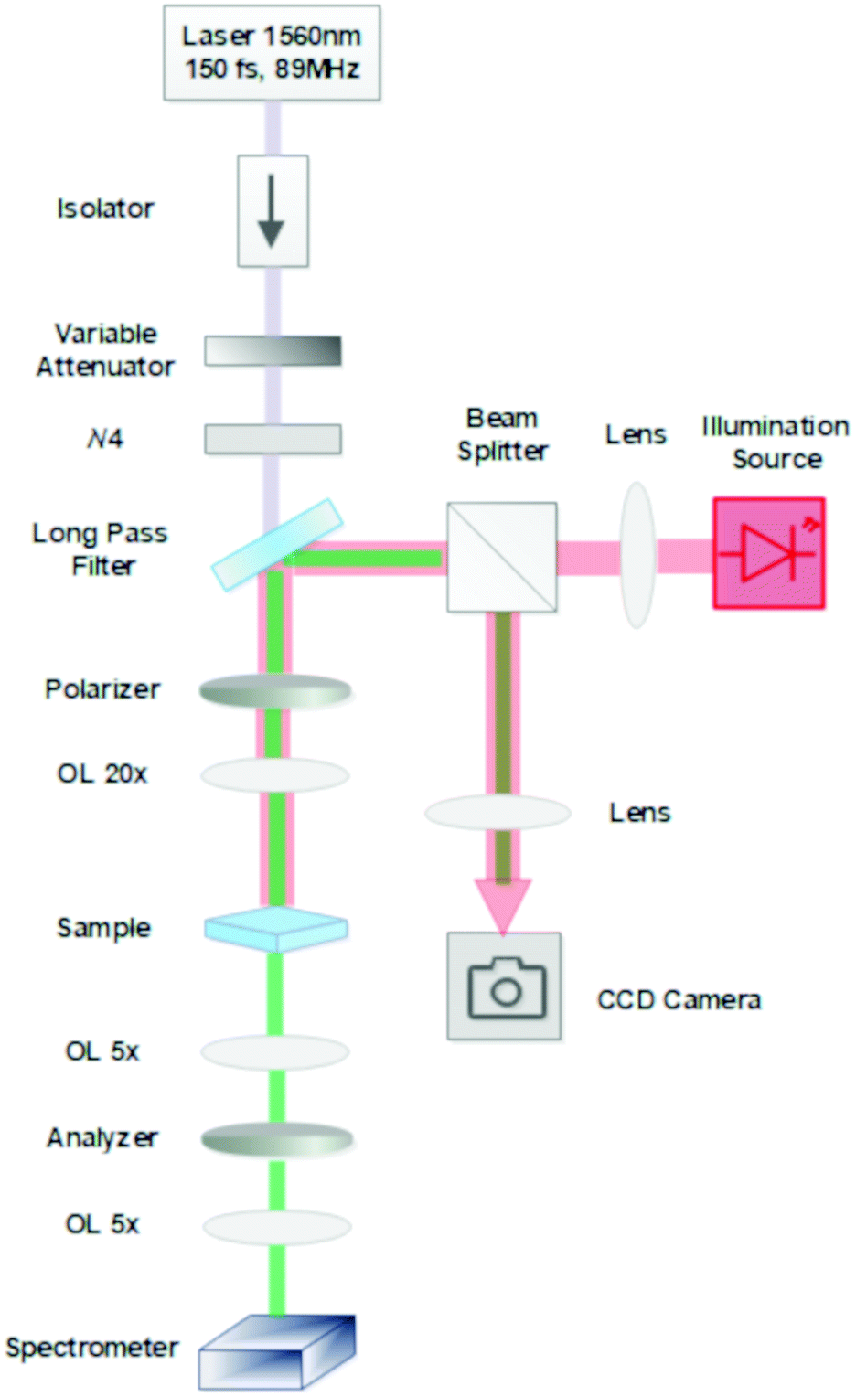 | ||
| Fig. 2 Experimental setup for SHG characterization of the samples. | ||
For polarization-resolved measurements, the two motorized stages, containing the polarizer and the analyzer, were rotated with 5° steps, yielding 73 SHG spectra measured from 0° to 360°. Data for MoS2 on FTO and MoS2 on glass were acquired on the same day to minimize system induced intensity fluctuations, and the standard deviation of at least 10 measurements was used for error estimates. Spectra were obtained with 2 s integration time and 2 accumulations. Each spectrum was individually analyzed and the SHG intensity values were calculated from the integral of each spectrum.
The SHG intensity dependence on the polarization angle can be seen in Fig. 3, for the parallel pump–SHG polarization configuration. The curves for bare FTO, MoS2/FTO and WS2/FTO samples are shown in black, red and blue, respectively. All data were normalized by the MoS2/glass maximum SHG intensity. The maximum normalized SHG intensities were found to be 29.3, 13.3 and 5.6 for WS2/FTO, MoS2/FTO and FTO respectively. It is important to note that FTO presented a relatively strong SHG component, which can only be observed in the parallel polarization configuration. This FTO SHG component is possibly the evidence of some substrate local remnant (and variable) crystallinity,58 even though the film was produced by sputtering (see Methods), which tends to yield an amorphous material. This component is not uniform along the substrate and interferes with the TMDC SHG signal, resulting in distorted SHG patterns in the parallel configuration as shown in Fig. 3, and making it difficult to separate the substrate and the 2D material contributions (see the ESI†). Without the substrate's interference, the SHG signal in monolayer TMDCs is expected to exhibit the typical sinusoidal dependence on the polarization angle, with a 60° period, compatible with the hexagonal symmetry and point group D3h.4,10 It is important to emphasize that the FTO SHG component is only observed in the parallel configuration, and for that reason, our analysis mainly focuses on the SHG obtained with the perpendicular pump–SHG polarization configuration, which eliminates the FTO interfering signal.
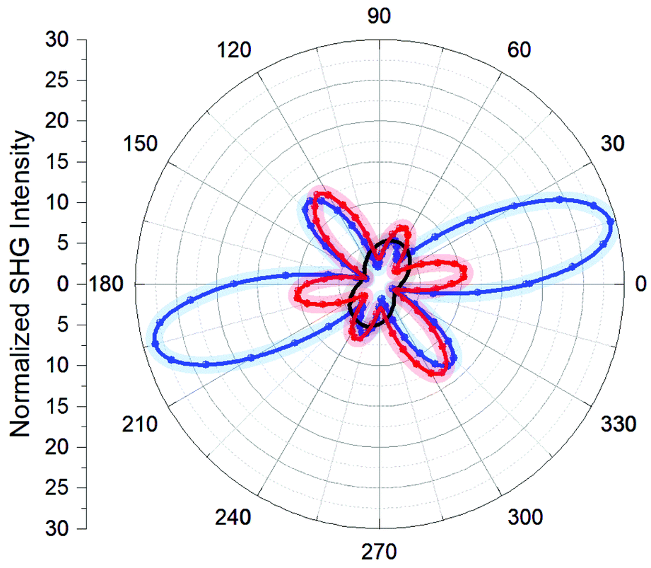 | ||
| Fig. 3 Experimental SHG intensity as a function of pump polarization angle in the parallel polarization configuration for FTO (black), MoS2/FTO (red) and WS2/FTO (blue), normalized by the maximum measured SHG signal on the MoS2/glass sample. | ||
In Fig. 4, the polarized SHG measurements for the perpendicular pump–SHG polarization configuration can be observed for both the TMDCs on FTO and on glass. The intensity values were again normalized by the maximum SHG intensity obtained with MoS2 on glass. Fig. 4A presents the experimental results for MoS2, with the red (black) curve representing results for the FTO (glass) substrate. The SHG intensity is 7.6 ± 2.1 times larger for the material deposited on FTO than that for the monolayer on glass, agreeing with theoretical predictions. The polarization-dependent SHG profile for MoS2 in the perpendicular configuration presents the characteristic sinusoidal behaviour with a 60° period, as expected for monolayer MoS2 (see the ESI† for theoretical prediction). MoS2/glass and WS2/glass in the parallel configuration present the same pattern and intensity as their counterparts in the perpendicular configuration, only with a 30° phase shift (see the ESI†).
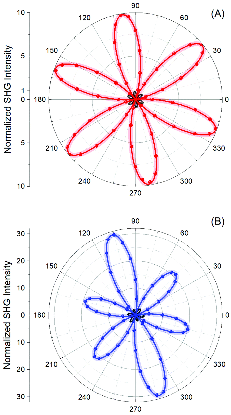 | ||
| Fig. 4 Experimental SHG intensity as a function of pump polarization angle in the perpendicular polarization configuration for (A) MoS2/FTO (red) and MoS2/glass (black); and for (B) WS2/FTO (blue) and WS2/glass (black). | ||
The same measurements were performed for WS2 deposited on FTO and glass, shown as the blue and black plots in Fig. 4B, respectively. The results indicate an SHG enhancement of 8.2 ± 2.8 times comparing FTO and glass as substrates. In the case of WS2, strain is believed to have yielded the amplitude asymmetry observed in the polarization-resolved SHG intensity plots.59–61 The origin of strain is usually attributed to the inherent lack of stiffness of PDMS used on sample preparation. PDMS being soft can get slightly deformed during transfer by the pressure exerted upon contact with the target substrate, likely being the deformation source to induce strain in the flake being transferred.60,62 In principle, and as already observed by others,63–66 the photoluminescence (PL) peak shift can be considered an indicator of how the electronic band structure is altered by the application of strain in TMDCs. In our case, we observed a shift of 0.1 eV on the WS2 PL peak comparing the flakes before and after the transfer process (see the ESI†), compatible with a strain of less than 1% in monolayer WS2.63
Nevertheless, it is possible to observe the same enhancement values, within the errors, for monolayer MoS2 and WS2 on FTO, as indeed expected and confirming that the enhancement mechanism is only dependent on the ENZ substrate, which provides a simple and easily scalable alternative for nonlinear optical wavelength conversion.
Conclusions
We reported on SHG in mechanically exfoliated monolayer TMDCs enhanced by using an epsilon-near-zero (ENZ) substrate. This substrate presents itself as an extremely simple and low-cost alternative to enhance the pump electric field at 2D materials, thus increasing the frequency converted intensity. By optimizing the substrate thickness and operating with a pump near the ENZ point, it is possible to enhance the nonlinear optical fields, with increased potential for practical nonlinear applications. The converted signal was experimentally found to be 7.2 ± 2.1 and 8.2 ± 2.8 times higher on the ENZ substrate than on glass, for MoS2 and WS2, respectively, agreeing with theoretical predictions.Methods
Theoretical model
An extended description of the theoretical model can be found in the ESI.† Briefly, the sample is modeled as a multilayer system with the z-direction normal to the surface. Layer 1 is a semi-infinite vacuum region (z > 0), where the pump source is located. Layer 2 corresponds to the FTO substrate of thickness d(0 > z >−d), with a monolayer MoS2 sheet on top (at z = 0); and layer 3 is a semi-infinite glass slide with z <−d, where the detector is placed. To evaluate the SHG fields in layer 3, the pump fields are first calculated. Then, the SHG fields above and below the MoS2 are calculated and subsequently propagated through the different layers. In this way, the transmitted SHG field in layer 3 was obtained. Green's function formalism, with the infinitesimal vacuum gap approach, is used to obtain the SHG fields radiated by the monolayer MoS2 on FTO and on glass. To compare the field intensity on both substrates, the MoS2/FTO SHG intensity was normalized by the MoS2/glass SHG intensity (see the ESI† for detailed models). The dielectric function of FTO was described by using the Drude free electron model, where ε∞ = 2.95, εp = 1.89 × 10¹⁵ s−1 and γ = 0.9 × 10¹⁴ s−1, which were obtained by fitting experimental transmission curves (see the ESI†). The glass refractive index was taken to be given by57
Sample preparation and characterization
MoS2 and WS2 monolayer flakes were mechanically exfoliated onto UV-ozone treated polydimethylsiloxane (PDMS) and transferred to the surfaces of FTO and glass (for comparison). The sputter coated FTO substrate was kindly provided by MSE Supplies LLC (TEC™ 7, 7–8 ohm sq.−1, on a 2.2 mm thick soda lime glass) with a root mean square (RMS) roughness of approximately 17.8 nm, as determined by atomic force microscopy (AFM). The substrate was polished, which reduced the intrinsic roughness to 1.7 nm, allowing for a better adhesion of the monolayer flakes during the transfer process (see Fig. S4 in the ESI†). Substrate thickness before and after polishing was determined by interferometric measurements (3D laser scanning microscope – model VK-X200 at 408 nm), yielding 610 nm and 520 nm, respectively.Flake characterization was performed by Raman spectroscopy (WITec Alpha 300R) for both MoS2 and WS2 with 532 nm excitation (see Fig. S5 and S6 in the ESI†). After the flakes were transferred to the substrates (FTO and glass), samples were annealed in a vacuum at 200 °C for 2 h followed by additional vacuum annealing for 3 h at 200 °C to minimize polymer residue and strain.60 To minimize possible substrate thickness/roughness variations, MoS2 and WS2 flakes were transferred to the same FTO substrate. The glass sample was the same as the one used for FTO deposition.
Conflicts of interest
There are no conflicts to declare.Acknowledgements
This work was funded by FAPESP (Thematic Projects 2015/11779-4 and 2018/25339-4), the Brazilian Nanocarbon Institute of Science and Technology (INCT/Nanocarbon – 88887.195743/2018-00), CNPq, FAPEMIG and CAPES-PRINT (Grant 88887.310281/2018-00). P. G. V. was supported by CAPES scholarships (grant no. 88887.195743/2018-00 and 88887.370132/2019-00). The FTO substrates were kindly provided by MSE Supplies LLC (https://www.msesupplies.com). The use of the 3D laser scanning microscope – model VK-X200 at LNNano facilities for FTO thickness measurement (process: DSF-LD-25815) is gratefully acknowledged.Notes and references
- B. Guo, Q. Lan Xiao, S. Hao Wang and H. Zhang, Laser Photonics Rev., 2019, 13, 1–46 Search PubMed.
- J. W. You, S. R. Bongu, Q. Bao and N. C. Panoiu, Nanophotonics, 2018, 8, 63–97 Search PubMed.
- C. B. De Araújo, A. S. L. Gomes and G. Boudebs, Rep. Prog. Phys., 2016, 79, 036401 CrossRef.
- A. Autere, H. Jussila, Y. Dai, Y. Wang, H. Lipsanen and Z. Sun, Adv. Mater., 2018, 30, 1705963 CrossRef.
- R. Wang, H. Chien, J. Kumar, N. Kumar, H. Chiu and H. Zhao, ACS Appl. Mater. Interfaces, 2014, 6, 314–318 CrossRef CAS.
- X. Zhou, J. Cheng, Y. Zhou, T. Cao, H. Hong, Z. Liao, S. Wu, H. Peng, K. Liu and D. Yu, J. Am. Chem. Soc., 2015, 137, 7994–7997 CrossRef CAS.
- N. Kumar, S. Najmaei, Q. Cui, F. Ceballos, P. M. Ajayan, J. Lou and H. Zhao, Phys. Rev. B: Condens. Matter Mater. Phys., 2013, 87, 1–6 Search PubMed.
- Y. Li, Y. Rao, K. F. Mak, Y. You, S. Wang, C. R. Dean and T. F. Heinz, Nano Lett., 2013, 13, 3329–3333 CrossRef CAS.
- A. Autere, H. Jussila, A. Marini, J. R. M. M. Saavedra, Y. Dai, A. Säynätjoki, L. Karvonen, H. Yang, B. Amirsolaimani, R. A. Norwood, N. Peyghambarian, H. Lipsanen, K. Kieu, F. J. G. De Abajo and Z. Sun, Phys. Rev. B, 2018, 98, 21–23 CrossRef.
- L. M. Malard, T. V. Alencar, A. P. M. Barboza, K. F. Mak and A. M. De Paula, Phys. Rev. B: Condens. Matter Mater. Phys., 2013, 87, 1–5 CrossRef.
- M. J. L. F. Rodrigues, C. J. S. de Matos, Y. W. Ho, H. Peixoto, R. E. P. de Oliveira, H. Y. Wu, A. H. C. Neto and J. Viana-Gomes, Adv. Mater., 2016, 28, 10693–10700 CrossRef CAS.
- R. I. Woodward, R. T. Murray, C. F. Phelan, R. E. P. de Oliveira, T. H. Runcorn, E. J. R. Kelleher, S. Li, E. C. de Oliveira, G. J. M. Fechine, G. Eda and C. J. S. de Matos, 2D Mater., 2016, 4, 011006 CrossRef.
- D. Li, W. Xiong, L. Jiang, Z. Xiao, H. Rabiee Golgir, M. Wang, X. Huang, Y. Zhou, Z. Lin, J. Song, S. Ducharme, L. Jiang, J. F. Silvain and Y. Lu, ACS Nano, 2016, 10, 3766–3775 CrossRef CAS.
- T. Jakubczyk, V. Delmonte, M. Koperski, K. Nogajewski, C. Faugeras, W. Langbein, M. Potemski and J. Kasprzak, Nano Lett., 2016, 16, 5333–5339 CrossRef CAS.
- R. Ciesielski, A. Comin, M. Handloser, K. Donkers, G. Piredda, A. Lombardo, A. C. Ferrari and A. Hartschuh, Nano Lett., 2015, 15, 4968–4972 CrossRef CAS.
- H. Liu, Y. Li, Y. S. You, S. Ghimire, T. F. Heinz and D. A. Reis, Nat. Phys., 2017, 13, 262–265 Search PubMed.
- M. S. Mrudul, N. Tancogne-Dejean, A. Rubio and G. Dixit, npj Comput. Mater., 2020, 6, 1–9 Search PubMed.
- N. Tancogne-dejean and A. Rubio, Sci. Adv., 2018, 4, 1–6 Search PubMed.
- C. Janisch, N. Mehta, D. Ma, A. L. Elías, N. Perea-López, M. Terrones and Z. Liu, Opt. Lett., 2014, 39, 383 CrossRef CAS.
- R. J. Shiue, D. K. Efetov, G. Grosso, C. Peng, K. C. Fong and D. Englund, Nanophotonics, 2017, 6, 1329–1342 CAS.
- X. Liu and M. C. Hersam, Nat. Rev. Mater., 2019, 4, 669–684 CrossRef.
- Y. Q. An, J. E. Rowe, D. B. Dougherty, J. U. Lee and A. C. Diebold, Phys. Rev. B: Condens. Matter Mater. Phys., 2014, 89, 1–13 Search PubMed.
- H. Yu, D. Talukdar, W. Xu, J. B. Khurgin and Q. Xiong, Nano Lett., 2015, 15, 5653–5657 CrossRef CAS.
- H. Hu, K. Wang, H. Long, W. Liu, B. Wang and P. Lu, Nano Lett., 2015, 15, 3351–3357 CrossRef CAS.
- G. Wang, X. Marie, I. Gerber, T. Amand, D. Lagarde, L. Bouet, M. Vidal, A. Balocchi and B. Urbaszek, Phys. Rev. Lett., 2015, 114, 1–6 Search PubMed.
- N. K. Balla, M. O'Brien, N. McEvoy, G. S. Duesberg, H. Rigneault, S. Brasselet and D. McCloskey, ACS Photonics, 2018, 5, 1235–1240 CrossRef CAS.
- M. L. Trolle, Y. C. Tsao, K. Pedersen and T. G. Pedersen, Phys. Rev. B: Condens. Matter Mater. Phys., 2015, 92, 1–5 Search PubMed.
- K. Q. Lin, S. Bange and J. M. Lupton, Nat. Phys., 2019, 15, 242–246 Search PubMed.
- A. R. Khan, B. Liu, L. Zhang, Y. Zhu, X. He, L. Zhang, T. Lü and Y. Lu, Adv. Opt. Mater., 2020, 2000441, 1–7 Search PubMed.
- K. L. Seyler, J. R. Schaibley, P. Gong, P. Rivera, A. M. Jones, S. Wu, J. Yan, D. G. Mandrus, W. Yao and X. Xu, Nat. Nanotechnol., 2015, 10, 407–411 CrossRef CAS.
- B. Metzger, L. Gui, J. Fuchs, D. Floess, M. Hentschel and H. Giessen, Nano Lett., 2015, 15, 3917–3922 CrossRef CAS.
- W. P. Guo, W. Y. Liang, C. W. Cheng, W. L. Wu, Y. T. Wang, Q. Sun, S. Zu, H. Misawa, P. J. Cheng, S. W. Chang, H. Ahn, M. T. Lin and S. Gwo, Nano Lett., 2020, 20, 2857–2864 CrossRef CAS.
- X. Han, K. Wang, P. D. Persaud, X. Xing, W. Liu, H. Long, F. Li, B. Wang, M. R. Singh and P. Lu, ACS Photonics, 2020, 7, 562–568 CrossRef CAS.
- X. Wen, G. Li, C. Gu, J. Zhao, S. Wang, C. Jiang, S. Palomba, C. Martijn De Sterke and Q. Xiong, ACS Photonics, 2018, 5, 2087–2093 CrossRef CAS.
- R. Czaplicki, A. Kiviniemi, M. J. Huttunen, X. Zang, T. Stolt, I. Vartiainen, J. Butet, M. Kuittinen, O. J. F. Martin and M. Kauranen, Nano Lett., 2018, 18, 7709–7714 CrossRef CAS.
- X. Li, W. Liu, Y. Song, C. Zhang, H. Long, K. Wang, B. Wang and P. Lu, Adv. Opt. Mater., 2019, 7, 2–7 Search PubMed.
- D. Li, C. Wei, J. Song, X. Huang, F. Wang, K. Liu, W. Xiong, X. Hong, B. Cui, A. Feng, L. Jiang and Y. Lu, Nano Lett., 2019, 19, 4195–4204 CrossRef CAS.
- K. Koshelev, Y. Tang, K. Li, D. Y. Choi, G. Li and Y. Kivshar, ACS Photonics, 2019, 6, 1639–1644 CrossRef CAS.
- N. Yu and F. Capasso, Nat. Mater., 2014, 13, 139–150 CrossRef CAS.
- K. Koshelev, A. Bogdanov and Y. Kivshar, Sci. Bull., 2019, 64, 836–842 CrossRef.
- K. Koshelev, S. Lepeshov, M. Liu, A. Bogdanov and Y. Kivshar, Phys. Rev. Lett., 2018, 121, 193903 CrossRef.
- Q. Yuan, L. Fang, H. Fang, J. Li, T. Wang, W. Jie, J. Zhao and X. Gan, ACS Photonics, 2019, 6, 2252–2259 CrossRef CAS.
- X. T. Gan, C. Y. Zhao, S. Q. Hu, T. Wang, Y. Song, J. Li, Q. H. Zhao, W. Q. Jie and J. L. Zhao, Light: Sci. Appl., 2018, 7, 17126 CrossRef CAS.
- L. Fang, Q. Yuan, H. Fang, X. Gan, J. Li, T. Wang, Q. Zhao, W. Jie and J. Zhao, Adv. Opt. Mater., 2018, 6, 1800698 CrossRef.
- J. K. Day, M.-H. Chung, Y.-H. Lee and V. M. Menon, Opt. Mater. Express, 2016, 6, 2360 CrossRef CAS.
- T. K. Fryett, K. L. Seyler, J. Zheng, C. H. Liu, X. Xu and A. Majumdar, 2D Mater., 2017, 4, 015031 CrossRef.
- H. Chen, V. Corboliou, A. S. Solntsev, D. Choi, M. A. Vincenti, D. De Ceglia, C. De Angelis, Y. Lu and D. N. Neshev, Light: Sci. Appl., 2017, 6, e17060 CrossRef CAS.
- R. Czaplicki, M. Zdanowicz, K. Koskinen, H. Husu, J. Laukkanen, M. Kuittinen and M. Kauranen, Opt. Express, 2011, 19, 541–542 CrossRef.
- Y. R. Shen, Annu. Rev. Phys. Chem., 1989, 40, 327–350 CrossRef CAS.
- I. Liberal and N. Engheta, Nat. Photonics, 2017, 11, 149–158 CrossRef CAS.
- R. Maas, J. Parsons, N. Engheta and A. Polman, Nat. Photonics, 2013, 7, 907–912 CrossRef CAS.
- J. R. Hendrickson, S. Vangala, C. Dass, R. Gibson, J. Goldsmith, K. Leedy, D. E. Walker, J. W. Cleary, W. Kim and J. Guo, ACS Photonics, 2018, 5, 776–781 CrossRef CAS.
- E. Feigenbaum, K. Diest and H. A. Atwater, Nano Lett., 2010, 10, 2111–2116 CrossRef CAS.
- J. E. Sipe, J. Opt. Soc. Am. B, 1987, 4, 481 CrossRef.
- J. E. Sipe and D. J. Moss, Phys. Rev. B: Condens. Matter Mater. Phys., 1987, 35, 1129–1141 CrossRef.
- J. J. Dean and H. M. Van Driel, Phys. Rev. B: Condens. Matter Mater. Phys., 2010, 82, 1–10 Search PubMed.
- M. Rubin, Sol. Energy Mater., 1985, 12, 275–288 CrossRef CAS.
- Z. Wang, C. Chen, K. Wu, H. Chong and H. Ye, Phys. Status Solidi A, 2019, 216, 1–12 CrossRef.
- L. Mennel, M. Paur and T. Mueller, APL Photonics, 2019, 4, 034404 CrossRef CAS.
- A. Jain, P. Bharadwaj, S. Heeg, M. Parzefall, T. Taniguchi, K. Watanabe and L. Novotny, Nanotechnology, 2018, 29, 265203 CrossRef.
- J. Liang, J. Zhang, Z. Li, H. Hong, J. Wang, Z. Zhang, X. Zhou, R. Qiao, J. Xu, P. Gao, Z. Liu, Z. Liu, Z. Sun, S. Meng, K. Liu and D. Yu, Nano Lett., 2017, 17, 7539–7543 CrossRef CAS.
- A. Castellanos-Gomez, M. Buscema, R. Molenaar, V. Singh, L. Janssen, H. S. J. van der Zant and G. A. Steele, 2D Mater., 2014, 1, 011002 CrossRef.
- S. Pak, J. Lee, Y. W. Lee, A. R. Jang, S. Ahn, K. Y. Ma, Y. Cho, J. Hong, S. Lee, H. Y. Jeong, H. Im, H. S. Shin, S. M. Morris, S. Cha, J. I. Sohn and J. M. Kim, Nano Lett., 2017, 17, 5634–5640 CrossRef CAS.
- S. Aas and C. Bulutay, Opt. Express, 2018, 26, 28672 CrossRef CAS.
- A. V. Tyurnina, D. A. Bandurin, E. Khestanova, V. G. Kravets, M. Koperski, F. Guinea, A. N. Grigorenko, A. K. Geim and I. V. Grigorieva, ACS Photonics, 2019, 6, 516–524 CrossRef CAS.
- S. Manzeli, A. Allain, A. Ghadimi and A. Kis, Nano Lett., 2015, 15, 5330–5335 CrossRef.
Footnote |
| † Electronic supplementary information (ESI) available. See DOI: 10.1039/d0na00779j |
| This journal is © The Royal Society of Chemistry 2021 |