
 Open Access Article
 This Open Access Article is licensed under a
 Creative Commons Attribution 3.0 Unported Licence
Mixed-dimensional InAs nanowire on layered molybdenum disulfide heterostructures via selective-area van der Waals epitaxy†
Mohadeseh A.
Baboli
 ab,
Alireza
Abrand
ab,
Robert A.
Burke
cd,
Anastasiia
Fedorenko
ab,
Thomas S.
Wilhelm
ab,
Stephen J.
Polly
b,
Madan
Dubey
c,
Seth M.
Hubbard
ab and
Parsian K.
Mohseni
*ab
ab,
Alireza
Abrand
ab,
Robert A.
Burke
cd,
Anastasiia
Fedorenko
ab,
Thomas S.
Wilhelm
ab,
Stephen J.
Polly
b,
Madan
Dubey
c,
Seth M.
Hubbard
ab and
Parsian K.
Mohseni
*ab
aMicrosystems Engineering, Rochester Institute of Technology, Rochester, NY 14623, USA. E-mail: pkmohseni@rit.edu
bNanoPower Research Laboratories, Rochester Institute of Technology, Rochester, NY 14623, USA
cSensors and Electron Devices Directorate, U.S. Army Research Laboratory, Adelphi, MD 20783, USA
dGeneral Technical Services, LLC, Wall, NJ 07727, USA
First published on 19th March 2021
Abstract
Self-assembly of vertically aligned III–V semiconductor nanowires (NWs) on two-dimensional (2D) van der Waals (vdW) nanomaterials allows for integration of novel mixed-dimensional nanosystems with unique properties for optoelectronic and nanoelectronic device applications. Here, selective-area vdW epitaxy (SA-vdWE) of InAs NWs on isolated 2D molybdenum disulfide (MoS2) domains is reported for the first time. The MOCVD growth parameter space (i.e., V/III ratio, growth temperature, and total molar flow rates of metalorganic and hydride precursors) is explored to achieve pattern-free positioning of single NWs on isolated multi-layer MoS2 micro-plates with one-to-one NW-to-MoS2 domain placement. The introduction of a pre-growth poly-L-lysine surface treatment is highlighted as a necessary step for mitigation of InAs nucleation along the edges of triangular MoS2 domains and for NW growth along the interior region of 2D micro-plates. Analysis of NW crystal structures formed under the optimal SA-vdWE condition revealed a disordered combination of wurtzite and zinc-blend phases. A transformation of the NW sidewall faceting structure is observed, resulting from simultaneous radial overgrowth during axial NW synthesis. A common lattice arrangement between axially-grown InAs NW core segments and MoS2 domains is described as the epitaxial basis for vertical NW growth. A model is proposed for a common InAs/MoS2 sub-lattice structure, consisting of three multiples of the cubic InAs unit cell along the [2![[1 with combining macron]](https://www.rsc.org/images/entities/char_0031_0304.gif) ] direction, commensurately aligned with a 14-fold multiple of the Mo–Mo (or S–S) spacing along the [100] direction of MoS2 hexagonal lattice. The SA-vdWE growth mode described here enables controlled hybrid integration of mixed-dimensional III–V-on-2D heterostructures as novel nanosystems for applications in optoelectronics, nanoelectronics, and quantum enabling technologies.
] direction, commensurately aligned with a 14-fold multiple of the Mo–Mo (or S–S) spacing along the [100] direction of MoS2 hexagonal lattice. The SA-vdWE growth mode described here enables controlled hybrid integration of mixed-dimensional III–V-on-2D heterostructures as novel nanosystems for applications in optoelectronics, nanoelectronics, and quantum enabling technologies.
Introduction
The emergence of two-dimensional (2D) atomically thin materials with novel and tunable physical properties has opened new opportunities for design of next-generation nanoscale electronic devices.1 Since the isolation of single layer graphene in 2004,2 significant effort has been dedicated to the synthesis and exploration of numerous alternative 2D materials. Among several classes of layered materials such as metal chalcogenides, boron nitride, oxides and oxychlorides, only a few have been successfully isolated in the form of 2D mono- or multi-layers with high crystalline quality. Transition metal dichalcogenides (TMDCs) such as molybdenum disulfide (MoS2), molybdenum diselenide (MoSe2), and tungsten diselenide (WSe2) are among the most extensively studied van der Waals (vdW) layered compounds. Based on the number of transition metal d-electrons, the TMDCs demonstrate metallic,3,4 half-metallic magnetism,5 semiconducting,6 or superconducting characteristics.7 For example, semiconductor compounds based on Mo and W, with bandgaps ranging from the visible to the near-infrared, have been widely studied and employed in numerous emerging device applications.8–10In particular, MoS2 is one of the most studied 2D TMDC materials owing to its many outstanding properties.11 Similar to other TMDC compounds, MoS2 exhibits a layered atomic structure with weak vdW interactions between layers and strong intra-layer bonding. Each monolayer of MoS2 is a tri-layer sandwich structure, which consists of hexagonal S and Mo atomic layers wherein each Mo atom resides at the center of six S atoms creating a trigonal prism. Interestingly, in its bulk form, MoS2 displays an indirect bandgap (Eg = 1.2 eV), whereas monolayer MoS2 has a direct bandgap (Eg = 1.8 eV).12 The transition from bulk MoS2 with indirect bandgap to its monolayer form with direct bandgap was predicted theoretically by Li et al. in 2007.13 In 2010, Splendiani et al. investigated this bandgap transition by photoluminescence (PL) of ultrathin MoS2 layers and found PL enhancement by decreasing the number of layers. In particular, they observed that monolayer MoS2 shows strong emission peaks between 627 nm and 677 nm.14 With these properties, MoS2 is a great candidate for integration in devices such as field-effect transistors (FETs),15,16 light-emitting diodes (LEDs),17 photodetectors,18 and photovoltaic solar cells.19
Heterostructures and superlattices are essential building blocks of electronic and optoelectronic devices. Among the current material integration techniques, chemical epitaxy approaches such as molecular beam epitaxy (MBE) and metalorganic chemical vapor deposition (MOCVD) have offered the highest-quality implementation of more complex heterostructure designs. Chemical epitaxy of two covalently bonded material systems is based on one-to-one chemical bond formation at the heterointerface. For materials with significantly dissimilar lattice structures, misfit dislocations can form at the heterointerface and lead to the formation of extended threading dislocations. This can result in substantial degradation of the properties of the heterostructure. Thus, conventional epitaxy of high crystalline quality heterostructures is generally limited to materials with comparable lattice parameters (i.e., lattice constants, symmetry, thermal expansion coefficient, and polarity).
The class of 2D materials with inert surfaces that are free of dangling bonds provides an alternative pathway for integration of heterostructures via van der Waals epitaxy (vdWE), wherein two or more dissimilar 2D materials can be assembled together via weak interplanar vdW interactions. Unlike conventional epitaxy, covalent strain sharing is not permitted at the heterointerface during vdWE. Thus, vdW heterostructures can be formed using a wide range of 2D materials with dissimilar crystal structures. For example, high performance photodetectors based on various vdW heterostructures such as MoS2/tin diselenide (SnSe2),20 MoS2/graphene/tungsten diselenide (WSe2),21 and MoS2/black phosphorus22 have been reported. Moreover, such a hybrid integration technique is not limited to 2D layered materials, and can be applied to materials of dissimilar dimensionality to form mixed-dimensional heterostructures of radically different crystal structures. Recent research on mixed-dimensional vdW heterostructures, as well as their challenges and opportunities, have been reviewed in ref. 23 and 24.
Likewise, semiconductor nanowires (NWs) provide an excellent platform for the formation of complex 3D heterostructures, wherein dissimilar compounds can be monolithically integrated in both radial and axial directions.25 This flexibility in design of active nanostructures can provide promising solutions for design of high-performance electronic,26 optoelectronic,25,27 and photonic28 devices. In addition, owning to their large surface area-to-volume ratio and small footprint on the substrate, NWs exhibit excellent strain tolerance. Therefore, III–V NWs offer outstanding potential for integration with a variety of different foreign substrates such as silicon,29–32 germanium,33 glass,34 indium tin oxide,35 and 2D vdW surfaces like graphene.36–41
In this paper, we present lithography-free hybrid integration of mixed-dimensional heterostructures composed of InAs NWs and MoS2 micro-plates via selective-area vdWE (SA-vdWE) by MOCVD. The growth parameter space is mapped by altering the V/III ratio, growth temperature, and total flow rate of the precursors. The influence of these parameters on self-assembly of vertically-aligned InAs NWs and growth of parasitic islands on 2D MoS2 surfaces is explored. Growth trends are discussed independently for each set of growth trials. The impact of pre-growth surface treatment on MoS2 is investigated toward realization of site-controlled SA-vdWE of a single InAs NW on each isolated triangular MoS2 domain. The crystal structure of InAs NWs grown under the optimal growth conditions, which are conducive to the formation of a single NW per MoS2 micro-plate, is analyzed. Finally, the common sub-lattice registry between vertical InAs NWs and MoS2 flakes is discussed using a super-cell model based on the coincident alignment of NW sidewall facets and MoS2 micro-island domain edges. The results of this study are expected to provide a foundation for future investigations of mixed-dimensional III–V-on-2D vdW heterostructures for applications in nanoscale optoelectronic and electronic devices.
Experimental details
The MoS2 triangular domains were grown on thermally oxidized (220 nm SiO2) Si (100) substrates by atmospheric pressure powder vaporization. Prior to growth, the substrates were cleaned in a piranha solution for 15 min followed by 5 min soaks in deionized (DI) water, acetone, and isopropyl alcohol. Afterwards, 40 μL of perylene-3,4,9,10-tetracarboxylic acid tetrapotassium salt (PTAS) was spin coated on each sample as a seeding layer for growth. Next, ∼20 mg of MoO3 powder (Sigma-Aldrich, ≥99.5%) was added to an alumina boat (AdValue Technology), and PTAS-coated substrates were placed on top of the alumina boat face up with a 1.2 mm gap between neighboring samples. The boat was loaded into the center of the furnace. 15–17 mg of sulfur powder (Sigma-Aldrich, 99.8%) was loaded in another alumina boat and placed in a region outside of the furnace where the temperature could be independently controlled by a heating tape. The growth process was performed in the tube furnace at a sample temperature of 700 °C and sulfur temperature of 250 °C. The growth was carried out for 10 min, during which 5 sccm of argon (Airgas, 99.999%) was used as a carrier gas. After the growth was complete, the tube furnace was opened and the argon flow rate was increased to 200 sccm to quench the growth process. The isolated MoS2 triangular micro-plates with side lengths ranging between ∼3 μm and 5 μm act as the growth surface in all InAs crystal growth experiments. A top-view optical image of a representative MoS2 sample surface used for SA-vdWE experiments is shown in the ESI (Fig. S1).†For growth of InAs NWs, trimethyl-indium [TMIn; (CH3)3In] and arsine (AsH3) were used as precursors for the supply of group-III and group-V growth species, respectively, in an Aixtron 3 × 2′′ close-coupled showerhead MOCVD reactor. For all growth runs, substrates were heated to the targeted growth temperature under constant AsH3 flow. Growth of NWs was initiated by the introduction of TMIn flow into the chamber. After a growth duration of 300 seconds, NW growth was terminated by turning off the TMIn flow. All samples were cooled under a constant AsH3 flow.
The optimal SA-vdWE conditions were established by investigating the growth parameter space during three sets of experiments. The three sets of growth runs explored the MOCVD parameter space in the following ranges: (i) V/III ratio was varied between 5 and 250, (ii) TMIn flow rate (χTMIn) was varied between 8 and 32 μmol min−1 under constant V/III ratio, and (iii) the growth temperature (TG) was varied between 600 °C and 750 °C, as monitored by susceptor thermocouple setpoint. Based on LayTec EpiTT emissivity-corrected pyrometry measurements, the true temperature at the MoS2 surface is ∼120 °C lower than the setpoint temperature. Therefore, thermal decomposition of MoS2 domains is not expected under these growth conditions.42 For all trials, hydrogen (H2) was used as the carrier gas with a total flow rate of 14 L min−1, and the reactor pressure was kept constant at 100 mbar. During the initial series of parameter space optimization experiments, no surface treatment was performed on MoS2 surfaces prior to loading in the MOCVD reactor. Next, a surface treatment step was performed prior to loading to achieve selective-area single NW synthesis per MoS2 domain. This involved dipping MoS2 samples in a poly-L-lysine [PLL; (C6H12N2O)n] solution for a duration of 120 seconds, followed by rinsing in deionized water for 5 seconds.
The morphology of as-grown samples was imaged using a Hitachi S-4000 SEM. The surface roughness of pre-treated and PLL-treated MoS2 nano-sheets was measured using a Bruker DI-3000 atomic force microscope (AFM). The crystal structure of NWs was characterized using a FEI F20 high-resolution transmission electron microscope (HR-TEM). TEM lamellae were prepared using a FEI Strata 400 STEM focused ion beam (FIB). Selected-area electron diffraction (SAED) patterns were obtained using the same instrument. Compositional analysis at the InAs/MoS2 interface was performed through electron energy loss spectroscopy (EELS) using a Nion UltraSTEM 100 TEM.
Results and discussions
The main objective of this study is to investigate epitaxy of a covalently bonded III–V compound system upon a 2D vdW layered TMDC film. Here, CVD-grown discrete MoS2 micro-plates are used as the growth surface for pseudo-vdWE of InAs NWs. In the first part of this study, the MOCVD growth parameter space is mapped (i.e., V/III ratio, TG, and χTMIn) to find suitable conditions for vdWE of vertical InAs NWs on MoS2 micro-plates. To investigate the influence of each parameter independently, one parameter is varied in each set of growth trials while the other two parameters are kept constant. Similar to previously reported studies on integration of III–V NWs with vdW-surfaces, polycrystalline parasitic islands are formed on the growth surface along with vertically-oriented NWs.38–41 To evaluate each trial run, tilted-view SEM images of 20 MoS2 micro-plates are used to measure the mean NW length and diameter values. In the second part of this study, the objective is to eliminate the formation of parasitic islands and to control crystal growth such that a single NW is formed on each isolated MoS2 domain. This is achieved by focusing on the surface and plate-edge characteristics of MoS2 micro-plates as well as further tuning of growth conditions.In the first set of experiments, the influence of V/III ratio on the growth of InAs NWs on 2D MoS2 micro-plates is investigated. Here, the V/III ratio (i.e., defined by molar flow ratio) is changed over the range of 5 to 250 at a growth temperature of 650 °C. The V/III is modified by altering the molar flow rate of AsH3 under a constant molar flow rate of TMIn (i.e., χTMIn = 16 μmol min−1). Shown in Fig. 1(a)–(d) are 45° tilted-view SEM images of as-grown samples. At V/III = 5 [Fig. 1(a)], the MoS2 micro-plates are fully covered with polycrystalline InAs islands. Increasing the V/III ratio to a range of 25 to 125 results in the formation of NWs along the central region of each MoS2 domain, as well as parasitic islands around the plate-edges. At a V/III ratio of 250, InAs crystal formation is strictly limited to the edges of MoS2 domains, and no growth takes place along the interior area of the micro-plates.
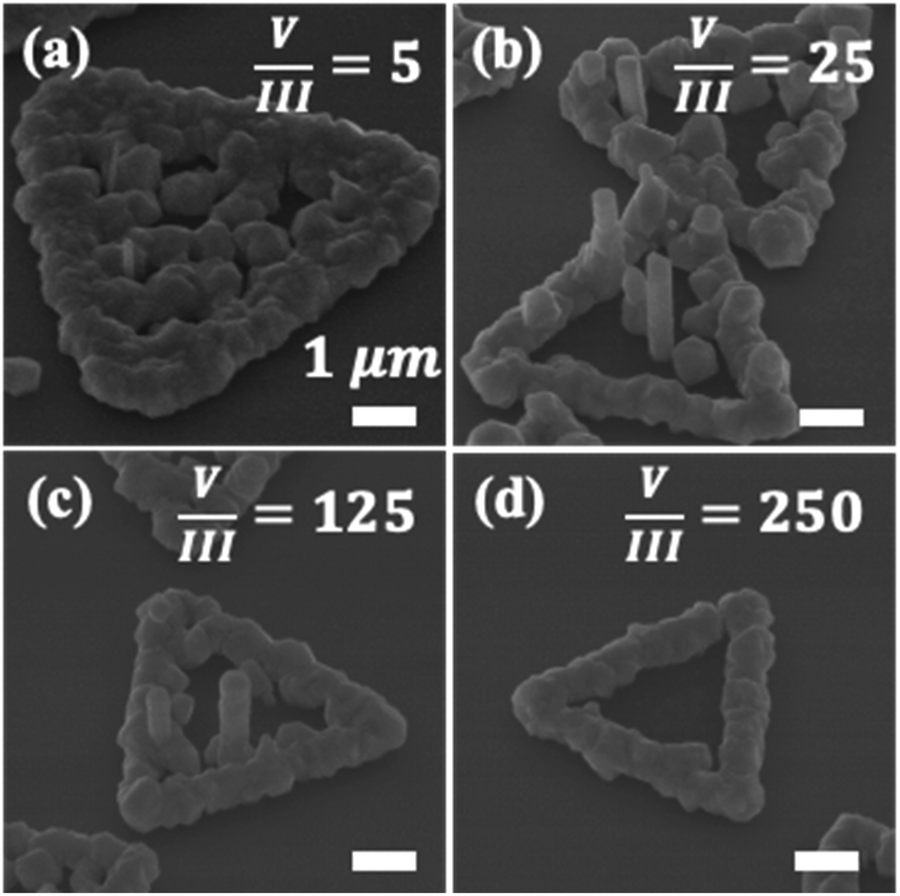 | ||
| Fig. 1 Influence of V/III ratio on the growth of InAs NWs on MoS2 micro-plates. 45° tilted-view SEM images of as-grown samples at V/III ratios of (a) 5, (b) 25, (c) 125, and (d) 250, with χTMIn = 16 μmol min−1 and TG = 650 °C. All scale bars represent 1 μm. | ||
To understand these results, it should be noted that the sticking coefficient of MoS2 micro-plates is not homogenous throughout each domain. When adatoms impinge upon a surface, there are three possibilities: (i) to adsorb on an impingement site, (ii) to migrate on the surface and adsorb on a secondary surface site, or (c) to desorb from the surface. The sticking coefficient is defined as the ratio of the number of adsorbed atoms to the number of atoms that either migrate or desorb.43 Here, for instance, the SiOx surface that is exposed between neighboring MoS2 domains has a very low sticking coefficient, and no crystal growth is observed on the oxide surface. On the MoS2 micro-plates, however, the potential for adatom nucleation is greater at the domain edge sites compared to the interior domain surface due to an abundance of available dangling bonds at the plate-edges. Consequently, the domain edges serve as nucleation sites for InAs island growth under all V/III ratios employed in this study. However, the V/III ratio serves to further tune the surface migration of adatoms. Under low V/III ratio growth conditions (i.e., V/III = 5), the growth species can reach the central region of the MoS2 microplates, likely due to their enhanced surface migration. A similar effective enhancement of adatom migration under low V/III growth conditions was also observed during InAs NW vdWE on graphene.38 In contrast, under high V/III ratio growth conditions (i.e., V/III = 250), crystal growth is limited to parasitic island formation around the edges of MoS2 domains, likely due to an effective reduction in adatom surface migration coupled with the availability of bonding sites at the domain edges. At the intermediate V/III ratio range (i.e., V/III = 25 to 125), the growth species that are able to reach the interior segment of the MoS2 micro-plates can contribute to the formation of vertical NWs. Therefore, intermediate V/III ratio values represent favorable growth condition for self-assembly of vertical InAs NWs on MoS2 domains under the pseudo-vdWE regime. The difference in dimensions of NWs grown under V/III ratios of 25 and 125 is negligible. At V/III = 25, the mean NW length is 1.92 μm and the mean NW diameter is 0.40 μm, whereas at V/III = 125, mean NW length and diameter values of 1.78 μm and 0.44 μm are measured, respectively.
Next, the influence of growth rate was investigated by altering the total molar flow rate of both metalorganic and hydride precursors (i.e., χTotal = χAsH3 + χTMIn) under a constant V/III ratio of 25 and growth temperature of 650 °C. To avoid confusion, the results are discussed with references to the molar flow rate of TMIn only (i.e., χTMIn). Fig. 2(a)–(d) shows as-grown InAs/MoS2 samples formed at various χTMIn values in the range of 8 to 32 μmol min−1. At χTMIn = 8 μmol min−1, growth is limited to the edges of MoS2 micro-plates. This results in the formation of NWs as well as parasitic islands, while no growth is observed along the interior region of the MoS2 domains. By increasing the total flow rate of the precursors, the growth front is no longer localized to the MoS2 plate-edges, and nucleation proceeds toward the center of each domain. Under the intermediate total flow rate range (i.e., χTMIn = 16 μmol min−1 to 24 μmol min−1), growth of NWs is predominantly limited to the central region of each MoS2 micro-plate, while parasitic islands are observed along the plate-edges. In the case of χTMIn = 32 μmol min−1, the MoS2 surface is fully coated with a continuous polycrystalline film of InAs, likely formed due to lateral coalescence of parasitic islands.
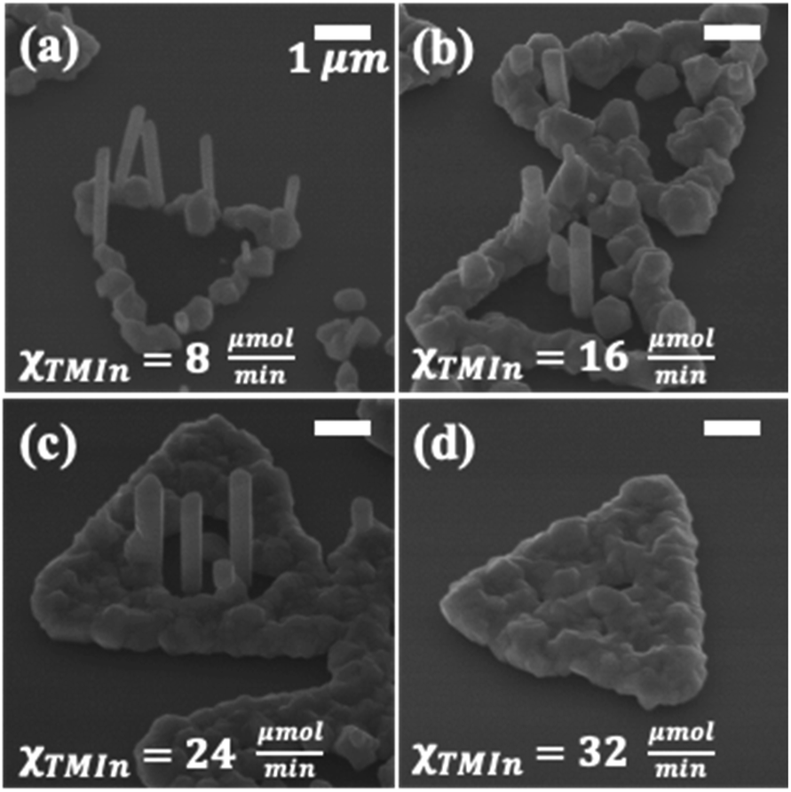 | ||
| Fig. 2 Influence of total precursor flow rate on growth of InAs NWs on MoS2 micro-plates. 45° tilted-view SEM images of as-grown samples at χTMIn of (a) 8 μmol min−1, (b) 16 μmol min−1, (c) 24 μmol min−1, and (d) 32 μmol min−1, with V/III = 25 and TG = 650 °C. All scale bars represent 1 μm. | ||
In the specific case of χTMIn = 8 μmol min−1, NWs with mean length and diameter values of ∼2.30 μm and ∼0.26 μm, respectively, are formed around the edge of MoS2 micro-plates. Increasing the flow rates to χTMIn = 16 μmol min−1 leads to growth of NWs with mean length of ∼1.92 μm and mean diameter of ∼0.40 μm. As the coverage of parasitic islands on MoS2 micro-plates increases under high-flow condition of χTMIn = 24 μmol min−1, the mean length of NWs reduces to ∼1.64 μm and the mean diameter of NWs increases to ∼0.54 μm. The results that involve varying the total flow rate suggest that by increasing the precursor supply, the growth front moves from the edge of MoS2 micro-plates toward the central region (i.e., within ∼2 μm from domain edges). Meanwhile, the aspect ratio of the NWs is reduced due to the role of parasitic islands as the predominant atomic sink.
Next, the influence of growth temperature on the formation of InAs NWs on MoS2 micro-plates under the pseudo-vdWE regime is investigated. Here, TG values of 600 °C, 650 °C, and 700 °C are tested under a constant V/III ratio of 25 and χTMIn = 16 μmol min−1. The corresponding growth results are shown in Fig. 3(a)–(c). At TG = 600 °C [Fig. 3(a)], the formation of NWs is fully quenched. At elevated growth temperatures of 650 °C and TG = 700 °C, however, vertical InAs NWs are self-assembled on MoS2 micro-plates, along with parasitic island formation along both central regions and edges of the MoS2 domains. For the case of TG = 650 °C, the mean NW height and diameter are measured to be 2 μm and 0.35 μm, respectively. By increasing the growth temperature to TG = 700 °C, the mean NW length and diameter are increased to 2.35 μm and 0.43 μm, respectively.
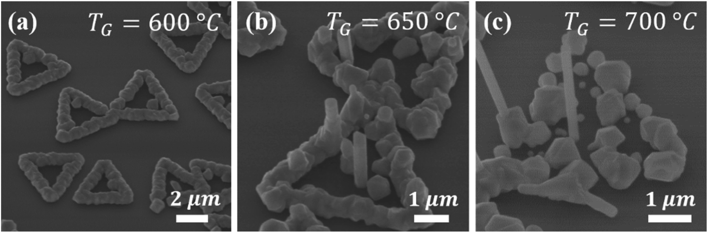 | ||
| Fig. 3 Influence of growth temperature on the synthesis of InAs NWs on MoS2 micro-plates. 45° tilted-view SEM images of as-grown samples at TG of (a) 600 °C, (b) 650 °C, and (c) 700 °C, with V/III = 25 and χTMIn = 16 μmol min−1. | ||
In the low temperature range (i.e., TG = 650 °C and below), parasitic islands are mainly formed around the edges of MoS2 micro-plates and few InAs islands are seen extending toward the interior region. This observation can be understood in terms of temperature-dependent surface mobility of the group-III species and the abundance of dangling bonds at the edges of MoS2 domains. The edges of MoS2 micro-plates act as favorable nucleation sites for growth species with low surface mobility, where adjacent parasitic islands merge and form a ring-shaped contiguous film. By increasing TG, and as a result of enhancement in the surface mobility of adatoms, the growth species can migrate toward the interior region of each MoS2 domain. It is noted that the density of parasitic islands changes dramatically by further increasing TG to 700 °C. This can be attributed to preferential incorporation of diffusive growth species into NW structures instead of parasitic islands.
Growth conditions consisting of V/III = 25, χTMIn = 16 μmol min−1, and TG = 650 °C permit vdWE of NWs along the interior surface of MoS2 domains and simultaneously result in the growth of parasitic islands around the edges of MoS2 micro-plates. On the other hand, keeping the V/III ratio and TG constant while reducing χTMIn to 8 μmol min−1 results in further reduction in the formation of parasitic islands. Moreover, the results of the TG-dependent growth trials suggest that elevated temperatures are conducive to the formation of NWs and minimum coverage of parasitic islands at the edges of MoS2 domains, which is a necessary criterion for the realization of a single NW per MoS2 micro-plate. Thus, growth parameters of V/III = 25, χTMIn = 8 μmol min−1, and TG = 750 °C are selected as the optimal SA-vdWE condition for InAs NWs on MoS2 micro-plates.
Next, the influence of a pre-growth PPL surface treatment is investigated. The effect of PLL as a coating reagent for modulating surface charge was reported by Umehara et al.44 In the current study, PLL is used for charge compensation of dangling bonds at the edges of MoS2 micro-plates. Accordingly, the diffusion barrier at the MoS2 plate-edges is expected to be affected by passivating the available dangling bonds at those regions. Furthermore, the surface roughness of individual micro-plates is investigated via AFM measurements of pre- and post-PLL treated MoS2 samples. Fig. 4 shows the height profile of a MoS2 micro-plate before and after the PLL treatment, where a pre-PLL treatment height profile is shown in black and a post-PLL treatment height profile is plotted as a blue line. This comparison indicates that the PLL surface treatment reduces the step height at the MoS2 plate-edge from ∼90 Å (pre-PLL treatment) to ∼25 Å (post-PLL treatment). This height difference may be attributed to dissolution of MoO3 during the surface treatment (i.e., due to PLL treatment and DI water rinse). Representative AFM images of the pre- and post-PLL treatment samples are shown as insets in Fig. 4, highlighted with black and blue borders, respectively. The particles seen on the surface and edges of MoS2 micro-plates are significantly reduced after the PLL-treatment. The presence of these particles are reported in various studies and is likely to be unreacted MoO3.16,42
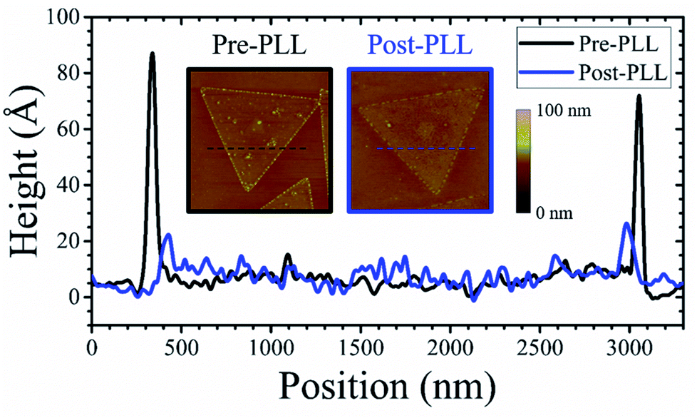 | ||
| Fig. 4 Comparison of AFM height profile of pre- and post-PLL treatment of MoS2 micro-plates surfaces. Dashed lines in the AFM image insets indicate the location of height profile measurement. | ||
The results of optimizing the growth parameter space and the influence of the PLL surface treatment are used for integration of a single InAs NW on individual, isolated, triangular MoS2 domains. To this end, samples with and without the PLL treatment are loaded for growth under the previously determined optimal SA-vdWE conditions (i.e., V/III = 25, χTMIn = 8 μmol min−1, and TG = 750 °C). Tilted-view SEM images of as-grown samples on MoS2 micro-plates without and with the PLL treatment are shown in Fig. 5(a) and (b), respectively. As expected, the use of untreated MoS2 as the growth surface under the stated MOCVD conditions results in the formation of NWs as well as parasitic islands [Fig. 5(a)]. Since this growth is performed at an elevated temperature, high surface mobility of the group-III species as well as high desorption of the group-V species lead to the formation of discrete parasitic islands, unlike the continuous polycrystalline InAs films formed at lower growth temperatures. However, the same growth conditions, when applied to a PPL treated MoS2 sample, enable pristine SA-vdWE of InAs NWs on MoS2, such that only one NW grows on each triangular MoS2 domain [Fig. 5(b)]. Importantly, parasitic crystallite growth is also eliminated along MoS2 plate-edges and surfaces. This approach allows for site-selective self-assembly of free-standing NWs near the central region of each MoS2 micro-plate. As noted earlier, PLL likely changes the MoS2 surface in two ways: (i) it allows charge compensation of dangling bonds available at the edges of MoS2 micro-plates, thereby accommodating an edge-passivation effect and quenching nucleation sites for the formation of parasitic islands; and (ii) it allows for the dissolution of the residual particles and consequently smoothens the MoS2 surface, which minimizes the availability of atomic sinks for the nucleation and formation of more than one NW or parasitic islands per MoS2 micro-plate. Table 1 summarizes the growth conditions explored in this work and the corresponding influence on the synthesis of InAs NWs on MoS2 micro-plates.
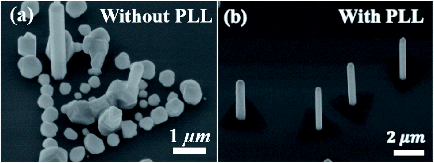 | ||
| Fig. 5 45° tilted-view SEM images of as-grown InAs NWs formed under optimal SA-vdWE growth conditions on MoS2 domains (a) without, and (b) with PLL treatment. | ||
| χ TMIn (μmol min−1) | χ AsH3 (μmol min−1) | V/III | T G (°C) | PLL | Resulting structures | |
|---|---|---|---|---|---|---|
| V/III ratio modulation | 16 | 80 | 5 | 650 | No | High domain coverage by island growth only |
| 16 | 400 | 25 | 650 | No | Predominant island growth at edges, NW growth toward central regions | |
| 16 | 2000 | 125 | 650 | No | Predominant island growth at edges, NW growth toward central regions | |
| 16 | 4000 | 250 | 650 | No | Island growth along domain edges only | |
| χ Total modulation | 8 | 200 | 25 | 650 | No | Island and NW growth along domain edges only |
| 16 | 400 | 25 | 650 | No | Predominant island growth at edges, NW growth toward central regions | |
| 24 | 600 | 25 | 650 | No | Predominant island growth at edges, NW growth toward central regions | |
| 32 | 800 | 25 | 650 | No | Nearly complete domain coverage by island growth only | |
| T G modulation | 16 | 400 | 25 | 600 | No | Island growth along domain edges only |
| 16 | 400 | 25 | 650 | No | Predominant island growth at edges, NW growth toward central regions | |
| 16 | 400 | 25 | 700 | No | Partial island growth at edges, NW growth at edges and central regions | |
| Pre-growth treatment | 8 | 200 | 25 | 750 | No | Partial island growth at edges, NW growth at edges and central regions |
| 8 | 200 | 25 | 750 | Yes | Single InAs NW growth near center of each MoS2 domain only |
To investigate the crystal structure of the NWs and to probe the InAs/MoS2 interface, TEM lamellae are prepared with a FIB from samples that were grown under the optimized SA-vdWE condition after PLL-treatment. Fig. 6 shows HR-TEM images of a NW acquired along the 〈01〉ZB zone axis of the cubic phase. The base of the NW is shown in Fig. 6(a), and the NW growth direction along 〈〉ZB is indicated with a black arrow in Fig. 6(b). The approximate locations of the HR-TEM images shown in Fig. 6(b) and (c) is illustrated in Fig. 6(a) using solid white and gray borders, respectively. Firstly, it is noted that under the SA-vdWE conditions (i.e., V/III = 25, χTMIn = 8 μmol min−1 and TG = 750 °C), the crystal structure throughout the entire length of the NW consists of a combination of zinc-blend (ZB) and wurtzite (WZ) phases. Such a characteristic disordered crystal structure with a high density of stacking faults and rotational twin planes45 was also observed for InAs NWs grown on graphene under the vdWE mode,37,41 as well as for InAs NWs grown via the SAE mode on Si substrates.46–48 The SAED pattern, shown as an inset in Fig. 6(b), exhibits streaking along the 〈〉ZB axis, which confirms the disordered crystal phase of the InAs NW. Next, the interface of the InAs NW and MoS2 micro-plate is shown in a high-magnification micrograph [Fig. 6(c)]. Here, at the location of the NW growth, a total of five vdW-bonded MoS2 layers are observed in the micro-plate. Despite the large NW diameter (i.e., >350 nm), misfit dislocations are not found at the InAs/MoS2 interface, and the NW crystal is free of threading dislocations. This is likely due to the absence of strain sharing between the dissimilar lattices. In Fig. 6(c), an abrupt heterointerface is observed that is absent of compositional grading or transitional phases. The average interplanar separation in the axial direction is measured to be ∼3.518 Å and ∼6.125 Å along the InAs and MoS2 phases, respectively. Compositional analysis of the InAs/MoS2 interface performed using EELS is detailed in Fig. S2 of the ESI† document.
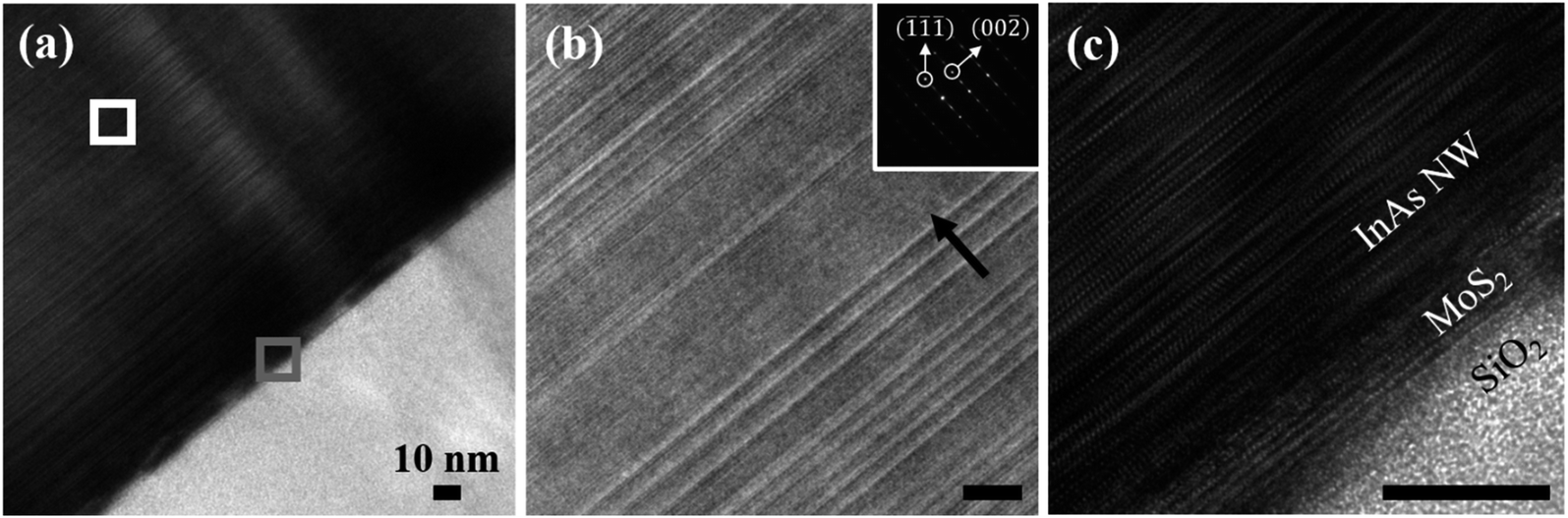 | ||
| Fig. 6 (a–c) HR-TEM images of InAs NW grown under V/III = 25, χTMIn = 8 μmol min−1 and TG = 750 °C. Panel (b) and (c) show higher magnification views of regions highlighted by white and gray borders in panel (a), respectively. A SAED pattern is shown as an inset in (b). The black arrow represents the NW growth direction. | ||
The lattice alignment and in-plane orientation of InAs NWs relative to the triangular MoS2 micro-plates are considered next. Fig. 7(a) shows a plan-view SEM image of a representative InAs NW grown under the optimized SA-vdWE conditions on a triangular MoS2 micro-plate, where the sides of the latter are outlined by white dashed lines. The hexagonally cross-sectioned NW is situated near the center of the MoS2 domain. From the plan-view SEM image, two separate sets of NW sidewall facets (i.e., two families of sidewall planes) can be observed. The sidewall planes can be identified with reference to SAED patterns obtained from NWs lifted out of the as-grown sample using FIB. The interior facets of the NW are principally {2}-oriented, and three of six visible interior facets are aligned in a parallel orientation relative to the three known {100}-oriented sides of the MoS2 micro-plate.49 The exterior NW sidewall facets, however, appear to be rotated 30° relative to the interior facets. Therefore, the exterior facets of the NW are principally {10}-oriented. The legend at the top-right corner of Fig. 7(a) indicates the corresponding directions along the cubic InAs lattice. The apparent rotation of the planar sidewall structure can likely be attributed to the evolution of radially-overgrown NW shell layers upon an axially-grown NW core segment. This stems from preferential adatom nucleation along NW sidewalls, initiated at the low-energy vertices of the core segment sidewalls,50 primarily due to the relative lack of nucleation sites on the vdW surface. Preferential nucleation of adatoms on NW sidewalls leading to modulation of the faceting structure from the {2}-orientation (i.e., central core segment) to the {10}-orientation (i.e., external shell segment) has been previously reported for III–V NWs synthesized under different growth modes.51–55
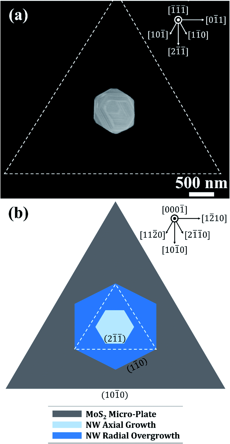 | ||
| Fig. 7 (a) Top-view SEM image of a single InAs NW on a triangular MoS2 domain with micro-plate edges indicated by a dashed white border. (b) Schematic representation of the sidewall faceting structure observed in (a), highlighting the in-plane orientation relationships between the NW core segment (light blue), radially overgrown NW shell segment (dark blue), and triangular MoS2 domain. Cubic and hexagonal lattice directions are indicated by compasses at the top-right corners of (a) and (b), respectively. | ||
A plan-view diagrammatical representation of the in-plane orientation of the axially-grown NW core segment (light blue, interior hexagon) and radially-overgrown NW shell segment (dark blue, exterior hexagon) relative to the triangular MoS2 micro-flake (gray triangle) is shown in Fig. 7(b). The legend at the top-right corner of Fig. 7(b) indicates crystallographic directions corresponding to the hexagonal MoS2 lattice. The representative planar indices of the interior and exterior NW sidewall facets and the exterior MoS2 plate-edge facets are labelled. As a guide to the eye, the white dashed triangular border depicts the coincident sidewall orientations of the NW core segment and the MoS2 micro-flake. Since the NW core segment with {2}-orientated sidewall facets is formed directly on the MoS2 surface, the epitaxial relationship between these two components, which enables vertically-oriented NW growth during SA-vdWE, can be understood in terms of the coincident in-plane alignment of their lattices.
Based on the observed symmetrical orientation and coherent alignment between the NW and 2D micro-plate, a model for a nearly-commensurate super-cell lattice configuration for 〈111〉-oriented InAs NWs on MoS2 is proposed. Fig. 8 depicts the relative atomic arrangement of InAs and MoS2 compounds on equivalent ()- and (000)-oriented surfaces, where Mo-, S-, In-, and As-atoms are shown in blue, yellow, gray, and orange, respectively. The cubic 2 × 2 InAs unit cell is shown as a reference (highlighted by blue borders), along with the primitive unit cell of hexagonal MoS2 (highlighted by red borders). As indicated in Fig. 8, a common sub-lattice is formed such that a distance equal to three multiples of the cubic InAs unit cell along the [2] direction is nearly commensurate with a 14-fold multiple of the Mo–Mo (or S–S) spacing along the [100] direction of the hexagonal lattice. The proposed lattice registry is in agreement with observations based on the top-view SEM image shown in Fig. 7, where the sidewall facets of the InAs core segment are parallel to the MoS2 micro-flake facets.
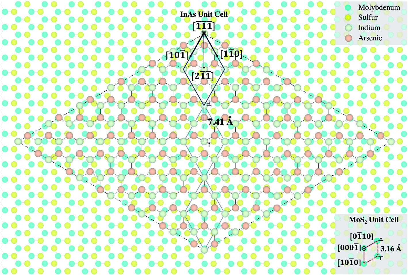 | ||
| Fig. 8 Plan-view model of a nearly-commensurate super-cell configuration composed of a ()-oriented InAs cubic lattice on (000)-oriented MoS2 hexagonal lattice, consistent with the alignment of the NW core segment relative to the MoS2 domain shown in Fig. 7. The 2 × 2 InAs unit cell and MoS2 unit cell are highlighted using blue and red borders, respectively. The legend shows Mo, S, In, and As atoms in blue, yellow, gray, and orange, respectively. A pseudo-commensurate relationship is indicated by 3 multiples of the InAs unit cell in the [2] direction and coincident positions of In and Mo atoms at the corners of the InAs sub-cell, which is shown as the overlaying rhombus-shaped lattice. | ||
Conclusions
In summary, SA-vdWE of vertically aligned InAs NWs on isolated MoS2 domains is demonstrated via MOCVD. The growth parameter space is explored in order to optimize positioning of single InAs NWs on discrete MoS2 micro-plates with one-to-one NW-to-MoS2 placement. The influence of pre-growth surface treatment is examined using PLL. The SA-vdWE growth condition is achieved using a combination of V/III = 25, TG = 750 °C, and χTMIn = 8 μmol min−1 on PLL-treated MoS2 micro-plates. The NWs grown under these conditions exhibit a disordered crystal lattice, similar to the case of vdWE of InAs on graphitic surfaces. Sidewall facet modulation resulting from radial overgrowth on axially-grown NW core segments is observed. The sidewall surfaces of the NW core segment are shown to have a coincident alignment with the MoS2 plate-edges. A model for a nearly-commensurate atomic arrangement of cubic InAs on the hexagonal MoS2 lattice is presented, wherein a three-fold multiple of the cubic InAs unit cell along the [2] direction coincides with a 14-fold multiple of the Mo–Mo (or S–S) spacing along the [100] direction of the MoS2 hexagonal lattice, thereby forming a common sub-lattice. Similar trends are expected for SA-vdWE growth of alternative combinations of III–V compound semiconductor nanostructures and TMDC monolayer materials. The SA-vdWE growth mode enables the synthesis of a new class of mixed-dimensional hybrid nanosystems for heterojunction optoelectronics device applications and quantum communications enabling technologies.
Conflicts of interest
There are no conflicts to declare.Acknowledgements
This material is based upon work supported in part by the National Science Foundation under Award No. 1665086. This work made use of the Cornell Center for Materials Research Shared Facilities which are supported through the National Science Foundation MRSEC program (DMR-1719875). The authors gratefully acknowledge the assistance of Malcolm Thomas and John Grazul in analytical-TEM characterization experiments.References
- D. Jariwala, V. K. Sangwan, L. J. Lauhon, T. J. Marks and M. C. Hersam, ACS Nano, 2014, 8, 1102–1120 CrossRef CAS PubMed.
- K. S. Novoselov, A. K. Geim, S. V. Morozov, D. Jiang, Y. Zhang, S. V. Dubonos, I. V. Grigorieva and A. A. Firsov, Science, 2004, 306, 666–669 CrossRef CAS PubMed.
- J. A. Wilson, F. J. Di Salvo and S. Mahajan, Phys. Rev. Lett., 1974, 32, 882–885 CrossRef CAS.
- G. H. Han, D. L. Duong, D. H. Keum, S. J. Yun and Y. H. Lee, Chem. Rev., 2018, 118, 6297–6336 CrossRef CAS PubMed.
- T. Shishidou, A. J. Freeman and R. Asahi, Phys. Rev. B: Condens. Matter Mater. Phys., 2001, 64, 180401 CrossRef.
- B. Radisavljevic, A. Radenovic, J. Brivio, V. Giacometti and A. Kis, Nat. Nanotechnol., 2011, 6, 147–150 CrossRef CAS PubMed.
- K. Taniguchi, A. Matsumoto, H. Shimotani and H. Takagi, Appl. Phys. Lett., 2012, 101, 042603 CrossRef.
- A. Sajedi-Moghaddam, C. C. Mayorga-Martinez, E. Saievar-Iranizad, Z. Sofer and M. Pumera, Appl. Mater. Today, 2019, 16, 280–289 CrossRef.
- K. A. N. Duerloo, Y. Li and E. J. Reed, Nat. Commun., 2014, 5, 4214 CrossRef CAS PubMed.
- H. Zeng, G. B. Liu, J. Dai, Y. Yan, B. Zhu, R. He, L. Xie, S. Xu, X. Chen, W. Yao and X. Cui, Sci. Rep., 2013, 3, 1608 CrossRef PubMed.
- H. Schmidt, S. Wang, L. Chu, M. Toh, R. Kumar, W. Zhao, A. H. Castro Neto, J. Martin, S. Adam, B. Özyilmaz and G. Eda, Nano Lett., 2014, 14, 1909–1913 CrossRef CAS PubMed.
- A. Splendiani, L. Sun, Y. Zhang, T. Li, J. Kim, C. Y. Chim, G. Galli and F. Wang, Nano Lett., 2010, 10, 1271–1275 CrossRef CAS PubMed.
- T. Li and G. Galli, J. Phys. Chem. C, 2007, 111, 16192–16196 CrossRef CAS.
- A. Splendiani, L. Sun, Y. Zhang, T. Li, J. Kim, C.-Y. Chim, G. Galli and F. Wang, Nano Lett., 2010, 10, 1271–1275 CrossRef CAS PubMed.
- J. Kang, W. Liu and K. Banerjee, Appl. Phys. Lett., 2014, 104, 093106 CrossRef.
- M. Amani, M. L. Chin, A. G. Birdwell, T. P. O'Regan, S. Najmaei, Z. Liu, P. M. Ajayan, J. Lou and M. Dubey, Appl. Phys. Lett., 2013, 102, 193107 CrossRef.
- F. Withers, O. Del Pozo-Zamudio, A. Mishchenko, A. P. Rooney, A. Gholinia, K. Watanabe, T. Taniguchi, S. J. Haigh, A. K. Geim, A. I. Tartakovskii and K. S. Novoselov, Nat. Mater., 2015, 14, 301–306 CrossRef CAS PubMed.
- O. Lopez-Sanchez, D. Lembke, M. Kayci, A. Radenovic and A. Kis, Nat. Nanotechnol., 2013, 8, 497–501 CrossRef CAS PubMed.
- M. L. Tsai, S.-H. Su, J.-K. Chang, D.-S. Tsai, C.-H. Chen, C.-I. Wu, L.-J. Li, L.-J. Chen and J.-H. He, ACS Nano, 2014, 8, 8317–8322 CrossRef CAS PubMed.
- X. Zhou, N. Zhou, C. Li, H. Song, Q. Zhang, X. Hu, L. Gan, H. Li, J. Lü, J. Luo, J. Xiong and T. Zhai, 2D Mater., 2017, 4, 025048 CrossRef.
- M. Long, E. Liu, P. Wang, A. Gao, H. Xia, W. Luo, B. Wang, J. Zeng, Y. Fu, K. Xu, W. Zhou, Y. Lv, S. Yao, M. Lu, Y. Chen, Z. Ni, Y. You, X. Zhang, S. Qin, Y. Shi, W. Hu, D. Xing and F. Miao, Nano Lett., 2016, 16, 2254–2259 CrossRef CAS PubMed.
- L. Ye, H. Li, Z. Chen and J. Xu, ACS Photonics, 2016, 3, 692–699 CrossRef CAS.
- Y. Liu, Y. Huang and X. Duan, Nature, 2019, 567, 323–333 CrossRef CAS PubMed.
- D. Jariwala, T. J. Marks and M. C. Hersam, Nat. Mater., 2017, 16, 170–181 CrossRef CAS PubMed.
- Y. Zhang, J. Wu, M. Aagesen and H. Liu, J. Phys. D: Appl. Phys., 2015, 48, 463001 CrossRef.
- K. Tomioka, M. Yoshimura and T. Fukui, Nature, 2012, 488, 189–192 CrossRef CAS PubMed.
- W. Yang, K. Hu, F. Teng, J. Weng, Y. Zhang and X. Fang, Nano Lett., 2018, 18, 4697–4703 CrossRef CAS PubMed.
- R. Yan, D. Gargas and P. Yang, Nat. Photonics, 2009, 3, 569–576 CrossRef CAS.
- J. C. Shin, P. K. Mohseni, K. J. Yu, S. Tomasulo, K. H. Montgomery, M. L. Lee, J. A. Rogers and X. Li, ACS Nano, 2012, 6, 11074–11079 CrossRef CAS PubMed.
- J. C. Shin, A. Lee, P. Katal Mohseni, D. Y. Kim, L. Yu, J. H. Kim, H. J. Kim, W. J. Choi, D. Wasserman, K. J. Choi and X. Li, ACS Nano, 2013, 7, 5463–5471 CrossRef CAS PubMed.
- S. Plissard, G. Larrieu, X. Wallart and P. Caroff, Nanotechnology, 2011, 22, 275602 CrossRef CAS PubMed.
- K. Tomioka, T. Tanaka, S. Hara, K. Hiruma and T. Fukui, IEEE J. Sel. Top. Quantum Electron., 2011, 17, 1112–1129 CAS.
- E. Bakkers, J. A. van Dam, S. De Franceschi, L. P. Kouwenhoven, M. Kaiser, M. Verheijen, H. Wondergem and P. van der Sluis, Nat. Mater., 2004, 3, 769–773 CrossRef CAS PubMed.
- V. Dhaka, T. Haggren, H. Jussila, H. Jiang, E. Kauppinen, T. Huhtio, M. Sopanen and H. Lipsanen, Nano Lett., 2012, 12, 1912–1918 CrossRef CAS PubMed.
- C. J. Novotny, E. T. Yu and P. K. L. Yu, Nano Lett., 2008, 8, 775–779 CrossRef CAS PubMed.
- A. M. Munshi and H. Weman, Phys. Status Solidi RRL, 2013, 7, 713–726 CrossRef.
- Y. J. Hong and T. Fukui, ACS Nano, 2011, 5, 7576–7584 CrossRef CAS PubMed.
- M. A. Baboli, M. A. Slocum, H. Kum, T. S. Wilhelm, S. J. Polly, S. M. Hubbard and P. K. Mohseni, CrystEngComm, 2019, 21, 602–615 RSC.
- P. K. Mohseni, A. Behnam, J. D. Wood, X. Zhao, K. J. Yu, N. C. Wang, A. Rockett, J. A. Rogers, J. W. Lyding, E. Pop and X. Li, Adv. Mater., 2014, 26, 3755–3760 CrossRef CAS PubMed.
- M. A. Baboli, M. A. Slocum, A. Giussani, S. M. Hubbard and P. K. Mohseni, in 2018 IEEE 18th International Conference on Nanotechnology, IEEE-NANO, 2018, pp. 1–5 Search PubMed.
- Y. J. Hong, W. H. Lee, Y. Wu, R. S. Ruoff and T. Fukui, Nano Lett., 2012, 12, 1431–1436 CrossRef CAS PubMed.
- P. Chen, W. Xu, Y. Gao, P. Holdway, J. H. Warner and M. R. Castell, J. Phys. Chem. C, 2019, 123, 3876–3885 CrossRef CAS.
- U. W. Pohl, Epitaxy of Semiconductors: Introduction to Physical Principles, Springer Science & Business Media, 2013 Search PubMed.
- S. Umehara, N. Pourmand, C. D. Webb, R. W. Davis, K. Yasuda and M. Karhanek, Nano Lett., 2006, 6, 2486–2492 CrossRef CAS PubMed.
- I. N. Yeu, G. Han, C. S. Hwang and J.-H. Choi, Nanoscale, 2020, 12, 17703–17714 RSC.
- K. Tomioka, J. Motohisa, S. Hara and T. Fukui, Nano Lett., 2008, 8, 3475–3480 CrossRef CAS PubMed.
- G. Koblmüller, S. Hertenberger, K. Vizbaras, M. Bichler, F. Bao, J.-P. Zhang and G. Abstreiter, Nanotechnology, 2010, 21, 365602 CrossRef PubMed.
- M. T. Björk, H. Schmid, C. M. Breslin, L. Gignac and H. Riel, J. Cryst. Growth, 2012, 344, 31–37 CrossRef.
- C. Liu, H. Huang, W. Choi, J. Kim, K. Jung, W. Sun, N. Tansu, W. Zhou, H. Kuo and X. Li, ACS Appl. Electron. Mater., 2020, 2, 419–425 CrossRef CAS.
- X. Yin and X. Wang, Nano Lett., 2016, 16, 7078–7084 CrossRef CAS PubMed.
- M. C. Plante and R. R. LaPierre, J. Cryst. Growth, 2008, 310, 356–363 CrossRef CAS.
- N. Sköld, J. B. Wagner, G. Karlsson, T. Hernán, W. Seifert, M.-E. Pistol and L. Samuelson, Nano Lett., 2006, 6, 2743–2747 CrossRef PubMed.
- Q. Zhang, J.-N. Aqua, P. W. Voorhees and S. H. Davis, J. Mech. Phys. Solids, 2016, 91, 73–93 CrossRef CAS.
- I. Yang, X. Zhang, C. Zheng, Q. Gao, Z. Li, L. Li, M. N. Lockrey, H. Nguyen, P. Caroff, J. Etheridge, H. H. Tan, C. Jagadish, J. Wong-Leung and L. Fu, ACS Nano, 2018, 12, 10374–10382 CrossRef CAS PubMed.
- T. Xu, K. A. Dick, S. Plissard, T. H. Nguyen, Y. Makoudi, M. Berthe, J.-P. Nys, X. Wallart, B. Grandidier and P. Caroff, Nanotechnology, 2012, 23, 095702 CrossRef PubMed.
Footnote |
| † Electronic supplementary information (ESI) available. See DOI: 10.1039/d0na00768d |
| This journal is © The Royal Society of Chemistry 2021 |