DOI:
10.1039/D0NA00759E
(Paper)
Nanoscale Adv., 2021,
3, 1127-1135
Anomalous plasmons in a two-dimensional Dirac nodal-line Lieb lattice†
Received
9th September 2020
, Accepted 24th December 2020
First published on 26th December 2020
Abstract
Plasmons in two-dimensional (2D) Dirac materials feature an interesting regime with a tunable frequency, and long propagating length and lifetime, but are rarely achieved in the visible light regime. Using a tight-binding (TB) model in combination with first-principles calculations, we investigated plasmon modes in a 2D Lieb lattice with a Dirac nodal-line electronic structure. In contrast to conventional 2D plasmons, anomalous plasmons in the Lieb lattice exhibit the unique features of a carrier-density-independent frequency, being Landau-damping free in a wide-range of wave vectors, a high frequency, and high subwavelength confinement. Remarkably, by using first-principles calculations, we proposed a candidate material, 2D Be2C monolayer, to achieve these interesting plasmon properties. The plasmons in the Be2C monolayer can survive up to the visible frequency region and propagate to large momentum transfer that has rarely been reported. The anomalous plasmons revealed in the Lieb lattice offer a promising platform for the study of 2D plasmons as well as the design of 2D plasmonic materials.
Introduction
Plasmons, as collective excitations of electrons, enable coupling between electromagnetic radiation and electrons in materials at subwavelength scales, and a wide-range of applications, such as photodetection, biosensing and nanophotonics.1–7 The dimensionality of materials offers additional freedom to regulate plasmonic properties,8–12 among which two-dimensional (2D) materials are of particular interest, due to their unique electronic structures and quantum-confinement effects.13–22 For example, plasmons in graphene have been demonstrated to possess high tunability, large subwavelength confinement and a longer propagating length and lifetime both theoretically and experimentally.2,18,19 These plasmonic properties are closely related to the unique linear energy–momentum dispersion relation in graphene, namely Dirac cones. Additionally, the exotic electronic structures of topological materials, such as topological insulators (TI)23 and topological semimetal (TSM) states,24 offer a new platform for creating plasmons, revealing a series of interesting scenarios. Recently, a novel undamped gapless plasmon mode was predicted in a type-II Dirac semimetal, benefitting from the presence of both electron and hole pockets at the Fermi surface due to the titled Dirac cone.25 The plasmon properties of three-dimensional (3D) Dirac nodal line (DNL) semimetals with a nodal line Fermi ring formed by band touching points have also been investigated. In the long-wavelength limit, the plasmon frequency (ωp) shows a special dependence on the carrier density (n), ωp ∝ n1/4,26,27 which differs significantly from the ωp ∝ n1/2 law in 3D metals, 2D electron gas28 and bilayer graphene,29 but similar to that of graphene.18 The carrier-density-dependent plasmon frequency offers a simple strategy to regulate the plasmon properties, e.g. by doping or the gate voltage. However, it is unsuitable for applications where stable plasmons against environment perturbation are required. It is also disadvantageous for improving the plasmon density at a low frequency and the lifetime at high carrier density.30 Very recently, anomalous plasmons with a density-independent frequency, intensity and damping were predicted in one-dimensional topological electrides with Dirac nodal-surface states,30 paving a way for the design of plasmonic materials.
Another key parameter of plasmons is the maximal frequency of undamped plasmon modes, which is determined by the edges of single-particle excitation (SPE) continuum. As the collective mode enters the SPE continuum, it will be damped and decay into electron–hole pairs. Typically, plasmons in gate-doped graphene emerge only in the infrared to terahertz range,31–33 due to the confinement of SPE continuum. To date, very few plasmons with the frequency in the visible range have been predicted in 2D materials.21
Here, we investigated the plasmon excitation spectrum in a 2D DNL semimetal by using a tight-binding model in combination with first-principles calculations. We demonstrated that the 2D DNL states in the Lieb lattice can lead to anomalous plasmons with a stable frequency independent of the carrier density n, in sharp contrast to normal plasmons in 2D materials, such as graphene.2,18,19 Moreover, anomalous 2D plasmons are Landau-damping free in a wide-range of wave vectors, and have a high frequency, and high subwavelength confinement. We proposed a simple two-band model to interpret the density-independent frequency of plasmons. More interestingly, the SPE continuum can be effectively regulated by controlling the carrier density, to yield long-lived plasmons. Using first-principles calculations, we proposed a candidate material, 2D Be2C monolayer,34 to realize these interesting plasmons. Our calculations showed that the plasmons in the Be2C monolayer can survive up to the visible frequency region and propagate to large momentum transfer that has rarely been reported. Additionally, acoustic plasmon (AP) modes, characterized by linear dispersion in small momentum transfer, emerge in the electron-doped Be2C monolayer. The intensity and momentum transfer of these AP modes are much higher than those predicted in doped graphene19,35 and other 2D materials36,37 and thus likely detectable in experiments. Anomalous plasmons in the Lieb lattice hold great promise for the design of plasmonic devices.
Methods and computational details
A. Random-phase approximation
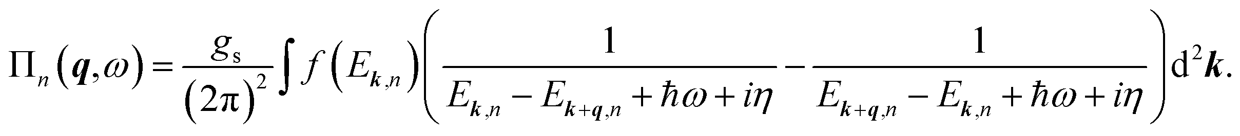
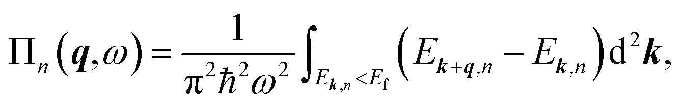
Under the random-phase approximation (RPA) approach, the polarization function reads38,39| | 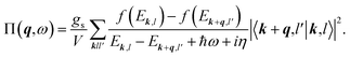 | (1) |
here gs = 2 is the spin degeneracy, V is the area of the two-dimensional system, the broadening parameter is taken to be η, and the Fermi distribution function denoted by f(E) acts as a step function at T = 0. Ekl and |k,l〉 are respectively the eigenvalues and eigenstates of the Hamiltonian matrix, where l represents the band indice. The dielectric function ε(q,ω) was determined from the polarization function using the equation:| | | ε(q,ω) = 1 − VqΠ(q,ω), | (2) |
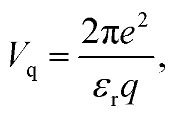
where Vq is the Fourier transform of the Coulomb potential and can be written for a 2D system as| |  | (3) |
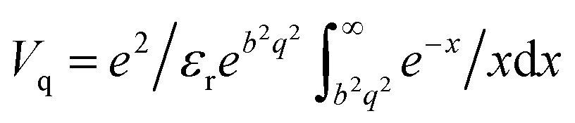
Notably, Vq is highly dependent on the dimensionality of the materials and becomes Vq = 4πe2/(εrq2) for 3D materials, and 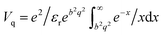 for 1D materials,40 where εr is the background dielectric constant, and b is the width of the 1D materials. The dynamical loss function, which is related to the momentum-resolved electron energy loss spectrum (EELS), can be expressed as
| | | εloss(q,ω) = −Im[1/ε(q,ω)]. | (4) |
The plasmon is characterized by the peak of the dynamical loss function.
B. First-principles calculations
Our first-principles calculations were performed using density functional theory, as implemented in the Vienna ab initio simulation package (VASP)41 and GPAW codes,42 which both employ the projector augmented-wave method43 to model interactions between electrons and ions with an energy cutoff of 500 eV. The generalized gradient approximation44 in the form of Perdew–Burke–Ernzerhof45 was adopted for the exchange–correlation functional. A vacuum space of 20 Å was used along the z-direction to exclude the interaction between neighbouring images. Structure relaxation and electronic properties were calculated using VASP on the 13 × 13 × 1 k-point mesh. The lattice constants and the atomic positions were fully relaxed until the atomic forces on the atoms were less than 0.01 eV Å−1 and the total energy change was less than 10−5 eV. The electron doping effect was simulated by adding or extracting extra electrons to the lattices in a homogeneous background charge of opposite sign. The band structures on the basis of maximally localized Wannier functions (MLWFs) were determined using WANNIER90 package.46
The dynamic dielectric function and loss function were performed using linear response calculations47 as implemented in the GPAW code. A denser k-point grid of 61 × 61 × 1 was used to include and accurate description of intra-band transitions. The dielectric matrix for in-plane wave vector q was calculated in random phase approximation (RPA) as:47
| |  | (5) |
We consider up to 40 empty bands to describe the response function. A cut-off of 50 eV for reciprocal lattice vectors and a broadening parameter η = 0.05 eV were used to account for local field effects. In order to avoid the interaction between the periodic replicas, a 2D truncated Coulomb kernel was taken.48
Results and discussion
A. Two-band model of a 2D DNL
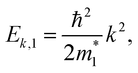
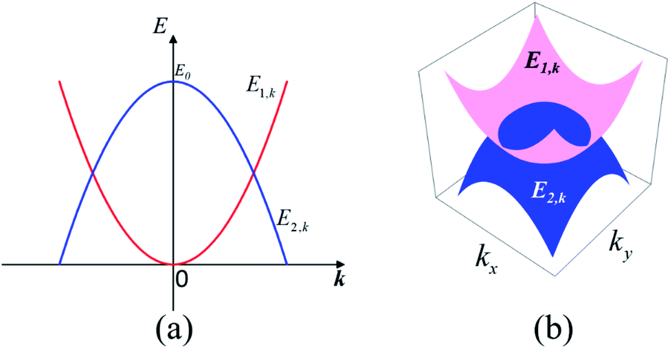
We started from a simple model for the DNL in 2D materials to demonstrate the possibility of carrier-density-independent plasmons. We supposed that the DNL is formed from two crossing bands described by parabolic dispersion relations as follows:| |  | (6) |
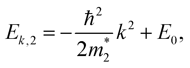
| | 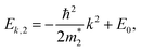 | (7) |
with the effective masses  and E0 > 0, as shown in Fig. 1. Assuming that the electron wavefunctions of the two bands are orthogonal (e.g. they arise from pz and pxy orbitals, respectively), the inter-band transition of electrons is prohibited.
 |
| | Fig. 1 (a) Schematic representation of the two-band model of the 2D DNL formed from the cross of two parabolic bands. (b) The profiles of the 2D DNL in the reciprocal space. | |
The intra-band contribution of band n to the polarization functions reads:
| |  | (8) |
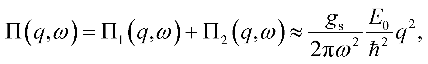
Under the long-wavelength limit, it can be reduced to:
| |  | (9) |
as the Fermi level
Ef varies from 0 to
E0. From
eqn (9), we got the polarization function (see Sec. S2 of the ESI for more details
†):
| |  | (10) |
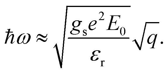
and the dispersion of the plasmon mode of this system:
| |  | (11) |
Notably, the plasmon spectrum is independent of the Fermi level (carrier density) and the effect masses of electrons.
B. Tight-binding model for 2D plasmons in a Lieb lattice
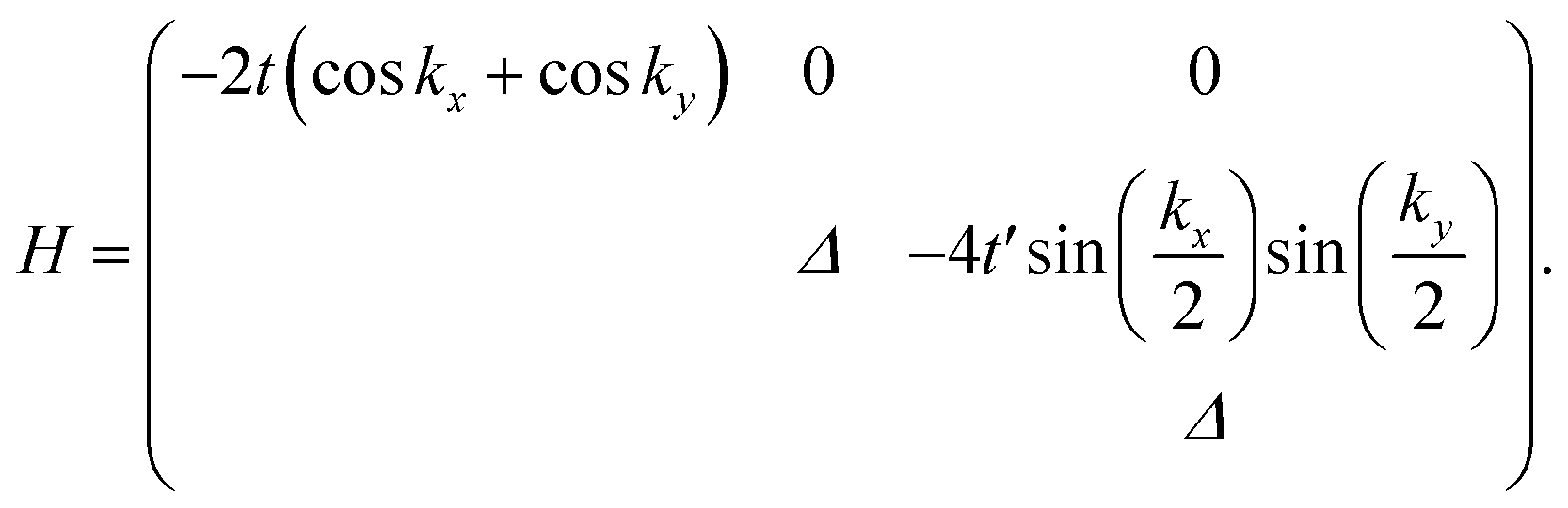
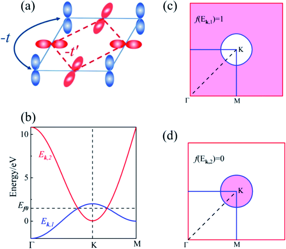
We then considered the DNL in the 2D Lieb lattice proposed in our previous work,34 as shown in Fig. 2(a). The Lieb lattice is composed of two square sublattices of pz and px,y orbitals, respectively. Electron hopping between adjacent sites is prohibited due to the orthogonal feature between pz and px,y orbitals. Therefore, only electron hopping within the sublattices characterized by −t and −t′ (t > 0, t′ > 0) was taken into account in our tight-binding (TB) Hamiltonian:| |  | (12) |
Here, Δ represents the on-site energy difference between two sublattices. Spin–orbit coupling (SOC) was not taken in account.
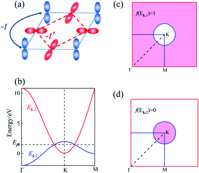 |
| | Fig. 2 Tight-binding model of the 2D p-orbital Lieb lattice with a Dirac nodal-line electronic structure. (a) Lieb lattice of pz and px,y orbitals. (b) The lower two bands of the TB model, Ek,1 and Ek,2, with t = 0.5 eV, t′ = 2.7 eV, Δ = 10.84 eV. (c and d) The Brillouin zone of the Lieb lattice. The shaded areas in (c) and (d) represent the momentum regions of Ek,1 < Ef0 and Ek,2 < Ef0, respectively. | |
The lower two bands, Ek,1 and Ek,2 of the TB Hamiltonian,
| | Ek,1 = −2t(cos![[thin space (1/6-em)]](https://www.rsc.org/images/entities/char_2009.gif) kx + cosky), kx + cosky), | (13) |
| |  | (14) |
cross and form a Dirac nodal-line (DNL) centered at the
K point, as (
t +
t′) >
Δ/4. Assuming that there are two residual electrons per unit cell, the Fermi level
Ef0 is right at the band touching points, as shown in
Fig. 2(b). The eigenvectors of the two bands are contributed respectively from the p
z and p
x,y orbitals and thus orthogonal to each other. The inter-band excitation of electrons between the two bands is forbidden and thus the contribution of inter-band transition to the polarization function can be omitted, similar to the case of the above two-band model.
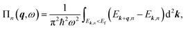
In the long-wavelength limit, the polarization function can be evaluated as follows:
| |  | (15) |
Here
Ω1 and
Ω2 represent the momentum regions of
Ek,1 <
Ef and
Ek,2 <
Ef, as shown by the shaded areas in
Fig. 2(c and d), respectively. The plasmon dispersion identified as the roots of
ε(
q,
ω) = 0 can be reduced approximated to
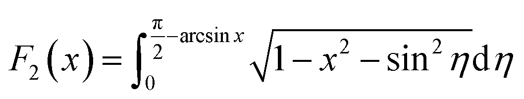
| |  | (16) |
with
and
,
(see Sec. S3 of the ESI for more details
†). The plasmon modes are isotropic and satisfies
ω ∝
q1/2 in the long-wavelength limit, similar to that of 2D electron gas.
28
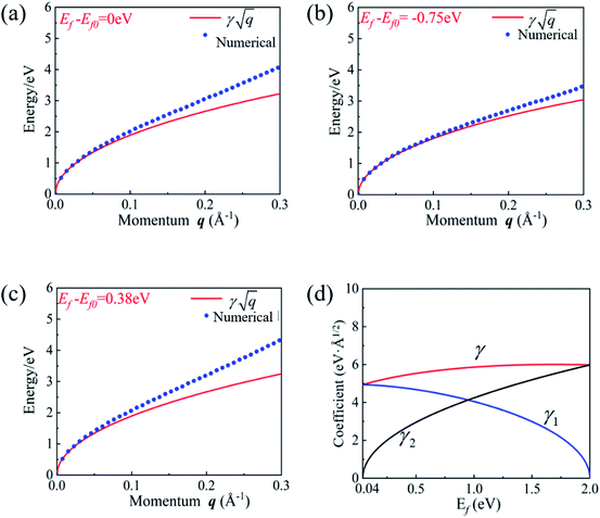
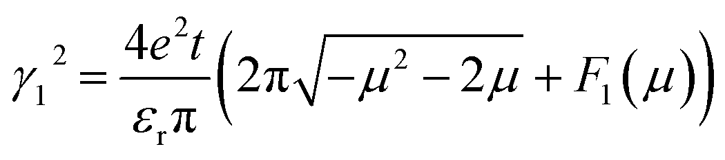
We also calculated the plasmon spectra using eqn (8)via numerical integration without long-wavelength approximation. The plasmon spectra along the Γ–M direction of the Lieb lattice with different Fermi energy (Ef) are plotted in Fig. 3(a–c). Obviously, the data obtained directly from eqn (16) agree well with those from numerical calculations in the long wavelength region. Notably, both μ and ν are dependent on the Fermi level Ef. The dependence of γ on the Fermi level was plotted in Fig. 3(d). As the Fermi level is pushed from the bottom of Ek,2 (0.04 eV) to the top of Ek,1 (2.0 eV), γ changes slightly from 4.93 to 6.0 eV Å1/2. This scenario differs significantly from that of traditional 2D systems,18,28,29 whose frequency strongly depends on carrier density, and reflects the unique characteristics of the 2D DNL. This TB model is also consistent with the two-band model, in which the energy difference between the bottom of Ek,2 and the top of Ek,1 is E0 = 1.96 eV. According to eqn (11), we have γ = 6.13 eV Å1/2, which is very close to the values (4.93–6.0 eV Å1/2) obtained from the TB model.
 |
| | Fig. 3 (a–c) The energy spectra of plasmons along the Γ–M direction for three different Fermi levels obtained by eqn (16) (solid red lines) and numerical calculations of eqn (8) without the long-wavelength limit (blue dots). (d) The relationship between the coefficient γ(γ1,γ2) and Fermi level Ef as the Fermi level was pushed from the bottom of Ek,2 (0.04 eV) to the top of Ek,1 (2.0 eV). The TB parameters are listed in Sec. S4 of the ESI.† | |
In order to reveal the relation between γ and Ef, we divided γ as γ2 = γ12 + γ22, with  and
and  . Here, γ1 and γ2 represent the contributions of Ek,1 and Ek,2, respectively. The variation of γ1 and γ2 as a function of Fermi energy is plotted in Fig. 3(d). As Ef increases from the bottom of the band Ek,2 to the top of the band Ek,1, γ1 gradually decreases and finally becomes zero when Ef reaches the top of the band Ek,1, while γ2 shows an opposite trend. As a result, γ becomes insensitive to the Fermi energy (or carrier density).
C. 2D plasmons in the Be2C monolayer
To achieve anomalous plasmons in realistic materials, we considered a 2D Be2C monolayer proposed in our previous work.34 The Be2C monolayer possesses a line-centered square (Lieb) lattice with a lattice constant of 3.276 Å, where Be and C reside at the line-center and vertex sites, respectively, as shown in Fig. 4(a). The stability and plausibility of the Be2C monolayer have been verified from first-principles calculations.34 From the orbital-resolved electronic band structure plotted in Fig. 4(b), one can see clearly that the two bands cross along the M–K and Γ–K directions right at the Fermi level, forming a nodal ring centered at the K point. The two bands near the Fermi level are contributed mainly by the px,y orbitals of Be atoms and the pz orbital of C atoms, respectively, meeting the requirement of the above models. Therefore, the 2D Be2C monolayer may serve as a promising candidate material to realize anomalous plasmons predicted by the two-band model and TB model.
 |
| | Fig. 4 (a) The Lieb lattice of the Be2C monolayer. (b) The orbital-resolved band structure of the Be2C monolayer. The 3D band structure near the K point is shown in the inset. (c) Comparison of the band structure obtained from DFT methods (solid red lines) and MLWFs (dash-dotted black lines). Green dotted lines show the position of the Fermi level at different doping levels. (d) Imaginary part of the dielectric function of the pristine and doped Be2C monolayer. Black dotted lines show an approximate linear fit used to estimate the threshold energy of inter-band transitions. | |
We also plotted the band structure of the Be2C monolayer on the basis of maximally localized Wannier functions (MLWFs), which matches well with the DFT results in the energy range of [−5, 2] eV, as shown in Fig. 4(c). To mimic the effect of regulating the Fermi level, we doped holes (or electrons) into the Be2C monolayer with a concentration of 4.66 × 1014 cm−2. Compared with pristine Be2C, the Fermi level is pushed downward (or upward) by 0.75 eV (or 0.38 eV). The Dirac nodal-line states are still robust against doping (see Fig. S2 of the ESI†).
Notably, the two bands that form the DNL states near the Fermi level originate from different atomic orbitals: the px,y orbitals of Be atoms and the pz orbital of C atoms. Electron excitation between the two bands (inter-band excitation) is not allowed due to the different symmetries of the two orbitals. This feature can be verified from the imaginary part of the dielectric function (Imε) which describes the optical adsorption spectra of materials. Our first-principles calculations showed that the adsorption spectrum of pristine of Be2C has a threshold energy of about 3.13 eV, below which the inter-band excitation of electrons is prohibited, as shown in Fig. 4(d). For the hole- (or electron-) doped Be2C monolayer, the threshold energy becomes 2.62 eV (or 3.42 eV) at the doping concentration of 4.66 × 1014 cm−2. The threshold energy in the optical adsorption spectra of the DNL semimetallic Be2C monolayer is consistent with the theoretical models proposed in the previous sections and responsible for the anomalous plasmons.
The plasmon dispersion curves of the Be2C monolayer along the Γ–M direction in the energy range of 0–4 eV are shown in Fig. 5, which were extracted from the peaks of EELS. The plasmon mode indicated by the red circles was named Dirac Plasmon (DP), because it originates from the collective electronic excitations of the Dirac nodal-line. For the small momentum transfer up to around 0.06 Å−1, the plasmon spectrum of the Be2C monolayer obtained from DFT calculations is in good agreement with the results of the TB model, which follows the universal long wavelength  behavior of 2D electron gas.49 But for large momentum transfer q, it deviates gradually from the
  rule. We ascribed it to the origins of the plasmons in the Be2C monolayer. In the small momentum region, the plasmons are mainly dominated by the intra-band transition of the two DNL bands. With the increase of momentum, however, the inter-band transition comes to occur and contributes to the polarization function. The consequent screening effect results in the redshift of the plasmon energy and deviation from the TB model.22 From the plasmon spectra under these three different doping conditions in Fig. 5(a), we can see that γ is nearly insensitive to the Fermi level. For further verification, we fitted the plasmon spectra of the Be2C monolayers in the low energy region by eqn (16) and got γ = 5.63 Å1/2 and 5.74 eV Å1/2 for the hole- and electron-doped Be2C monolayers with a concentration of 4.66 × 1014 cm−2, respectively, which are very close to that of the pristine Be2C monolayer, 5.76 eV Å1/2, in good agreement with the TB model.
 |
| | Fig. 5 (a) Comparation of plasmon energy at different doping. Plasmon dispersion of the (b) pristine, (c) hole-doped and (d) electron-doped Be2C monolayer along the Γ–M direction. Red circles are results from DFT methods and the diameter of the circles is proportional to ln{Im[ε]}, indicating the strength of the plasmon mode. The results from MLWFs (blue dots) and analytical  dispersion (solid black lines) are also shown for comparison. The shaded areas indicate the SPE regions due to inter-band (yellow) and intra-band (green) transitions, respectively. dispersion (solid black lines) are also shown for comparison. The shaded areas indicate the SPE regions due to inter-band (yellow) and intra-band (green) transitions, respectively. | |
To further include the contribution of other atomic orbitals, we also adopted a more complicated TB model by involving s- and p-orbitals in each site of the Lieb lattice to describe the electronic band structure and plasmonic properties of the Be2C monolayer. The parameters of the TB model can be obtained from the MLWF strategy by reproducing the band structure of the Be2C monolayer, as shown in Fig. 4(c). The plasmon modes calculated from the TB model agree well with the results of DFT calculations in the whole momentum region, as shown in Fig. 5(b–d).
Single-particle excitations (SPEs), due to intra-band and inter-band excitation (also known as Landau damping) dominate the plasmon damping processes. The SPE continuum is defined by the nonzero value of the imaginary part of the polarizability function, ImΠ(q,ω).18 In our system, the borders of intra-band and inter-band SPE continuum can be determined approximately by ℏ2q2/2m + ℏvFq and ℏ2q2/2m + ℏωSPE − ℏvF2q, respectively, in which ℏ2q2/2m is negligible compared with other terms as q → 0.18,50,51vF represents the maximal electron velocity of the band across the Fermi level, which was set to 1.13 × 10⁶ m s−1, 0.85 × 10⁶ m s−1 and 1.14 × 10⁶ m s−1 for the pristine, hole-doped and electron-doped Be2C monolayer, respectively, according to our DFT calculations. vF2 is the electron velocity of the nearly flat band at around −3.5 eV in Fig. 4(c), which is responsible for the start of inter-band excitation. Our calculations showed that vF2 is insensitive to electron- or hole-doping and the maximum value of vF2 is about 1.9 × 10⁵ m s−1. The inter-band threshold frequency ωSPE was identified as 3.13 eV, 2.62 eV, and 3.42 eV for pristine, hole-doped and electron-doped Be2C, respectively. Remarkably, the carrier-density-dependent ωSPE is quite crucial for regulating the SPE continuum to achieve high-frequency plasmons. The shaded regions in Fig. 5(b–d) depict the SPE regions. When the plasmon mode hits the SPE continuum, it becomes damped and decays into electron–hole pairs. For pristine Be2C in Fig. 5(b), the plasmons are undamped up to 2.88 eV (q < 0.33 Å−1). In the hole-doped Be2C monolayer, the SPE continuum moves downward, as shown in Fig. 5(c), and the maximal frequency of the undamped plasmons decreases to 2.14 eV (q < 0.25 Å−1). In contrast, in the electron-doped Be2C monolayer, the improved ωSPE raises the boundary of the inter-band SPE region, making the plasmons extend up to 3.10 eV (q < 0.37 Å−1), as shown in Fig. 5(d). Notably, the 2D plasmons in the visible frequency range remain challenging. Anomalous plasmons predicted in the Be2C monolayer offer a promising approach to reach this goal.
Another interesting scenario worth noting is that, for the electron-doped Be2C monolayer, a new type of plasmon mode emerges, which has a linear dispersion and coincides with the intra-band SPE boundary in small momentum transfer, as indicated by blue circles in Fig. 5(d). A similar plasmon mode defined as acoustic plasmon (AP) has been predicted in doped-graphene,19,35 but the intensity is too low. For the AP mode in the Be2C monolayer, however, the intensity is greatly enhanced in the high q region, and even exceeds the intensity of the DP. Although the AP mode enters into the electron–hole excitation area at seemingly small q (∼0.1 Å−1), the high intensity and relatively larger momentum transfer than other 2D materials like doped-graphene make it detectable in experiments.
To verify the collective excitation features (rather than single-particle resonances) of the two-types of plasmon modes (DP and AP), we plotted the dielectric functions and loss functions of the Be2C monolayer at q = 0.063 Å−1 in Fig. 6. Collective excitation should fulfill Reε = 0 with Imε/∂ωReε > 0 at the energy where the peak of loss function occurs. If the Imε presents a vanishing small value in the same energy region, the plasmon is undamped and lies out of the SPE regions.25,52,53 From Fig. 6 we can clearly see that, all conditions are fulfilled in the DP case, confirming the plasmonic nature of the DP mode. For the electron-doped Be2C monolayer, Imε deviates slightly from zero at the energy where AP occurs. We attribute it to the artificial broadening effect of the two peaks in the Imε spectrum in our DFT calculations.
 |
| | Fig. 6 (a–c) Dielectric function and loss function of pristine, hole-doped and electron-doped Be2C monolayers at q = 0.063 Å−1. The upper panel is the real (blue solid lines) and imaginary part (red dashed lines) of the dielectric function, and the blue circles denote the zeros of Reε(q,ω) corresponding to collective excitations. The lower panel is the corresponding loss function, in which the DP and AP modes are marked near the peaks. (d–f) Wave localization of the DP mode in pristine, hole-doped and electron-doped Be2C monolayers, respectively. The shaded areas correspond to SPE damping regions. | |
We finally evaluate the wave localization (or wave shrinkage) of the DP in the Be2C monolayer from the confinement of the wavelength of a plasmon mode. Wave localization is qualified as λair/λp, in which λp = 2π/q is the wavelength of a plasmon wave and λair = 2πc/ω is the corresponding wavelength in air. The maximum wave localization of the undamped plasmons was determined to be 228, 231 and 213 for the pristine, hole-doped and electron-doped Be2C monolayer, respectively, as illustrated in Fig. 6(d–f). These values are larger than those predicted in doped-graphene (100–200)54 and bulked triangular 2D boron (∼150),21 demonstrating the subwavelength confinement of the plasmons in the Be2C monolayer which would be beneficial for miniaturization of plasmonic devices and savings of the operational power.55
We should mention that achieving visible-range plasmons in 2D materials remains challenging in experiments.56 For gate-doped graphene, plasmons can emerge in the terahertz to infrared range, which has been proved both theoretically and experimentally.2,18,19,31–33 Electron-doping was predicted to extend the frequency of 2D plasmons to the infrared region in MoS2 monolayers.57 Through electrochemically intercalating lithium into MoS2 nanoflakes, plasmon resonances in the visible and near UV wavelength ranges were realized in recent experiments.58 In present work, we predicted that the plasmon mode in the Be2C monolayer can extend to the visible range, even without doping, offering an alternative approach to achieve visible-range plasmons in 2D materials.
Conclusions
In summary, we revealed anomalous plasmons inherited in the Lieb lattice with DNL electronic structures using a TB model in combination with first-principles calculations. Our study showed that the plasmons exhibit the unique features of a density-independent frequency, being Landau-damping free in a wide-range of wave vectors, a high frequency, and high subwavelength confinement, which can be attributed to the DNL states and symmetry-restricted inter-band excitation. The SPE continuum can be effectively regulated by controlling the carrier density, yielding long-lived plasmons. These interesting plasmonic properties can be realized in a 2D Be2C monolayer. More interestingly, acoustic plasmon (AP) modes, characterized by linear dispersion in small momentum transfer, emerge in the electron-doped Be2C monolayer. The intensity and momentum transfer of these AP modes is comparable to that of the DP modes and thus has high possibility to be detected in experiments. Our work is expected to offer a promising strategy for achieving stable plasmons in the visible light regime.
Conflicts of interest
There are no conflicts to declare.
Acknowledgements
The National Key Research and Development Program of China (no. 2016YFA0301200); National Natural Science Foundation of China (No. 11774201); Taishan Scholar Program of Shandong Province.
References
- S. V. Boriskina, H. Ghasemi and G. Chen, Mater. Today, 2013, 16, 375 CrossRef CAS.
- J. Chen, M. Badioli, P. Alonso-Gonzalez, S. Thongrattanasiri, F. Huth, J. Osmond, M. Spasenovic, A. Centeno, A. Pesquera, P. Godignon, A. Z. Elorza, N. Camara, F. J. Garcia de Abajo, R. Hillenbrand and F. H. Koppens, Nature, 2012, 487, 77 CrossRef CAS.
- K. M. Mayer and J. H. Hafner, Chem. Rev., 2011, 111, 3828 CrossRef CAS.
- Z. Torbatian and R. Asgari, Appl. Sci., 2018, 8, 238 CrossRef.
- V. J. Sorger, R. F. Oulton, R.-M. Ma and X. Zhang, MRS Bull., 2012, 37, 728 CrossRef CAS.
- H. A. Atwater and A. Polman, Nat. Mater., 2010, 9, 205 CrossRef CAS.
- C. Clavero, Nat. Photonics, 2014, 8, 95 CrossRef CAS.
- E. P. Rugeramigabo, C. Tegenkamp, H. Pfnür, T. Inaoka and T. Nagao, Phys. Rev. B: Condens. Matter Mater. Phys., 2010, 81, 165407 CrossRef.
- T. Nagao, S. Yaginuma, T. Inaoka and T. Sakurai, Phys. Rev. Lett., 2006, 97, 116802 CrossRef.
- K. Andersen, K. W. Jacobsen and K. S. Thygesen, Phys. Rev. B: Condens. Matter Mater. Phys., 2014, 90, 161410 CrossRef.
- P. Di Pietro, M. Ortolani, O. Limaj, A. Di Gaspare, V. Giliberti, F. Giorgianni, M. Brahlek, N. Bansal, N. Koirala, S. Oh, P. Calvani and S. Lupi, Nat. Nanotechnol., 2013, 8, 556 CrossRef CAS.
- T. Stauber, J. Phys.: Condens. Matter, 2014, 26, 123201 CrossRef.
- C. Lewandowski and L. Levitov, Proc. Natl. Acad. Sci. U. S. A., 2019, 116, 20869 CrossRef CAS.
- T. Zhou, J. Zhang, H. Jiang, I. Žutić and Z. Yang, npj Quantum Mater., 2018, 3, 39 CrossRef.
- X. Zhang, Z. Wang, M. Zhao and F. Liu, Phys. Rev. B: Condens. Matter Mater. Phys., 2016, 93, 165401 CrossRef.
- M. Koshino, N. F. Q. Yuan, T. Koretsune, M. Ochi, K. Kuroki and L. Fu, Phys. Rev. X, 2018, 8, 031087 CAS.
- H. Gao and W. Ren, Carbon, 2020, 158, 210 CrossRef CAS.
- E. H. Hwang and S. Das Sarma, Phys. Rev. B: Condens. Matter Mater. Phys., 2007, 75, 205418 CrossRef.
- Y. Gao and Z. Yuan, Solid State Commun., 2011, 151, 1009 CrossRef CAS.
- B. Ghosh, P. Kumar, A. Thakur, Y. S. Chauhan, S. Bhowmick and A. Agarwal, Phys. Rev. B: Condens. Matter Mater. Phys., 2017, 96, 035422 CrossRef.
- Y. Huang, S. N. Shirodkar and B. I. Yakobson, J. Am. Chem. Soc., 2017, 139, 17181 CrossRef CAS.
- K. Andersen and K. S. Thygesen, Phys. Rev. B: Condens. Matter Mater. Phys., 2013, 88, 155128 CrossRef.
- M. Xu, G. Zhan, S. Liu, D. Zhang, X. Zhong, Z. Qu, Y. Li, A. Du, H. Zhang and Y. Wang, Phys. Rev. B: Condens. Matter Mater. Phys., 2019, 100, 235435 CrossRef CAS.
- H. Huang, W. Jiang, K.-H. Jin and F. Liu, Phys. Rev. B: Condens. Matter Mater. Phys., 2018, 98, 045131 CrossRef CAS.
- K. Sadhukhan, A. Politano and A. Agarwal, Phys. Rev. Lett., 2020, 124, 046803 CrossRef CAS.
- Z. Yan, P.-W. Huang and Z. Wang, Phys. Rev. B: Condens. Matter Mater. Phys., 2016, 93, 085138 CrossRef.
- J.-W. Rhim and Y. B. Kim, New J. Phys., 2016, 18, 043010 CrossRef.
- F. Stern, Phys. Rev. Lett., 1967, 18, 546 CrossRef CAS.
- R. Sensarma, E. H. Hwang and S. Das Sarma, Phys. Rev. B: Condens. Matter Mater. Phys., 2010, 82, 195428 CrossRef.
- J. Wang, X. Sui, S. Gao, W. Duan, F. Liu and B. Huang, Phys. Rev. Lett., 2019, 123, 206402 CrossRef CAS.
- A. N. Grigorenko, M. Polini and K. S. Novoselov, Nat. Photonics, 2012, 6, 749 CrossRef CAS.
- H. Yan, T. Low, W. Zhu, Y. Wu, M. Freitag, X. Li, F. Guinea, P. Avouris and F. Xia, Nat. Photonics, 2013, 7, 394 CrossRef CAS.
- D. Rodrigo, O. Limaj, D. Janner, D. Etezadi, F. J. García de Abajo, V. Pruneri and H. Altug, Science, 2015, 349, 165 CrossRef CAS.
- B. Yang, X. Zhang and M. Zhao, Nanoscale, 2017, 9, 8740 RSC.
- P. Alonso-González, A. Y. Nikitin, Y. Gao, A. Woessner, M. B. Lundeberg, A. Principi, N. Forcellini, W. Yan, S. Vélez, A. J. Huber, K. Watanabe, T. Taniguchi, F. Casanova, L. E. Hueso, M. Polini, J. Hone, F. H. L. Koppens and R. Hillenbrand, Nat. Nanotechnol., 2017, 12, 31 CrossRef.
- P. Li, X. Ren and L. He, Phys. Rev. B: Condens. Matter Mater. Phys., 2017, 96, 165417 CrossRef.
- Z. Torbatian and R. Asgari, J. Phys.: Condens. Matter, 2017, 29, 465701 CrossRef CAS.
- S. L. Adler, Phys. Rev., 1962, 126, 413 CrossRef.
- N. Wiser, Phys. Rev., 1963, 129, 62 CrossRef.
- C. Lian, S. Q. Hu, J. Zhang, C. Cheng, Z. Yuan, S. Gao and S. Meng, Phys. Rev. Lett., 2020, 125, 116802 CrossRef CAS.
- G. Kresse and J. Furthmüller, Phys. Rev. B: Condens. Matter Mater. Phys., 1996, 54, 11169 CrossRef CAS.
- J. Enkovaara, C. Rostgaard, J. J. Mortensen, J. Chen, M. Dułak, L. Ferrighi, J. Gavnholt, C. Glinsvad, V. Haikola, H. A. Hansen, H. H. Kristoffersen, M. Kuisma, A. H. Larsen, L. Lehtovaara, M. Ljungberg, O. Lopez-Acevedo, P. G. Moses, J. Ojanen, T. Olsen, V. Petzold, N. A. Romero, J. Stausholm-Møller, M. Strange, G. A. Tritsaris, M. Vanin, M. Walter, B. Hammer, H. Häkkinen, G. K. H. Madsen, R. M. Nieminen, J. K. Nørskov, M. Puska, T. T. Rantala, J. Schiøtz, K. S. Thygesen and K. W. Jacobsen, J. Phys.: Condens. Matter, 2010, 22, 253202 CrossRef CAS.
- P. E. Blöchl, Phys. Rev. B: Condens. Matter Mater. Phys., 1994, 50, 17953 CrossRef.
- J. P. Perdew, K. Burke and Y. Wang, Phys. Rev. B: Condens. Matter Mater. Phys., 1996, 54, 16533 CrossRef CAS.
- J. P. Perdew, K. Burke and M. Ernzerhof, Phys. Rev. Lett., 1996, 77, 3865 CrossRef CAS.
- A. A. Mostofi, J. R. Yates, Y.-S. Lee, I. Souza, D. Vanderbilt and N. Marzari, Comput. Phys. Commun., 2008, 178, 685 CrossRef CAS.
- J. Yan, J. J. Mortensen, K. W. Jacobsen and K. S. Thygesen, Phys. Rev. B: Condens. Matter Mater. Phys., 2011, 83, 245122 CrossRef.
- C. A. Rozzi, D. Varsano, A. Marini, E. K. U. Gross and A. Rubio, Phys. Rev. B: Condens. Matter Mater. Phys., 2006, 73, 205119 CrossRef.
- R. A. Ferrell, Phys. Rev., 1958, 111, 1214 CrossRef CAS.
- E. H. Hwang, B. Y.-K. Hu and S. Das Sarma, Phys. Rev. B: Condens. Matter Mater. Phys., 2007, 76, 115434 CrossRef.
- J. K. Jain and S. Das Sarma, Phys. Rev. B: Condens. Matter Mater. Phys., 1987, 36, 5949 CrossRef.
- K. Andersen, K. W. Jacobsen and K. S. Thygesen, Phys. Rev. B: Condens. Matter Mater. Phys., 2014, 90, 161410 CrossRef.
- D. Novko, V. Despoja and M. Šunjić, Phys. Rev. B: Condens. Matter Mater. Phys., 2015, 91, 195407 CrossRef.
- M. Jablan, H. Buljan and M. Soljačić, Phys. Rev. B: Condens. Matter Mater. Phys., 2009, 80, 245435 CrossRef.
- M. SoljaČiĆ and J. D. Joannopoulos, Nat. Mater., 2004, 3, 211 CrossRef.
- Y. Li, Z. Li, C. Chi, H. Shan, L. Zheng and Z. Fang, Adv. Sci., 2017, 4, 1600430 CrossRef.
- A. Scholz, T. Stauber and J. Schliemann, Phys. Rev. B: Condens. Matter Mater. Phys., 2013, 88, 035135 CrossRef.
- Y. Wang, J. Z. Ou, A. F. Chrimes, B. J. Carey, T. Daeneke, M. M. Y. A. Alsaif, M. Mortazavi, S. Zhuiykov, N. Medhekar, M. Bhaskaran, J. R. Friend, M. S. Strano and K. Kalantar-Zadeh, Nano Lett., 2015, 15, 883 CrossRef CAS.
Footnotes |
| † Electronic supplementary information (ESI) available. See DOI: 10.1039/d0na00759e |
| ‡ C. Ding and H. Gao contributed equally to this work. |
|
| This journal is © The Royal Society of Chemistry 2021 |
Click here to see how this site uses Cookies. View our privacy policy here. 
 Open Access Article
 This Open Access Article is licensed under a
  *
*

 for 1D materials,40 where εr is the background dielectric constant, and b is the width of the 1D materials. The dynamical loss function, which is related to the momentum-resolved electron energy loss spectrum (EELS), can be expressed as
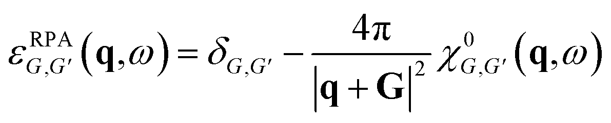
 and E0 > 0, as shown in Fig. 1. Assuming that the electron wavefunctions of the two bands are orthogonal (e.g. they arise from pz and pxy orbitals, respectively), the inter-band transition of electrons is prohibited.
 and
and  ,
,  (see Sec. S3 of the ESI for more details†). The plasmon modes are isotropic and satisfies ω ∝ q1/2 in the long-wavelength limit, similar to that of 2D electron gas.28

 and
and 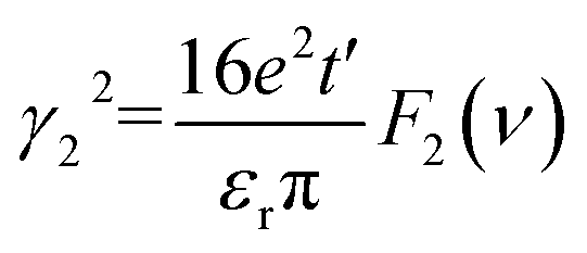 . Here, γ1 and γ2 represent the contributions of Ek,1 and Ek,2, respectively. The variation of γ1 and γ2 as a function of Fermi energy is plotted in Fig. 3(d). As Ef increases from the bottom of the band Ek,2 to the top of the band Ek,1, γ1 gradually decreases and finally becomes zero when Ef reaches the top of the band Ek,1, while γ2 shows an opposite trend. As a result, γ becomes insensitive to the Fermi energy (or carrier density).
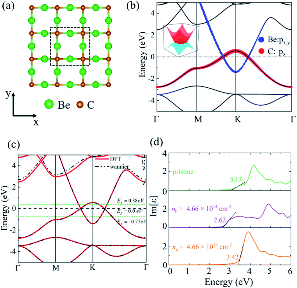
 behavior of 2D electron gas.49 But for large momentum transfer q, it deviates gradually from the
  rule. We ascribed it to the origins of the plasmons in the Be2C monolayer. In the small momentum region, the plasmons are mainly dominated by the intra-band transition of the two DNL bands. With the increase of momentum, however, the inter-band transition comes to occur and contributes to the polarization function. The consequent screening effect results in the redshift of the plasmon energy and deviation from the TB model.22 From the plasmon spectra under these three different doping conditions in Fig. 5(a), we can see that γ is nearly insensitive to the Fermi level. For further verification, we fitted the plasmon spectra of the Be2C monolayers in the low energy region by eqn (16) and got γ = 5.63 Å1/2 and 5.74 eV Å1/2 for the hole- and electron-doped Be2C monolayers with a concentration of 4.66 × 1014 cm−2, respectively, which are very close to that of the pristine Be2C monolayer, 5.76 eV Å1/2, in good agreement with the TB model.
 dispersion (solid black lines) are also shown for comparison. The shaded areas indicate the SPE regions due to inter-band (yellow) and intra-band (green) transitions, respectively.