
 Open Access Article
 This Open Access Article is licensed under a Creative Commons Attribution-Non Commercial 3.0 Unported Licence
Optimization of electron beam-deposited silver nanoparticles on zinc oxide for maximally surface enhanced Raman spectroscopy†
Andrew L.
Cook
 a,
Christopher P.
Haycook
a,
Andrea K.
Locke
a,
Richard R.
Mu
b and
Todd D.
Giorgio
*a
a,
Christopher P.
Haycook
a,
Andrea K.
Locke
a,
Richard R.
Mu
b and
Todd D.
Giorgio
*a
aDepartment of Biomedical Engineering, Vanderbilt University, Nashville, TN 37235, USA. E-mail: todd.d.giorgio@vanderbilt.edu
bTSU Interdisciplinary Graduate Engineering Research (TIGER) Institute, Tennessee State University, Nashville, TN 37209, USA
First published on 7th December 2020
Abstract
Surface enhanced Raman spectroscopy enables robust, rapid analysis on highly dilute samples. To be useful, the technique needs sensing substrates that will enhance intrinsically weak Raman signals of trace analytes. In particular, three-dimensional substrates such as zinc oxide nanowires decorated with electron-beam deposited silver nanoparticles are easily fabricated and serve the dual need of structural stability and detection sensitivity. However, little has been done to optimize electron beam-deposited silver nanoparticles for maximal surface enhancement in the unique dielectric environment of the zinc oxide substrate. Herein, fabrication and anneal parameters of electron beam-deposited silver nanoparticles were examined for the purpose of maximizing surface enhancement. Specifically, this work explored the effect of changing film thickness, deposition rate, anneal temperature, and anneal time on the surface plasmon resonance of Ag nanoparticles. In this study, multiple sets of fabrication and annealing parameters were discovered that optimized surface plasmon resonance for maximal enhancement to Raman signals acquired with a 532 nm laser. This work represents the first characterization of the fabrication and annealing parameters for electron beam-deposited silver nanoparticles on zinc oxide.
Introduction
There is an unmet multidisciplinary need for bioanalytical techniques that can perform analyses on small volumes of highly diluted specimens with minimum sample preparation. Applications such as the detection of toxic metals,1–4 other pollutants or contaminants,5–8 circulating tumor cells,9 bacteria,10 or viruses11 benefit from fast and reliable molecular sensing. State-of-the-art tools used for these purposes such as high-performance liquid chromatography, mass spectrometry, and enzyme-linked immunosorbent assays commonly involve expensive reagents, large sample volumes, skilled technicians and frequently have low throughput rates. In addition, such tools are often plagued by limited differentiation among chemically or biologically similar analytes.12–14 Raman spectroscopy is an attractive technique that addresses some of the limitations of other approaches because it provides a unique spectroscopic “fingerprint” of the biomolecular and biochemical composition of specimens, potentially offering effective detection of analytes in minutes or seconds.15–17 Raman also exhibits portability and facile function, as demonstrated by its use in forensic fields such as explosives identification.18 However, Raman scattering has a small optical cross-section, with only one in 106 to 108 photons being Raman scattered, limiting its usefulness for trace analyte sensing. Surface-enhanced Raman spectroscopy (SERS), however, can significantly enhance intrinsically weak Raman signals, enabling reliable, efficient, and non-destructive detection of highly dilute analytes.It is well-known that there are two mechanisms principally responsible for the enhancement effects in SERS: an electromagnetic mechanism resulting from localized surface plasmon resonance (LSPR) and a chemical mechanism resulting from charge transfer between analyte and metallic nanostructure.19–21 To take full advantage of the dominant electromagnetic mechanism of surface enhancement, it is necessary that the nanoparticles be spatially dense, to make use of “hotspots” in the gaps between nanoparticles.22,23 For these reasons, much attention has been devoted to the use of metallic nanoparticles for incorporating SERS into various sensing system solutions. However, the expansive parameter space controlling SERS performance requires further investigation to effectively design sensors that provide optimal surface enhancement of intrinsically weak Raman signals.
Silver (Ag) is among the most commonly used metals for SERS-based sensing, due to strong Ag plasmon resonance in the visible region24,25 and facile synthesis.26 Many Ag nanostructures have been explored for SERS-based sensing, which fall into two basic categories: (1) colloidal nanostructures and (2) nanostructures on solid surfaces.27 Colloidal nanostructures offer high sensitivity due to the ability to easily generate a large sensing surface area. However, due to random suspension of particles in free solution, colloidal nanostructures lack stability, and thus can affect measurement reproducibity. Conversely, nanostructures fabricated onto solid surfaces can possess great structural stability, resulting in greater measurement reliability. However, this stability comes at the cost of reduced sensitivity compared to colloidal paradigms due to lower surface area. This cost can be mitigated by fabricating inherently three-dimensional (3D) sensing substrates, as described in our previous work.28 There are several methods of fabricating metallic nanoparticles onto a solid substrate that generally fall into two categories: chemical fabrication and physical deposition. Physical deposition techniques such as electron beam (e-beam) deposition facilitate formation of densely arranged Ag nanoparticles, enabling use of “hot-spots” between nanoparticles.29 However, these techniques do not easily lend themselves to control of nanoparticle properties that affect LSPR. In the case of chemical fabrication, techniques such as hydrothermal growth are used to fabricate nanoparticles directly on the sensing surface.30 While these techniques are more easily implemented and easier to control than physical deposition, they usually result in lower surface coverage by nanoparticles, reducing the impact of inter-particle hotspots. Therefore, by exploring the fabrication parameters that affect nanoparticle formation in physical deposition paradigms, greater control over nanoparticle formation can be implemented.
Recent research has illuminated multiple strategies for realizing 3D templates for SERS-active substrates, including anodized aluminum oxide,31 porous silicon,32 electrospun polymers,33 silicon nanowires,34 and zinc oxide (ZnO) nanowires,30 among others. ZnO, in particular, is an attractive material for fabricating 3D SERS substrates. ZnO is a biocompatible35 wide direct-bandgap semiconductor with a band-edge emission of 3.3 eV and a high exciton binding energy of 60 meV, making it electronically stable at room temperature.36,37 The semiconducting nature of ZnO also enables charge transfer between the ZnO and Ag,38 increasing surface enhancement over strategies that rely solely on the electromagnetic mechanism. Crystalline ZnO is also transparent to visible light,39 which reduces absorptive loss of light when acquiring spectra through the substrate as we did in our previous work.28 Additionally, ZnO possesses a large refractive index of approximately 2.0 in the visible region, which aids in the confinement of light.40,41 Combining these characteristics with the atomically smooth and highly faceted hexagonal single-crystal structure of the nanowires allows for wave-guiding of light, which can reduce signal loss due to light scattered away from the detector.42
Previously, we prepared ZnO nanowires decorated with Ag nanoparticles for sensing soluble analytes. This sensing paradigm yielded an estimated six orders of magnitude surface enhancement of the Raman signal for crystal violet (CV, CCDC # 137090), melamine, and adenine.28 Performance of this sensor was likely reduced because the Ag nanoparticles, with a plasmon peak at ∼460 nm, were not optimal for SERS with the 532 nm laser used. We also did not explore the sensor performance as a function of Ag deposition parameters that are likely to influence SERS amplification mechanisms. Through this study, Ag-decorated ZnO nanowires demonstrated potential for effective sensing of trace analytes, which can be realized by examining the effect of fabrication and anneal parameters on surface plasmon resonance.
Parameters that can be manipulated during e-beam deposition of Ag and significantly impact the Raman enhancement include film thickness and deposition rate. Film thickness, in general, changes the shape and surface coverage of metallic nanostructures which changes LSPR characteristics of the film. By consequence, these changes modulate the magnitude of surface enhancement. Other research groups have explored how Ag nanoparticle plasmon resonance changes with film thickness in e-beam deposited43 and sputtered44 systems, but in neither of these works were nanoparticles deposited on a ZnO layer, which can significantly impact plasmon resonance as part of the dielectric environment of the nanoparticles. Also, while the effects of Ag film thickness on LSPR has been explored in some way, little attention has been devoted to the effects of Ag film deposition rate on plasmon resonance, even though deposition rate has a known effect on the structural properties of metallic films.45 Furthermore, thermal annealing following deposition changes the nanoparticle size and shape through Ostwald ripening.46 Since nanoparticle geometry and dimensions are important drivers of plasmon resonance, thermal annealing offers an additional strategy for optimization of SERS sensing. Thermal annealing occurs as a result of two independent parameters: anneal temperature and anneal time.
In this work, four independently selectable parameters that influence Ag nanoparticle formation and presentation on ZnO were quantitatively controlled. These parameters, namely film thickness, deposition rate, anneal temperature, and anneal time were examined to assess their impact in modulating surface plasmon resonance. The functional consequences of these fabrication parameters were comparatively assessed using surface-enhanced Raman spectra that were acquired from crystal violet deposited onto each substrate. We aim to discover fundamental fabrication principles and sensor characteristics that will advance the design of maximally sensitive SERS devices based upon e-beam deposited Ag nanoparticles on a ZnO substrate.
Experimental
Substrate preparation
Glass slides (Fisherbrand® Plain Microscope Slides) were cut into 80 1 cm2 substrates with a diamond saw and cleaned by sonication sequentially for 10 minutes each in 1% aqueous Alconox® solution, deionized (DI) water, acetone, methanol, and again in DI water. Onto these substrates, a 100 nm ZnO layer was deposited via e-beam deposition at a rate of approximately 0.1 Å s−1 to ensure even deposition of Zn and O. As demonstrated by Fig. S1,† Masks were cut from aluminum foil large enough to completely cover the substrates, with a square cutout ∼0.2 cm to a side, allowing a Ag film to be deposited on only a small portion of each substrate. After each film was deposited, the masks were shifted so that the cutouts exposed a new portion of each substrate, and a new film was deposited. This process was repeated nine times, for nine different Ag film thicknesses fit on each substrate, as illustrated by Fig. S1.† Ag thin films were deposited over a range of 1 nm to 9 nm film thicknesses, in 1 nm increments, hereafter referred to as T1–T9. The 62 substrates were divided into two groups of 31 substrates, as shown in Fig. 1. In each group, 30 substrates would be annealed and 1 would remain unannealed. These two groups, hereafter referred to as group A and group B, were deposited with Ag thin films at rates of 0.1 and 0.3 Å s−1, respectively. All Ag films in group A were deposited at rates of 0.1 ± 0.002 Å s−1 and all Ag films in group B were deposited at rates of 0.3 ± 0.018 Å s−1. It is well known that when material from a point source is deposited onto substrates affixed to a flat plate, deposition rates fall off with axial distance from the source. This results in varying film thickness as a function of axial distance, defined by eqn (1):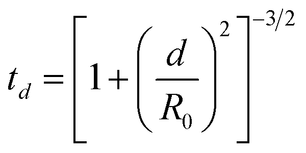 | (1) |
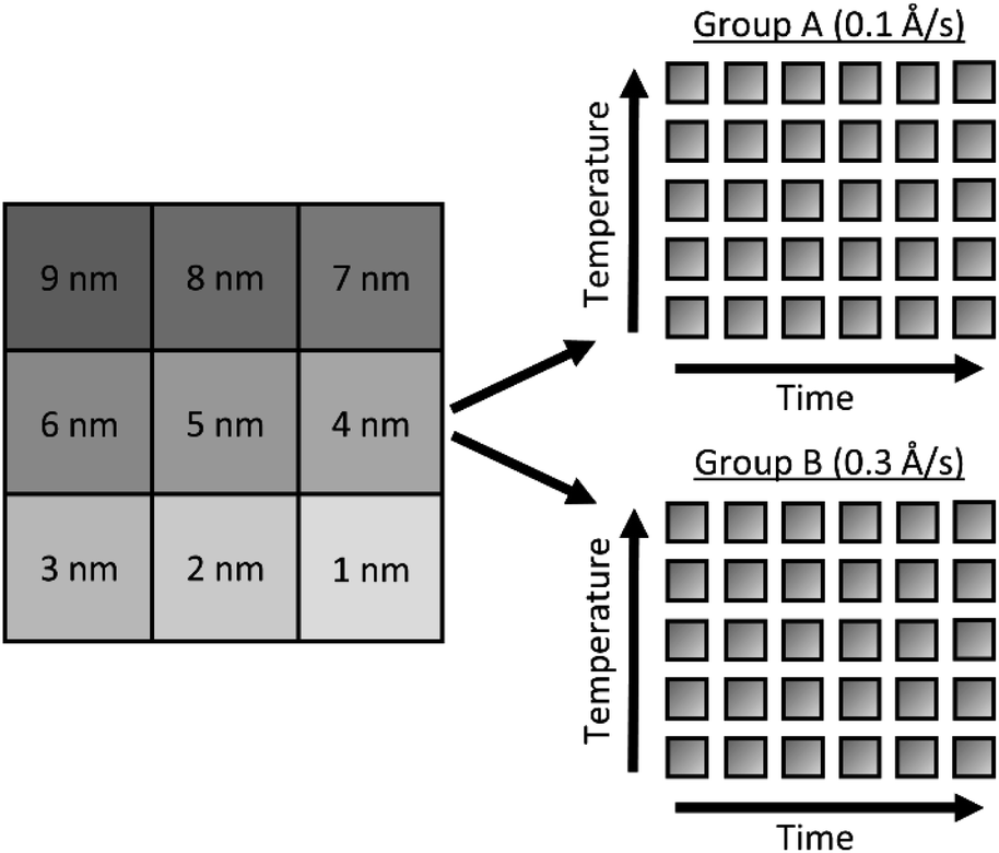 | ||
| Fig. 1 Schematic of substrates used for parameter exploration. Substrates deposited with 9 different Ag film thicknesses and separated into two rate groups (A and B). In each group, substrates are annealed over a range of times (15–150 min) and temperatures (50–400 °C). | ||
In this equation, td represents the film thickness at distance d from the axis defined by the point source and R0 represents the distance from the source to the plane of deposition. R0 was measured to be 27 cm and the axial distance d of substrates farthest from the source was measured to be ∼4.5 cm. Thus, the largest variation in film thickness was ∼4% of the target thickness. All e-beam depositions were performed at pressures below 6.7 mPa.
Following the deposition of silver, the substrates were annealed at various temperatures: 50, 100, 200, 300 and 400 °C. At each temperature, different substrates were annealed at times: 15, 30, 60, 90, 120, and 150 minutes, providing a substrate from each deposition rate group (2 groups) with every anneal temperature (5) and time (6), producing 2 × 5 × 6 = 60 uniquely fabricated and annealed substrates and 1 unannealed control per group, each presenting T1 through T9 film thicknesses for a total of 558 different substrates.
Optical characterization techniques
Scanning electron microscopy (SEM) images, before annealing, were acquired of each Ag film thickness from a random substrate to get a visual perspective on the changing Ag nanostructure morphology as a result of changing film thickness. These images were acquired using a Zeiss Merlin scanning electron microscope (Jena, Germany) in a plan configuration with a 10 kV electron beam at a magnification of 400![[thin space (1/6-em)]](https://www.rsc.org/images/entities/char_2009.gif) 000× and a working distance of 2.8 mm. The average size of nanostructures was determined using Fiji image analysis of acquired SEM images.47,48 The images were first converted to black-and-white via the Make Binary function and noise was removed via the Despeckle function, in which each pixel is given the median value of its 3 × 3 neighborhood. The area of the nanostructures were acquired via the Analyze Particles function and area values that didn't correspond to single nanostructures were removed.
000× and a working distance of 2.8 mm. The average size of nanostructures was determined using Fiji image analysis of acquired SEM images.47,48 The images were first converted to black-and-white via the Make Binary function and noise was removed via the Despeckle function, in which each pixel is given the median value of its 3 × 3 neighborhood. The area of the nanostructures were acquired via the Analyze Particles function and area values that didn't correspond to single nanostructures were removed.
Extinction spectra were acquired of each film thickness, on each substrate before and after annealing, using a Hitachi U-4100 spectrophotometer integrating sphere to determine peak surface plasmon resonance wavelength. Extinction spectra were obtained at a rate of 3 nm s−1 over a range of 350–850 nm, with each substrate oriented facing away from oncoming light.
Raman spectra were acquired using a Thermo Scientific DXR Raman microscope (Waltham, MA, USA). A 532 nm diode-pumped, solid state (DPSS) laser was used with a 10× objective (Olympus, MPlan N Achromat, 0.25 NA) at a power of 10 mW as measured at the objective turret. Focal plane was adjusted before each acquisition to maximize spectral intensity. All substrates were placed in contact with a 25 μM aqueous solution of crystal violet (CV) overnight. The substrates were then removed from the CV solution and air-dried. Five Raman spectra were acquired from each substrate (T1–T9), along with five spectra of a portion on each substrate without Ag, hereafter referred to as T0. Each Raman spectrum was the accumulation of four background-subtracted spectra acquired over a range of 200–1800 cm−1, each taken with a 5 s exposure time. All Raman spectra were acquired with a 50 μm pinhole aperture and a 900 grooves per mm grating.
Spectral processing
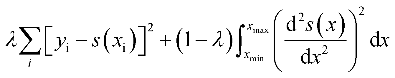
UV-Vis spectra of the Ag films deposited on ZnO layers exhibit extinction from both Ag and ZnO. While ZnO is largely transparent in the visible region, light extinction due to the ZnO band edge occurs below approximately 380 nm. In order to accurately obtain Ag plasmon peak information, absorptive contributions from ZnO were approximated and subtracted as illustrated in Fig. S2.† This method was chosen to minimize variation in ZnO signal induced by the fabrication and anneal process, as illustrated by Fig. S3.† To approximate ZnO absorptive contributions, UV-Vis spectra from the T1 portions of each substrate were fitted to a tri-gaussian equation, shown in eqn (2). In this fit, the first gaussian approximated the ZnO band-edge contribution, the second approximated the ZnO visible contribution, and the third approximated the Ag plasmon peak. T1 spectra were chosen for this task because of minimal overlap between the Ag plasmon peak and the ZnO band-edge and because the plasmon peak could be accurately approximated by a gaussian curve. Once fits to these spectra were successfully obtained, the third gaussian was subtracted from the fit to arrive at an approximation of the ZnO contribution to the spectra. This ZnO contribution for each substrate was then subtracted from the UV-Vis spectra for T1–T9 for each substrate. Finally, a cubic smoothing spline, where eqn (3) is minimized, was fit to the resultant plasmon peaks to remove noise, enabling accurate extraction of plasmon peak extinction, wavelength, and spread.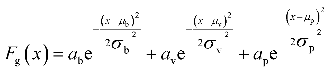 | (2) |
 | (3) |
In eqn (2), Fg is the gaussian fit, a is an arbitrary fit parameter, and μ & σ represent the peak and root-mean-square width of the gaussian, respectively. Subscripts b, v, and p denote the gaussian fitting of the ZnO band-edge, ZnO visible, and Ag plasmon contributions to the spectrum, respectively. In eqn (3)λ represents the smoothing parameter, y is the set of observed extinctions at each wavelength, x is the set of wavelengths at which extinction is measured, s is the smoothed function output of the equation, and xmin & xmax are the minimum and maximum wavelengths of the spectrum, respectively. For this work, a smoothing parameter λ = 0.003 was used. A smoothing spline was used to approximate the plasmon rather than a gaussian because, while the plasmon peaks of thinner films could be accurately approximated by a gaussian fit, the plasmon peaks of thicker films could not due to increasing asymmetry in the peak. Spread was measured at the full width-half maximum (FWHM) of each plasmon peak where possible. For several spectra, particularly of thicker Ag, the FWHM was sufficiently broad to extend beyond the measured wavelength range and could not be determined. All processing of UV-Vis spectra was performed in MATLAB.49 Energy dispersive X-ray spectroscopy had been previously performed on similarly prepared SERS-active substrates, confirming the presence of ZnO and Ag.28 Raman spectra were subtracted of their fluorescent background, estimated using 5th-degree polynomial fit. These spectra were then smoothed using a Savitzky–Golay filter. Each of the five spectra acquired from each film thickness (T0–T9) on each substrate were averaged to find a representative spectrum. Three CV Raman peaks at 420, 915, and 1592 cm−1, tabulated in Table 1 with their associated vibrational modes and the CV molecular structure, were selected to provide specific, characteristic features for the estimation of enhancement factors (EFs). These peaks were selected to interrogate EFs from each end of the measured spectra and one feature near the middle of the spectra. The intensities of these peaks in the spectra for T1–T9 on each substrate were divided by the intensities of the same peaks in the spectrum of T0 on the same substrate to arrive at EFs for each peak.
| Raman band (cm−1) | Non-benzene vibrational modes | Benzene modes | Molecular structure |
|---|---|---|---|
| 420 | δ(C–Ccenter–C)/δ(C–N–C)‖ | 16a |
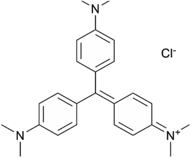
|
| 915 | δ(C–Ccenter–C) | 12,17a | |
| 1592 | 8a |
Statistical analysis
All error bars represent standard deviation unless otherwise stated. Two-way analysis of variance followed by Tukey's and Sidak's multiple comparison tests was performed for data presented here as indicated, and statistical significance was defined as p < 0.05. Statistical analyses were performed using Prism 7.04 (GraphPad Software).Results & discussion
The surface plasmon peak of a distribution of Ag nanoparticles possesses three characteristics that affect the level of enhancement: peak intensity, peak wavelength, and peak breadth. Because surface plasmons enhance both incident light from the laser and Raman-scattered light, surface enhancement is most effective when high plasmon extinction occurs at both the laser line and across the range of wavelengths at which light is scattered. Thus, the surface plasmon peak should be located near the laser line to maximize enhancement to incident light, and the peak should be sufficiently broad to provide significant enhancement to Raman-scattered light across the wavelength range of interest. In addition, plasmon intensity correlates with enhancement factor, with higher plasmon intensities generally producing greater enhancement for non-colloidal sensing substrates.50 Surface plasmon peak intensity, wavelength, and breadth are all influenced by nanoparticle size, size distribution, crystal composition, proximity, and shape. These nanoparticle properties are modulated by deposition thickness and deposition rate, and by anneal temperature and time, post-deposition. In this study, we explore the combinatorial effect of these fabrication parameters on the surface plasmon peak characteristics of Ag nanoparticle arrays and correlate these effects to changes in enhancement of intrinsic Raman spectral intensity of CV. By doing so, we aim to facilitate the development of optimized sensing substrates for maximally surface-enhanced Raman spectroscopy.Effect of film thickness on surface enhanced Raman spectroscopy
Increasing Ag film thickness was anticipated to intensify, broaden, and red-shift the plasmon extinction peak due to increasing Ag surface coverage, increasing particle diameter, and decreasing interparticle distance. However, the quantitative relationships that describe these effects as a function of film thickness have not been previously described. Furthermore, while increasing intensity is correlated with increasing surface enhancement, for solid substrates, maximizing enhancement requires proximity of the peak wavelength with the incident laser. In addition, broadening the plasmon peak is only effective insofar as it maximizes plasmon extinction across the wavelengths of interest. Therefore, we examined the relationships between Ag film thickness and maximized surface enhancement through changes to nanostructure morphology and plasmon peak extinction characteristics. SEM images were acquired from group A before annealing to explore the relationship between film thickness and nanostructure morphology. These images, shown in Fig. 2, reveal that Ag was deposited as small islands that grow with increasing film thicknesses from 1 nm (T1) to approximately 5 nm (T5) and become more film-like for depositions of 6 nm (T6) and greater. This change is likely due to surface coverage approaching 100% as a result of increasing Ag mass per area. Extinction spectra are superimposed on each SEM image in Fig. 2, confirming intensified and red-shifted extinction with increasing film thickness. The symmetrical plasmon peaks observed among the lowest Ag depositions (T1–T4) are consistent with individual, spherical Ag nanoparticles. The transition toward nanostructured thin films (T5–T9) was accompanied by increasingly exotic nanostructure shapes, associated with increasing asymmetry in the plasmon peaks.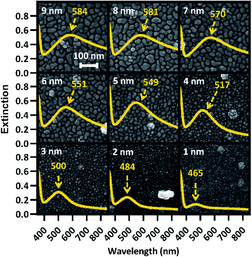 | ||
| Fig. 2 SEM images of all film thicknesses (identified in white) for a random substrate, with associated extinction spectra displaying peak plasmon wavelength overlaid. The plasmon peak wavelength is identified in yellow for each extinction spectrum. | ||
The UV-Vis spectra for all 9 film thicknesses on each of 40 substrates in group A were processed as described in the Experimental section above to find peak extinction intensity, wavelength, and breadth in each case. Plasmon extinction intensity increased with Ag film thickness, as shown in Fig. 3(a). Intensity increases approximately linearly for T1–T5, but begins to approach an asymptotic maximum for T6–T9. The reduction in differential extinction for high film thicknesses is confirmed by the lack of statistically significant differences between T7 & T8 and T8 & T9 as compared to T1–T6 in which each thickness group was significantly different from every other thickness group. This change in behavior between thin and thick films correlates with proximity-induced hotspots. When adjacent nanoparticles are within a few nanometers of each other plasmonic coupling results in a hotspot between them, greatly increasing plasmon extinction.22 For T1–T5, plasmonic coupling between nanoparticles drove the growth in plasmon extinction intensity as interparticle distances decreased, exhibited by Fig. 2. Beginning at T6 however, interparticle gaps ceased to decrease as Ag was deposited. At that point, plasmon extinction intensity began to plateau, which is consistent with Ag accumulation becoming the primary driver for increasing plasmon extinction.
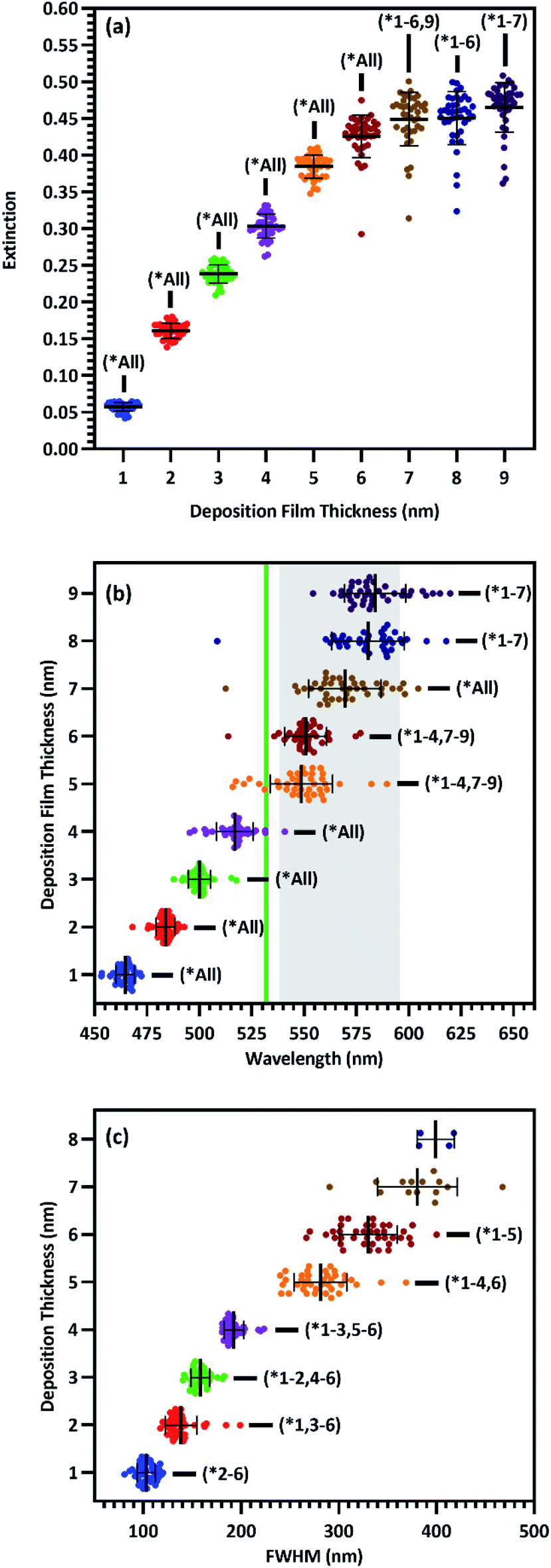 | ||
| Fig. 3 Scatterplots of plasmon peak (a) intensity (n = 40), (b) wavelength (n = 40), and (c) FWHM (T1–T4: n = 40, T5–T6: n = 39, T7: n = 14, T8: n = 4) for each film thickness of substrates in group A. Green line and shaded region in (b) represent the laser line and fingerprint region, respectively. All data shown with mean and standard deviation of each group, *p < 0.05 two-way ANOVA. Statistical significance of the FWHM of 7 and 8 nm films as compared to other films not shown due to an insufficient number of data points to use a parametric test. | ||
Plasmon peak wavelength red-shifted with increasing Ag film thickness, shown in Fig. 3(b), from well below the laser line at an average of ∼464 nm for 1 nm films, to well past the laser line at an average of ∼584 nm for 9 nm films. This redshift was likely due primarily to increasing nanostructure size, which correlated with increasing film thickness (Fig. 2). Nanostructures increased in size from an average of ∼30 nm2 for 1 nm films to an average of ∼970 nm2 for 9 nm films, as shown in Fig. S4.† Unlike intensity, maximizing surface enhancements requires proximity of the plasmon extinction peak and the laser wavelength, illustrated by the green line in Fig. 3(b). The wavelength of peak plasmon extinction also influences surface enhancement, as the efficiency of optical coupling is enhanced when the laser line is near the plasmon peak. The closest alignment between peak extinction and the laser line was at 517 nm for T4 and 548 nm for T5. Additionally, variability in peak wavelength generally increased as films thickened, with standard deviation growing from 4.2 nm for 1 nm films to as much as 17.3 nm for 8 nm films. We speculate that this behavior is associated with the increasingly exotic nanostructure shapes associated with increasing film thickness.
Maximal surface enhancement requires LSPR with both incident laser light and wave-shifted scattered light. While enhancement is improved when the plasmon extinction peak is close to the laser wavelength, the peak should also be sufficiently broad to enhance wave-shifted scattered light across the fingerprint region which, for organic molecules, usually consists of some portion of the region between 200 and 2000 cm−1. When a 532 nm laser is used to acquire Raman spectra, this fingerprint region translates to 537.7–595.3 nm, illustrated by the shaded region in Fig. 3(b).51–54 Thus, the sensing approach aims for a plasmon wavelength range that usefully overlaps with the entire spectral region of interest. To estimate breadth of the plasmon peak, the FWHM was determined where possible. FWHM of the plasmon peaks correlate with film thickness and range from ∼104 nm for 1 nm films to more than 400 nm for 8 nm films, as shown in Fig. 3(c). While this phenomenon provides a greater wavelength range with the potential for useful sensing at the largest deposition thicknesses, it complicated our ability to accurately characterize the FWHM. For substrates with T5 and T6 film thickness, a FWHM could be calculated for 39/40 spectrums. For T7, a FWHM could only be calculated for 14/40 spectra. For T8, a FWHM could only be calculated for 4/40 spectra, and for T9, no FWHM's could be calculated. This phenomenon correlated with the increasing asymmetry of the plasmon peaks as films transitioned from individual nanoparticles to nanostructured films, shown in Fig. 2. This increasing asymmetry was beneficial for maximizing surface enhancement due to greater plasmon resonance across the fingerprint region.
Analyses of individual plasmon characteristics indicated that the film thickness required to produce maximal surface enhancement would optimize the balance among plasmon extinction intensity, peak proximity to the laser line, and extinction intensity across the fingerprint region. Because these plasmon extinction characteristics interact in non-obvious ways to influence the overall Raman spectra enhancement, SERS spectra of CV adsorbed onto the Ag films were acquired and shown in Fig. 4(a) to characterize the role of film thickness on surface enhancement. CV possesses multiple strong Raman peaks, tabulated in Table S1† with their associated vibrational modes, across a large portion of the fingerprint region,55 Very little enhancement was observed for T1–T4, with the T4 film resulting in less than 5-fold enhancement across the fingerprint region as compared to the T0 spectrum. This inconsequential enhancement likely resulted from a combination of low plasmon intensity (Fig. 3(a)), inefficient coupling between the plasmon peak and the laser line (Fig. 3(b)), and insufficient peak breadth to enhance wave-shifted light across the fingerprint region. However, enhancement notably increased starting at T5, with up to 15.8-fold enhancement as compared to the T0 spectrum at 1592 cm−1. Maximal enhancement was found to occur for the T7 film, with up to 25.7-fold enhancement across the fingerprint region at 1592 cm−1, before decreasing with T8 and T9 films. The diminished enhancement for the thickest Ag films is correlated with an increasing departure from the laser line due to red-shifting peak plasmon extinction (Fig. 3(b)) accompanied by decreasing rate of plasmon extinction intensification (Fig. 3(a)). These results are non-obvious when assessing plasmon peak characteristics individually, illustrating the value in analyzing relationships between these characteristics in light of how they influence surface enhancement. These results demonstrate that film thicknesses of 5 nm or greater provide the best surface enhancement, peaking with 7 nm film thickness. Thus, continued analysis focused on thicker films of 5 nm and above.
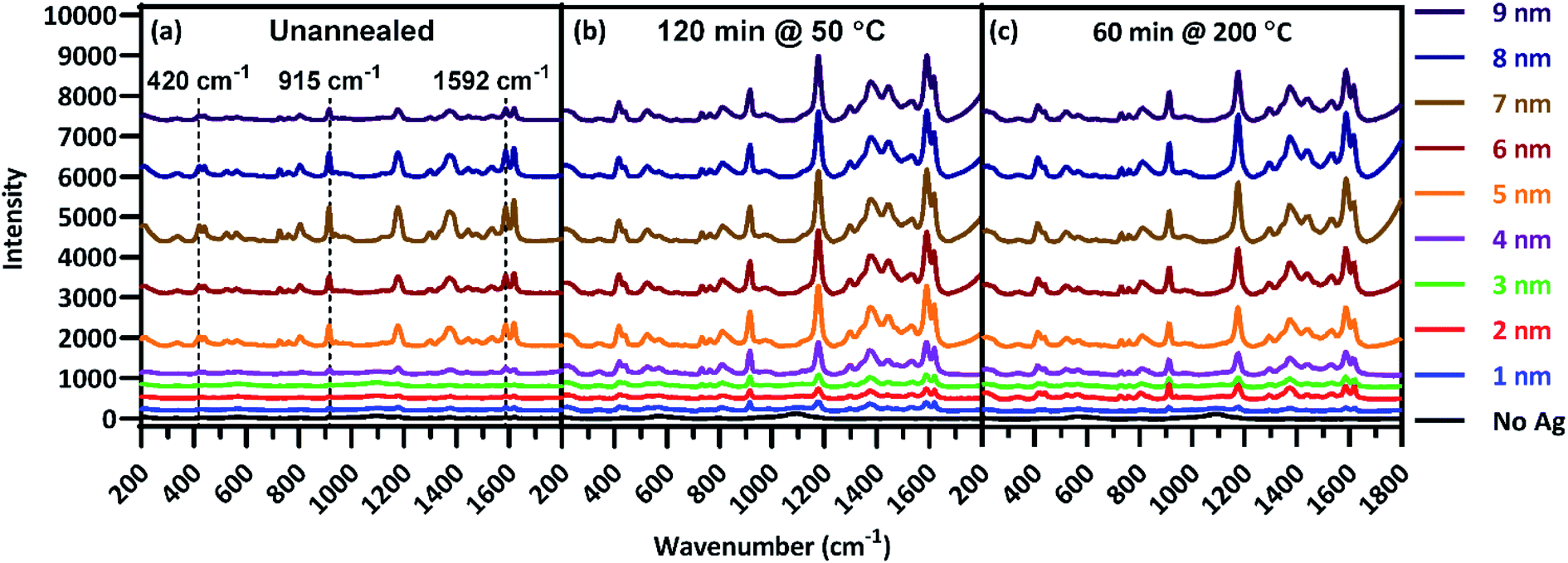 | ||
| Fig. 4 Raman spectra of CV deposited on each film thickness for substrates (a) unannealed, (b) annealed at 50 °C for 60 min, and (c) annealed at 200 °C for 60 min. | ||
Effect of annealing on surface enhanced Raman spectroscopy
Following the analysis of deposition thickness, substrates were annealed to explore the effect of annealing temperature and time on plasmon extinction characteristics, toward additionally maximizing surface enhancement. From group A, 31 substrates from group A were chosen for this analysis, with the remaining 9 held in reserve should they be needed. Of the 31 substrates, one was set aside as an unannealed control and the remaining 30 were annealed at five temperatures in the range of 50–400 °C for six anneal times in the range of 15–150 min. Raman spectra were acquired of CV adsorbed onto Ag films after annealing, examples of which are presented in Fig. 4(b and c). As with the pre-anneal spectra in Fig. 4(a), film thicknesses of 5–9 nm provided the best surface enhancement for both annealed substrates presented in Fig. 4(b and c), peaking at 7 nm. However, the difference in surface enhancement between 7 nm and 5 or 9 nm films is much less pronounced for the annealed substrates than the unannealed substrate. Thus, annealing can be used to obtain near-maximum surface enhancement over a range of film thicknesses. Such flexibility in deposition thickness may be especially useful for three-dimensional sensing substrates such as ZnO nanowires. In such cases, thicker films may over-fill interwire gaps, reducing effective surface area. Because maximal surface enhancement results in part from enhancement of Raman-scattered light across the fingerprint region, three CV peaks at 420, 915, and 1592 cm−1 as identified in Fig. 4(a) were chosen to quantitatively assess enhancement at multiple points that span the fingerprint region. The enhancement of these peaks was calculated for T5–T9 at each anneal temperature and time. These enhancements appear as a heat map in Fig. 5, where red shading indicates increased enhancement. Annealing produced substantial impact to surface enhancement, but in ways that are nonlinear with respect to time and temperature. Annealing conditions generated changes to surface enhancements ranging from less than 3% to almost 3000% of the unannealed surface enhancement. Clearly, the selection of annealing parameters measurably impacts the performance of these sensors. Fig. 5 reveals that annealing at 400 °C for even a short time drastically reduced surface enhancement across the board, indicating an upper temperature limit for this sensing paradigm well below 400 °C. Further examination of Fig. 5 reveals that in general, the anneal time required to maximize surface enhancement decreased as anneal temperature increased. At 50 °C, maximizing enhancement required 120 min while at 100 °C, enhancement dropped off significantly after annealing 90 min. At 200 °C, enhancement was strongest when annealed from 15–60 min. Two of these anneal temperatures, 50 °C and 200 °C, produced particularly strong results toward maximizing surface enhancement, motivating closer examination.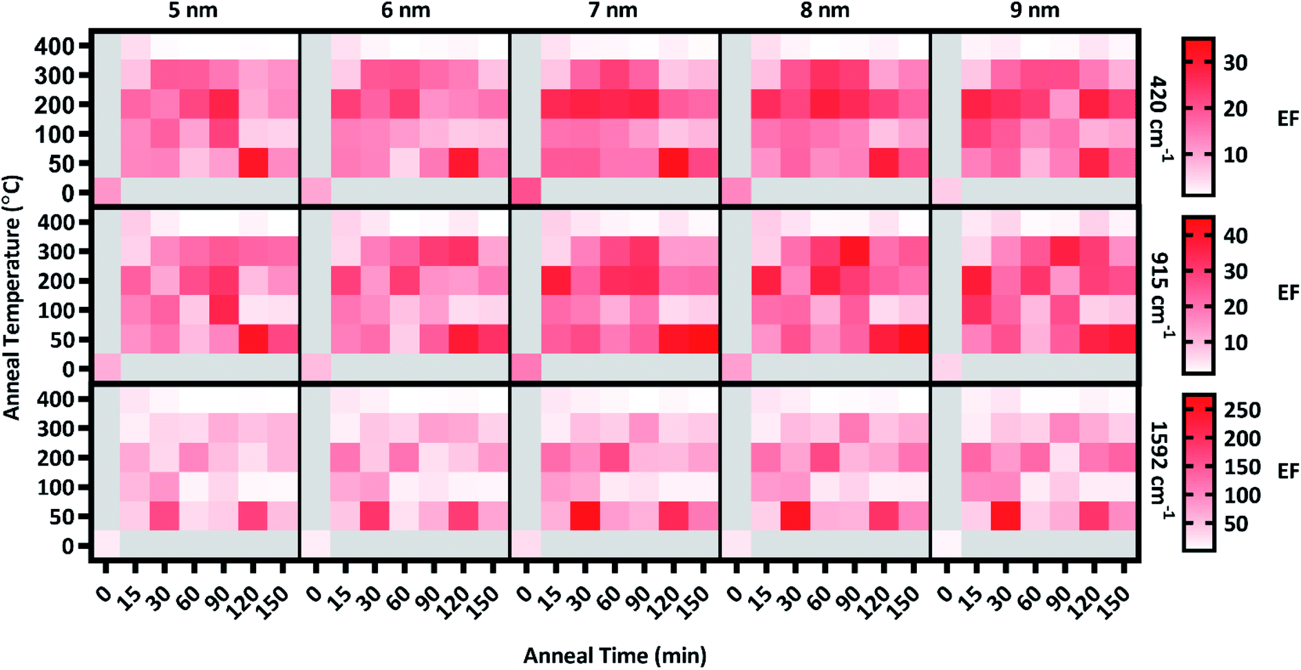 | ||
| Fig. 5 Heat map of the enhancement factors of T5–T9 for 420, 915, & 1592 cm−1 peaks across all anneal temperatures & times along with the unannealed control. | ||
Enhancement factors for the five film thicknesses were averaged for each anneal time at each temperature and plotted in Fig. 6. The relative strength of enhancement between the two anneal temperatures varies across the three CV peaks, indicating the necessity of investigating enhancement across the entire fingerprint region. For instance, annealing at 30 °C resulted in opposing enhancement trends for the two anneal temperatures. Relative enhancement decreased farther away from the laser wavelength when annealed at 200 °C while it increased away from the laser wavelength when annealed at 50 °C. Among this variability, two anneal times produced consistently strong surface enhancement at these temperatures: 60 min at 200 °C and 120 min at 50 °C.
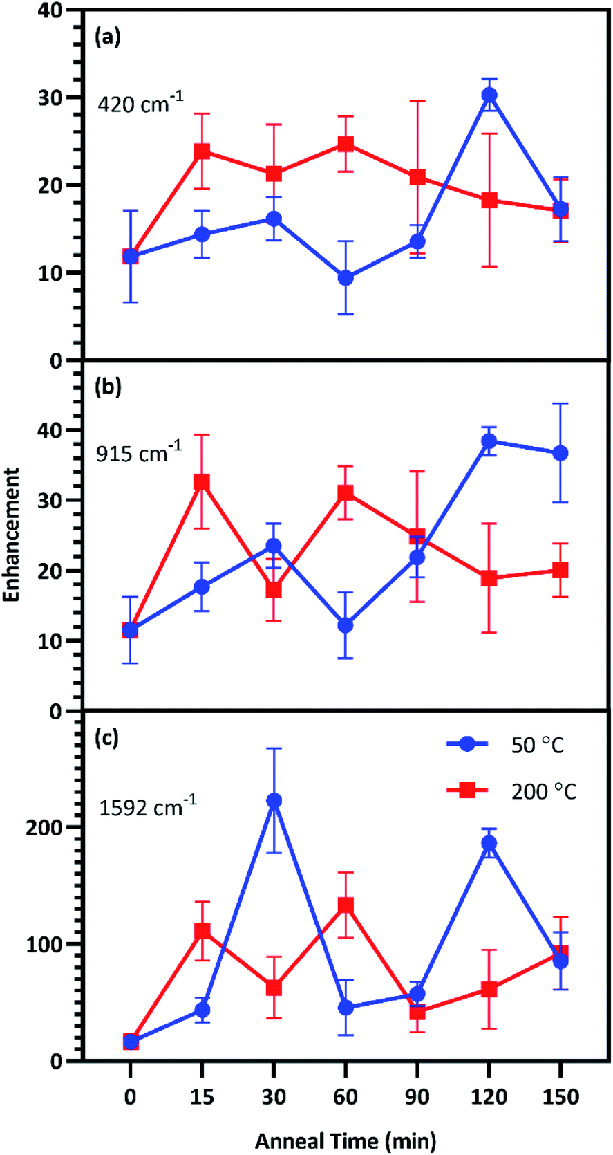 | ||
| Fig. 6 SERS EFs of substrates annealed at 50 °C (blue) and 200 °C (red) for up to 150 min, along with the unannealed control for the (a) 420 cm−1, (b) 915 cm−1, and (c) 1592 cm−1 peaks. Each point in the figure exhibits the mean and standard deviation of the EFs for T5–T9. | ||
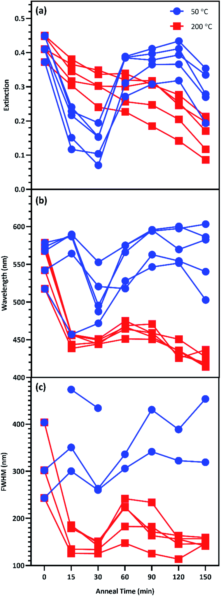
This study seeks to not only describe the deposition and annealing parameters that result in maximal surface enhancement, but also relate these results to changes in plasmon extinction characteristics effected by those fabrication parameters. To this end, changes to plasmon extinction characteristics for all five effective film thicknesses (T5–T9) due to annealing at 50 and 200 °C were plotted in Fig. 7. Annealing at 200 °C caused the plasmon intensity of all five film thicknesses to decrease steadily with increasing anneal time. In addition, annealing for 15 min or more at 200 °C blue-shifted the plasmon peaks. Annealing for 60 min slightly red-shifted the peaks, which blue-shifted again at higher anneal times (>90 min). This blue-shifting behavior is consistent with increasing nanostructure uniformity due to Ostwald ripening, reducing the exotic nature of nanostructure shapes. FWHMs followed a similar behavior as peak wavelengths, with a short anneal time narrowing the plasmon peaks. These plasmon peaks widened slightly when annealed for 60 min before narrowing again beyond 90 min. These observations agree with the results in Fig. 6, indicating that annealing at 200 °C generated the best combination of plasmon intensity, peak wavelength, and peak width at 60 min of anneal time.
 | ||
| Fig. 7 Change to the plasmon peak (a) intensity, (b) wavelength, and (c) FWHM due to anneal time at 50 °C (blue) and 200 °C (red) for T5T9. | ||
Annealing at 50 °C for less than 60 min reduced peak intensity that rebounded for anneal times of 60–120 min. Peak wavelength blue-shifted slightly following annealing for less than 60 min at 50 °C before subsequent red-shifting for annealing times of 60–120 min. FWHMs for 5 and 6 nm films were increased with increasing anneal time. These results agree with the results in Fig. 6 that indicate an optimum anneal time of 120 min at 50 °C. We anticipate that deposition and dewetting kinetics differ between the ZnO films used in this work and ZnO nanowires often utilized in 3D SERS substrates. However, this work expedites future nanoparticle optimization by narrowing the window of parameters values to explore in future works involving ZnO nanowires.
Effect of deposition rate on surface enhanced Raman spectroscopy
Deposition rate had a significant impact on plasmon peak wavelengths, with films deposited at 0.3 Å s−1 exhibiting significantly red-shifted peaks compared to a deposition rate of 0.1 Å s−1 for each film thickness examined, excepting 7 nm, as shown in Fig. S5(b).† We hypothesize that this behavior can be explained by rate-induced differences in the crystal structure of Ag nanoparticles, as deposition rate has been shown to effect such crystal properties as grain size, dislocation density, and twin boundary density in metallic nanostructures.45 These results suggest that the plasmon characteristics of e-beam deposited Ag films are sensitive to deposition rates, as small changes can have a significant impact on important physical characteristics of the nanoparticles. These results also clearly indicate the trade-off between degraded sensor performance and the reduced deposition time achieved at elevated deposition rate.While there was no significant difference in terms of enhancement in the unannealed controls between groups A (0.1 Å s−1) and B (0.3 Å s−1), Fig. S6† demonstrates that annealing the substrates in group A generally produced more surface enhancement than group B, across all film thicknesses, and anneal temperatures/times. This suggests that rate-induced differences in the crystal structure of Ag nanoparticles impacts annealing-induced effects on surface enhancement. This observation further emphasizes the important impact of deposition rate on the physical characteristics of Ag nanoparticles and the resulting surface enhancement of the structure.
Several combinations of fabrication and anneal parameters maximize surface enhancement by optimizing plasmon extinction. This study substantially improves the potential for fabricating high-performance sensors through elimination of fabrication parameters that yield low-enhancement materials. Importantly, these results demonstrate that maximal surface enhancement can be achieved by multiple different fabrication strategies. For instance, 2D sensing surfaces where film thickness does not impact device function have the best enhancement with a 7 nm thick surface deposited at 0.1 Å s−1 and annealed at 200 °C for 60 min. However, for 3D sensing surfaces such as the ZnO nanowire-based structure described in our previous work,28 a thicker sensing surface could reduce device functionality by over-filling the spaces between nanowires, thereby reducing effective surface area. In such cases, a film approximately 5 nm thick, deposited at 0.1 Å s−1 and annealed at 200 °C for an hour is predicted to provide near-maximal surface enhancement without sacrificing sensing surface area. Another consideration is the substrate on which such nanostructures are fabricated. Many sensing strategies utilize substrates with high melting points such as glass or fused silica. In such cases, annealing at 200 °C is not problematic. However, increasing attention has been devoted in recent years toward fabricating SERS-active structures on flexible substrates made of materials like polyvinyl alcohol (PVA),56,57 poly(dimethylsiloxane) (PDMS),58 or polyvinylidene fluoride (PVDF).59 In such cases substrates, even temperatures as low as 100 °C can have an undesirable effect on the substrate itself, such as increasing brittleness. For such device designs, excellent surface enhancement can be achieved by annealing substrates at 50 °C for 120 min.
Conclusions
This study provides guidance for the fabrication of sensors with maximal SERS enhancement excited with a 532 nm laser through e-beam deposited Ag nanoparticles on ZnO. 7 nm Ag films possess the optimal combination of plasmon peak intensity, wavelength, and breadth for maximal surface enhancement with a 532 nm laser. When 7 nm films are untenable, films as thin as 5 nm still provide near-maximal surface enhancement. We demonstrated that annealing at temperatures up to 200 °C for one to two hours further improved surface enhancement, but annealing at 200 °C for one hour or 50 °C for two hours resulted in the greatest increase to surface enhancement. Lastly, we discovered that Ag deposition rate significantly influences surface plasmon extinction peak characteristics. Increasing deposition rate from 0.1 to 0.3 Å s−1 resulted in decreased surface enhancement at all anneal times and temperatures, making 0.1 Å s−1 the clearly preferable deposition rate. The results presented in this study fill a vital need for guidance in determining fabrication and annealing parameters for maximal SERS with e-beam deposited Ag nanoparticles with a 532 nm laser. We presume that similar fabrication relationships control the performance of other SERS substrates based on metal nanoparticles. This is the first report to begin to explore the impact of fabrication choices on the performance of a specific SERS sensor, but lays the groundwork for the assessment of similar phenomena in other Raman sensing approaches.Conflicts of interest
There are no conflicts of interest to declare.Acknowledgements
A. L. Cook acknowledges support from the National Science Foundation Graduate Research Fellowship Program (NSF GRFP) 1445197. A. L. Cook and T. D. Giorgio also acknowledge support from the Congressionally Directed Medical Research Program (CDMRP) Peer Reviewed Medical Research Program (PRMRP) W81XWH-18-1-0412. C. P. Haycook acknowledges support from the National Heart Lung and Blood Institute (NHLBI) T32HL144446. R. R. Mu acknowledges support from the NSF Historically Black Colleges and Universities Research Infrastructure for Science and Engineering (HBCU-RISE) 1924241. The authors would like to thank Eugene Collins, PhD and Akira Ueda, PhD at Fisk University for the use of their facilities and equipment. Lastly, the authors would like to thank Dmitry Koktysh, PhD for his assistance and the Vanderbilt Institute of Nanoscale Science and Engineering (VINSE) for the use of their facilities and equipment in the course of this study.References
- D. K. Sarfo, A. Sivanesan, E. L. Izake and G. A. Ayoko, RSC Adv., 2017, 7, 21567–21575 RSC.
- S. Jayabal, A. Pandikumar, H. N. Lim, R. Ramaraj, T. Sun and N. M. Huang, Analyst, 2015, 140, 2540–2555 RSC.
- M. S. Frost, M. J. Dempsey and D. E. Whitehead, Sens. Actuators, B, 2015, 221, 1003–1008 CrossRef CAS.
- Y. Zeng, J. Ren, A. Shen and J. Hu, ACS Appl. Mater. Interfaces, 2016, 8, 27772–27778 CrossRef CAS.
- C. Rosman, J. Prasad, A. Neiser, A. Henkel, J. Edgar and C. Sönnichsen, Nano Lett., 2013, 13, 3243–3247 CrossRef CAS.
- R. A. Halvorson and P. J. Vikesland, Environ. Sci. Technol., 2010, 44, 7749–7755 CrossRef CAS.
- W. F. Pearman, S. M. Angel, J. L. Ferry and S. Hall, Appl. Spectrosc., 2008, 62, 727–732 CrossRef CAS.
- N. E. Mircescu, M. Oltean, V. Chiş and N. Leopold, Vib. Spectrosc., 2012, 62, 165–171 CrossRef CAS.
- X. Wang, X. Qian, J. J. Beitler, Z. Chen, F. R. Khuri, M. M. Lewis, H. J.-C. Shin, S. Nie and D. M. Shin, Cancer Res., 2011, 71, 1526–1532 CrossRef CAS.
- R. M. Jarvis and R. Goodacre, Anal. Chem., 2004, 76, 40–47 CrossRef CAS.
- A. A. Yanik, M. Huang, O. Kamohara, A. Artar, T. W. Geisbert, J. H. Connor and H. Altug, Nano Lett., 2010, 10, 4962–4969 CrossRef CAS.
- J. D. Driskell, K. M. Kwarta, R. J. Lipert, M. D. Porter, J. D. Neill and J. F. Ridpath, Anal. Chem., 2005, 77, 6147–6154 CrossRef CAS.
- H. Zhou, D. Yang, N. P. Ivleva, N. E. Mircescu, R. Niessner and C. Haisch, Anal. Chem., 2014, 86, 1525–1533 CrossRef CAS.
- T. T. X. Ong, E. W. Blanch and O. A. H. Jones, Sci. Total Environ., 2020, 720, 137601 CrossRef CAS.
- A. Sivanesan, E. Witkowska, W. Adamkiewicz, Ł. Dziewit, A. Kamińska and J. Waluk, Analyst, 2014, 139, 1037–1043 RSC.
- A. Kamińska, E. Witkowska, K. Winkler, I. Dzięcielewski, J. L. Weyher and J. Waluk, Biosens. Bioelectron., 2015, 66, 461–467 CrossRef.
- A. M. Giovannozzi, F. Rolle, M. Sega, M. C. Abete, D. Marchis and A. M. Rossi, Food Chem., 2014, 159, 250–256 CrossRef CAS.
- D. S. Moore and R. J. Scharff, Anal. Bioanal. Chem., 2009, 393, 1571–1578 CrossRef CAS.
- A. Campion and P. Kambhampati, Chem. Soc. Rev., 1998, 27, 241–250 RSC.
- K. Kneipp, H. Kneipp, I. Itzkan, R. R. Dasari and M. S. Feld, J. Phys.: Condens. Matter, 2002, 14, R597–R624 CrossRef CAS.
- T. Vo-Dinh, Trends Anal. Chem., 1998, 17, 557–582 CrossRef CAS.
- J. D. Caldwell, O. J. Glembocki, F. J. Bezares, M. I. Kariniemi, J. T. Niinistö, T. T. Hatanpää, R. W. Rendell, M. Ukaegbu, M. K. Ritala, S. M. Prokes, C. M. Hosten, M. A. Leskelä and R. Kasica, Opt. Express, 2011, 19, 26056–26064 CrossRef CAS.
- K. Kneipp, H. Kneipp and J. Kneipp, Acc. Chem. Res., 2006, 39, 443–450 CrossRef CAS.
- D. Graham, K. Faulds and W. E. Smith, Chem. Commun., 2006, 4363–4371 RSC.
- R. Pilot, R. Signorini, C. Durante, L. Orian, M. Bhamidipati and L. Fabris, Biosens, 2019, 9, 57–156 CrossRef CAS.
- Y. Zhang, B. Walkenfort, J. H. Yoon, S. Schlücker and W. Xie, Phys. Chem. Chem. Phys., 2015, 17, 21120–21126 RSC.
- P. A. Mosier-Boss, Nanomaterials, 2017, 7, 142–172 CrossRef.
- A. L. Cook, C. S. Carson, C. E. Marvinney, T. D. Giorgio and R. R. Mu, J. Raman Spectrosc., 2017, 48, 1116–1121 CrossRef CAS.
- B. H. Nguyen, V. H. Nguyen and H. N. Tran, Adv. Nat. Sci.: Nanosci. Nanotechnol., 2016, 7, 033001–033012 Search PubMed.
- Y. Xie, S. Yang, Z. Mao, P. Li, C. Zhao, Z. Cohick, P.-H. Huang and T. J. Huang, ACS Nano, 2014, 8, 12175–12184 CrossRef CAS.
- X. Wang, S. Xu, H. Li, J. Tao, B. Zhao and W. Xu, J. Raman Spectrosc., 2012, 43, 459–463 CrossRef CAS.
- A. Yu. Panarin, S. N. Terekhov, K. I. Kholostov and V. P. Bondarenko, Appl. Surf. Sci., 2010, 256, 6969–6976 CrossRef CAS.
- T. Szymborski, E. Witkowska, W. Adamkiewicz, J. Waluk and A. Kamińska, Analyst, 2014, 139, 5061–5064 RSC.
- Y. He, S. Su, T. Xu, Y. Zhong, J. A. Zapien, J. Li, C. Fan and S.-T. Lee, Nano Today, 2011, 6, 122–130 CrossRef CAS.
- X. Liu, Q. Hu, Q. Wu, W. Zhang, Z. Fang and Q. Xie, Colloids Surf., B, 2009, 74, 154–158 CrossRef CAS.
- P. Yang, H. Yan, S. Mao, R. Russo, J. Johnson, R. Saykally, N. Morris, J. Pham, R. He and H.-J. Choi, Adv. Funct. Mater., 2002, 12, 323–331 CrossRef CAS.
- A. Janotti and C. G. Van de Walle, Rep. Prog. Phys., 2009, 72, 126501–126530 CrossRef.
- Z. Yi, X. Xu, X. Kang, Y. Zhao, S. Zhang, W. Yao, Y. Yi, J. Luo, C. Wang, Y. Yi and Y. Tang, Surf. Coat. Technol., 2017, 324, 257–263 CrossRef CAS.
- P.-H. Lei and C.-H. Cheng, Mater. Sci. Semicond. Process., 2017, 57, 220–226 CrossRef CAS.
- Y. S. Park and J. R. Schneider, J. Appl. Phys., 1968, 39, 3049–3052 CrossRef CAS.
- G. Barbillon, Coatings, 2019, 9, 86 CrossRef.
- D. C. Mayo, C. E. Marvinney, E. S. Bililign, J. R. McBride, R. R. Mu and R. F. Haglund, Thin Solid Films, 2014, 553, 132–137 CrossRef CAS.
- E. Thouti, N. Chander, V. Dutta and V. K. Komarala, Journal of Optics, 2013, 15, 035005–035012 CrossRef.
- S. Rezaee, Results Phys., 2018, 9, 1521–1524 CrossRef.
- B. Amin-Ahmadi, H. Idrissi, M. Galceran, M. S. Colla, J. P. Raskin, T. Pardoen, S. Godet and D. Schryvers, Thin Solid Films, 2013, 539, 145–150 CrossRef CAS.
- M. Bechelany, X. Maeder, J. Riesterer, J. Hankache, D. Lerose, S. Christiansen, J. Michler and L. Philippe, Cryst. Growth Des., 2010, 10, 587–596 CrossRef CAS.
- J. Schindelin, I. Arganda-Carreras, E. Frise, V. Kaynig, M. Longair, T. Pietzsch, S. Preibisch, C. Rueden, S. Saalfeld, B. Schmid, J.-Y. Tinevez, D. J. White, V. Hartenstein, K. Eliceiri, P. Tomancak and A. Cardona, Nat. Methods, 2012, 9, 676–682 CrossRef CAS.
- C. A. Schneider, W. S. Rasband and K. W. Eliceiri, Nat. Methods, 2012, 9, 671–675 CrossRef CAS.
- MATLAB R2019a, The Mathworks, Inc., Natick, Massachusetts, United States Search PubMed.
- Y. Nishijima, Y. Hashimoto, L. Rosa, J. B. Khurgin and S. Juodkazis, Adv. Opt. Mater., 2014, 2, 382–388 CrossRef CAS.
- J. Dunkers and H. Ishida, Spectrochim. Acta, Part A, 1995, 51, 855–867 CrossRef.
- A. Krylov, A. Vtyurin, P. Petkov, I. Senkovska, M. Maliuta, V. Bon, T. Heine, S. Kaskel and E. Slyusareva, Phys. Chem. Chem. Phys., 2017, 19, 32099–32104 RSC.
- C. A. Patil, I. J. Pence, C. A. Lieber and A. Mahadevan-Jansen, Opt. Lett., 2014, 39, 303–306 CrossRef CAS.
- H. Sato, H. Chiba, H. Tashiro and Y. Ozaki, J. Biomed. Opt., 2001, 6, 366 CrossRef CAS.
- S. J. Cho, Y.-H. Ahn, K. K. Maiti, U. S. Dinish, C. Y. Fu, P. Thoniyot, M. Olivo and Y.-T. Chang, ChemComm, 2010, 46, 722–724 RSC.
- D. He, B. Hu, Q.-F. Yao, K. Wang and S.-H. Yu, ACS Nano, 2009, 3, 3993–4002 CrossRef CAS.
- C.-L. Zhang, K.-P. Lv, H.-P. Cong and S.-H. Yu, Small, 2012, 8, 648–653 CrossRef CAS.
- A. J. Chung, Y. Suk Huh and D. Erickson, Nanoscale, 2011, 3, 2903–2908 RSC.
- T. K. Sinha, S. K. Ghosh, R. Maiti, S. Jana, B. Adhikari, D. Mandal and S. K. Ray, ACS Appl. Mater. Interfaces, 2016, 8, 14986–14993 CrossRef CAS.
Footnote |
| † Electronic supplementary information (ESI) available. See DOI: 10.1039/d0na00563k |
| This journal is © The Royal Society of Chemistry 2021 |