
 Open Access Article
 This Open Access Article is licensed under a Creative Commons Attribution-Non Commercial 3.0 Unported Licence
Half-Dirac semimetals and the quantum anomalous Hall effect in Kagome Cd2N3 lattices
Xin-Yang
Li
 ,
Wei-Xiao
Ji
,
Pei-Ji
Wang
and
Chang-Wen
Zhang
*
,
Wei-Xiao
Ji
,
Pei-Ji
Wang
and
Chang-Wen
Zhang
*
School of Physics and Technology, University of Jinan, Jinan, Shandong 250022, People's Republic of China. E-mail: ss_zhangchw@ujn.edu.cn
First published on 7th December 2020
Abstract
Half-Dirac semimetals (HDSs), which possess 100% spin-polarizations for Dirac materials, are highly desirable for exploring various topological phases of matter as low-dimensionality opens unprecedented opportunities for manipulating the quantum state of low-cost electronic nanodevices. The search for high-temperature HDSs is still a current hotspot and yet challenging experimentally. Herein based on first-principles calculations, we propose the realization of Half Dirac semimetals (HDS) in two-dimensional (2D) Kagome transition-metal nitride Cd2N3, which is robust against strain engineering. Monte Carlo simulations reveal that Cd2N3 possesses a Curie temperature reaching up to TC = 225 K, which is much higher than that of the reported monolayers CrI3 (TC = 45 K) and Cr2Ge2Te6 (TC = 20 K). The band crossings in Cd2N3 are gapped out by the spin–orbit coupling, which brings about the quantum anomalous Hall (QAH) effect with a sizeable band gap of Eg = 4.9 meV, characterized by the nonzero Chern number (C = 1) and chiral edge states. A tight-binding model is further used to clarify the origin of HDSs and nontrivial electronic properties. The results suggest monolayer transition-metal nitrides as a promising platform to explore fascinating physical phenomena associated with novel 2D emergent HDSs and QAH insulators toward realistic spintronics devices, thus stimulating experimental interest.
1. Introduction
Spintronics, using an electron's spins instead of its charge to carry information, has attracted extensive attention because of faster transport and dissipation-less properties in magnetic materials.1,2 To build spintronic devices, the selection of ferromagnetic (FM) materials and control of ferromagnetism, such as the generation and injection of spin-polarized carriers, the manipulation and detection of the spin direction, and the long-distance spin-polarized transport, are crucial and yet challenging. Many concepts of spintronic materials have been put forward to solve these problems, including the use of half-metals (HMs),3–5 topological insulators (TIs),6–9 magnetic semiconductors,10–12 topological nodal line semimetals (TNLSs),13–15 and so on. Interestingly, two-dimensional (2D) FM ordering has been experimentally discovered in van der Waals crystals CrI3 (TC = 45 K)16 and Cr2Ge2Te6 (TC = 20 K),17 though their TC is lower than room temperature, opening the door for the application of 2D spintronics at the nanoscale. Spin-gapless semiconductors (SGS), as shown in Fig. 1(a), possessing a band gap in one of the spin channels while the others keeping a sizeable zero gap in the Fermi level, are more interesting and have been proposed by Wang in 2008.18 Owing to the special zero band-gap character of SGSs, these types of materials exhibit many novel properties, including (i) only a tiny amount of energy is required to excite electrons from the valence band (VB) to the conduction band (CB); (ii) the excited charge carriers, both electrons and holes, can be 100% spin-polarized simultaneously; (iii) by using the Hall effect, 100% spin-polarized electrons and holes can be easily separated. Many 2D and 3D SGSs,19–26 including TMF3 (ref. 15) and MX (M = Li, Na, K, Rb, Cs; X = S, Se, Te)28 exhibit various topological phases. Also, some examples have been synthesized such as Mn2CoAl,19 and CoFeMnSi.20 All these provide a new playground and opportunities for spintronic, electronic and optic devices.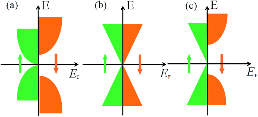 | ||
| Fig. 1 Schematic rule for designing HDSs. (a) SGSs, (b) Dirac semimetals, and (c) HDSs. The Dirac point of HDSs is exactly located at the Fermi level, unlike that of SGSs. Owing to the intersection of the Dirac-like node and the Fermi level, HDSs represent the real gapless properties rather than half-metals in one spin channel. | ||
Dirac semimetal is a new type of quantum state with non-trivial topological properties. Its body energy band generally has a three-dimensional Dirac point near the Fermi surface. The representative example is monolayer graphene composed of a purely 2D honeycomb network of carbon atoms.27,29 Low-energy excitation in graphene is governed by π electrons in 2p orbitals, whose energy dispersion has linear band crossings with the Dirac-like node at the Fermi level, called the Dirac cones. It exhibits unique electronic properties such as ballistic charge transport,30 high carrier mobility,31 and the quantum Hall effect.32 Subsequently, many 2D lattices such as germanene,33 carbon allotropes,34–37 boron allotropes,38 SiC3,27 and C4N,39 have been identified as Dirac materials. However, the Dirac cone in these materials is intrinsically spin-degenerated, which actually limits its utilization in massless spintronics. Thus, the investigation of the controllability of the band crossings and topological phases by using the p-orbital degrees of freedom is desirable, but such an interesting possibility has rarely been investigated.
The ultimate goals for future spintronic devices are to require ultra-fast transport and ultra-lower energy consumption, that is, eliminating the effective mass of electrons or holes and enabling massless charges to be completely spin-polarized. In comparison with parabolic-like SGSs (Fig. 1(a)) and four-degenerated band Dirac cones (Fig. 1(b)), Dirac-like SGSs, termed HDSs, as illustrated in Fig. 1(c), are the better class of magnetic materials for use in spintronic devices as HDSs possess more exotic spin and charge states. Thus, it is highly desirable to find stable HDSs with an intrinsic 100% spin-polarized Dirac state. Normally, HDSs can be divided into two types: type-I, the d-state HDSs, in which the Dirac state is contributed by the d-orbital of transition-metal atoms, and type-II, the p-state HDSs, whose states are from the p-orbital of transition-metal atoms. To date, the majority of reported HDS members belong to type-I HDSs,39–47 while there has been barely any reports on 2D type-II HDS materials. It is highly desirable to design type-II HDSs with robust spin ordering and a high Curie temperature simultaneously, which may make experimental synthesis largely accessible.
Meanwhile, among the 2D materials family, 2D Kagome lattices have been attracting great interest due to their rich properties. Most members of the family are carbides and oxides (e.g., Be3C2, V2O3, Nb2O3, and LiFeSe),40–45 consisting of one flat layer with D6h symmetry. Considering that nitrogen has one electron more than the oxygen atom, it is natural to ask whether transition-metal nitrides can also be stabilized in a 2D crystal Kagome lattice. If so, this may open the door to a new family of 2D materials, i.e., 2D Kagome transition-metal nitrides, which will also grow into a big family with fascinating quantum properties.
In this work, we try to address the above challenge and question by proposing a new family of 2D transition-metal nitrides with the Kagome structure. Based on first-principles calculations, we show that Cd2N3 can be stabilized in this 2D lattice as shown in Fig. 2(a), which is dynamically and thermally stable. Monte Carlo simulations on the basis of the 2D Heisenberg Hamiltonian model show that the Curie temperature TC = 225 K, having potential for high temperature applications. The coexistence of fully spin-polarization and linear dispersion Dirac states can be realized in Cd2N3, which features ultra-clean energy dispersion and ultra-high Fermi velocity. Distinguished from most proposed nonmagnetic Dirac materials, the four-fold degeneracy neck crossing-point traces out two-fold degeneracy lines emerged in the single-spin channel and the profile of HDSs is revealed by a tight-binding (TB) model. To the best of our knowledge, the Cd2N3 monolayer represents the first example that hosts the 2D HDS in the equilibrium state. When turning on the spin–orbit coupling (SOC), Cd2N3 becomes a quantum anomalous Hall (QAH) insulator with its energy gap of Eg = 5.0 meV, larger than recently predicted Eg = 2.3 meV in Mn-DCA,38 which is characterized by the nonzero Chern number (C = 1) and chiral edge states. In comparison to Cr- or V- doped (Bi, Sb)2Te3 film,s such a lattice without any magnetic doping is easier to synthesize and has much higher homogeneity. Thus, our discovery not only predicts a family of new 2D HDS materials, which vastly enriches the SGS family, but also provides an experimentally feasible platform to explore the new emergent QAH effect and their fascinating fundamental physical effects.
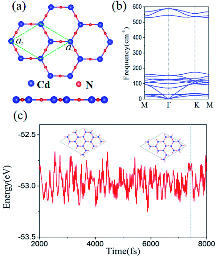 | ||
| Fig. 2 (a) Top and side views with lattice vectors a1 and a2 in the x–y plane. Rhombus shows the unit cell. (b) Calculated phonon spectrum of Cd2N3. (c) MD simulations at temperature 300 K. | ||
2. Computational details and method
All the spin-polarized calculations are performed by using density-functional theory (DFT), as implemented in the Vienna ab initio simulation package (VASP).46 The projector-augmented-wave (PAW) potential,47,48 Perdew–Burke–Ernzerhof (PBE) exchange-correlation functional49 and plane-wave basis with a kinetic energy cutoff of 500 eV are employed. An all-electron description, the projector augmented wave method, is used to describe the electron-ion interaction. The Brillouin zone is sampled by using a 9 × 9 × 1 Gamma-centered Monkhorst–Pack grid, and the SOC is included by a second variational procedure on a fully self-consistent basis. During structural optimization, all atomic positions and lattice parameters are fully relaxed, and the maximum force allowed on each atom is less than 0.02 eV Å−1. Spin polarization is included through all the calculations. Since standard DFT may fail to describe the magnetism, the Heyd–Scuseria–Ernzerhof (HSE06) functional54 has been carried out to examine the magnetism and electronic structures. Phonon dispersion is calculated using the finite displacement method, as implemented in the PHONOPY code.553. Results and discussion
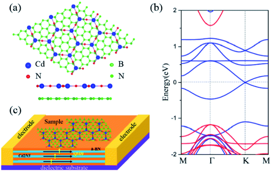
Because most elements and compounds are not favorable to directly form a 2D Kagome lattice, we propose a new transition-metal nitride, Cd2N3, to substitute the Kagome lattice, as illustrated in the top and side views of Fig. 2(a). The Cd2N3 monolayer forms a honeycomb lattice with a point symmetry of D6h by sharing one nitrogen (N) bridge with each neighbor, reminiscent of the crystal structure in the 2D organic Mn-DCA lattice.50–53,57,58 The optimized lattice parameters for Cd2N3 are a1 = a2 = 7.29 Å, and three N atoms locate around each Cd atom and the bond angle N–Cd–N is 120°, with a Cd–Cd distance of d = 4.21 Å. To characterize the thermodynamic stability of Cd2N3, we calculate the cohesive energy ΔEf defined as| Ef = E (Cd2N3) − 2μ (Cd) −3/2μ (N2) | (1) |
It is important to examine whether the experimentally fabricated Cd2N3 is stable and whether the magnetic state survives at room temperature. To test the kinetic stability of Cd2N3, we perform phonon spectrum calculations for Cd2N3, as shown in Fig. 1(b). Apparently, there is no imaginary mode in the whole Brillouin zone, indicating that the Cd2N3 lattice is dynamically stable. Additionally, the thermal stability of the Cd2N3 lattice is assessed by performing ab initio molecular dynamics (MD) simulations. We use a 4 × 4 supercell to carry out the individual simulations at a temperature of 300 K. As seen from Fig. 2(c), the crystal structure of Cd2N3 does not collapse throughout 8 ps MD simulation. In fact, Wang et al56 reported that the Y2O3 lattice forms a complete monolayer on platinum-supported graphene. The Y2O3 monolayer interacts weakly with graphene, but is stable at high temperature. Scanning tunnelling microscopy reveals that Y2O3 exhibits a 2D hexagonal lattice rotated by 30° relative to the hexagonal graphene lattice. The above results reveal that the Cd2N3 monolayer has very good thermal stability and could possibly be prepared in the experiment and survive at room temperature.
We now focus on the magnetic structures of Cd2N3. Spin-polarized results reveal a spin moment of 5.0 μB per cell as a result of large Hund's rule, which can be further illustrated by spin-polarized electron density, Δρ = ρ↑ − ρ↓, the difference between the electron densities of two spin channels, shown in the inset in Fig. 3(c). A large amount of spins is localized at the N site (∼1.21 μB) with a slight contribution from the Cd ion (∼0.08 μB), indicating that the N ions mainly contribute to magnetism, also verified by Bader charge analysis.61 As is known, the Mermin–Wagner theorem62 reveals that the long-range magnetic ordering is absent by thermal fluctuations in 2D lattices. However, it doesn't hold true for all 2D structures, especially for strong anisotropy cases.16,17 Thus, to determine the magnetic ground state of Cd2N3, we consider several possible configurations, including, FM, Neel antiferromagnetic (NAFM), stripe AFM (SAFM), and zigzag AFM (ZAFM), as shown in Fig. 3(a). The calculated results indicate that the FM state (ΔEFM = EFM − EAFM) is energetically 14.43, 12.41, 9.75, and 9.32 meV N−1 lower than the NAFM, SAFM, and ZAFM states, respectively. Furthermore, we also check the spin configuration of the coplanar 120° AFM state, and find that the Cd2N3 monolayer prefers energetically FM (ΔEFM = 16.58 meV N−1) states.
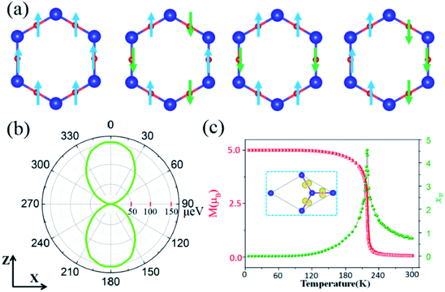 | ||
| Fig. 3 (a) Possible spin configurations of the Kagome Cd2N3 lattice: FM, NAFM, SAFM, and ZAFM. (b) Angular dependence of the MAE (θ, φ) with the direction of magnetization lying on three different planes. The inset illustrates that the spin vector S on the x–y, y–z, and x–z planes is rotated with an angle θ around x, y, and z axis, respectively. (c) MC simulations of the average magnetic moment and spin susceptibility per unit cell with respect to temperature. The electron density of two spin channels for FM spin configuration is defined as 0.001 eV Å−3. | ||
Magnetocrystalline anisotropy energy (MAE), defined as the required energy to rotate the magnetization from an easy axis to hard axis of a ferromagnet and determines the difficulty of spin flipping, plays a key role in establishing 2D FM ordering. For a Kagome lattice, MAE (θ, φ) at an arbitrary direction (θ, φ) follows
MAE (θ, φ) = K1![[thin space (1/6-em)]](https://www.rsc.org/images/entities/char_2009.gif) cos2θ +K2cos4θ+K3cos43φ cos2θ +K2cos4θ+K3cos43φ | (2) |
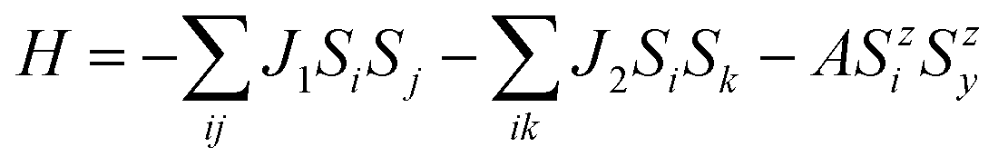
The Curie temperature (Tc) is a key parameter for the practical application of spintronic devices. Therefore, it is necessary to understand the behavior of magnetism with temperature before implementing Cd2N3 into practical spintronic devices. On the basis of the 2D Heisenberg model, the spin Hamiltonian can be expressed as
 | (3) |
Having determined the magnetic ground state of the Cd2N3 monolayer, we present the representative band structures without SOC, as shown in Fig. 4(a), where the blue and red colors display the spin-up and spin-down channels, respectively. One can see that both the spin-up and spin-down channels are completely split away from each other. Remarkably, the spin-up channel possesses a very large band gap 2.88 eV, whereas the spin-down one did not show a gap. Thus the charge transport is dominated by the spin-down electron, and the current flow in such a system should be fully spin-polarized, which is consistent with the case in Fig. 1(a). The band character can be further confirmed by the HSE06 method, which has a larger band gap of 3.56 eV in the spin-up channel. Though the bulk gap is enhanced for HSE06, the HDS bands are not altered near the Fermi level, indicating the robustness of the band character against the computational method. As EF lies almost in the middle of the spin gap, fully spin-polarized spin-filter efficiency can be maintained in a wide positive or negative bias range, rendering Cd2N3 an attractive candidate for spin-injection.
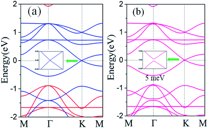 | ||
| Fig. 4 The energy bands along the high-symmetry lines without (a) and with SOC (b), respectively. The spin-up and spin-down bands are colored in red and blue, respectively. The Fermi level is set to zero. | ||
The most prominent findings on band dispersion are that in the spin-up channel, there are two several energy band crossings near EF, as shown Fig. 5(a), which mainly originates from the representation of the D6h point group. From the 3D band profile near the K point, accompanied by symmetry analysis, we can obtain the six Dirac-like nodes located exactly at the Fermi level. Notably, this is a typical Kagome band around the Fermi level, consisting of a completely flat band above two Dirac bands remaining at the K point. From the two linear bands in Fig. 5(a), the Fermi velocity vF of the carriers can be evaluated using linear fitting, ћvF ≈ dE(k)/dk. The obtained vF = 4.3 × 10⁵ m s−1 for Cd2N3 is comparable to that of graphene (8.2 × 10⁵ m s−1),64 and silicene (5.3 × 10⁵ m s−1).65 To understand the origin of Dirac states in Cd2N3, we calculate the orbital-resolved band structures, as shown in Fig. 6. One can see that the wave functions at the Fermi level are mainly from the N-2pz orbital with a slight contribution from Cd atoms, so there is no sp2 hybridization occurring on Cd2N3. The linear crossing Dirac states by the N-pz orbital is consistent with the pz Dirac state due to the nature of weak π bonds.66 Namely, Cd2N3 is a superior candidate of single-spin p-band Dirac materials for high-speed spintronic devices.
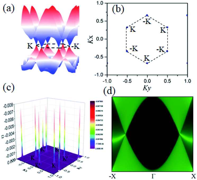 | ||
| Fig. 5 (a) The calculated 3D energy bands. (b) Berry curvature with SOC in 2D momentum space. The red-white-blue colors give the distribution of Berry curvature from positive to negative values, and the black dashed lines show the first BZ. (c) Distribution of the normalized Berry curvature over the BZ. (d) Chiral edge states of the Cd2N3 monolayer. | ||
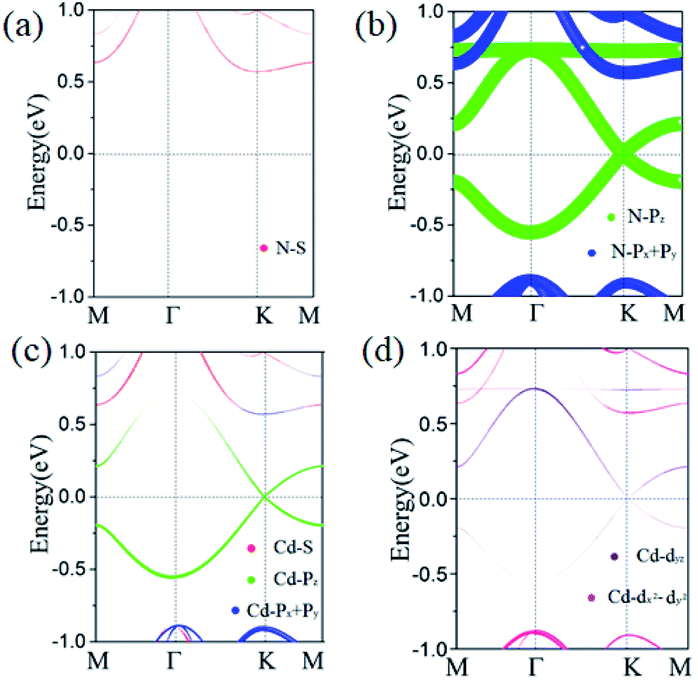 | ||
| Fig. 6 Orbital-resolved band structures for (a) N-s (b) N-p, (c) Cd-d, and (d) Cd-s states, respectively. | ||
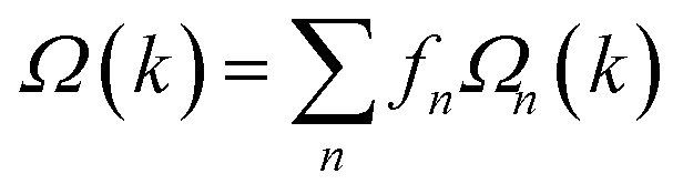
The peculiar band crossings that we found can host topologically nontrivial states in the presence of effective SOC. Fig. 3(b) shows the band structure with SOC, with a gap of Eg = 5.0 meV at the Dirac-like node. The band gap is similar to the case of 2D Mn-DCA (Eg = 2.3 meV),44 but smaller than recently predicted Eg = 20 meV in Cs2Mn3F12.43 It is noteworthy that, due to the small atomic numbers, SOC has negligible effect on the band structure of Cd2N3. Such band gap opening at the K point suggests a topologically nontrivial feature, which can be confirmed by the Berry curvature Ω(k) from the Kubo formula67–69 expressed as
 | (4) |
 | (5) |
 | (6) |
One can see that C = 1 with each Dirac cone contributing 0.5, characterizing the topological nature of the gaped state. So the anomalous Hall conductivity σxy, σxy = Ce2/h, shows a quantized charge Hall plateau at a value of e2/h located in the insulating gap of the spin-up Dirac-like node. Such a nonvanishing Chern number C = 1 and quantized Hall conductivity in Cd2N3 characterize the QAH effect.
The two band degeneracy point and the associated band topology can be well modeled by the TB model, taking the D6h lattice symmetry constraint into account. We introduce a Slater–Koster type TB model73 with the p orbital on the Kagome lattice formed by N atoms. The energy bands near the Dirac points can be expressed by the effective Hamiltonian
| H = ℏvF(kxτzσx + kyσy) + mHσzτz, | (7) |
SOC connects the electron spin and orbital degrees of freedom. So the crystal potential in 2D materials can be approximated by the spherical atomic potential, which gives on-site contribution to the TB Hamiltonian. By averaging the radial degree of freedom, the SOC reads
 | (8) |
![[s with combining right harpoon above (vector)]](https://www.rsc.org/images/entities/i_char_0073_20d1.gif) is the vector of the Pauli matrices representing the real spin and
is the vector of the Pauli matrices representing the real spin and ![[L with combining right harpoon above (vector)]](https://www.rsc.org/images/entities/i_char_004c_20d1.gif) is the angular momentum operator. The matrix element <⋯>μ,ν is given on the basis of directed atomic orbitals μ,ν and ξ
is the angular momentum operator. The matrix element <⋯>μ,ν is given on the basis of directed atomic orbitals μ,ν and ξ![[small script l]](https://www.rsc.org/images/entities/i_char_e146.gif) is the angular momentum resolved atomic SOC strength with
is the angular momentum resolved atomic SOC strength with ![[small script l]](https://www.rsc.org/images/entities/char_e146.gif) = {s,p,d,…}. Obviously, the energy bands are gapped by the effective SOC, which requires nonzero sz due to its out-of-plane magnetic moment in the Cd2N3 monolayer. Thus, our TB analysis provides a systematic understanding of the existing first-principles results, and furthermore, a useful guide for further material exploration.
= {s,p,d,…}. Obviously, the energy bands are gapped by the effective SOC, which requires nonzero sz due to its out-of-plane magnetic moment in the Cd2N3 monolayer. Thus, our TB analysis provides a systematic understanding of the existing first-principles results, and furthermore, a useful guide for further material exploration.
The derived Haldane effective model describes the QAH effect,70 and the existence of topologically protected chiral edge states is one of the most important signatures of the QAH effect. To reveal the nontrivial topological nature of the Cd2N3 lattice, we construct Green's functions71 for the semi-infinite boundary based on the maximally localized Wannier function method.72,73Fig. 4(d) shows the local density of states (LDOSs) of the edge states. Obviously, the nontrivial edge states connecting the CB and VB cross the insulating gap of the spin-up Dirac cone, consistent with the Chern number C = 1. The spin-polarized Dirac-fermion mediated topological character suggests that the Cd2N3 monolayer is intrinsic, holding the potential QAH phase.
As is well known, the physical properties of 2D materials can be effectively tuned by strain, like the band gap engineering of 2H-TMD semiconductors.74 Strain has also been proposed to effectively modulate dielectric properties,75 SOC,76 thermal conductivity77 and interlayer coupling in vdW heterostructures (HTSs)78 in 2D lattices. In the following, we will show that strain can induce SOC induced bulk gaps and spin-exchange interactions. Fig. 7 presents the evolution of direct gap Eg and FM exchange energy as a function of strain ε, defined as ε = (a − a0)/a0, where a (a0) is the strained (equilibrium) lattice constants. Note that the nontrivial topological states remain within the strain range of 10%. This suggests that Cd2N3 maintains a topologically nontrivial state, which is stable against external strains. The gap Eg decreases slightly with tensile strains, becoming Eg = 4.95 meV under strain 10%. Additionally, the variation of total energies of the FM and AFM states (ΔEFM = EFM − EAFM) with biaxial strains is presented. The results show that the FM ground state of Cd2N3 is robust against strains. The exchange energy also decreases slightly with increasing tensile strains, for example, when ε = 10%, ΔEFM = 14.43 meV, leading to less changes of TC. The dependency of TC onstrain is clearly different from the cases of 2D FeCl2 (ref. 50) and CdSe2,51 where TC changes sensitively with respect to external strains. So we can infer that Cd2N3 may be a promising intrinsic high-temperature spintronic material. Here we must note that previously proposed strategies to realize p-band FM ordering may be hard to be experimentally controllable, because a strong external electric field or carefully selective doping is required. Our work thus reports the first intrinsic p-band HDS material, even though the experimental synthesis of Cd2N3 may still remain a challenge. As these magnetic materials potentially offer large spin relaxation times due to small SOC,79 our results highlight a new promising material for experimental validation studies toward the realistic p-band spintronics applications.
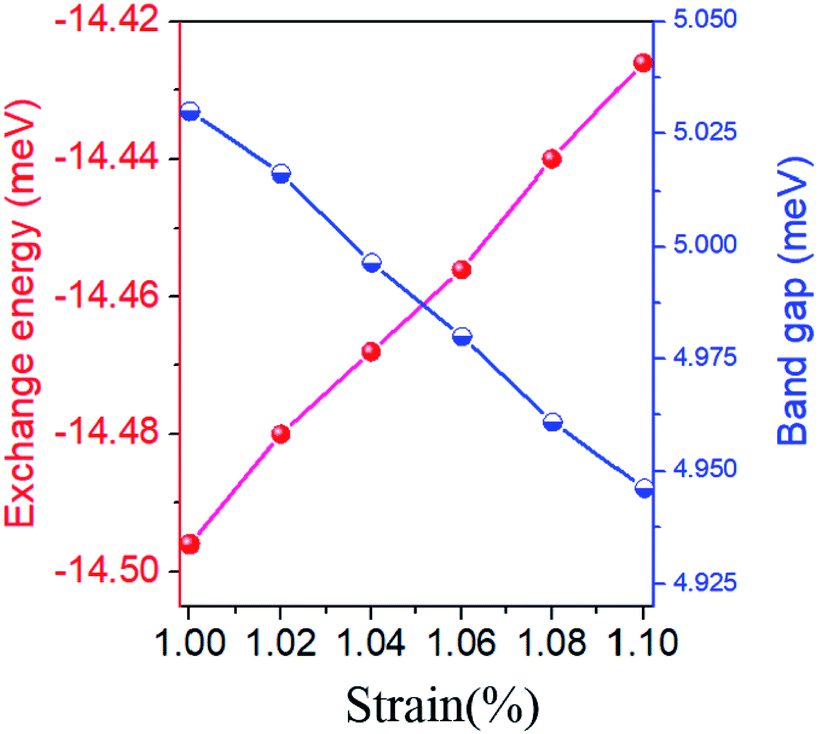 | ||
| Fig. 7 The variations of the global gap and exchange energy as a function of biaxial strains. | ||
Finally, one critical point is whether the QAH effect of 2D Cd2N3 can remain on a substrate, since the substrates are inevitable in device applications.80,81 As is known, the BN monolayer is chemically inert and does not easily bond strongly with other atoms, and thus may be adopted as a protective film to grow Cd2N3. So, the Cd2N3/BN HTS has been constructed, as shown in Fig. 8(a). Structural optimization indicates that the distance of Cd2N3 and BN layers is 3.10 Å with a binding energy of −34 meV per unit cell, a typical van der Waals structure. In this case, the main features of the QAH effect in the Cd2N3 lattice remain intact. Fig. 8(b) presents the calculated band structure with SOC. As expected, here there is still a SOC-induced gap at the Dirac point around the Fermi level, and the states around the Fermi level are dominantly contributed by the Kagome Cd2N3 band. Given that the 2D BN substrate electrically insulates the adjacent QSH layer of Cd2N3, protecting parallel helical edge channels from being gapped by interlayer hybridization, Cd2N3/BN is an ideal HTS to support the dissipationless charge/spin transport in the quantum device. This demonstrates the feasibility of constructing the quantum device with the Cd2N3/BN heterostructure, as illustrated in Fig. 8(c).
 | ||
| Fig. 8 (a) Top and side views of the epitaxial growth of the Cd2N3 lattice on the BN substrate. The interlayer distance is 3.10 Å. (b) The corresponding energy band structure of Cd2N3/BN HTS. (c) Schematic device model for proposed Cd2N3/h-BN heterostructure for quantum state measurement. Vertical arrows show the spin orientation of electrons in the edge states and horizontal arrows show their transport directions. | ||
4. Conclusion
In summary, we employ first-principles calculations to demonstrate the possibility of realizing HDSs in Kagome lattices with TC = 225 K, which is much higher than that of the reported monolayers CrI3 (TC = 45 K) and Cr2Ge2Te6 (TC = 20 K). The inclusion of SOC can turn Cd2N3 into a QAH insulator, with a sizable band gap of Eg = 5.0 meV. Notably, the nontrivial topology is robust against biaxial strain with its band gap reaching up to Eg = 4.95 meV under strain 10%. Also, the TB model is constructed to clarify the origin of the HDS and nontrivial electronic properties. Considering that Cd2N3 enjoys good stability and excellent flexibility, our findings would stimulate further material exploration toward the HDS matter in Kagome materials. These outstanding properties of Cd2N3 indicate that it is a promising 2D material for potential application in designing energy efficient spintronic devices.Additionally, the proposed Cd2N3 is likely to be synthesized by molecular beam epitaxy (MBE) or by the chemical vapor deposition method. We can synthesize Cd2N3 with a synthesis method similar to that of Nb2O3.82 The QAH effect can be probed by scanning probe spectroscopy, ARPES, and ultimately by device fabrications and charge transport measurements. Thus, it offers a new platform for the study of the QAH effect in Kagome lattices for realizing low-dissipation spintronic devices, which is of significant fundamental importance.
Conflicts of interest
There are no conflicts to declare.Acknowledgements
This work was supported by the Taishan Scholar Program of Shandong Province (No. ts20190939), the National Natural Science Foundation of China (Grant No. 11804116 and 62071200) and the Natural Science Foundation of Shandong Province (No. ZR2018MA033).References
- S. A. Wolf, D. D. Awschalom, R. A. Buhrman, J. M. Daughton, S. von Cdolnár, M. L. Roukes, A. Y. Chtchelkanova and D. M. Treger, Science, 2001, 294, 1488 CrossRef CAS.
- C. W. Zhang and S. S. Yan, Appl. Phys. Lett., 2009, 95, 232108 CrossRef.
- R. A. de Groot, F. M. Mueller, P. G. van Engen and K. H. J. Buschow, Phys. Rev. Lett., 1983, 50, 2024 CrossRef CAS.
- H. Van Leuken and R. A. De Groot, Phys. Rev. Lett., 1995, 74, 1171 CrossRef CAS.
- K. W. Lee and C. E. Lee, Adv. Mater., 2012, 24, 2019–2023 CrossRef CAS.
- D. Hsieh, D. Qian and L. Wray, et al. , Nature, 2008, 452, 970 CrossRef CAS.
- Y. Xia, D. Qian and D. Hsieh, et al. , Nat. Phys., 2009, 5, 398 Search PubMed.
- Y. S. Hor, A. Richardella and P. Roushan, et al. , Phys. Rev. B, 2009, 79, 195208 CrossRef.
- D. Hsieh, Y. Xia and D. Qian, et al. , Phys. Rev. Lett., 2009, 103, 146401 CrossRef CAS.
- H. Ohno, A. Shen and F. Matsukura, et al. , Appl. Phys. Lett., 1996, 69, 363–365 CrossRef CAS.
- H. Kimura, T. Fukumura and M. Kawasaki, et al. , Appl. Phys. Lett., 2002, 80, 94–96 CrossRef CAS.
- A. Ramasubramaniam and D. Naveh, Phys. Rev. B, 2013, 87, 195201 CrossRef.
- K. Mullen, B. Uchoa and D. T. Glatzhofer, Phys. Rev. Lett., 2015, 115, 026403 CrossRef.
- C. Fang, Y. Chen, H.-Y. Kee and L. Fu, Phys. Rev. B, 2015, 92, 081201(R) CrossRef.
- R. W. Zhang, Z. Zhang and C. C. Liu, et al. , Phys. Rev. Lett., 2020, 124, 016402 CrossRef CAS.
- B. Huang, G. Clark, E. N. Moratalla, D. R. Klein, R. Cheng, K. L. Seyler, D. Zhong, E. Schmidgall, M. A. Mcguire and D. H. Cobden, Nature, 2017, 546, 270 CrossRef CAS.
- C. Gong, L. Li, Z. Li, H. Ji, A. Stern, Y. Xia, T. Cao, W. Bao, C. Wang and Y. Wang, Nature, 2017, 546, 265 CrossRef CAS.
- X. L. Wang, Phys. Rev. Lett., 2008, 100, 156404 CrossRef CAS.
- G. D. Liu, X. F. Dai and H. Y. Liu, et al. , Phys. Rev. B, 2007, 77, 014424 CrossRef.
- S. Skaftouros and K. Ozdogan, et al. , Appl. Phys. Lett., 2013, 102, 022402 CrossRef.
- G. Y. Gao and K. L. Yao, Appl. Phys. Lett., 2013, 103, 232409 CrossRef.
- Z. F. Wang, S. Jin and F. Liu, Phys. Rev. Lett., 2013, 111, 096803 CrossRef CAS.
- Y. Pan and Z. Yang, Phys. Rev. B, 2010, 82, 195308 CrossRef.
- L. Bainsla, A. I. Cdallick and M. M. Raja, et al. , Phys. Rev. B, 2015, 92, 045201 CrossRef.
- F. Zheng, C. Zhang and P. Wang, et al. , J. Appl. Phys., 2013, 113, 154302 CrossRef.
- G. Gao, G. Ding and J. Li, et al. , Nanoscale, 2016, 8, 8986–8994 RSC.
- C. L. Kane and E. J. Mele, Phys. Rev. Lett., 2005, 95, 226801 CrossRef CAS.
- X. Zhou, R. W. Zhang and Z. Zhang, et al. , J. Phys. Chem. Lett., 2019, 10(11), 3101 CrossRef CAS.
- A. H. Castro Neto, F. Guinea, N. M. R. Peres, K. S. Novoselov and A. K. Geim, Rev. Mod. Phys., 2009, 81, 109–162 CrossRef CAS.
- Y. P. Bliokh, V. Freilikher and F. Nori, Phys. Rev. B, 2013, 87, 2451 CrossRef.
- K. S. Novoselov, A. K. Geim, S. V. Cdorozov, D. Jiang, M. L. Katsnelson, I. V. Grigorieva, S. V. Dubonos and A. A. Firsov, Nature, 2005, 438, 197–200 CrossRef CAS.
- Y. Zhang, Y. W. Tan, H. L. Stormer and P. Kim, Nature, 2005, 438, 201–204 CrossRef CAS.
- S. Cahangirov, M. Topsakal, E. Aktürk, H. Şahin and S. Ciraci, Phys. Rev. Lett., 2009, 102, 236804 CrossRef CAS.
- J. Chen, J. Xi, D. Wang and Z. Shuai, J. Phys. Chem. Lett., 2013, 4, 1443 CrossRef CAS.
- C. L. Xu, R. Z. Wang, M. S. Miao, X. L. Wei, Y. P. Chen, H. Yan, W. M. Lau, L. M. Liu and Y. M. Ma, Nanoscale, 2014, 6, 1113–1118 RSC.
- Z. Wang, X. F. Zhou, X. Zhang, Q. Zhu, H. Dong, M. Zhao and A. R. Oganov, Nano Lett., 2015, 15, 6182–6186 CrossRef CAS.
- H. Zhang, Y. Xie, Z. Zhang, C. Zhong, Y. Li, Z. Chen and Y. Chen, J. Phys. Chem. Lett., 2017, 8, 1707 CrossRef CAS.
- X. Qin, Y. Wu, Y. Liu, B. Chi, X. Li, Y. Wang and X. Zhao, Sci. Rep., 2017, 7, 10546 CrossRef.
- C. Pu, D. Zhou, Y. Li, H. Liu, Z. Chen, Y. Wang and Y. Ma, J. Phys. Chem. C, 2017, 121, 2669 CrossRef CAS.
- S. J. Zhang, C. W. Zhang, S. F. Zhang, W. X. Ji, P. Li, P. J. Wang, S. S. Li and S. S. Yan, Phys. Rev. B, 2017, 96, 205433 CrossRef.
- P. Zhou, Z. S. Mab and L. Z. Sun, J. Mater. Chem. C, 2018, 6, 1206–1214 RSC.
- Y. P. Wang, W. X. Ji, C. W. Zhang, P. Li, P. J. Wang, B. Kong, S. S. Li, S. S. Yan and K. Liang, Appl. Phys. Lett., 2017, 110, 233107 CrossRef.
- M. H. Zhang, X. L. Chen, W. X. Ji, P. J. Wang and C. W. Zhang, Appl. Phys. Lett., 2020, 116, 172105 CrossRef.
- Y. Y. Deng, Y. Song, Y. Zhang, J. Wang, N. Z. Sun, Z. Yi, Y. Wu, Y. Z. Wu, S. Zhu, J. Wang, J. Chen and X. H. Zhang, Nature, 2018, 563, 94–99 CrossRef CAS.
- C. Gong, L. Li, Z. Li, H. Ji, A. Stern, Y. Xia, T. Cao, W. Bao, C. Wang, Y. Wang, Z. Q. Qiu, R. J. Cava, S. G. Louie, J. Xia and X. Zhang, Nature, 2017, 546, 265 CrossRef CAS.
- B. Huang, G. Clark, E. N. Moratalla, D. R. Klein, R. Cheng, K. L. Seyler, D. Zhong, E. Schmidgall, M. A. McGuire, D. H. Cobden, W. Yao, D. Xiao, P. J. Herrero and X. Xu, Nature, 2017, 546, 270 CrossRef CAS.
- M. H. Zhang, C. W. Zhang, P. J. Wang and S. S. Li, Nanoscale, 2018, 10, 20226 RSC.
- X. J. Ni, W. Jiang, H. Q. Huang, K. H. Jin and F. Liu, Nanoscale, 2018, 10, 11901 RSC.
- L. Zhang, S. F. Zhang, W. X. Ji, C. W. Zhang, P. Li, P. J. Wang, S. S. Li and S. S. Yan, Nanoscale, 2018, 10, 20748 RSC.
- G. Kresse and J. Furthmüller, Phys. Rev. B, 1996, 54, 101169 CrossRef.
- P. E. Blöchl, Projector augmented-wave method, Phys. Rev. B, 1994, 50, 17953 CrossRef.
- G. Kresse and D. Joubert, Phys. Rev. B, 1999, 59, 1348 Search PubMed.
- J. P. Perdew, K. Burke and M. Ernzerhof, Phys. Rev. Lett., 1996, 77, 3865 CrossRef CAS.
- J. Paier, M. Cdarsman, K. Hummer, G. Kresse, I. C. Gerber and J. G. Ángyán, J. Chem. Phys., 2016, 124, 154709 CrossRef.
- A. Togo and I. Tanaka, Scr. Mater., 2015, 108, 1 CrossRef CAS.
- Z. F. Wang, Z. Liu and F. Liu, Nat. Commun., 2013, 4, 1471 CrossRef CAS.
- X. Zhang, Z. Wang, M. Zhao and F. Liu, Phys. Rev. B, 2016, 93, 165401 CrossRef.
- R. Addou, A. Dahal and M. Batzill, Nat. Nanotechnol., 2013, 8, 41 CrossRef CAS.
- B. Huang, G. Clark, E. Navarro-Moratalla, D. R. Klein, R. Cheng, K. L. Seyler, D. Zhong, E. Schmidgall, M. A. Mcguire and D. H. Cobden, Nature, 2017, 546, 270 CrossRef CAS.
- C. Gong, L. Li, Z. Li, H. Ji, A. Stern, Y. Xia, T. Cao, W. Bao, C. Wang and Y. Wang, Nature, 2017, 546, 265 CrossRef CAS.
- G. Henkelman, A. Arnaldsson and H. Jlonsson, Comput. Mater. Sci., 2016, 36, 354 CrossRef.
- N. D. Mermin and H. Wangner, Phys. Rev. Lett., 1966, 17, 1133 CrossRef CAS.
- M. Esters, R. G. Hennig and D. C. johnson, Phys. Rev. B, 2017, 96, 235147 CrossRef.
- Y. Jiao, F. Cda, J. Bell, A. Bilic and A. Du, Angew. Chem., 2016, 128, 10448–10451 CrossRef.
- Y. L. Wang and Y. Ding, Solid State Commun., 2013, 155, 6–11 CrossRef CAS.
- Z. X. Guo, S. Furuya, J. Iwata and A. Oshiyama, Phys. Rev. B, 2013, 87, 235435 CrossRef.
- Y. G. Yao, L. Kleinman, A. H. MacDonald, J. Sinova, T. Jungwirth, D. S. Wang, E. Wang and Q. Niu, Phys. Rev. Lett., 2004, 92, 037204 CrossRef.
- Y. G. Yao and Z. Fang, Phys. Rev. Lett., 2005, 95, 156601 CrossRef CAS.
- J. C. Slater and G. F. Koster, Phys. Rev., 1954, 94, 1498 CrossRef CAS.
- S. Konschuh, M. Gmitra and J. Fabian, Phys. Rev. B, 2010, 82, 245412 CrossRef.
- J. L. Lado and J. Fernández-Rossier, 2D Mater., 2017, 4, 035002 CrossRef.
- C. L. Kane and E. J. Mele, Phys. Rev. Lett., 2005, 95, 226801 CrossRef CAS.
- C. C. Liu, W. X. Feng and Y. G. Yao, Phys. Rev. Lett., 2011, 0107, 076802 CrossRef.
- P. Johari and V. B. Shenoy, ACS Nano, 2012, 6, 5449 CrossRef CAS.
- A. Kumar and P. K. Ahluwalia, Phys. B, 2013, 419, 66 CrossRef CAS.
- P. Koskinen, I. Fampiou and A. Ramasubramaniam, Phys. Rev. Lett., 2014, 112, 186802 CrossRef.
- Z. Ding, Q.-X. Pei, J.-W. Jiang and Y.-W. Zhang, J. Phys. Chem. C, 2015, 119, 16358 CrossRef CAS.
- M. Sharma, A. Kumar, P. K. Ahluwalia and R. Pandey, J. Appl. Phys., 2014, 116, 063711 CrossRef.
- S. Sanvito, Molecular spintronics, Chem. Soc. Rev., 2010, 40, 3336 RSC.
- S. S. Li, W. X. Ji, S. J. Hu, C. W. Zhang and S. S. Yan, ACS Appl. Mater. Interfaces, 2017, 9, 41443 CrossRef CAS.
- M. Zhou, Z. Liu, W. M. Ming, Z. F. Wang and F. Liu, Phys. Rev. Lett., 2014, 113, 236802 CrossRef.
- S. Q. Wang, C. Noguera and M. R. Castell, Phys. Rev. B, 2019, 100, 125408 CrossRef CAS.
| This journal is © The Royal Society of Chemistry 2021 |