
 Open Access Article
 This Open Access Article is licensed under a Creative Commons Attribution-Non Commercial 3.0 Unported Licence
Nanoimprinted conducting nanopillar arrays made of MWCNT/polymer nanocomposites: a study by electrochemical impedance spectroscopy†
Chuan
Xiao
 ,
Yuming
Zhao
and
Wei
Zhou
*
,
Yuming
Zhao
and
Wei
Zhou
*
Department of Electrical and Computer Engineering, Virginia Tech, Blacksburg, VA 24060, USA. E-mail: wzh@vt.edu
First published on 27th November 2020
Abstract
Conducting vertical nanopillar arrays can serve as three-dimensional nanostructured electrodes with improved electrical recording and electrochemical sensing performance in bio-electronics applications. However, vertical nanopillar-array electrodes made of inorganic conducting materials by the conventional nanofabrication approach still face challenges in terms of high manufacturing costs, poor scalability, and limited carrier substrates. Here, we report a new type of conducting nanopillar array composed of multi-walled carbon nanotube (MWCNT) doped polymeric nanocomposites, which are manufactured on the wafer-scale on both rigid and flexible substrates by direct nanoimprinting of perfluoropolyether nanowell-array templates into uncured MWCNT/polymer mixtures. By controlling the MWCNT ratios and the annealing temperatures during the fabrication process, MWCNT/polymer nanopillar arrays can be endowed with outstanding electrical properties with high DC conductivity (∼4 S m−1) and low AC electrochemical impedance (∼104 Ω at 1000 Hz). Moreover, by electrochemical impedance spectroscopy (EIS) measurements and equivalent circuit modeling analysis, we can decompose the overall impedance of the MWCNT/polymer nanopillar arrays in the electrolyte into multiple bulk and interfacial circuit components, and can thus illustrate their different dependences on the MWCNT ratios and the annealing temperatures. In particular, we find that an appropriate annealing process can significantly reduce the anomalous ion diffusion impedance and improve the MWCNT/polymer nanopillars' impedance properties in the electrolyte.
1. Introduction
Three-dimensional nanostructured electrodes based on conducting vertical nanopillar arrays have emerged as a useful tool in nano-bioelectronics for electrical recording of extracellular and intracellular membrane potentials1–5 as well as electrochemical sensing.6–9 Furthermore, recent studies have shown that living cells can engulf vertical nanopillar electrodes with a tight adhesion to improve electrical coupling at the cell–nanodevice interface.10,11 Also, dense arrays of nanopillar electrodes can be integrated with large-scale circuits to perform parallel electrical recording over the cellular network.12 In most previous studies, vertical nanopillar-array electrodes were made of inorganic conducting materials (e.g., Si, Au, and Pt) by conventional nanofabrication techniques using electron-beam lithography and focused ion beam milling, which faces difficulties in terms of high manufacturing costs, poor scalability, and limited choice of carrier substrates. Compared to conventional nanofabrication approaches, nanoimprint lithography exhibits unique advantages for low-cost scalable nanostructure manufacturing on rigid and flexible substrates.13–15 Very few studies, however, have been conducted to achieve the scalable nanoimprinting fabrication of conducting nanopillar arrays made of MWCNT/polymer nanocomposites, which can potentially feature appealing properties in terms of combined mechanical flexibility and strength as well as good (bio-)chemical stability and solvent resistance.16–22This work demonstrates the scalable nanoimprinting fabrication of conducting MWCNT/polymer nanopillar arrays, which possess high DC conductivity (∼4 S m−1) and low AC electrochemical impedance (∼104 Ω at 1000 Hz). In particular, wafer-scale conducting MWCNT/polymer nanopillar arrays can be manufactured by direct nanoimprinting of perfluoropolyether (PFPE) nanowell-array templates with high stiffness into uncured MWCNT/polymer mixtures. After the curing process, the hydrophobic PFPE nanowell-array templates can be separated from imprinted MWCNT/polymer nanopillar arrays. From 2D Raman mapping measurements, we observe that the distributions of MWCNTs are uniform on the scale of ∼25 × 25 μm2 but random in the sub-micrometer scale. Furthermore, we conduct 4-point probe DC conductivity measurements and AC electrochemical impedance spectroscopy (EIS) to investigate the effects of the MWCNT ratios and the annealing temperatures on the electrical properties of MWCNT/polymer nanopillar arrays. By equivalent circuit modeling and analysis, we can decompose the contributions to the overall EIS behaviors from different bulk and interfacial circuit elements. We reveal that the anomalous ion diffusion processes play a significant role in determining the EIS properties of MWCNT/polymer nanopillar arrays in the electrolyte.
2. Experimental
2.1 Materials and chemicals
Carboxyl functionalized MWCNTs with a diameter of 10–20 nm and length of 20–30 μm (purity > 95 wt%) were purchased from Cheap Tubes Inc., USA. The UV-curable polymer NOA83H, also containing the thermal curing catalyst, was supplied by Norland Product Inc., (USA). Sylgard-184 PDMS (Dow Corning) was obtained from Ellsworth Adhesives (USA). PFPE Fluorolink MD 700 was purchased from Solvay S.A. (Belgium). Photoinitiator 2-hydroxy-2-methylpropiophenone was obtained from Sigma-Aldrich (USA). The Silicon 3′′ P (100) 0–100 ohm cm SSP 406–480 μm Test Grade wafer was supplied by UniversityWafer Inc. (USA). (Tridecafluoro-1,1,2,2-tetrahydrooctyl)-1-tri (TFCOS) was obtained from UCT Specialties (USA).2.2 Fabrication of MWCNT/polymer nanopillar arrays
 | ||
| Fig. 1 Nanoimprinting conductive MWCNT/polymer nanocomposite NPAs. (A) Schematic illustration of nanoimprinting fabrication processes to create conductive NPAs of MWCNT/polymer composites by nanoimprinting. (B) Top-down view optical image of conductive MWCNT/polymer composite NPAs on a silicon substrate. (C) Optical image of bent conductive MWCNT/polymer composite NPAs on a flexible PET substrate. (D) Top view and cross-sectional view SEM images of conductive MWCNT/polymer composite NPAs. | ||
2.3 Characterization of MWCNT/polymer nanopillar arrays
 | (1) |
3. Results and discussion
3.1 Fabrication of MWCNT/polymer nanopillar arrays
 | ||
| Fig. 2 Raman characterization of conductive MWCNT/polymer composite NPAs. (A) Raman spectra of MWCNTs in a polymer matrix with a 25 × 25 μm area under 785 nm laser excitation. (B–D) Scanning confocal Raman intensity images of MWCNTs in a polymer matrix at (B) ID-band (1340 cm−1), (C) IG-band (1580 cm−1), and (D) (ID-band + IG-band)/2. (E) Histograms of Raman signal intensities of ID-band, IG-band, and (ID-band + IG-band)/2. (F) Scanning confocal Raman intensity images of the ratio of ID-band/IG-band. (G) ID-band and IG-band plotting corresponding to each pixel of Raman measurement. | ||
For statistical analysis of MWCNT spatial distributions, we plotted the histograms of ID, IG, and (ID + IG)/2 for 25 × 25 pixels across the 25 μm × 25 μm area on 20 wt% MWCNT/polymer nanopillar arrays (Fig. 2E), which shows several key points. First, the histogram plots for ID, IG, and (ID + IG)/2 all fit well to the normal distribution shape, indicating that the dispersion of MWCNTs is uniform on the scale of ∼25 × 25 μm2 despite the significant variations of the MWCNT concentration in the sub-micrometer scale. Second, the IG histogram shows a larger standard deviation (σ2 ∼ 4.85) than the ID histogram (σ2 ∼ 4.38) since the Raman peak of the in-plane graphene-like G-band in MWCNTs is more sensitive to the orientation variations for MWCNTs than the sp2-hybridized D-band from localized defects in MWCNTs. Third, the (ID + IG)/2 histogram shows an even smaller standard deviation (σ2 ∼ 3.28) by combining the Raman signals from both G-band and D-band contributions, thus providing a better estimation of the local concentrations for MWCNTs of different orientations compared to ID and IG.
Considering that IG from the in-plane G-band is much more sensitive to MWCNT orientations than ID from the sp2-hybridized D-band of localized defects, the spatial distribution of the ratiometric ID/IG values can reveal the spatial distribution of average MWCNT orientations in the polymer matrix. As shown in Fig. 2F, ID/IG values vary widely in the range from 0.1 to 10 with a random spatial distribution, reflecting a random orientation of MWCNTs embedded in MWCNT/polymer nanopillar arrays. Fig. 2G depicts the scatter plot of the relation between ID and IG from 25 × 25 pixels. The broad normal distribution of scatters centered near the position of (10, 10) reveals that the values of ID and IG from individual pixels have a relatively weak correlation with each other. Therefore, the spatial distributions of MWCNT concentrations, MWCNT defect densities, and MWCNT orientations are all random, and both ID and IG intensities are proportional to MWCNT concentrations.
3.2 Study of MWCNT/polymer nanopillar arrays with different MWCNT filling ratios
 | ||
| Fig. 3 Conductivity and EIS characterization of different MWCNT ratios of conductive MWCNT/polymer composite. (A) Results of conductivity of 20 points per sample calculated from the sheet resistance measured by 4 point probes of different MWCNT ratios. (B and C) EIS: (B) impedance and (C) phase results of different MWCNT ratios and different conductive MWCNT/polymer composite structures from 102 Hz to 105 Hz in pH = 7.4 PBS solution. | ||
Fig. 3C shows the spectra of the impedance phase angle for different MWCNT/polymer samples. For nanopillar array samples with 0, 5, and 10 wt% MWCNT ratios, as the frequency decreases from ∼105 Hz to ∼103 Hz, the impedance phase angle first increases and then slowly levels off; as the frequency further decreases from ∼103 Hz to ∼102 Hz, the impedance phase angle starts to fluctuate significantly in a random manner due to the longer travel distance of ions at the lower frequency range. For the nanopillar array with 20 wt% MWCNT ratio, as the frequency increases from ∼102 Hz to ∼104 Hz, the impedance phase angle increases from ∼−80° to the peak value of ∼−55°, and as the frequency further increases to ∼105 Hz, the phase angle reduces to ∼−81°. Unlike the 20 wt% MWCNT/polymer nanopillar arrays, 30 wt% MWCNT/polymer nanopillar arrays show a peak impedance phase angle of ∼−70° at ∼2 × 10⁴ Hz, and the flat MWCNT/polymer sample shows a peak impedance phase angle of ∼−10° at ∼1 × 10⁴ Hz.
 is the electrolyte resistance,
  is the bulk resistance of the MWCNT/polymer composite,
  includes all parasitic contact resistance and equipment resistance in the circuit,
  describes the bulk capacitance of the MWCNT/polymer composite, R2 is the charge transfer resistance at the interface between MWCNTs and the electrolyte, C2 is the double-layer capacitance at the interface between MWCNTs and the electrolyte, and Ma3 is the anomalous diffusion impedance for ion diffusion at the interface between MWCNTs and the electrolyte. In particular, the anomalous diffusion of ions is mainly caused by the nanoscale porous structures at the interface between MWCNT/polymer composites and the electrolyte.31,32 The diffusion of ions in the porous structure does not obey Fick's laws and thus cannot be modeled as a standard Warburg impedance term. By modifying Fick's equations and solving the differential equations under nanoporous boundary conditions, the anomalous diffusion impedance Ma3 can be expressed as33
 | (2) |
 | (3) |
 | ||
| Fig. 4 Analysis of different MWCNT ratios of conductive MWCNT/polymer composites. (A) Schematic equivalent circuit model. (B) Nyquist plots and equivalent circuit models of different MWCNT ratios and different conductive MWCNT/polymer composite structures from 102 Hz to 105 Hz in pH = 7.4 PBS solution. (C) The ratio plot of different fitting parameters to the conductive MWCNT/polymer flat composite reference for different MWCNT loadings of conductive MWCNT/polymer composites. (D) The plot of R2 and calculated Ma3 value of different MWCNT ratios and different structures of the conductive MWCNT/polymer composite from 102 Hz to 105 Hz. | ||
Fig. 4B depicts the Nyquist plots in the range between 103 and 105 Hz for different MWCNT/polymer samples. Based on the equivalent circuit modeling in Fig. 4A, we used the randomization method to fit equivalent circuit elements and produced fitting curves (dashed lines, Fig. 4B) in good agreement with measurements (discrete dots, Fig. 4B) for different samples. The randomization fitting methods start with some initial parameter values and randomize them to minimize χ2/|Z| in ohm. χ2/|Z| can be expressed as34
 | (4) |
 resistance for the MWCNT/polymer sample is in series with the electrolyte resistance
  and the remaining parasitic circuit/contact resistance
  ,
,  cannot be differentiated from
  and
and  in the fitting. Thus, the table does not include the circuit items for
  ,
,  , and
, and  .
.
| Condition | Circuit components | ||||||
|---|---|---|---|---|---|---|---|
| χ 2/|Z| | R 2 (Ω) | Rd3 (Ω) | Wd3 (rad s−1) | a 3 (a.u.) | C 2 (nF) |
|
|
| 20% flat | 0.43 | 17![[thin space (1/6-em)]](https://www.rsc.org/images/entities/char_2009.gif) 127 127 |
3.43 × 10⁶ | 0.061 | 0.999 | 2.712 × 10⁻² | 5.38 |
| 5% NPA | 0.358 | 125428 |
5.94 × 10⁸ | 0.050 | 0.989 | 0.164 | 0.54 |
| 10% NPA | 0.267 | 119300 |
4.67 × 10⁸ | 0.057 | 0.995 | 0.157 | 1.62 |
| 20% NPA | 0.052 | 3654 | 2.22 × 10⁶ | 0.070 | 0.806 | 0.618 | 6.71 |
| 30% NPA | 0.031 | 3985 | 1.67 × 10⁶ | 0.085 | 0.885 | 1.141 | 1.18 |
As shown in Table 1, the 20 wt% MWCNT/polymer flat sample and the 20 wt% MWCNT/polymer nanopillar arrays share similar fitted values of anomalous diffusion impedance (including Rd3, t3, and α3) and MWCNT network capacitance ( ), indicating their similar fractal nanoporous structures as well as similar distribution and density properties of MWCNT networks. However, 20 wt% MWCNT/polymer nanopillar arrays show much smaller values for both charge transfer resistance (R2: ∼3653 Ω) and double-layer capacitance (C2: ∼0.618 × 10⁻⁹ F) than the 20 wt% MWCNT/polymer flat sample (R2: ∼17127 Ω, C2: ∼2.712 × 10⁻¹¹ F), reflecting the much larger active surface area to interact with the electrolyte environment in both faradaic and non-faradaic processes. The observation of very different R2 and C2 values between nanopillar array and flat samples of the same 20% MWCNT ratio suggests that the nanoimprinting process for creating nanopillar arrays may mechanically force more MWCNTs to penetrate out of their polymer matrix for direct interfacing with electrolytes. The impedance of a capacitor inversely depends on the frequency and can be expressed as
 | (5) |
 | (6) |
946 Ω, and the |Ma3| calculated using eqn (2) is 649.94 Ω. Therefore, |ZC2| is much larger than the summation of R2 and |Ma3|, which explains its frequency-insensitive impedance response between ∼3 × 10³ Hz and ∼1 × 10⁵ Hz (Fig. 3B). In contrast, for 20 wt% MWCNT/polymer nanopillar arrays at 105 Hz, |ZC2| is 9705 Ω, |Ma3| is 13882 Ω, and R2 is 3653 Ω. Since |ZC2| is smaller than the summation of R2 and |Ma3|, the impedance for 20 wt% MWCNT/polymer nanopillar arrays continuously decreases with increasing frequency (Fig. 3B).
To examine the effects of the MWCNT ratio on the electrochemical impedance properties for nanopillar arrays, we used the 20 wt% MWCNT/polymer flat sample as a reference to plot the fitted ratiometric values of equivalent circuit elements, including  for the MWCNT network capacitance, C2/C(ref)2 for the double-layer capacitance, R2/R(ref)2 for the charge transfer resistance, and Rd3/Rd(ref)3 for the anomalous diffusion impedance. In Fig. 4C, we can observe several key points. First, before reaching the percolation threshold, as the MWCNT ratio increases from 5 wt% to 10 wt%,
  increases from 0.10 to 0.30 by ∼3 times, C2/C(ref)2 slightly increases from 6.05 to 5.79,
  slightly decreases from 7.32 to 6.97, and
  decreases from 174.70 to 137.35. Therefore, for the disconnected MWCNTs in the polymer matrix, the change of MWCNT ratios does not significantly affect the values for the circuit elements at the interface with electrolyte environments (e.g., C2, R2, and Rd3). However, the bulk capacitance
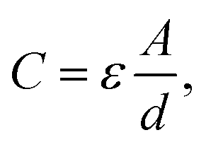
  can still increase significantly with the MWCNT ratio due to an increased electrode surface area (A) of MWCNTs and a reduced mean distance (d) between MWCNTs in the MWCNT/polymer composite, described by eqn (6). Second, as the MWCNT ratio increases from 10 wt% to 20 wt% across the percolation threshold,
  increases from 0.30 to 1.25, C2/C(ref)2 increases from 5.8 to 22.8 by ∼4 times,
  decreases from 6.97 to 0.21, and
  decreases from 137.4 to 0.65. In addition to the ∼4 times increase of interfacial and bulk capacitance
  and C2, reaching the percolation threshold can lead to a ∼35 times drop of R2 and a ∼210 times drop of Rd3, which suggests that the charge transport and ion diffusion processes at the electrolyte interface strongly depend on the formation of interconnected MWCNT networks. Third, after going beyond the percolation threshold, as the MWCNT ratio further increases from 20% to 30%,
  decreases from 1.25 to 0.22 by ∼5.7 times, C2/C(ref)2 increases from 22.78 to 42.07 by ∼2 times,
  slightly decreases from 0.21 to 0.17, and
  slightly decreases from 0.65 to 0.49. The significant drop for the bulk capacitance
  and relatively small changes for interfacial circuit elements of C2, R2, and Rd3 can be explained by the formation of MWCNT aggregations in the polymer matrix because of the poor dispersion of MWCNTs in the polymer matrix at very high MWCNT ratios (∼30%).
To investigate the relative contributions to the interfacial impedance between the charge transport term R2 and ion diffusion term Ma3, we compared the fitted impedance spectra for R2 (solid curves, Fig. 4D) and Ma3 (solid curves, Fig. 4D) for different samples. Unlike R2 which is independent of frequency changes, the impedance for Ma3 decreases with the frequency following eqn (2). Compared to the 20% MWCNT/polymer flat sample, the 20% MWCNT/polymer nanopillar arrays show a ∼45 times impedance increase for Ma3 but a ∼5 times impedance drop for R2 over the entire frequency range between 102 and 105 Hz (Fig. 4D). The smaller R2 for the nanopillar sample than the flat sample suggests that the mechanical forces during the nanostructured imprinting process can expose more electrochemically active MWCNTs on the surface of MWCNT/polymer nanopillar arrays in the electrolyte environment. On the other hand, the much larger Ma3 impedance for the nanopillar sample than the flat sample indicates that the nanoimprinting process can cause a higher degree of microscopic porosity on the surface of MWCNT/polymer nanopillar arrays to slow down the ion diffusion process at the interface with the electrolyte. For MWCNT/polymer nanopillar arrays with different MWCNT ratios, the impedance for Ma3 is dominant over R2 (Fig. 4D), revealing a faster rate of the faradaic electron charge transport process than the ion diffusion process in the tested frequency range between 102 and 105 Hz.
To access the sample uniformity in terms of EIS properties and the fabrication process reproducibility, we carried out EIS measurements at three different spots for each sample and three samples under each of the processing conditions (Fig. S-4, ESI†). We further fitted the EIS measurement results with the equivalent circuit model in Nyquist plots (Fig. S-5, ESI†). The fitted parameters show similar values (Table S-2, ESI†) between different spots on the same samples and between different samples under the same processing conditions, manifesting good sample uniformity and good fabrication reproducibility for making MWCNT/polymer NPAs.
3.3 Study of MWCNT/polymer nanopillar arrays with different annealing temperatures
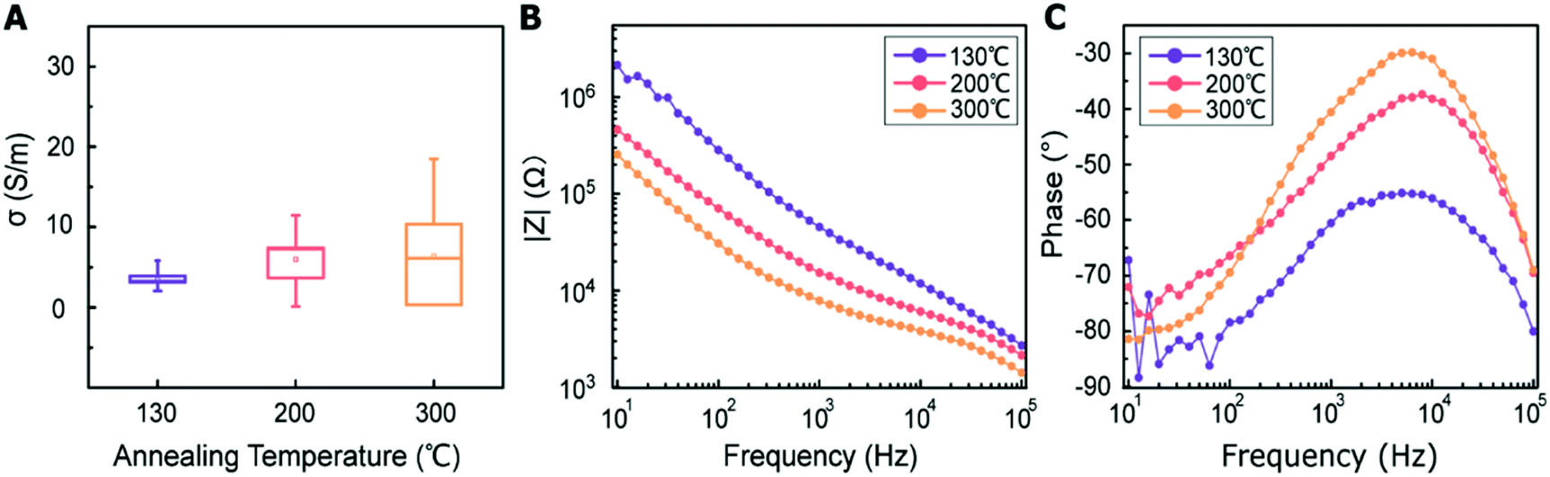 | ||
| Fig. 5 Conductivity and EIS characterization of annealing effect on 20 wt% conductive MWCNT/polymer composite NPAs. (A) Results of conductivity of 20 points per sample calculated from the sheet resistance measured by a 4 point probe of the annealing effect on a 20 wt% conductive MWCNT/polymer composite. (B and C) EIS: (B) impedance and (C) phase results of different annealing effects on the 20 wt% conductive MWCNT/polymer composite from 101 Hz to 105 Hz in pH = 7.4 PBS solution. | ||
 , C2/C(ref)2, R2/R(ref)2, and Rd3/Rd(ref)3 for 20 wt% MWCNT/polymer nanopillar arrays with different annealing temperatures (Fig. 6B).
 | ||
| Fig. 6 Analysis of the annealing effect on conductive MWCNT/polymer composite NPAs. (A) Nyquist plots and equivalent circuit model of conductive MWCNT/polymer composite NPAs with different annealing temperatures from 102 Hz to 105 Hz. (B) The ratio plot of different fitting parameters to the conductive MWCNT/polymer flat composite reference for different annealing temperatures on conductive MWCNT/polymer composite NPAs. (C) The plot of R2 and calculated Ma3 value of different annealing temperatures on conductive MWCNT/polymer composite NPAs from 102 Hz to 105 Hz. | ||
| Condition | Circuit components | ||||||
|---|---|---|---|---|---|---|---|
| χ 2/|Z| | R 2 (Ω) | Rd3 (Ω) | Wd3 (rad s−1) | a 3 (a.u.) | C 2 (nF) |
|
|
| 20% NPA 0 °C | 0.052 | 3653 | 2.22 × 10⁶ | 0.070 | 0.806 | 0.618 | 6.716 |
| 20% NPA 200 °C | 0.035 | 3451 | 1.57 × 10⁶ | 0.145 | 0.792 | 0.683 | 40.43 |
| 20% NPA 300 °C | 0.032 | 2525 | 2.78 × 10⁵ | 0.995 | 0.782 | 1.032 | 70.08 |

As the annealing temperature increases from 130 °C to 200 °C,  increases by ∼5 times from 1.25 to 7.51,
  decreases from 0.65 to 0.46, C2/C(ref)2 slightly increases from 22.79 to 25.40, and
  slightly changes from 0.21 to 0.20 (Fig. 6B). The significant increase of the bulk capacitance term
  indicates a reduced mean distance (d) between individual MWCNTs due to the self-relaxation and self-reorientation of MWCNTs in the softened polymer matrix at 200 °C, which agrees with the observation of increased conductivity from 4-probe measurements (Fig. 5A). The decrease of the anomalous diffusion term
  suggests a reduced nanoscale porosity at the interface between MWCNT/polymer nanopillar arrays and the electrolyte due to the annealing. The small changes of the double-layer capacitance term C2/C(ref)2 and charge transport resistance term
  indicate that the density of the interfacial MWCNTs exposed to the electrolyte does not change much with the annealing temperature increased from 130 °C to 200 °C.
As the annealing temperature further increases from 200 °C to 300 °C,  increases from 7.51 to 13.02,
  decreases by ∼6 times from 0.46 to 0.08, C2/C(ref)2 increases from 25.40 to 36.87, and
  decreases from 0.20 to 0.15 (Fig. 6B). Therefore, by using an even higher annealing temperature at 300 °C, the mean distance between individual MWCNTs can be further decreased to increase the bulk capacitance term
  , and the nanoscale porosity can also be reduced to decrease the ion diffusion impedance
  . Furthermore, the significant increase of the double-layer capacitance term C2/C(ref)2 and non-negligible decrease of the charge transport resistance term
  suggest an increased density of the interfacial MWCNTs exposed to the electrolyte, which may be due to the heat-induced rearrangement of the interfacial MWCNTs on the surface of MWCNT/polymer nanopillar arrays.
Fig. 6C compares the interfacial impedance contributions due to the charge transport term R2 and the anomalous ion diffusion term Ma3 for MWCNT/polymer nanopillar arrays with different annealing temperatures. First, by increasing the annealing temperature from 130 °C to 200 °C and 300 °C, the impedance for anomalous ion diffusion Ma3 can decrease by almost 2 orders of magnitude in the frequency range between 102 and 105 Hz, while the charge transport resistance R2 decreases by a much smaller factor. Second, although the impedance for Ma3 is dominant over R2 in the frequency range below 104 Hz, the difference of the impedance values between Ma3 and R2 can be significantly reduced by the annealing process at 300 °C. Therefore, an appropriate annealing process can help to reduce the overall impedance of MWCNT/polymer nanopillar arrays in (1) the bulk contributions from the resistance  and capacitance
  terms of MWCNT networks by softening the polymer matrix and reducing the mean distance between MWCNTs, (2) as well as the interfacial contributions from the anomalous ion diffusion Ma3 and charge transport R2 terms by smoothing the nanoporous structures and increasing the MWCNT densities exposed to the electrolyte.
4. Conclusion
In summary, we have developed a scalable, low cost, and high throughput nanoimprinting fabrication process to manufacture conducting MWCNT/polymer nanopillar arrays on the wafer-scale on both rigid and flexible substrates. We have conducted a systematic study to characterize and understand the dependence of the electrical properties of MWCNT/polymer nanopillar arrays on the MWCNT ratios and the annealing temperatures in the fabrication process. In particular, we find that both charge transport resistance and anomalous ion diffusion impedance at the electrolyte interface can decrease dramatically by increasing the MWCNT ratio over the percolation threshold to form interconnected MWCNT networks. Furthermore, we observe that MWCNT/polymer nanopillar arrays treated at annealing temperatures of 200 and 300 °C can have increased bulk conductivity, increased bulk capacitance, and reduced interfacial anomalous ion diffusion impedance. Compared to most nanopillar arrays made of inorganic conducting materials (e.g., Si, Au, and Pt) by conventional nanoengineering, nanoimprinting fabricated conducting MWCNT/polymer nanopillar arrays have unique advantages, such as combined mechanical flexibility and strength, roll-to-roll manufacturing scalability, and fabrication compatibility with both rigid and flexible substrates. Therefore, we envision that conducting MWCNT/polymer nanopillar arrays obtained by scalable nanoimprinting fabrication can open new opportunities in flexible wearable sensing devices, flexible implantable biosensors, and low-cost disposable biochips. Toward the use of conducting MWCNT/polymer nanopillar arrays for bioelectrical recording and electrochemical sensing, future research can explore the methods (1) for further improvement of the local dispersion uniformity of MWCNT networks in uncured polymer materials and (2) for scalable patterning, metallization, lift-off, and passivation processes to create many individually addressable recording sites composed of MWCNT/polymer nanopillar arrays.Conflicts of interest
There are no conflicts to declare.Acknowledgements
This work was supported by AFOSR Young Investigator Award FA9550-18-1-0328.References
- L. Hanson, Z. C. Lin, C. Xie, Y. Cui and B. X. Cui, Nano Lett., 2012, 12, 5815–5820 CrossRef CAS PubMed.
- J. T. Robinson, M. Jorgolli, A. K. Shalek, M. H. Yoon, R. S. Gertner and H. Park, Nat. Nanotechnol., 2012, 7, 180–184 CrossRef CAS PubMed.
- C. Xie, Z. L. Lin, L. Hanson, Y. Cui and B. X. Cui, Nat. Nanotechnol., 2012, 7, 185–190 CrossRef CAS PubMed.
- Z. L. C. Lin, C. Xie, Y. Osakada, Y. Cui and B. X. Cui, Nat. Commun., 2014, 5, 3206 CrossRef PubMed.
- J. Abbott, T. Y. Ye, L. Qin, M. Jorgolli, R. S. Gertner, D. Ham and H. Park, Nat. Nanotechnol., 2017, 12, 460–466 CrossRef CAS PubMed.
- C. Shin, W. Shin and H. G. Hong, Electrochim. Acta, 2007, 53, 720–728 CrossRef CAS.
- F. J. Rawson, M. T. Cole, J. M. Hicks, J. W. Aylott, W. I. Milne, C. M. Collins, S. K. Jackson, N. J. Silman and P. M. Mendes, Sci. Rep., 2016, 6, 37672 CrossRef CAS PubMed.
- M. Yang, S. B. Hong, J. H. Yoon, D. S. Kim, S. W. Jeong, D. E. Yoo, T. J. Lee, K. G. Lee, S. J. Lee and B. G. Choi, ACS Appl. Mater. Interfaces, 2016, 8, 22220–22226 CrossRef CAS PubMed.
- C. Lotwala and H. F. Ji, AIMS Mater. Sci., 2017, 4, 292–301 Search PubMed.
- W. T. Zhao, L. Hanson, H. Y. Lou, M. Akamatsu, P. D. Chowdary, F. Santoro, J. R. Marks, A. Grassart, D. G. Drubin, Y. Cui and B. X. Cui, Nat. Nanotechnol., 2017, 12, 750–756 CrossRef CAS PubMed.
- H. Y. Lou, W. T. Zhao, Y. P. Zeng and B. X. Cui, Acc. Chem. Res., 2018, 51, 1046–1053 CrossRef CAS PubMed.
- J. T. Robinson, M. Jorgolli, A. K. Shalek, M.-H. Yoon, R. S. Gertner and H. Park, Nat. Nanotechnol., 2012, 7, 180–184 CrossRef CAS PubMed.
- K. J. Byeon and H. Lee, Eur. Phys. J.: Appl. Phys., 2012, 59, 10001 CrossRef.
- L. J. Guo, Adv. Mater., 2007, 19, 495–513 CrossRef CAS.
- M. C. Traub, W. Longsine and V. N. Truskett, Annu. Rev. Chem. Biomol. Eng., 2016, 7, 583–604 CrossRef PubMed.
- J. Yu, K. Lu, E. Sourty, N. Grossiord, C. E. Koning and J. Loos, Carbon, 2007, 45, 2897–2903 CrossRef CAS.
- J. Fawaz, and V. Mittal, Polymer Nanotube Nanocomposite: A Review of Synthesis Methods, Properties and Applications, Polymer Nanotube Nanocomposites: Synthesis, Properties, and Applications, MA: Scrivener Publishing LLC, 2nd edn, 2014, pp. 25–27 Search PubMed.
- T. D. Prichard, S. S. Singh, N. Chawla and B. D. Vogt, Polymer, 2013, 54, 1130–1135 CrossRef CAS.
- S. Kundu, Y. Wang, W. Xia and M. Muhler, J. Phys. Chem. C, 2008, 112, 16869–16878 CrossRef CAS.
- Y. Guo, K. Ruan, X. Yang, T. Ma, J. Kong, N. Wu, J. Zhang, J. Gu and Z. Guo, J. Mater. Chem. C, 2019, 7, 7035–7044 RSC.
- A. Forcellese, M. Simoncini, A. Vita, A. Giovannelli and L. Leonardi, J. Mater. Process. Technol., 2020, 286, 116839 CrossRef CAS.
- M. Kumar, J. S. Saini and H. Bhunia, J. Mater. Eng. Perform., 2020, 29, 7511–7525 CrossRef.
- J. Henzie, M. H. Lee and T. W. Odom, Nat. Nanotechnol., 2007, 2, 549–554 CrossRef CAS PubMed.
- B. Bhushan, D. Hansford and K. K. Lee, J. Vac. Sci. Technol., A, 2006, 24, 1197–1202 CrossRef CAS.
- B. Technology, Four Point Probe Equations, http://four-point-probes.com/four-point-probe-equations/ Search PubMed.
- E. P. Dupont, R. Luisier and M. A. M. Gijs, Microelectron. Eng., 2010, 87, 1253–1255 CrossRef CAS.
- D. Qin, Y. Xia and G. M. Whitesides, Nat. Protoc., 2010, 5, 491 CrossRef CAS PubMed.
- J.-D. Cho, D.-P. Kim and J.-W. Hong, Open J. Org. Polym. Mater., 2014, 04(No. 01), 4 Search PubMed.
- L. Bokobza and J. Zhang, eXPRESS Polym. Lett., 2012, 6, 601–608 CrossRef CAS.
- F. Du, J. E. Fischer and K. I. Winey, Phys. Rev. B: Condens. Matter Mater. Phys., 2005, 72, 121404 CrossRef.
- Z. Pomerantz, G. Garcia-Belmonte, A. Joseph, J.-P. Lellouche, J. Bisquert and A. Zaban, Electrochim. Acta, 2007, 52, 6841–6847 CrossRef CAS.
- S. A. Tali, S. Soleimani-Amiri, Z. Sanaee and S. Mohajerzadeh, Sci. Rep., 2017, 7, 42425 CrossRef CAS PubMed.
- J. Bisquert and A. Compte, J. Electroanal. Chem., 2001, 499, 112–120 CrossRef CAS.
- BioLogic Science Instruments, Ec-lab Software User's Manual Version 10.1x, 2011 Search PubMed.
- B. H. Cipriano, A. K. Kota, A. L. Gershon, C. J. Laskowski, T. Kashiwagi, H. A. Bruck and S. R. Raghavan, Polymer, 2008, 49, 4846–4851 CrossRef CAS.
- H. Deng, T. Skipa, R. Zhang, D. Lellinger, E. Bilotti, I. Alig and T. Peijs, Polymer, 2009, 50, 3747–3754 CrossRef CAS.
Footnote |
| † Electronic supplementary information (ESI) available. See DOI: 10.1039/d0na00200c |
| This journal is © The Royal Society of Chemistry 2021 |