
 Open Access Article
 This Open Access Article is licensed under a
 Creative Commons Attribution 3.0 Unported Licence
Narrowband organic photodetectors – towards miniaturized, spectroscopic sensing
Yazhong
Wang†
 ,
Jonas
Kublitski†
,
Shen
Xing
,
Felix
Dollinger
,
Donato
Spoltore‡
,
Johannes
Benduhn
* and
Karl
Leo
*
,
Jonas
Kublitski†
,
Shen
Xing
,
Felix
Dollinger
,
Donato
Spoltore‡
,
Johannes
Benduhn
* and
Karl
Leo
*
Dresden Integrated Center for Applied Physics and Photonic Materials (IAPP) and Institute for Applied Physics, Technische Universität Dresden, Nöthnitzer Str. 61, 01187 Dresden, Germany. E-mail: johannes.benduhn@tu-dresden.de; karl.leo@tu-dresden.de
First published on 27th October 2021
Abstract
Omnipresent quality monitoring in food products, blood-oxygen measurement in lightweight conformal wrist bands, or data-driven automated industrial production: Innovation in many fields is being empowered by sensor technology. Specifically, organic photodetectors (OPDs) promise great advances due to their beneficial properties and low-cost production. Recent research has led to rapid improvement in all performance parameters of OPDs, which are now on-par or better than their inorganic counterparts, such as silicon or indium gallium arsenide photodetectors, in several aspects. In particular, it is possible to directly design OPDs for specific wavelengths. This makes expensive and bulky optical filters obsolete and allows for miniature detector devices. In this review, recent progress of such narrowband OPDs is systematically summarized covering all aspects from narrow-photo-absorbing materials to device architecture engineering. The recent challenges for narrowband OPDs, like achieving high responsivity, low dark current, high response speed, and good dynamic range are carefully addressed. Finally, application demonstrations covering broadband and narrowband OPDs are discussed. Importantly, several exciting research perspectives, which will stimulate further research on organic-semiconductor-based photodetectors, are pointed out at the very end of this review.
 Yazhong Wang | Yazhong Wang received his master degree from Linköping University, Sweden in 2017. In October 2017, he joined Dresden Integrated Center for Applied Physics and Photonic Materials (IAPP) at Technische Universität Dresden as a PhD student under the supervision of Prof. Dr Karl Leo. His research interests fall on exploring organic electronics for near-infrared sensing applications from exploring new material combinations to designing novel device architectures. |
 Jonas Kublitski | Jonas Kublitski obtained his master degree at Paraná Federal University in Brazil. In 2016, he joined the group of Prof. Dr Karl Leo at the Dresden Integrated Center for Applied Physics and Photonic Materials, where he pursued his PhD. During this period, he worked on organic photodetectors (OPDs), investigating fundamental mechanisms, such as dark current generation and photomultiplication in narrowband devices. Currently, he is a postdoctoral fellow in the same group. His research topics go towards the development of new OPD structures, formation of trap states and their relation with noise current in optoelectronic devices as well as charge carrier transport. |
 Shen Xing | Shen Xing received her BS and MS degree from the University of Electronic Science and Technology of China (UESTC). In October 2017, she started her PhD under the supervision of Prof. Dr Karl Leo at the Dresden Integrated Center for Applied Physics and Photonic Materials at Technische Universität Dresden. Her current research interests focus on high-performing organic photodetectors (OPDs) achieved by newly developed device structures and fabrication methods, aiming to facilitate OPDs to advanced sensor applications. |
 Felix Dollinger | Felix Dollinger received his diploma and PhD in physics from Technische Universität Dresden in Germany. He is specialized in organic electronics and has previously published on organic solar cells as well as organic transistors. Recently he focuses on material development for organic photodetectors. One of his main research goals is the development of stable and sustainable organic electronic devices that will enable previously impossible applications. |
 Donato Spoltore | Donato Spoltore obtained his master degree at the University of L’Aquila (Italy) in 2009 and the PhD at the University of Hasselt (Belgium) in 2013. From 2014 to 2017 he was postdoc at the Technische Universität Dresden (Germany) and from 2018 to 2020 group leader of the organic solar cell group of the same university. Currently he is senior postdoc in the ERC project ConTROL at the University of Hasselt (Belgium). His research interests are centered on the fabrication, characterization, and understanding of fundamental processes in organic photovoltaic, photodetecting, and light-emitting devices. |
 Johannes Benduhn | Johannes Benduhn studied Physics at University of Greifswald (Germany), University of Wrocław (Poland), and Technische Universität Dresden (Germany), where he obtained his master (2015) and doctorate degree (2019) under the supervision of Prof. Koen Vandewal. Afterwards, he joined the start-up Senorics GmbH, which is expediting mobile spectroscopy solutions based on OPDs. Currently, Johannes Benduhn is leading the research group “Organic Sensors and Solar Cells” at Technische Universität Dresden under guidance of Prof. Karl Leo. His main research interests are ranging from studying fundamental processes in organic semiconductors to improving optoelectronic devices by employing new materials and exploring new device architectures. |
 Karl Leo | Karl Leo obtained the Diplomphysiker degree in 1985 and a PhD degree in 1988. From 1989 to 1991, he was postdoc at Bell Laboratories. From 1991 to 1993, he was with RWTH Aachen. Since 1993, he is full professor at TU Dresden. His main interests are novel semiconductor systems like semiconducting organic thin films. His work was recognized by a number of awards, including Leibniz-Award (2002), Zukunftspreis of the German President (2011), and Lifetime Inventor Award of the European Patent Office (2021). He is cofounder of several companies, including Novaled GmbH, Heliatek GmbH and Senorics GmbH. |
Introduction
Photodetectors (PDs), often also called photosensors, convert incoming optical signals into electrical signals and are widely employed for imaging,1 medical diagnostics,2,3 distance measuring,4 optical signal communication, etc.5 The current commercial market of PDs is dominated by crystalline inorganic devices, such as silicon (Si) or indium gallium arsenide (InGaAs) PDs. With the rapid development of the digital lifestyle, the demand for PDs is continuously increasing. For modern applications, lightweight, bio-compatible, and flexible PDs are promising candidates for realizing innovative products. However, intrinsic features of inorganic materials make it expensive or impossible to meet this demand. Organic semiconductors, on the other hand, are naturally compliant with such requirements.Consequently, organic PDs (OPDs) have attracted much interest due to their advantageous features: OPDs are characterized by properties like lightweight, flexibility, low-cost, large-area scalability, and semi-transparency, making them potential candidates for the growing demand for smarter and safer sensors supporting daily life.6–9 Regarding the device manufacturing, OPDs can be made by a multitude of technologies, including vacuum thermal evaporation, organic vapor phase deposition10 or solution-based processes (spin coating, slot-die coating,11 blade coating, spray coating,12 inkjet printing, stamping,13 roll to roll printing/lamination14). These approaches are much easier to implement than the advanced manufacturing techniques of inorganic PDs, including high temperature and complex lithography processes.15 Furthermore, the chemical structures of photo-absorbing materials can be modified on the molecular scale, enabling a tunable photoresponse of OPDs, covering the electromagnetic spectrum from ultra-violet (UV) to near-infrared (NIR) light.16–18
Benefiting from advanced material synthesizing techniques, narrowband OPDs with many improved properties have been emerging in recent years,19–23 with promising features like high selectivity of the target wavelength compared to broadband counterparts. In addition, several elegant strategies were introduced to achieve narrowband OPDs, allowing to avoid synthetic variation of the photo-absorbing materials, such as charge collection narrowing (CCN),24 charge injection narrowing (CIN),25 self-filtering,26 and microcavity enhanced narrowband OPDs.27 All of these strategies are based on broadband absorbers often used in organic solar cells (OSCs). For OSCs, a high absorption coefficient and broad absorption range of the photo-absorbing materials are needed to harvest a large portion of the solar spectrum and gain large photocurrents. During the past years, the organic electronic community has seen a significant revolution with the development of non-fullerene acceptors (NFA), which led to an impressive improvement of the OSC power conversion efficiency to above 18%.28–31 This new family of electron accepting materials with absorption edges up to 1100 nm32 has great potential for both broadband and narrowband OPDs.
This review summarizes the recent progress, advancing strategies, challenges and potential applications of narrowband OPDs, ranging from materials to device architectures. We firstly introduce OPDs based on different operation mechanisms, mainly focusing on exploring and summarizing photovoltaic type OPDs (PV-OPDs). Additionally, organic photomultiplication devices (PM-OPDs) are discussed. Recent challenges of OPDs related to the key performance parameters such as responsivity (R), reverse dark current (JD), response speed, dynamic range (DR), and linear dynamic range (LDR) are addressed as well. Afterwards, narrowband OPDs based on narrow-photo-absorbing materials and device architecture engineering are summarized and compared to broadband OPDs. Finally, we present an overview of potential applications and their demonstration, enabled by the advanced features of OPDs like lightweight, flexibility, large-area scalability, and semi-transparency. Examples include photoplethysmography, heart-beat monitoring sensors, NIR image sensors for visible-blind imaging, and miniaturized spectrometers for material analysis. We conclude with remarks on the status of narrowband OPDs and give a perspective for their future development.
Fundamentals of organic photodetectors (OPDs)
For interested readers, we summarized the performance metrics as well as their characterization in detail, which can be found in the appendix to this review.Photodetection concepts of OPDs
Based on their principle of operation, OPDs can be classified into organic photoconductors (PC-OPDs), organic phototransistors (PT-OPDs), organic photomultiplication devices (PM-OPDs), and organic photodiodes or photovoltaic type OPDs (PV-OPDs) which are introduced below. | ||
| Fig. 1 Schematic of organic electronic device architectures for photodetection. (a) Organic photoconductor (PC-OPD); (b) organic phototransistor (PT-OPD); (c) photomultiplication type OPD (PM-OPD), in this example an accumulation (accum.) layer is inserted to block electrons; and (d) photovoltaic type OPD (PV-OPD) with an electron (ETL) and hole transport layer (HTL). | ||
An attractive feature of PC-OPDs is the photoconductive gain (G), which can be exploited, for example, by means of unbalanced charge carrier mobilities. After exciton separation, the faster (majority) charge carrier type is extracted, while the slower one (minority) is still on its way. Within the lifetime of the minority charge carriers, majority carriers are injected by the external applied field; if the transit time of the majority charge carriers is shorter than the lifetime of the minority charge carriers, a G higher than unity is obtained.36 This process runs until the minority charge carriers recombine; therefore, G is proportional to the lifetime of photogenerated species.37 However, photoconductors typically suffer from high dark currents and slow response speed. While the high dark current is ascribed to the ohmic contacts formed between contacts and active layer,38 the slow response speed is induced by the slow minority charge carrier mobility, often being holes.39,40 In general, there is a compromise between G and response speed. The longer the lifetime of the minority charge carrier is, the more majority charge carriers pass through the device, but the slower the device becomes.
Introduction of broadband and narrowband OPDs
As far as spectral bandwidth is concerned, OPDs can be classified into broadband and narrowband OPDs. Broadband OPDs have high potential to be utilized for imaging,1 medical diagnosing,2,3 distance measuring,4 optical signal communication, etc.5 With the rapid development of organic semiconductor materials, the absorption range expands from ultra-violet (UV) and visible (Vis) to near infrared (NIR). In recent years, in the field of OSCs, organic materials with high absorption coefficient and broad absorption range are widely studied for harvesting a large part of the solar spectrum.28–30 Such materials can also be sucessfully utilized for achieving broadband OPDs. Compared to their broadband counterparts, narrowband OPDs are endowed with higher performance for the mentioned applications like high-resolution imaging,72 medical diagnosing under low light intensity,50 material sensing, and light communication for specific target wavelength windows.73 Moreover, narrowband OPDs with tunable wavelength feature can be employed to realize spectrometers with simple architecture, at low-cost and composed of non-heavy metals and harmless materials.74,75 To realize narrowband detection, traditional inorganic broadband PDs are normally integrated with dichroic prisms, optical filters or gratings, having drawbacks such as complicated device architectures or limited pixel density of the image detecting array.76–78 In the field of organic electronics, the following strategies have been explored to achieve narrowband detection without utilizing external devices:• New molecular or polymeric materials with tailored narrowband absorption were synthetized.20–22,72
• In 2015, Armin et al. demonstrated the first red and NIR OPD with FWHM less than 100 nm. They realized CCN OPDs by using broadband-absorbing materials and a thick junction strategy.24 In the same year, the group extended the concept to organohalide or mixed lead halide perovskites.79
• In 2017, tunable narrowband OPDs with BHJ embedded into Fabry–Pérot microcavities80 were accomplished, with single or dual wavelengths detection capabilities.27,74,81,82
• In 2020, Xing et al. introduced self-filtering narrowband OPDs composed of a depletion layer, a donor and a thin acceptor layer, forming a planar heterojunction (PHJ).83 Tunable red and NIR narrowband OPDs were achieved. Later, by manipulating exciton dissociation, narrowband OPDs with a hierarchical device architecture were demonstrated.26,73
The above introduced strategies to achieve narrowband OPDs mainly rely on PV-OPD and PM-OPD architectures and are explained in detail in the section Narrowband OPDs. There, we comprehensively summarize the design concepts, device architecture and the state-of-the-art of each approach. However, before that we are turning to recent challenges of OPDs since these challenges universally apply to broad- as well as narrowband OPDs.
Recent challenges for OPDs
In order to place OPDs as strong competitors to the current inorganic technology, OPDs need to achieve fast response speed and high D*, which includes high mobility materials and increased on/off ratio, respectively. The D* of PV-OPDs lies far below its background-limited infrared photodetection (BLIP) specific detectivity , which corresponds to a perfect responsivity (EQE = 1 in eqn (9)) and noise current limited to the thermal generation of charge carriers over the optical gap of the material (irad in Fig. 2). While the former depends on several optoelectronic processes as summarized in Fig. 3a, the latter is mostly affected by the dark current of the device, which is orders of magnitude higher than its radiative limit. In what follows, a discussion about their state-of-art is given, in addition to an overview on the response speed, linearity and remaining challenges of OPDs to find broad commercial application. An overview of these challenges is given in Fig. 2 along with corresponding figures of merit.
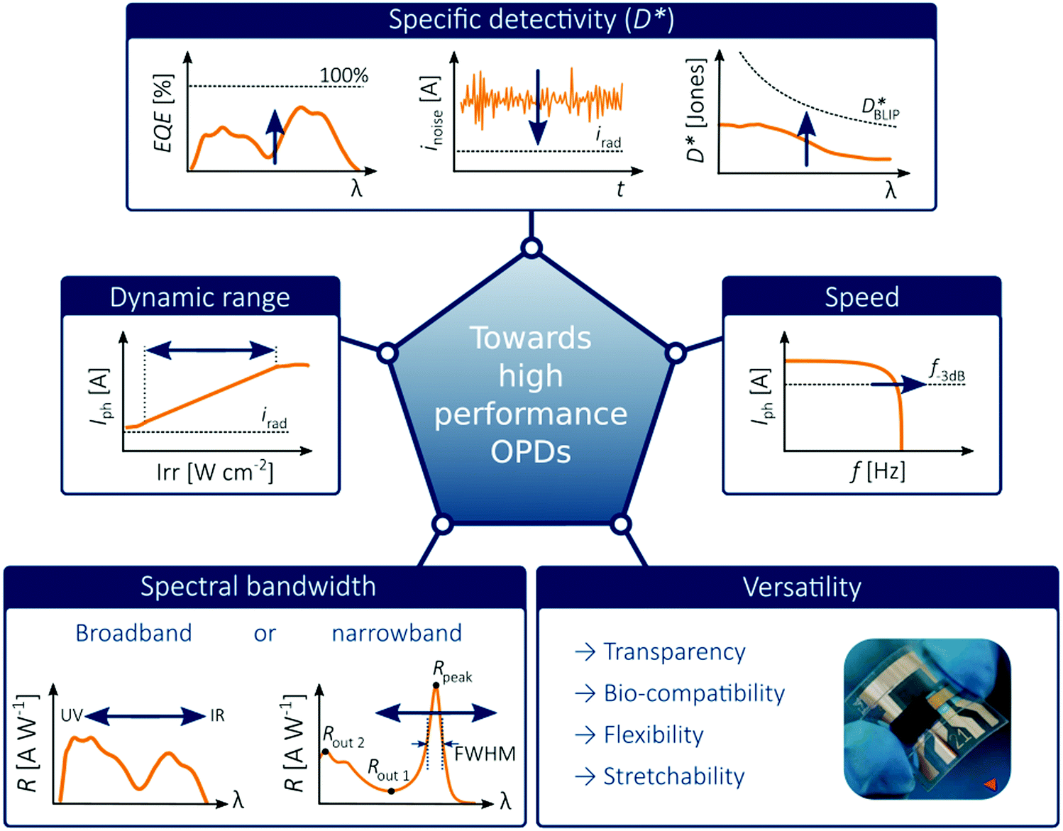 | ||
| Fig. 2 Illustration of challenges for emerging OPDs. The picture of the flexible OPD is reproduced with permission,27 copyright 2017, Springer Nature. | ||
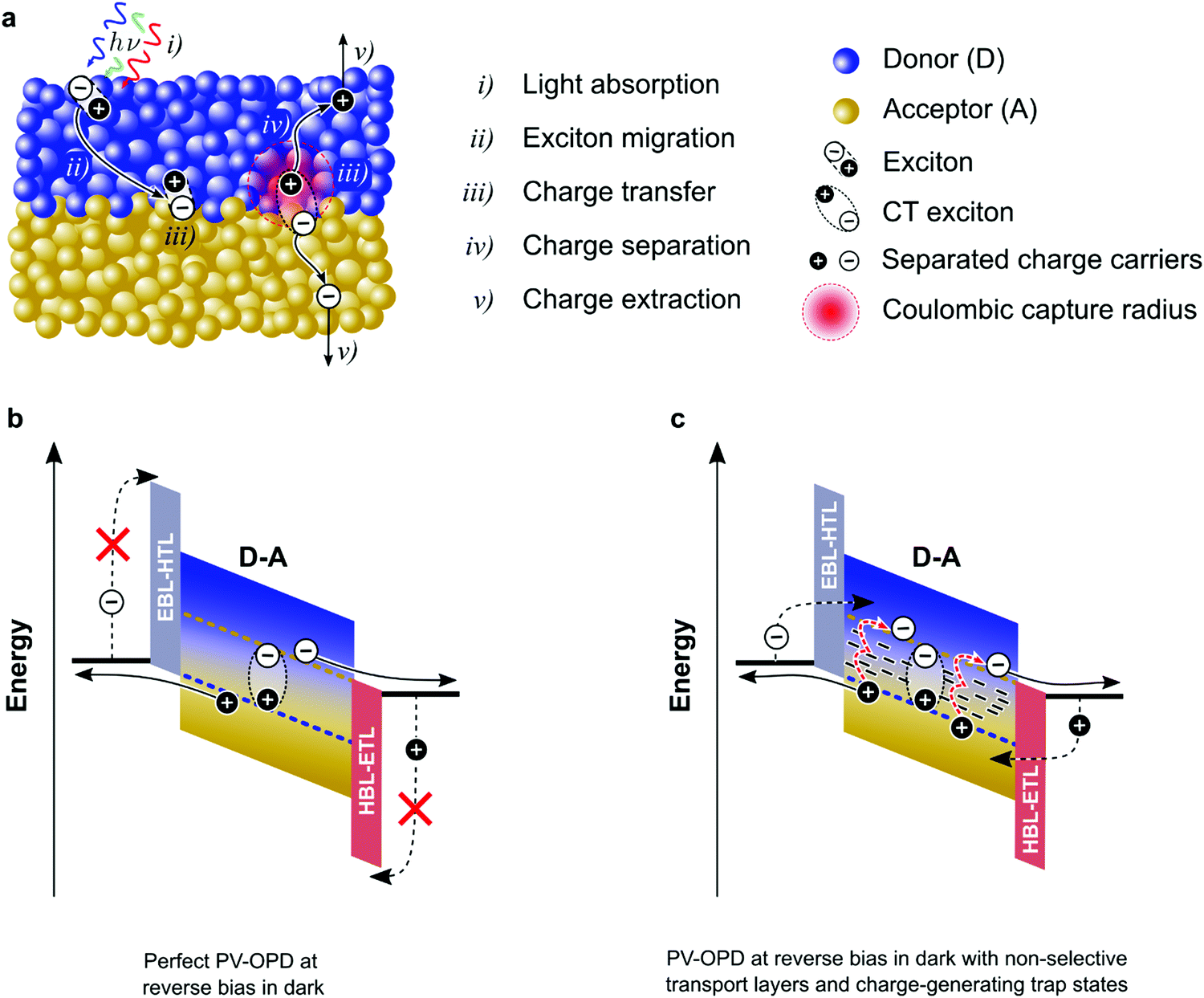 | ||
| Fig. 3 Processes involved in photo and dark current generation. (a) Representation of a D–A layer demonstrating the steps from light absorption (i) to charge extraction (v). For simplicity, light absorption is represented only in the donor phase, while in fact the acceptor and CT states can also absorb light and follow the same steps. (b) Energetic sketch of a perfect PV-OPD at reverse bias where JD is determined by J0 due to the thermal generation of charge carriers over CT states. (c) Non-ideal OPD at reverse bias showing different sources of JD, in addition to the ideal J0: injection from the contacts as a result of poor or absent blocking layers and generation via trap states (shallow or deep). | ||
High responsivity
For high responsivity (R), several optoelectronic processes must be optimized. These processes are summarized in Fig. 3a. A discussion about their state-of-art is given in the below.Most recently introduced materials, including NFAs with strong absorption as compared to fullerenes, were designed to target the absorption of the solar spectrum. This reduces the amount of D–A systems to be employed beyond 1000 nm, and compromises the development of NIR and IR OPDs.65,85 Additionally, OPDs generally contain transporting layers, which, as depicted in Fig. 3b and c, serve as selective and ohmic contacts. However, transporting layers also absorb light86 but do not generate charge carriers, being therefore a source of photon losses.87 Another source of losses refers to the Fresnel reflection at the semi-transparent electrode. Moreover, to achieve efficient charge dissociation, devices comprise nano-scale thin layers, which might not absorb the entire incoming radiation. Both issues have been addressed by optical manipulation such as light trapping.88,89 Optical manipulation has also been used to increase the absorption in the CT state spectral region; using optical microcavities, CT-OPDs have been demonstrated, where not only the absorption is enhanced but also narrowband photoresponse is achieved.27,74
Generally, exciton migration is described by two types of energy transfer process: the Förster96 and the Dexter97 energy transfer. In the former, also called Förster resonance energy transfer (FRET), energy is transferred by the dipole–dipole coupling between the donating and the accepting molecule. The efficiency of this transfer decreases with increasing distance between molecules as r−6, leading to a substantial contribution of FRET only within a D–A separation range of 1–5 nm.98,99 Note that here D and A refer to molecules of same species. As a rule of thumb, the FRET process dominates the singlet-exciton diffusion, while the diffusion of triplet-exciton between non-phosphorescent molecules is restricted to Dexter energy transfer type.67 The latter is a short-range interaction which depends on the overlap of the wave-function of donor and acceptor molecule and involves the physical exchange of an electron.
Assuming FRET as the main diffusion mechanism, LD depends on:
(a) the dipole–dipole orientation
(b) the intermolecular distance
(c) the photoluminescence (PL) quantum yield
(d) the spectral overlap between the PL of the donor and absorption of the acceptor
(e) the refractive index and
(f) the ratio τf/τ0, where τf is the PL lifetime limited by quenching defects and τ0 is the intrinsic PL lifetime in the absence of defects.100
Besides being difficult to control, both (a) and (b) have a minor impact on the final LD. Diminishing the non-radiative decay paths to increase the PL quantum yield (c) is expected to have a stronger influence on LD. Highly ordered crystals are also expected to improve LD. Lunt et al. showed that LD increases from 6.5 nm in the amorphous film to 25 nm in single crystals, which is also connected to changes in the PL quantum yield.101 Menke et al. showed that LD increases by diluting the donor into a matrix consisting of a high-gap material, leading to decreased non-radiative decay rates.93,102 By adding chemical side-groups to organic molecules, Raisys et al. increased the spectral overlap (d), thereby increasing LD. Moreover, a lower refractive index (e) should lead to a larger LD. Similarly to many properties of optoelectronic devices, traps (f) are detrimental for LD. Indeed, Monte Carlo simulations indicate that traps are responsible for a major reduction of LD.103 A detailed discussion on exciton diffusion in organic solids can be found in ref. 67 and 93.
According to Marcus theory, the electron transfer becomes more efficient as ECT becomes lower than the optical gap of the D–A system.105,106 In general, when using fullerenes as A, it is assumed that a driving force of about 0.1 eV is needed to assist efficient charge transfer,107–109 while recently reported NFA systems show desirable performance at negligible driving force.110,111 Nevertheless, as the energy offset Eopt–ECT decreases, repopulation of the singlet states becomes more probable, whose decay rates are faster than those of the CT states, being therefore associated with reduced device performance.112–115 In addition, some studies also suggest that if the triplet state on the D or A phase has a lower energy than ECT, it can be an efficient path for recombination.116 However, a further study indicates that fullerene triplets are responsible for recombination, whereas the D triplet states are inactive even though their energy is 300 meV lower than ECT.117 Moreover, it has been shown that triplets are not an active recombination path for non-geminate recombination.118
Another important discussion regarding CT states is which factors are decisive for efficient charge separation, see step (iv) in Fig. 3a. Because CT states are strongly bound,119 overcoming the Coulomb energy barrier is necessary to release free carriers. At room temperature, thermal energy is not sufficient to assist this transition and the question about how bound CT states get split arises. It has been proposed that higher-energy CT states are responsible for efficient free charge generation, while the yield provided by the relaxed ones would be low. The role of the so-called “hot CTs” has been intensively debated and a final conclusion is yet lacking. From a generation yield close to 100%, it has been shown that regardless of the excitation energy, IQE remains constant, down to photonenergies of ECT.120 Moreover, several groups have shown similar results from different perspectives, where no effects of the energy excess has been observed. However, different conclusions arise when considering ultrafast spectroscopy results.121 Experimental data suggests that higher-energy CT states are faster in generating free charges. In one study, an increase in photocurrent was observed when additional infrared pulses were applied to steady-state illumination.122 While experimental and theoretical studies point to the effect of higher-energy CT states,123 data obtained by other groups contradict those findings.124
Low dark current
The lower limit of JD in any PV-OPD is determined by the dark saturation current, J0, in addition to the diffusion current.37J0 arises from thermal generation of charge carriers over the states at which thermal equilibrium is achieved and is, therefore, unavoidable. For inorganic semiconductors, such states define the band gap, usually leading to low intrinsic dark currents. For organic semiconductors, however, the charge generation within single materials is rather poor, which was circumvented by the introduction of HJs formed between D and A. The charge-carrier generation happens at intermolecular CT states, whose energy ECT is lower than the optical gap of the single materials. In dark at zero bias, equilibrium between thermal generation and recombination is achieved via CT states. As sketched in Fig. 3b, when a negative bias is applied, thermally generated charges are extracted, causing J0 to be determined by the CT states properties:132,133
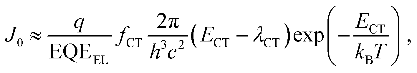 | (1) |
 | (2) |
In the field of OSCs, one of the recently broadly discussed topics is the origin of non-radiative voltage losses, which are much higher than in inorganic solar cells, and hence, limit the maximum achievable power conversion efficiency.135,139 It is worth noting that this discussion is also valid for OPDs, where non-radiative losses lead to higher J0 as predicted by a lower EQEEL in eqn (1). While the majority of the OPDs are still far above the non-radiative limit, in NIR absorbing devices non-radiative paths tend to become the major source of dark current.138 Different strategies have been reported for the reduction of extrinsic dark currents and are summarized below.
Aiming to increase the injection barrier at reverse bias meanwhile forming ohmic contact at forward bias, it is common to use layers that re-define the Fermi alignment of the contact. The most known material system for solution-processed devices is PEDOT:PSS for hole injection.145 For electron injection, different materials are employed, such as PEIE146,147 and ZnO nanoparticles.148 In vacuum-processed devices, ohmic contacts are generally achieved by molecular doping of electron-transporting layers (ETL) and hole-transporting layers (HTL),86 which also work as blocking layers in reverse bias for the opposite charge carrier type. While employing doped layers is a reliable solution to achieve selective contacts, it has been shown that lateral leakage currents arise from these layers, requiring device engineering to minimize this problem.149
Another issue is related to the roughness of the rather omnipresent ITO transparent contact. Spikes much higher than the average thickness of the layer resulting from patterning methods can lead to ohmic shunt paths, increasing JD. The problem can be circumvented by utilizing smoothing polymeric layers or increasing the thickness of the active layer.74,150–152
Intra-gap trap states are generally detrimental for the operation of optoelectronic devices. Besides the known effects on charge carrier mobility, increased recombination rates, and reduced LD, an increase of JD has also been attributed to traps, see Fig. 3c. Dark and photocurrent of OSCs were described according to the model proposed by Hurkx et al. for inorganic semiconductors,153,154 where the generation rate is increased by the tunneling of trapped charge carriers into the band. The model is a modified version of the Shockley-Read-Hall (SRH) theory. Assuming a Gaussian distribution of deep traps and SRH generation rates, Fallahpour et al. modeled the dark current of OPDs for the P3HT:PC61BM blend, even though the field dependence was not studied. The authors also discussed that injection from the contacts cannot explain the high JD.155 Recently, Kublitski et al. showed that JD is proportional to the experimentally measured amount of mid-gap traps and their characteristics. In the same work, JD was described by a field-assisted de-trapping model based on Poole–Frenkel effect, which explains the magnitude and field dependence of the experimental results.136 Moreover, the presence of mid-gap states was suggested to increase J0, re-defining the thermodynamic limit of organic solar cells and OPDs.156
Nonetheless, Simone et al. attributed the high JD and its activation energy to the injection of charge carriers from the contacts into the band tails of different polymers.157 Similarly, Zarrabi et al. suggested that band tails are the source of JD due to thermal generation over the reduced tail-to-tail optical gap.156 A better understanding of the extrinsic dark currents and their reduction will remain a key subject of research in the coming years.
Speed
The response speed of PV-OPDs can be limited by the RC time of the measurement setup (sheet resistance of the device, contact resistance and load resistance of the equipment), by the transit time of the slowest carrier or both as described by eqn (19).158 Therefore, strategies to increase the response speed in this class of devices target one or both of the limiting cases. On the one hand, reduced RC time can be achieved by employing smaller devices with reduced sheet resistance and, ideally, thick undoped layers. On the other hand, increasing the device thickness leads to an increased transit time τtr, which is undesired. τtr is determined mainly by the charge carrier mobility, therefore, the same trade-offs apply as discussed for charge collection.Saggar et al. showed that the response speed of PTNT:PC71BM (50 wt%) is limited by the slow electron transport as compared to the hole transport.159 By increasing the PC71BM concentration, the electron mobility was increased and the hole mobility slightly decreased. The balanced charge carrier mobilities led to an increase in the cutoff frequency, as shown in Fig. 4a. In the same direction of intentionally tuning transport properties, Ullbrich et al. fabricated devices comprising varying active areas, in order to study the intrinsic response speed (not RC limited) of narrowband CT-OPDs.160 The authors observed an increasing response speed upon decreasing active area due to the reduced capacitance (RC limit). The response speed saturates at 8 ns (0.07 nF), where the low hole mobility of the ZnPc donor limits the response speed. By engineering a planar-mixed (D/D–A/A) structure, the authors controlled the transit path for holes and electrons while keeping the device and active layer (D–A) thickness constant (see Fig. 4b). This approach led to a record cutoff frequency of 68 MHz as depicted in Fig. 4c.
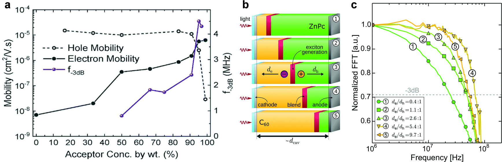 | ||
| Fig. 4 (a) PTNT:PC71BM blend-ratio impacts electron and hole mobilities along with the f−3dB of OPDs. The balanced charge mobility occurs at the PC71BM concentration of ∼95%, for which the largest f–3dB values (4.5 MHz) is achieved. (b) Simplified device architectures of the planar-mixed heterojunction cavity enhanced OPDs. Neat layers of ZnPc (donor) and C60 (acceptor) are depicted in green and orange, respectively. Excitons are generated and dissociated into free charge carriers at the interface colored in red. (c) Modulated frequency response of OPDs sketched in (b). With shortening the slower carrier (hole) travel distance by reducing the thickness of ZnPc layer, the cutoff frequency rises (① → ④) to the maximum value of 68 MHz. Panel (a) is reproduced with permission.159 Copyright 2021, Wiley-VCH GmbH. Panel (b) and (c) are reproduced with permission.160 Copyright 2017, American Chemical Society. | ||
In PM-OPDs, the response speed depends on the lifetime of trapped charges. Therefore, these devices are usually slower than PV-OPDs.36,161 The fastest PM-OPDs operate in the range of kHz,49 in contrast to the MHz range achieved by PV-OPDs. The response speed of PM-OPDs has been shown to increase with the applied voltage, which was attributed to a faster trap filling at the organic/metal interface.162 Likewise, employing organic crystals leads to a fast accumulation, increasing the response speed,163 which is also observed when a high negative bias is applied to devices comprising amorphous layers.59 An intuitive overview on the response speed of PM-OPDs is given in ref. 161.
Dynamic range
A large DR is required to precisely detect signal of various intensities. Whether the device operates in the linear or sublinear regime depends on the photophysics of charge carrier dynamics in the device. For PV-OPDs, non-linear photoresponse is generally observed at high light intensities, which is mostly attributed to non-geminate, bimolecular recombination.164 At high light intensities, a large amount of charge carriers accumulates at the D–A interfaces, increasing the probability of recombination and resulting in a reduced diffusion current. This effect becomes more pronounced if thick layers with low charge carrier mobility are involved.165 Poor extraction was further correlated with increased bimolecular recombination.166 In fact, it was shown that both non- and geminate recombination can be suppressed in devices with optimized morphology, which leads to an enhanced and field independent extraction.167,168Nonetheless, recent theoretical simulation by Hartnagel et al. predicted that recombination via trap states as well as spatial charge effects in thick devices can also lead to sublinear photoresponse at high light intensities. In the same study, the authors suggested that sublinear deviations at low light intensities are caused by exponential band tails.169
Further challenges
Narrowband OPDs
Traditional approaches for narrowband detection
Since decades, broadband inorganic PDs are state-of-the-art and different semiconductors cover a very broad range of the electromagnetic spectrum and achieve high D*. Nevertheless, it has been challenging to achieve monolithic, narrowband inorganic PDs and therefore other approaches have been chosen to realize color-discrimination for broadband detectors.Optical filters such as shortpass, longpass, and bandpass filters can be utilized to restrict the photoresponsivity of PDs such that only the intended wavelength range is detected. Such concepts are applied in CMOS- or CCD-based cameras where the color discrimination into the three primary colors is achieved usually by filters, utilizing the same semiconducting material for absorbing different colors. These detector-arrays are nowadays highly integrated and miniaturized, but still expensive. Additionally, the color selectivity is quite limited and different approaches are needed to achieve a spectroscopic resolution. Finally, the use of filters obviously generates losses.
For higher wavelength-resolution, typically, optically dispersive elements such as gratings (diffraction on a grating) or prisms (refraction in dispersive materials) are utilized to spatially decompose colors. Subsequently, the dispersed light is either detected by a line-detector, comprised by many individual PDs, or by selecting the relevant wavelength via an aperture such as slits in monochromator setups combined with a single broadband PD. In the latter configuration, the dispersive element is typically rotated to change the desired wavelength. Both of these approaches are highly performant and are the basis for scientific spectroscopy. Nevertheless, some of the intrinsic properties of the used components make such sensor systems rather large and expensive. For accurate detection of the separated wavelengths, the calibration of the dispersive elements is essential which is sensitive to environmental changes (e.g. temperature, vibrations). Additionally, line detectors are expensive, have limited lateral resolution and are sensitive to higher diffraction order of grating, restricting the detection range. All of these reasons lead to the fact that spectrometers are still quite expensive and, due to their fragile properties, mainly employed in laboratory environments.
Narrowband absorber materials
The spectral response of OPDs is correlated to the photo-absorbing layer (typically a D–A HJ), whose materials can be commonly classified into polymers and small molecules. By tailoring the molecular electronic structure, the absorption of new absorber materials can be sharpened for achieving narrowband OPDs. Both D and A materials have intrinsic photo-absorbing properties, which induce a broadened absorption of PHJ or BHJ systems. Hence, further strategies need to be employed to suppress the broad absorption. Emerging single-component systems have found to be promising in this regard. As shown in Table 1, PSQ19 and ISQ20 are a donor–acceptor–donor (D–A–D) single-component systems with a FWHM down to 110 nm and 80 nm and competitive D* up to 7.7 × 10¹² and 3.2 × 10¹² Jones, respectively. In Table 1, figures-of-merit and recent years progress of narrowband OPDs with employing narrow-photo-absorbing materials are summarized. The normalized EQE of some OPDs based on typical narrow bandgap absorbers are shown in Fig. 5. It is notable that narrowband OPDs are still suffering from lack of narrow-photo-absorbing materials with small optical gaps.175,176 Moreover, within this strategy, it is difficult to avoid a photoresponse outside the targeted detection window induced by the intrinsic absorption of photo-absorbing materials. In recent years, several advanced strategies were presented to realize narrowband OPDs, apart from chemical engineering of the absorber layer, which are presented below.| Photo-absorbing materials | Peak [nm] | FWHM [nm] | D* [Jones] | EQE [%] | R [A W−1] | Bias [V] | LDR [dB] | f −3dB [kHz] | Year | Ref. |
|---|---|---|---|---|---|---|---|---|---|---|
| Solution processing | ||||||||||
| 3:PC61BM | 500 | 130 | — | 8.2 | 0.03 | −1.0 | — | — | 2013 | 178 |
| 2:PC61BM | 525 | 80 | 1.00 × 10¹¹ | 15.0 | 0.06 | −1.0 | 80 | 25.0 | 2014 | 21 |
| Cy7-T:C60 | 850 | 100 | 1.00 × 10¹² | 17.0 | 0.12 | −1.0 | — | — | 2015 | 22 |
| 1(Pyrl):C60 | 481 | 76 | 2.00 × 10¹¹ | 18.0 | 0.07 | 0 | — | — | 2019 | 177 |
| PolyTPD:SBDTIC | 740 | 141 | 1.42 × 10¹³ | 10.5 | 0.06 | 0 | 78 | 118.0 | 2019 | 179 |
| PCZ-Th-DPP | 709 | 170 | 4.63 × 10¹² | — | — | −1.0 | 109 | 1.2 | 2019 | 180 |
| PCbisDPP:PC61BM | 730 | 210 | 4.73 × 10¹¹ | 80.0 | 0.31 | −3.0 | — | — | 2019 | 181 |
| PCPDTBT:ZnO | 725 | 175 | — | 68.0 | 0.40 | — | — | — | 2020 | 182 |
| PSBOTz:PNDBO | 530 | 155 | 1.10 × 10¹³ | 16.4 | 0.07 | −2.0 | — | — | 2020 | 183 |
| 1(Pyrl):1(Hex):C60 | 754 | 11 | 1.10 × 10¹⁰ | 14 | 0.086 | 0 | 61 | 150.0 | 2021 | 184 |
| Vacuum processing | ||||||||||
| DMQA:SubPc | 586 | 131 | 2.34 × 10¹² | 60.1 | 0.27 | −5.0 | — | — | 2013 | 185 |
| SubNc | 690 | 180 | — | 80.0 | 0.45 | −15.0 | — | — | 2015 | 186 |
| DM-2,9-DMQA:SubPc | 580 | 115 | 2.03 × 10¹² | 56.5 | 0.26 | −3.0 | — | 76.7 | 2014 | 187 |
| ISQ | 680 | 80 | 3.2 × 10¹² | 15.0 | — | −2.0 | 114 | 190.0 | 2016 | 20 |
| Rubrene:C60 | 470 | 80 | — | 55.0 | 0.21 | −1.0 | — | 86.0 | 2016 | 188 |
| M1:C60 | 550 | 67 | 3.73 × 10¹³ | 59.0 | 0.26 | −3.0 | — | — | 2016 | 72 |
| PSQ | 600 | 110 | 7.70 × 10¹² | 66.0 | 0.32 | −2.5 | 96 | — | 2017 | 19 |
| CiInPc:C60 | 705 | 190 | 3.30 × 10¹² | 80.0 | 0.45 | −1.0 | 77 | 2.9 | 2019 | 189 |
| 1a:C60 | 560 | 97 | 4.37 × 10¹³ | 70.0 | 0.32 | −3.0 | — | — | 2019 | 190 |
| SubPc:C60 | 600 | 70 | 7.50 × 10¹¹ | 16.0 | 0.08 | −1.0 | — | — | 2021 | 191 |
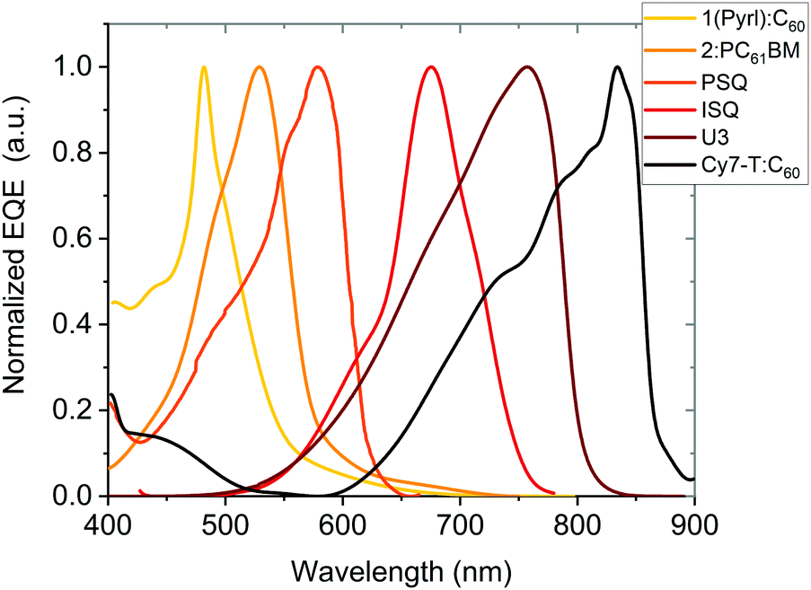 | ||
| Fig. 5 Normalized EQE of OPDs based on narrow-photo-absorbing materials as a function of wavelength. 1(Pyrl):C60177 and Cy7-T:C6022 are PHJs. 2:PC61BM21 is a BHJ blend. PSQ19 and ISQ20 are single-component photo-absorbing materials with D–A–D chemical structure and U3 is also single component device.23 | ||
Charge collection narrowing (CCN)
Armin et al. introduced an interesting concept to achieve narrowband detection by manipulating charge collection efficiency in devices comprising thick active layers.24 In this structure, incoming photons with energy above the optical gap (case A and B in Fig. 6a) are absorbed close to the transparent electrode. Holes photogenerated close to the anode (ITO) have a shorter transit time than that of photogenerated electrons, which must cross the entire thick layer. Hence, a space charge region arises, which screens the electric field responsible for the extraction, hindering charge collection. Therefore, electrons and holes in this region recombine. Incoming photons with energy near or slightly lower than the optical gap (case C in Fig. 6a), penetrate the device, reaching the back reflecting electrode. These photons create an interference effect such that generation happens in the entire bulk. In the ideal case, no space charge region is formed and both charge carrier types are efficiently extracted. In the photoresponse spectra, the balanced extraction is translated as a peak located at the absorption onset of the active layer. By varying the active layer thickness, one can tune the position of the peak, as shown in Fig. 6b. The authors were able to apply the CCN concept to two material systems, PCDTBT:PC71BM and DPP-DTT:PC71BM, leading to a NIR (shown in Fig. 6b) and red photoresponse, respectively. These devices reached D* on the order of 1011 Jones.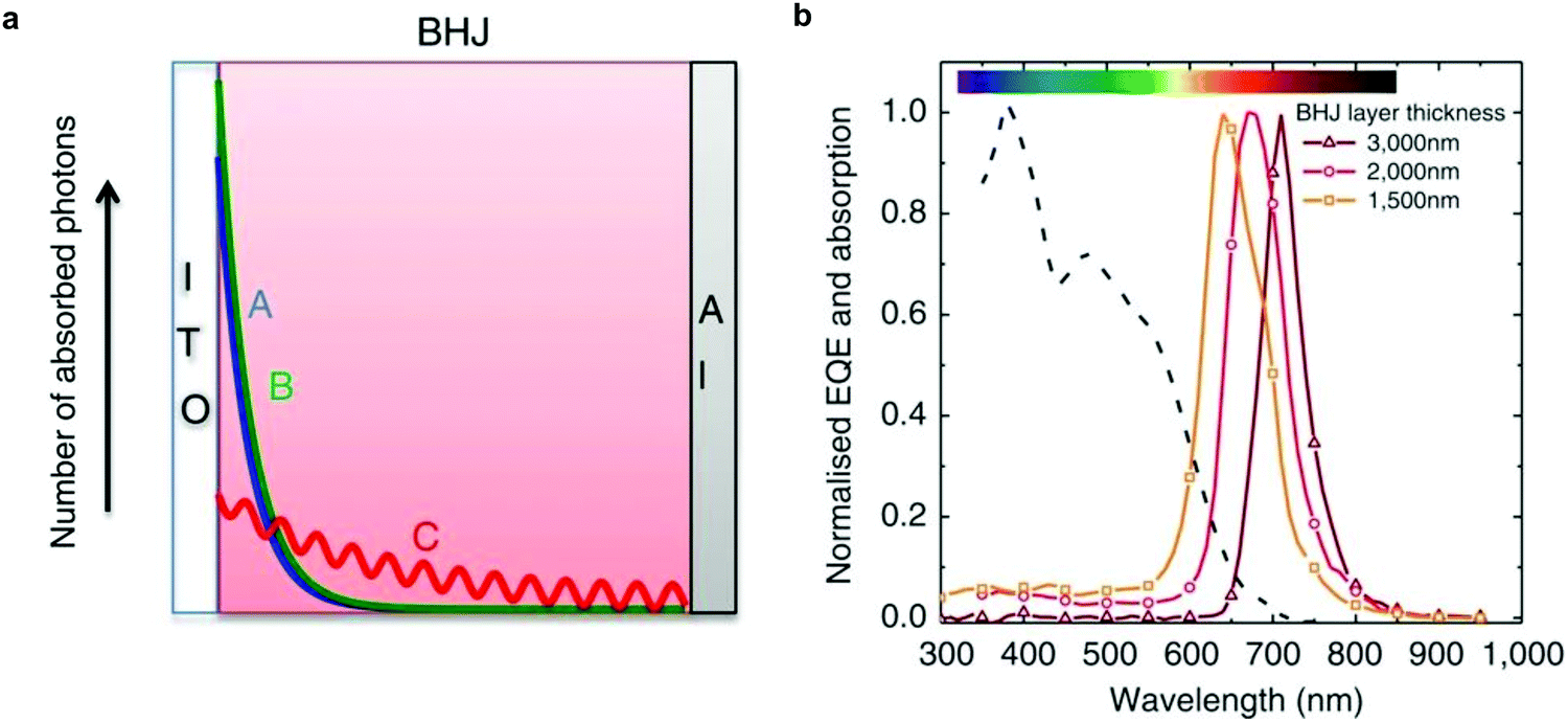 | ||
| Fig. 6 Working principle and narrowband response of CCN-OPDs. (a) The structure of the CCN-OPD is shown with the absorbed photon distribution for selected wavelengths (A–C). (b) Normalized EQE spectra of the CCN-OPD with three different active layer thicknesses. Reproduced with permission.24 Copyright 2015, Springer Nature. | ||
The disadvantage of this approach is that micrometer-thick devices are required, which should have an optical density αl ≫ 1 (assuming α ≈ 105 cm−1 for organic materials), where α and l are the absorption coefficient of the active layer and the device thickness, respectively. This issue was circumvented by the same group by using inverted devices comprising unbalanced mobilities.192 In this structure, only photons with energy close to the absorption onset generate holes that can be extracted, since they are close to the anode. Photons with energy above the optical gap generate slow holes close to the cathode. These holes cannot reach the anode and, therefore, recombine. With this approach, the thickness of the active layer was reduced to 700 nm, in contrast to the micrometer range previously required, and D* on the order of 1013 Jones was demonstrated at 700 nm response wavelength.192
Charge injection narrowing (CIN)
Charge injection narrowing (CIN) was introduced by Wang et al.25 and shares similarities with the concept of CCN discussed above. CIN combines the idea of CCN with photomultiplication, in order to achieve a narrowband spectral response with bias-enhanced EQE. The idea behind the spectral narrowing is the same; however, the active layer comprises a low-acceptor content, as previously reported for PM-OPDs.161 Therefore, electrons generated near the cathode by photons with energy close to the absorption onset of the D–A system accumulate due to the reduced percolation paths. The accumulation leads to an energy level bending under applied reverse bias, triggering enhanced hole injection caused only by spectrally selected wavelengths.The concept was also applied to achieve a dual band device which works as a conventional broadband PM-OPD when illuminated from the top and a narrowband CIN-PM-OPD when illuminated from the bottom, as shown in Fig. 7.193 Interestingly, since the interference depends on the reflection of the incoming photons, when illuminated from the bottom and operated as a CIN-PM-OPD, the devices become more efficient with increasing top electrode thickness. Oppositely, when illuminated from the top and operated as a conventional PM-OPD, devices become less efficient with increasing the top electrode thickness due to the reduced incoming light. Both operation regimes lead to D* in the range of 1011 Jones.
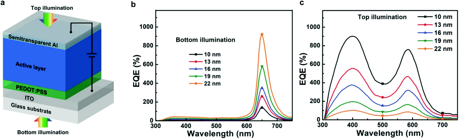 | ||
| Fig. 7 (a) CIN-PM-OPD structure. EQE of the CIN-PM-OPD under (b) bottom and (c) top illumination. Reproduced with permission.193 Copyright 2018, Wiley-VCH GmbH. | ||
Self-filtering narrowband OPDs
Self-filtering narrowband OPDs have been proposed as a promising strategy in recent years to achieve narrowband photodetection. The large binding energy and small diffusion length of photogenerated Frenkel excitons are viewed as a significant drawback of organic semiconductors. However, this property offers the potential to achieve self-filtering narrowband OPDs with the help of a hierarchical device structure where thick larger optical gap donor layers are followed by a lower optical gap acceptor layer. Excitons generated by high-energy photons in donor front layers fail to separate into free charges. Only low-energy photons with a long penetration depth can reach the D–A interface and generate free charges for collection. Compared to the CCN method, thinner devices can be realized with high response speed and simple fabrication methods.Xing et al. reported this device principle with a simple organic PHJ architecture that enables selective activation of excitons for tuning the photoresponse spectra.83 The schematic device structure is shown in Fig. 8a. By adjusting the ratio of PTB7 in P3HT, an improved responsivity and red-shifted photoresponse peak from 645 to 745 nm were demonstrated simultaneously (Fig. 8b). The truly filterless device exhibited D* above 1012 Jones with a narrow FWHM of around 50 nm. Concomitantly, Xie et al. proposed the same principle to manipulate the dissociation of Frenkel excitons intentionally.26 The basic device architecture and working mechanism are displayed in Fig. 8c. Due to the exciton dissociation narrowing, the filter-free narrowband OPD was accomplished, showing a peak EQE of around 65% at 860 nm with a FWHM of around 50 nm. Meanwhile, D* over 1013 Jones was demonstrated (Fig. 8d). This device was one the best performing gainless type narrowband OPDs ever reported, with performance comparable to commercial Si PDs. Similarly, Lan et al. fabricated narrowband OPDs with a heterostructured photoactive layer comprising a depletion layer and a BHJ layer (Fig. 8e).73 It was found that a 430 nm thick P3HT depletion layer combined with a 120 nm thick PBDB-T:m-ITIC BHJ absorbed the incident light for wavelengths smaller than 600 nm and gave a photoresponse in the deep-red region (Fig. 8f). Moreover, this work presented an inspiring option for application in de-multiplexing light communication.
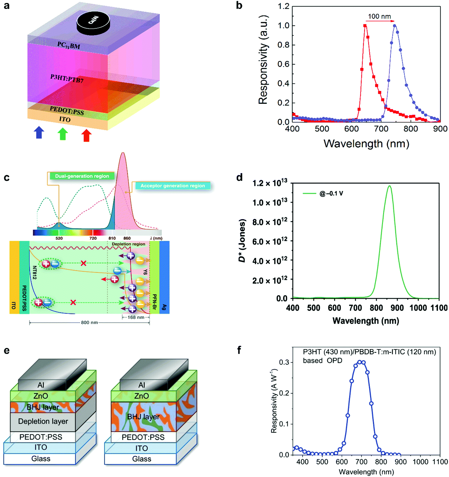 | ||
| Fig. 8 Working principle and the narrowband response of self-filtering OPDs. (a) Device structure and (b) the tunability of normalized response peak of red-light OPDs.83 (c) Working mechanism and (d) specific detectivity spectra (obtained from the dark current density) of self-filtering narrowband OPDs.26 (e) Device structures and (f) responsivity spectrum under zero bias for the filter-free band-selective OPDs. Panel (a) and (b) are reproduced with permission.83 Copyright 2020, American Chemical Society. Panel (c) and (d) are reproduced with permission.26 Copyright 2020, Nature Publishing Group. Panel (e) and (f) are reproduced with permission.73 Copyright 2020, Wiley-VCH GmbH. | ||
Microcavity enhanced narrowband OPDs
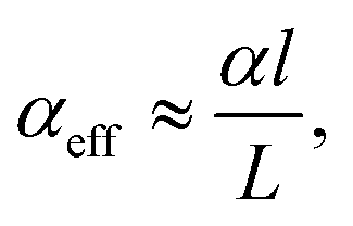
In the past years, Fabry–Pérot microcavity-based80 organic electronic devices have been demonstrated as a versatile methodology to realize narrowband OPDs with enhanced performance. Such resonance cavity enhanced OPDs are endowed with broad wavelength-range tunability and high selectivity. Moreover, the enhanced optical field within the cavity can also improve the total absorption of the photo-absorbing layer, resulting in enhanced spectral response at the resonance wavelength. Within the resonance cavity rejected wavelength range, the OPD has a much lower photoresponse than that of the resonance wavelength, leading to a high spectral rejection ratio (SRR), which indicates a good signal specificity. The tunability of the resonance wavelength can be easily realized by varying the thickness of layers within the cavity, allowing to build compact and highly integrated spectrometers without synthesizing new organic semiconductors for each wavelength.Physics of microcavities. In general, the intrinsic absorption coefficient (α) at peak wavelength of typical photo-absorbing materials is around 105 cm−1,82,85,194 which gives an absorption attenuation length of around 50 nm. Therefore, in normal organic electronic devices, such as OSCs, the needed photo-absorbing layer thicknesses are several tens to one hundred nanometers to achieve as high as possible absorption. In a cavity enhanced narrowband OPD, the effective absorption coefficient αeff can be approximated by eqn (3). Compared to the photo-absorbing material, the absorption coefficient of interlayers and reflecting electrodes are neglected for this approximation.
 | (3) |
 | (4) |
 | (5) |
Utilizing above-gap absorption. To achieve OPDs with a small FWHM by employing photo-absorbing materials that are normally designed with high intrinsic α, the thickness of the photo-absorbing layer needs to be much thinner as compared to OSCs. Wang et al. fabricated cavity enhanced OPDs with a photo-absorbing layer thickness in the nanometer scale.81 As shown in Fig. 9, tunable narrowband OPDs with a detection window covering the visible wavelength range were realized by using only 3 and 6 nm thick photo-absorbing layers. The resonance wavelength was tuned by varying the thickness of the microcavity, realized by varying the thickness of ETL and HTL simultaneously to ensure that the photo-absorbing layer is located in the optimized electromagnetic field, at which the cavity enhancement reaches the highest value. In Fig. 9b, the FWHM values of the OPDs were ranging between 28 and 43 nm in second order resonance (m = 2). By increasing the cavity thickness, the third order resonance (m = 3) was achieved, decreasing the FWHM to 25 nm with a resonance wavelength peak at 630 nm and 25% EQE. Even if the thickness of the photo-absorbing layer was only a few nanometers, the OPDs achieved a shunt resistance as high as 1 MΩ cm2, leading to a specific detectivity over 1012 Jones.
 | ||
| Fig. 9 EQE curves and correlated FWHM of cavity enhanced OPDs with (a) 3 nm thick photo-absorbing layer and third order resonance (m = 3) and (b) 6 nm thick photo-absorbing layer and second order resonance (m = 2). The tunable enhanced wavelengths are realized by varying the thickness of ETL and HTL. Reproduced with permission.81 Copyright 2019, American Chemical Society. | ||
Utilizing intermolecular CT state absorption. Dramatic efforts have been performed to synthesize organic semiconductor materials with narrow optical gap to extend the OPDs detection wavelength range into the NIR.22,184 New materials rarely give a reasonable photoresponse beyond 1100 nm.4,16,195 Additionally, it is challenging to achieve high detectivity in the NIR range by employing a materials with a narrow optical gap, which suffer from high noise current at zero external bias.37,196 In 2017, Siegmund et al. introduced a promising method to achieve narrowband NIR OPDs by inserting a D–A BHJ inside a microcavity (Fig. 10a), utilizing thermal evaporation.27 With blending D and A materials, intermolecular CT states are formed, featuring optical transitions below the D and A optical gaps (Fig. 10b). In general, the absorption coefficient of CT states is less than 103 cm−1 and continually declines with increasing wavelength. Therefore, the photoresponse induced by CT absorption is rather weak. The cavity enhances the absorption caused by intramolecular CT states and consequently a useful absorption well below the D and A optical gap is made possible. As shown in Fig. 10c, an EQE enhancement at CT absorption wavelength range up to 41-fold was achieved, with EQEs exceeding 20% and FWHM down to 36 nm. The narrowband NIR detection with wavelength tunability ranges from 810 nm to 1100 nm. Using an analogous strategy and employing a donor with a high HOMO level, D8, blended together with C60, Kaiser et al. realized cavity enhanced narrowband NIR OPDs based on CT absorption with tunability covering the NIR from 810 to 1665 nm, and achieving a D* at 1665 nm as high as 3 × 10⁸ Jones.197 Based on the work of Siegmund et al., Mischok et al. combined a highly reflective distributed Bragg reflector (DBR) with a thin metal resulting in a sharp Tamm plasmon-polariton resonance. Compared with non-DBR devices, the performance of NIR OPDs based on CT absorption improved impressively, showing enhanced EQE up to 17% at a wavelength of 880 nm with FWHM down to 20 nm.198
 | ||
| Fig. 10 (a) Simplified device architecture of a microcavity enhanced narrowband NIR OPD. (b) Schematic energy level diagram of the main materials involved in the OPDs. (c) NIR OPDs based on ZnPc:C60 CT state absorption. (d) NIR OPDs based on the CT absorption of D8:C60. Subfigures (a–c) are reproduced with permission.27 Copyright 2017, Springer Nature. Subfigure (d) is reproduced with permission.197 Copyright 2019, American Chemical Society. | ||
Later on, the group also realized microcavity enhanced CT absorption narrowband NIR OPDs by solution processing.74 With varying the thickness of the active layer (PBTTT:PC61BM) from 290 nm to 440 nm, the second order resonance was achieved with EQE enhancement up to 40% at wavelength 720 nm (Fig. 11a) and FWHM (Fig. 11b) down to 20 nm at wavelength 910 nm. Benefiting from the thick active layer, the OPDs showed extraordinarily low dark current, resulting in D* up to 1013 Jones (Fig. 11c), which is comparable to state-of-the-art silicon PDs. To extend the response further into the NIR, the authors employed PDPPTDTPT:SdiCNPBI as active layer demonstrating narrowband OPDs operating at wavelengths up to 1700 nm. Furthermore, Tang et al. also integrated several of these CT-OPDs with varying active layer thickness on a single substrate and thereby realized a miniaturized spectrometer, see Fig. 19a. As a showcase, the transmittance spectrum of water was reproduced, detailed information is supplied in the section: Potential application of narrowband OPDs.74
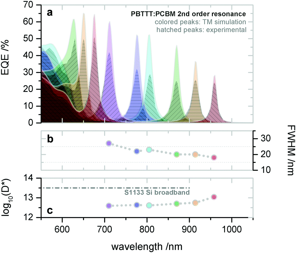 | ||
| Fig. 11 Solution processed PBTTT:PC61BM CT-OPDs based on the second order resonance. (a) Simulated and experimental (hatched) resonance wavelength and correlated EQE curves. The wavelength tunability in range of 650–910 nm was realized by varying the active layer thickness from 290–440 nm. (b) Corresponding FWHM and (c) D*. Reproduced with permission.74 Copyright 2017, WILEY-VCH GmbH. | ||
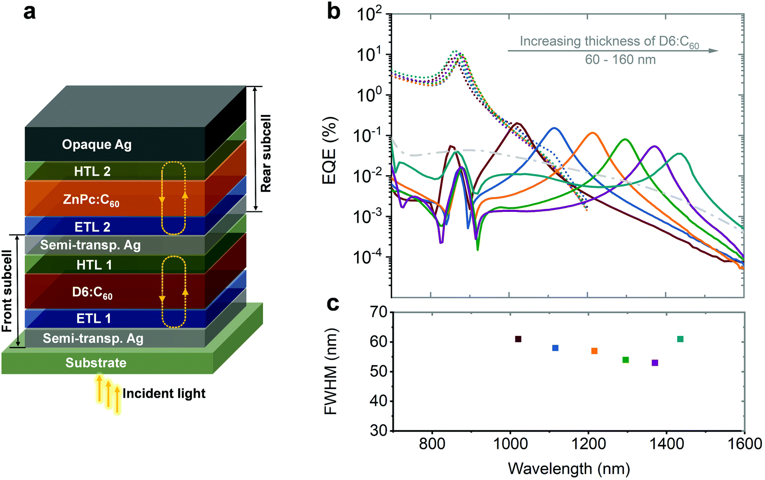 | ||
| Fig. 12 (a) Simplified device architecture of the microcavity enhanced stacked dual-wavelength narrowband NIR OPDs based on CT state absorption. (b) EQE curves and correlated FWHM of the NIR OPDs. The wavelength tunability was realized by varying the thickness of the photo-absorbing layer in one sub-cell while keeping the other constant. The thickness of D6:C60 was varied from 60 to 160 nm, resulting in a tunable wavelength covering the 1020–1435 nm range (solid lines). The EQE of the other subcell (ZnPc:C60) only changes negligibly (dashed lines). (c) The FWHM of each device are depicted in the lower panel. Licensed under CC BY 4.0.82 | ||
The tunability of each sub-cell was realized by varying the thickness of the photo-absorbing layer in one sub-cell, while keeping the other constant. As shown in Fig. 12b, the photo-responses of the thickness-varied sub-cell are tuned and those of the thickness-constant sub-cell remain constant (with negligible fluctuation). The tunable resonance wavelengths of the D6:C60 sub-cell were covering 1020–1435 nm (D6:C60 sub-cell). It is worth noting that the FWHM of the sub-cells was reduced to 61 nm. For the ZnPc:C60 sub-cell, a response wavelength of 790–1180 nm and an FWHM down to 35 nm could be achieved.82 As an application demonstration, the OPDs were utilized to determine ethanol concentration in a water solution by selecting a combination of two wavelengths corresponding to specific absorption bands from both liquids.
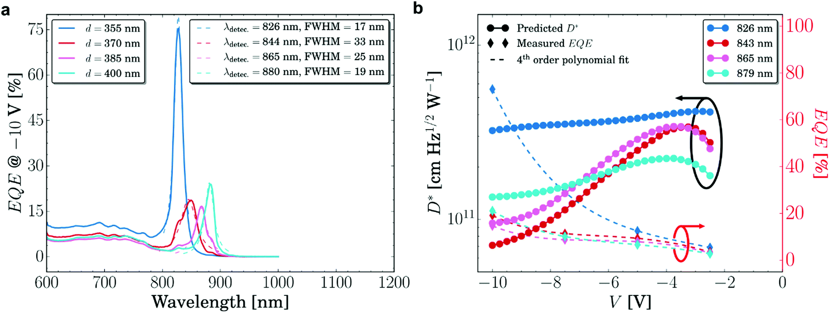 | ||
| Fig. 13 (a) Amplified EQE of narrowband CT-PM-OPD at four resonance wavelengths at −10 V. (b) EQE and D* of the same devices shown in (a) at various voltages.201 Licensed under CC BY 4.0. | ||
Combining microcavities with PM-OPDs represents a promising path to improve the sensitivity of CT-OPDs, since the benefits from the core properties of both devices can be combined. Nonetheless, narrowband PM-OPDs share the same drawbacks of PC-OPDs, which include generally higher JD and low response speed as compared to PV-OPDs. However, a clear understanding of these properties is still missing.
Challenges for narrowband detection
As described previously, to realize monolithic narrowband OPDs, many different methods have been utilized such as synthesizing materials with narrowband absorption19–21,23 and developing novel device architectures e.g. CCN,24 CIN,25 and self-filtering OPDs.26 However, by employing these methods, each material system can only supply one specific detection window, lacking an easy possibility for tuning the peak response wavelength. Furthermore, to manipulate the optical field distribution, a thick photo-absorbing layer or dissipation layer is always needed, which is feasible only with a few organic semiconductor materials and often brings processing difficulties.By employing microcavities, the OPDs’ response wavelength can be easily tuned in visible spectrum (400–700 nm)81 based on above-gap absorption and in NIR wavelength range (810–1665 nm)198 based on CT state absorption. However, by introducing microcavities, the photoresponse enhancement and selectivity are directly correlated to the optical interference, which is a double-edged sword, leading to the following drawbacks:
• The angular dependence of the photoresponse is an intrinsic property of cavity-based devices. Siegmund et al.27 and Wang et al.82 described this phenomenon and a 50 nm blue-shift of the resonance peak wavelength was observed with light incidence angles larger than ±45°. Within ±20°, the resonance did not shift more than 10 nm for a CT-OPD with the FWHM of 36 nm.27 For application, the light acceptance cone can be reduced (e.g. ±15°) to ensure the spectroscopic accuracy of the measured signal.82
• Control of higher order cavity resonances. As expressed in eqn (5), to achieve the tunability of response wavelength (λm), the microcavity thickness (L) needs to be varied, which can be realized by controlling the thickness of either transporting layer (ETL or HTL) or photo-absorbing layer in an OPD. A longer response wavelength requires a thicker cavity device. To realizing a wavelength tunability in range of 650–910 nm for second order resonance (m = 2), Tang et al. varied the photo-absorbing layer from 290 to 440 nm.74 Higher order resonances usually lead higher EQEs and narrower FWHM but thicker cavities are required, which in turn brings the issue of depositing thick organic layers.
• Signal from other absorption regions. To avoid unexpected response signals induced by higher order resonances at shorter wavelengths than the design-resonance or the intrinsic main absorption of involved photo-absorbing materials, a bandpass filter or a layer of intrinsic photo-absorbing material might need to be integrated in front of the OPDs, increasing the processing complexity.27
• Photo-absorbing material combination for multiple wavelength sensing. As shown in Fig. 12b, stacked, multi-wavelength sensing OPDs are suffering undesired resonance cross-talk due to coherent coupling of both sub-cavities. The phenomenon can be suppressed by careful selection of the photo-absorbing material system combination. The materials are supposed to have large difference of absorption coefficient in the targeted wavelength range. Transfer matrix modelling can assist the selection by simulating the optical field distribution within both microcavities.
In Fig. 14, the advantages and disadvantages of the presented approach to achieve narrowband photodetection in OPDs are summarized and are compared to the traditional approaches of applying inorganic broadband PDs in conjunction with either optical transmission filters or dispersive elements.
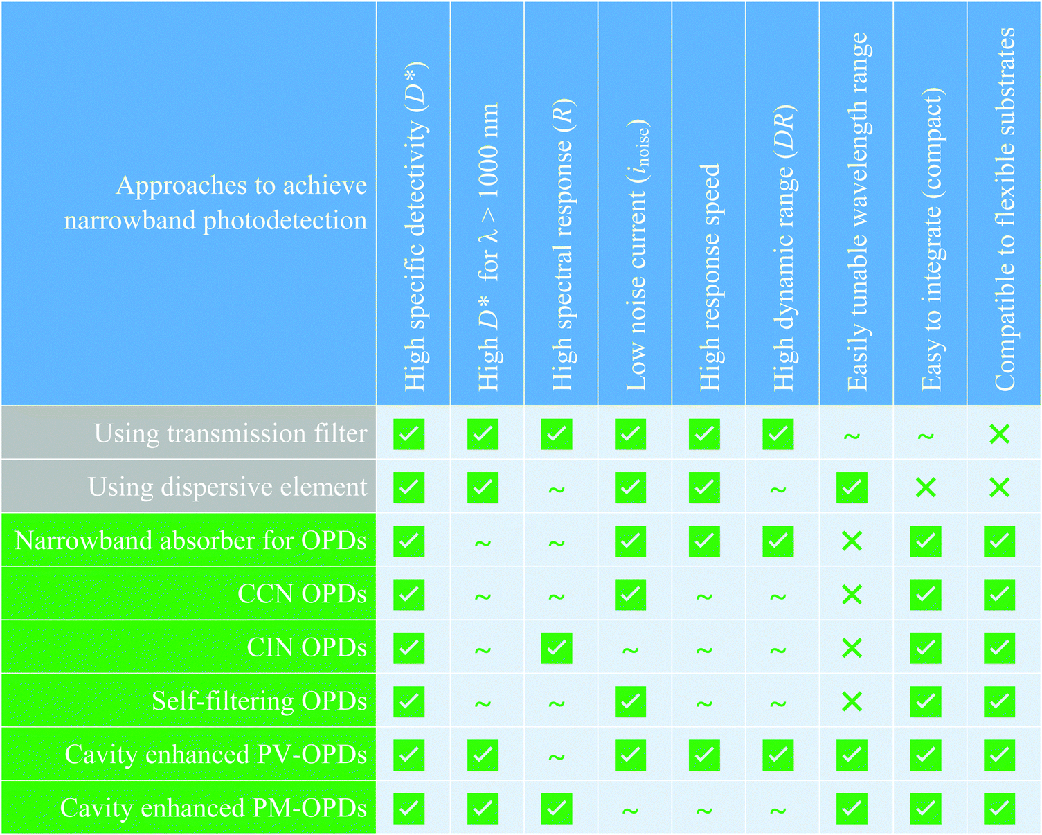 | ||
| Fig. 14 Comprehensive summary of advantages and disadvantages of all different approaches to achieve narrowband photodetection in this review. In grey, the traditional approaches using filter or dispersive elements are shown. In green approaches based on OPDs are highlighted. The checkmark, tilde, and cross indicate whether a specific approach can either succeed, maybe succeed, or falls short in a certain category, respectively. | ||
State-of-the-art performance of recent narrowband OPDs
Fig. 15 visualizes the recent performance status of OPDs based on D*, the most important performance metric of PDs, classified by fabricating methods (solution or vacuum processing) and spectral sensing bandwidth (broadband or narrowband). More information on the OPDs shown in Fig. 15 are summarized in Table 2, giving a detailed overview of the recent progress of state-of-the-art OPDs.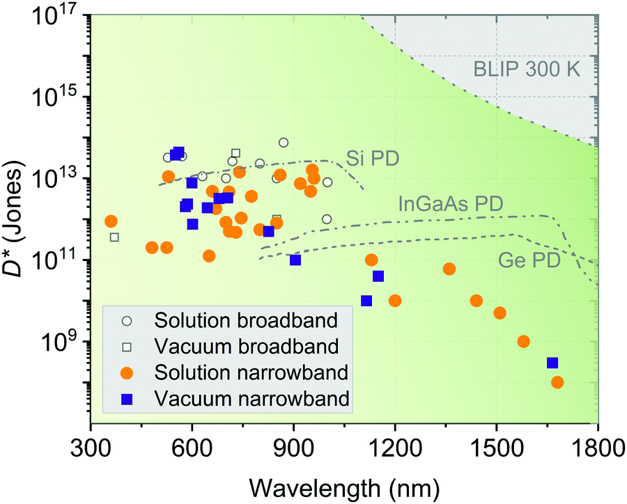 | ||
| Fig. 15 D* as a function of wavelength based on different device processing methods (solution vs. vacuum processing) and photodetecting wavelength bandwidths (broadband vs. narrowband detection). Further details about the individual devices are given in Table 2. The D* of Si, InGaAs and germanium (Ge) are extracted from ref. 138. The BLIP limit is calculated at 300 K for photovoltaic PDs with a field-of-view of 2π. | ||
| Photo-absorbing materials | Type | Target peak [nm] | Spectral range [nm] | FWHM [nm] | D* [Jones] | EQE [%] | R [A W−1] | Bias [V] | LDR [dB] | f −3dB [kHz] | Year | Ref. |
|---|---|---|---|---|---|---|---|---|---|---|---|---|
| a D* calculated at wavelength 566 nm. b D* calculated at bias voltage of −0.5 V. c The f−3dB measured at bias voltage of −5.0 V. d D* calculated at bias voltage of −0.5 V. e The f−3dB characterized at bias voltage of −1.0 V. f D* calculated at wavelength 1000 nm. g D* calculated without bias. h The Cy7-T and C60 were spin-coated and evaporated, respectively. i D* measured at −10 V bias. j D* measured at −10 V bias. k R measured at −10 V bias. l Incorrectly calculated by the authors. m The measured device had peak wavelength at 843 nm. | ||||||||||||
| Solution broadband | ||||||||||||
| PCDTBT:PC61BM | 528 | 300–800 | 3.2 × 10¹³![[thin space (1/6-em)]](https://www.rsc.org/images/entities/char_2009.gif) a a |
27.00 | 0.31 | −2.0 | 148 | 91.0 | 2016 | 146 | ||
| PCDTBT:PC71BM | 570 | 400–720 | 3.5 × 10¹³ | 76.00 | 0.35 | −5.0 | 100 | 50.0 | 2015 | 202 | ||
| PCDTBT:PC71BM | 532 | 300–800 | ∼1.0 × 10¹³b |
70.00 | 0.30 | −1.0 | 180 | 1000.0c | 2014 | 203 | ||
| PBDB-T:PbS-TBAI | 630 | 400–1000 | 1.1 × 10¹³ | 334.60 | 1.70 | −40.0 | 65 | — | 2018 | 204 | ||
| PBDTTT-C:PC71BD | 700 | 350–800 | ∼1.0 × 10¹³ | 30.00 | 0.17 | −2.0 | ∼140 | ∼20.0 | 2013 | 205 | ||
| NT40:N2200 | 720 | 300–850 | 2.6 × 10¹³ | 56.00 | 0.33 | −0.1 | 97 | ∼10.0 | 2019 | 206 | ||
| PDDTT:PC61BM | 800 | 300–1450 | 2.3 × 10¹³d |
25.00 | 0.16 | −0.5 | ∼100 | — | 2009 | 16 | ||
| PDPP3T:PC71BM | 850 | 300–1000 | ∼1.0 × 10¹³ | 28.00 | 0.19 | −0.5 | 148 | 400.0e | 2015 | 207 | ||
| CS-DP:PC71BM | 850 | 300–1000 | 8.0 × 10¹²f |
48.00 | 0.33 | 0 | — | — | 2018 | 208 | ||
| NT40:IEICO-4F | 870 | 300–1000 | 7.5 × 10¹³ | 57.20 | 0.40 | −0.1 | 123 | ∼100 | 2021 | 209 | ||
| Vacuum broadband | ||||||||||||
| C60 | 370 | 300–700 | 3.6 × 10¹¹ | ∼40.00 | 0.12 | −6.0 | 180 | 95.0 | 2013 | 210 | ||
| ClAlPc: C70 | 730 | 300–800 | 4.1 × 10¹³g |
74.60 | 0.44 | −2.0 | 173 | 778.7 | 2020 | 211 | ||
| Cy7-T:C60h | 850 | 600–870 | 1.0 × 10¹² | 23.00 | 0.17 | −2.0 | ∼100 | — | 2015 | 22 | ||
| Solution narrowband | ||||||||||||
| 1(Pyrl):C60 | NBM | 481 | 420–550 | 76 | 2.0 × 10¹¹ | 18.00 | 0.07 | 0 | — | — | 2019 | 177 |
| PCDTBT:PC71BM | CCN | 670 | 610–800 | 85 | 1.8 × 10¹² | 35.00 | 0.10 | −1.0 | 160 | 95.0 | 2015 | 24 |
| DPP-DTT:PC71BM | CCN | 950 | 900–1020 | 80 | 4.8 × 10¹² | 7.31 | 0.06 | −1.0 | — | — | 2015 | 24 |
| P3HT:PC61BM:CdTe | CCN | 660 | 650–850 | 100 | 4.8 × 10¹² | 200.00 | 1.06 | −6.0 | 220 | 900.0 | 2016 | 212 |
| P3HT:PC71BM | CIN | 650 | 640–700 | 28 | 1.4 × 10¹¹i |
53500.00 | 278.00 | −60.0 | 160 | — | 2017 | 25 |
| P3HT:PC71BM | CIN | 800 | 790–800 | 30 | 5.5 × 10¹¹j |
2000.00 | 0.85k | −50.0 | 170 | — | 2018 | 193 |
| P3HT:PTB7-Th:BEH | CIN | 850 | 830–880 | 27 | 8.0 × 10¹¹ | 15300.00 | 105.00l | −13.0 | 145 | — | 2021 | 213 |
| F8T2:ZnO | PM | 360 | 350–400 | 20 | 8.8 × 10¹¹ | 2170.00 | 6.5 | −15.0 | — | 0.1 | 2018 | 214 |
| PTB7:PC71BM | SF | 745 | 645–745 | 50 | 1.1 × 10¹² | 4.51 | 0.03 | 0 | 103 | 38.5 | 2020 | 83 |
| NT812:Y6 | SF | 860 | 860–960 | 50 | 1.2 × 10¹³ | 61.00 | 0.42 | −0.1 | — | — | 2020 | 26 |
| DT-PDPP2T-TT:Y6 | SF | 920 | 860–960 | 40 | 7.4 × 10¹² | — | — | −0.1 | — | — | 2020 | 26 |
| DT-PDPP2T-TT:Y6 | SF | 955 | 860–960 | 50 | 1.6 × 10¹³ | — | — | −0.1 | — | — | 2020 | 26 |
| PBDB-T:m-ITIC | SF | 700 | 750–950 | 120 | 8.3 × 10¹¹ | 53.00 | 0.30 | 0 | — | 80.0 | 2020 | 73 |
| PBTTT:PC61BM | MC | 775 | 700–1100 | 15 | 3.6 × 10¹² | 40.00 | 0.25 | 0 | 130 | — | 2017 | 74 |
| PBTTT:PC61BM | MC | 960 | 700–1100 | 17 | 1.0 × 10¹³ | 24.00 | 0.19 | 0 | 130 | — | 2017 | 74 |
| PDPPTDTPT:SdiCNPBI | MC | 1200 | 1000–1700 | 35 | 1.0 × 10¹⁰ | 0.90 | 0.01 | 0 | — | — | 2017 | 74 |
| PDPPTDTPT:SdiCNPBI | MC | 1440 | 1000–1700 | 38 | 1.0 × 10¹⁰ | 0.10 | 1.16 × 10 −3 | 0 | — | — | 2017 | 74 |
| PDPPTDTPT:SdiCNPBI | MC | 1580 | 1000–1700 | 47 | 1.0 × 10⁹ | 0.05 | 6.37 × 10 −4 | 0 | — | — | 2017 | 74 |
| PDPPTDTPT:SdiCNPBI | MC | 1680 | 1000–1700 | 41 | 1.0 × 10⁸ | 0.01 | 1.36 × 10 −4 | 0 | — | — | 2017 | 74 |
| PCDTPTSe:PC71BM | MC | 710 | 650–1510 | 60 | ∼5.0 × 10¹¹ | 18.00 | 0.10 | 0 | 146 | — | 2021 | 18 |
| PCDTPTSe:PC71BM | MC | 1130 | 650–1510 | 45 | ∼1.0 × 10¹¹ | 6 | 0.05 | 0 | — | — | 2021 | 18 |
| PCDTPTSe:PC71BM | MC | 1360 | 650–1510 | 35 | ∼6.0 × 10¹⁰ | 1.9 | 0.02 | 0 | — | — | 2021 | 18 |
| PCDTPTSe:PC71BM | MC | 1510 | 650–1510 | 20 | ∼5.0 × 10⁹ | 0.15 | 1.83 × 10 −3 | 0 | — | — | 2021 | 18 |
| Vacuum narrowband | ||||||||||||
| ZnPc:C60 | MC | 905 | 875–1085 | 43 | 1.0 × 10¹¹ | 22.00 | 0.16 | 0 | ∼100 | 2017 | 27 | |
| TPDP:C60 | MC | — | 810–1550 | — | — | — | — | 0 | — | — | 2017 | 27 |
| DCV5T-Me:C60 | MC | 645 | 400–700 | 84 | 1.9 × 10¹² | 50.00 | 0.27 | 0 | 130 | 5000.0 | 2019 | 81 |
| D8:C60 | MC | 1150 | 810–1150 | 50 | 4.0 × 10¹⁰ | 0.25 | 2.32 × 10 −3 | 0 | — | — | 2019 | 197 |
| D8:C60 | MC | 1665 | 810–1665 | 50 | 3.0 × 10⁸ | 4.50 × 10⁻³ | 6.04 × 10 −4 | 0 | — | — | 2019 | 197 |
| ZnPc:C60 | MC | 877 | 790–1180 | 37 | 1.0 × 10¹¹ | 10.00 | 0.071 | 0 | 120 | — | 2020 | 82 |
| D6:C60 | MC | 1115 | 1020–1435 | 58 | 1.0 × 10¹⁰ | 0.15 | 1.40 × 10 −3 | 0 | 139 | — | 2020 | 82 |
| ZnPc:C60 | MC | 826 | 826–879 | 17 | 5.0 × 10¹¹ | 75 | 0.50 | −10 | — | 19.44m | 2021 | 201 |
Potential applications of narrowband OPDs
Flexible and semi-transparent devices
Unlike their inorganic counterparts, organic semiconductors are mechanically soft and flexible and are deposited at low temperatures, allowing for their integration with flexible substrates such as polyimide (PI), polyethyleneterphthalate (PET), and poly(ethylene naphthalate) (PEN).137 Krebs et al. demonstrated the first wearable OPDs based on the traditional architecture of PET/PEDOT:PSS/MEH-PPV:PC61BM/Al.215 Later, Eckstein et al. presented fully aerosol-printed flexible semitransparent OPDs on a PET substrate (Fig. 16a).216 The flexible OPDs showed an equivalent performance to state-of-the-art devices fabricated on rigid substrates by conventional deposition methods. Subsequently, PI substrates flourished due to their durability in high-temperature processing. Zhong et al. first fabricated PI-based flexible OPDs with ultrashort channel length showing excellent responsivity and flexibility due to their unique structure design, as shown in Fig. 16b.217 | ||
| Fig. 16 (a) Schematic structure and photographs of fully-printed ITO-free OPDs on PET foil showing their semi-transparency and mechanical flexibility.216 (b) Device structure of flexible PT-OPDs with ultrashort channel length.217 (a) Reproduced with permission.216 Copyright 2015, WILEY-VCH GmbH. (b) Reproduced with permission.217 Copyright 2018, American Chemical Society. | ||
Photoplethysmography (PPG) sensors
Healthcare plays a crucial role in our daily life and creates an ever-increasing demand for innovations in sensors. PPG, a non-invasive optical measurement technique, stands out in this field to accurately monitor health indicators such as pulse oximetry, heartbeat rate, and blood pressure. The PPG sensor typically comprises a light-emitting diode (LED) to illuminate the subcutaneous tissue and a PD to monitor light intensity variations related to changes in the blood volume in arteries. To penetrate deeper into the skin, and pick up signals from larger arterioles, red or NIR light with low attenuation is considered more suitable.218 Huang et al. reported a highly sensitive NIR OPD based on a narrow-bandgap non-fullerene acceptor, CO1–4Cl, which showed a significant responsivity of 0.5 A W−1 in the spectral region from 920 to 960 nm.219 As a preliminary assessment of the practical application of NIR OPDs, the authors carried out a PPG measurement (Fig. 17a). The light emitted from the LEDs is partially absorbed, reflected, and/or scattered by human tissue, which can be detected by an optical sensor with the changes in blood volume upon each cardiac cycle. These changes could be converted into electrical signals and were further analyzed to evaluate the heartbeat rate. From the typical systolic and diastolic peaks in a PPG profile, the author's heartbeat rate was determined to be 67 and 106 beats min−1 at resting and after-exercise conditions, respectively. Later, Fuentes-Hernandez et al. demonstrated a low noise OPD based on P3HT:ICBA BHJ with superior performance, rivaling low-noise silicon photodiodes (Si-PD) in all metrics within the visible spectral range, except response time (still video-rate compatible).8 To exemplify the design opportunities of OPDs, a ring-shaped, large-area flexible PPG array was fabricated (Fig. 17b). The 1 cm2 ring-shaped flexible OPD yielded PPG signals with a signal-to-noise ratio that is comparable to those measured with a 0.07 cm2 Si-PD even when the electrical power of the red LED is reduced from 247 to 26 μW.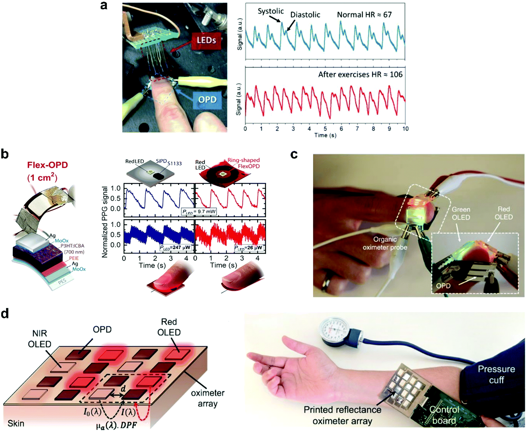 | ||
| Fig. 17 (a) Setup measuring the heart rate using OPDs and the recorded pulse signals.219 (b) Flexible OPD device geometry, schematics of S1133 Si-PD and ring-shaped flexible OPD PPG array (top) and comparison of reflection-mode PPG signals measured on a finger with both PDs driven by a red LED operated at different electrical power values.8 (c) Photograph of the OLED-OPD configuration for an all-organic pulse oximeter.2 (d) The schematic configuration and photograph of the reflectance oximeter array.3 (a) Reproduced with permission.219 Copyright 2019, WILEY-VCH GmbH. (b) Reproduced with permission.8 Copyright 2020. The American Association for the Advancement of Science. (c) Reproduced with permission.2 Copyright 2014, Springer Nature. (d) Reproduced with permission.3 Copyright 2018, the Authors. Published by PNAS. | ||
Pulse oximetry is another critical clinical application of PPG sensors for determining oxygen saturation in blood by optically quantifying the oxyhemoglobin (HbO2) and deoxyhemoglobin (Hb) concentrations.220 The first all-organic state-of-the-art pulse oximetry was reported by Lochner et al.2 This sensor used green and red organic LEDs (OLEDs) and two spatially separated OPDs (Fig. 17c). The OPDs were based on the PTB7:PC71BM blend and exhibited a low leakage current of ∼1 nA cm−2 at −2 V with a −3 dB frequency above 10 kHz. This device measured oxygenation accurately with relative errors as small as 2%. These metrics were sufficient for oximetry measurements and notable because it was created on a flexible substrate, with the active layers of the sensor deposited by spin-coating and printing. Khan et al. reported a large-area, 2D reflectance oximeter array based on a flexible organic optoelectronic system, which comprised four red, four NIR OLEDs, and eight OPDs (Fig. 17d).3 The OPD and OLED arrays were also fabricated by printing techniques. The implementation of the array provided 2D oxygenation mapping capability of an area rather than a single point, as demonstrated in previous related work.
In the aforementioned practical application, broadband OPDs and two spectrally distinct LEDs were employed to measure oxygen saturation. Attributing the OPD signal to one of the operated LEDs requires the modulation of the LED in the time domain and the correlated detection of the PD signals. Such a measurement setup needs elaborated measurement devices. Instead, employing two different narrowband OPDs would allow, on the one hand, to use a broadband light source and, on the other hand, to easily discriminate the spectral information since both wavelength ranges are measured separately. These advantages enable the use of a more straightforward measurement setup and increase the accuracy of the measurement analysis.
Image sensors
OPDs are increasingly investigated for imaging technologies, as their properties make them attractive candidates for applications such as VIS-color or NIR imaging, biometric imaging, fingerprint imaging, etc. OPDs offer cheaper processing methods, light, flexible, large (or small) areas and compatible device possibilities, and tunable optoelectronic properties – both at a material and device level. In 1998, Heeger et al. demonstrated the first full-color image sensors based on OPD arrays with P3OT:PC61BM polymer blend.221 After that, Rauch et al. extended the detection region up to 1.8 μm and realized an outstanding NIR image sensor based on PbS quantum dots (QDs) sensitized OPDs (Fig. 18a).170 For a 4 mm2 diode, accelerated aging test results showed minimum lifetimes of at least one year. Moreover, the NIR OPDs were integrated on top of commercially available a-Si active-matrix thin-film transistor (TFT) panels with 256 × 256 pixels and a photo of a butterfly was successfully reconstructed under an infrared illumination wavelength of 1310 nm. This work first demonstrated NIR imaging with hybrid photodetectors (HPD). Later, Büchele et al. designed another HPD for X-ray imaging by incorporating terbium-doped gadolinium oxysulfide scintillator (GOS:Tb) particles into a P3HT:PC61BM blend on an a-Si:H TFT array backplane with ITO contact pads (Fig. 18b).222 The X-ray-induced light emission from the scintillators is absorbed within hundreds of nanometers, which is negligible compared with the pixel size. Hence, the optical crosstalk is minimized. The X-ray image sensors exhibit an excellent spatial resolution of 4.75 linepairs per mm (lp mm−1) at a modulation transfer function of 0.2. Xu et al. reported 10,000-pixel OPDs focal plane arrays (FPAs) on the top of a 1.0 cm radius plastic hemisphere to imitate the structure of the human eye (Fig. 18c).223 The CuPc/C60 active layer was evaporated across the entire surface of the hemisphere, followed by deposition of a thin Ag strike layer and an array of Ag cathode columns on top. The impulse response of the OPDs is as fast as 20 ± 2 ns and measured a dynamic range of 20 dB, which makes the FPAs suitable for video-recording applications. Recently, Yokota et al. realized a flexible image sensor that integrated polycrystalline Si TFT readout circuits and NIR OPDs, capturing images of veins and fingerprints (Fig. 18d).224 Narrowband polymer PMDPP3T blended with PC61BM was used as the active layer, enabling a NIR OPD that exhibited a high sensitivity of 0.57 A W−1 when driven at −2 V at a NIR wavelength of 850 nm as is commonly done for vein authentication. This is equivalent to the sensitivity of Si photodiodes (0.5–0.7 A W−1). The conformable imager, with a resolution of 508 pixels per inch, a speed of 41 frames per second, and a total thickness of only 15 μm, can be further proven by the veins’ clear image in the finger fingerprint.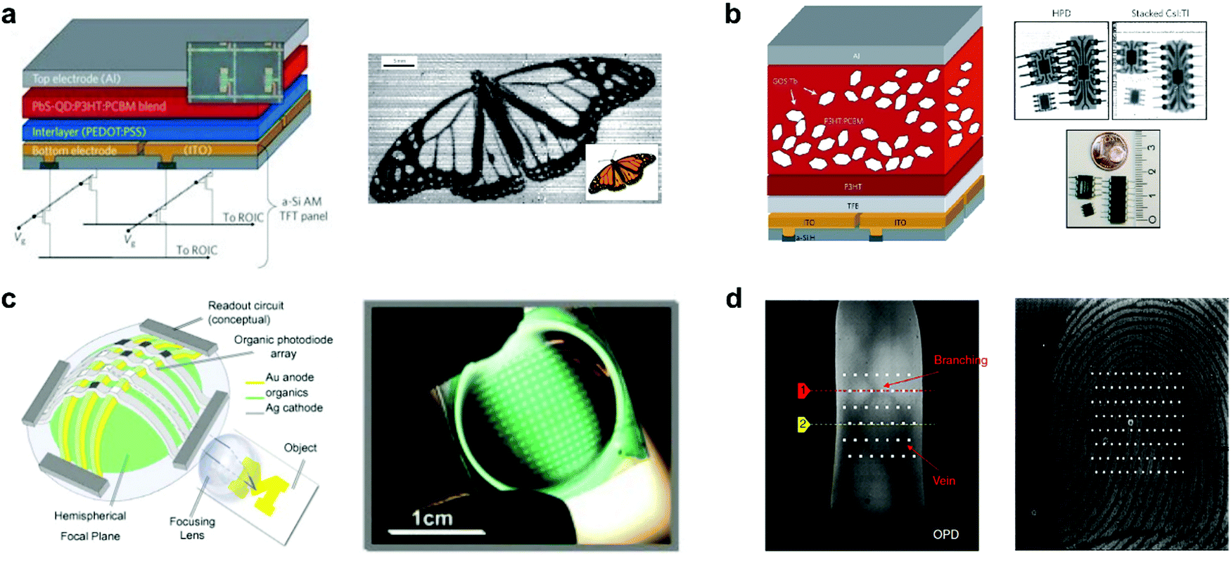 | ||
| Fig. 18 (a) Schematic of the NIR image sensor array based on OPDs doped with QDs and infrared shadow cast by a monarch butterfly.170 (b) Schematic of the X-ray image sensor with a high resolution based on organic BHJ doped with GOS:Tb.222 (c) Schematic and photograph of the hemispherical OPD-based FPA that imitates the human eye.223 (d) The image of veins and fingerprints through the flexible image sensor.224 (a) Reproduced with permission.170 Copyright 2009, Springer Nature. (b) Reproduced with permission.222 Copyright 2015, Springer Nature. (c) Reproduced with permission.223 Copyright 2008, Elsevier B.V. (d) Reproduced with permission.224 Copyright 2020, Springer Nature. | ||
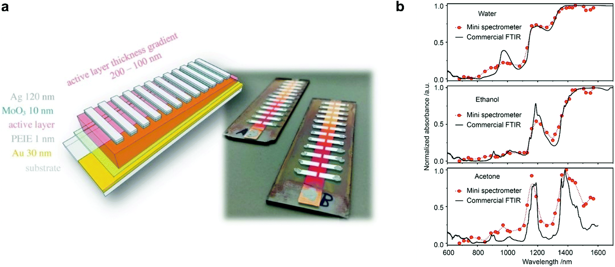 | ||
| Fig. 19 (a) A schematic and a photograph of a miniaturized spectrometer based on cavity enhanced NIR OPDs.74 (b) Absorption spectra of water, ethanol, and acetone measured using the miniaturized spectrometer compared to the spectra measured with a commercial Fourier transform infrared spectrometer.18 (a) Reproduced with permission.74 Copyright 2017, WILEY-VCH GmbH. (b) Reproduced with permission.18 Copyright 2021, American Chemical Society. | ||
Spectrometers
In 2017, Tang et al. employed a resonance optical cavity device architecture to fabricate a tunable wavelength-selection OPD exploiting weak sub-gap absorption of intermolecular CT states.74 This concept enables highly wavelength selective NIR OPDs with remarkable D* comparable with commercial inorganic counterparts. Based on this approach, a prototype miniaturized spectrometer was demonstrated by using a blade-coated active layer with gradient thickness (Fig. 19a). The transmittance spectrum of water was successfully measured, indicating a sufficient spectral resolution for a potential application in moisture detection. Recently, Yang et al. also utilized the cavity concept to build narrowband OPDs based on the PCDTPTSe:PC71BM active layer combined with a thick ZnO spacer.18 Similarly, a series of OPDs with varying response wavelengths in the range of 660–1600 nm was selected to prove the potential in spectroscopic applications. Using a halogen lamp as an external light source, the characteristic absorption features of water, ethanol, and acetone were well resolved, as shown in Fig. 19b.Miniaturized spectrometers are very attractive for mobile applications of spectroscopy to create new applications and products. In the NIR wavelength range, many characteristic absorption features of organic compounds are manifested and their analysis allows for qualitative and quantitative investigation of solids (reflection mode) and liquids (transmission or trans-reflection mode). Potential applications are the differentiation of materials such as fabrics (e.g., silk, wool, polyester, nylon), plastics (e.g., PET, PE, PVC, PP, PS), or many others. Such identification allows for a broad application in consumer and industry products, especially for the automatization of certain processes and machines. Another aspect is that NIR absorption and reflection features can be utilized to authenticate substances. This is becoming an important segment since many companies want to prevent the replication of their products by other manufacturers. For this purpose, native NIR reflection features of the product or specially designed, non-visible control-features can be utilized. An additional application in this regard can be the immediate identification of harmful and not-wanted substances such as drugs in liquids.
Finally, NIR spectroscopy is a very powerful method for quantitatively measuring the composition of solids and liquids, which is useful for countless applications. Here, NIR spectroscopy allows for a non-invasive, quick and precise analysis and thereby provides information that is usually rather difficult to obtain. For example, the ethanol content of a beverage can be precisely measured which is important not only for the producer but also for tax accounting and customs when trading beverages. For many processes, the composition of compounds is essential to sustain a very high production quality. One example is the qualification of fruit ripeness directly in the field to obtain the highest quality goods. Another example is the determination of moisture, which plays an important role in many automated processes, e.g., the production of corrugated cardboard. Applying spectroscopy allows for real-time, contactless measurement of water content in materials and is the prerequisite for further optimization of the production process. All in all, low-cost and highly integrated narrowband NIR-OPDs have a great potential to transform the well-established spectroscopy into the mobile application and bring the former laboratory know-how directly (or indirectly) to everyone. This transformation of an established technology has great potential for many innovative and smart products.
Conclusion and perspective
In this review, we summarized the status, recent progress and current challenges of narrowband OPDs. They have drawn much attention in the past decade thanks to advanced properties such as lightweight, flexibility, low-cost, large-area scalability, bio-compatibility and semi-transparency. These properties make narrowband OPDs potentially meet the demand of nowadays smarter and more efficient digital life. To date, the performance of state-of-the-art OPDs is dramatically improved, benefitting from the rapid progress in design and synthesis of new organic semiconductor compounds. In principle, narrowband OPDs rely on narrow-photo-absorbing materials covering the detection spectrum from the visible to the NIR range.20–22,72 However, such narrowband OPDs based on narrow-photo-absorbing materials with a specific bandgap are still suffering from a lack of material candidates, and also each material can only supply one specific spectral detection window. Fortunately, this issue was solved by the emerging strategies based on device architecture engineering, utilizing the usual organic broadband absorber. In 2015, charge collection narrowing OPDs were first introduced by using broadband-absorbing materials and a thick junction strategy, achieving red and NIR OPDs with FWHM of less than 100 nm.24 Afterwards, self-filtering narrowband OPDs composed of a depletion layer, a donor and a thin acceptor layer, forming a planar heterojunction, were demonstrated.26,83 In 2017, narrowband OPDs with the combination of a Fabry–Pérot microcavity and the charge-transfer state absorption of a bulk heterojunction were realized.27 Later on, based on such strategies, narrowband OPDs fabricated by either solution processing18,74 or vacuum thermal evaporation81,82,197,198 were explored extensively. The tunability of narrowband OPDs was radically improved, with the spectral detection window covering the visible (400–700 nm)81 and NIR (810–1665 nm) range.197 As application demonstrations, transmission spectra of different liquids (water, ethanol, acetone) were determined by spectrometers composed of narrowband OPDs.18,74 Having made this great progress, narrowband OPDs are already on the way to being commercialized for application-specific tasks (Fig. 20a), in particular for mobile usage of spectroscopy (Fig. 20b). Here, the key advantages of organic semiconductors such as simple and low-cost production, broad tunability of electrical and optical properties as well as competitive performance are the essential properties making this technology very promising. Nevertheless, there are still several important research perspectives for organic-semiconductor-based photodetectors: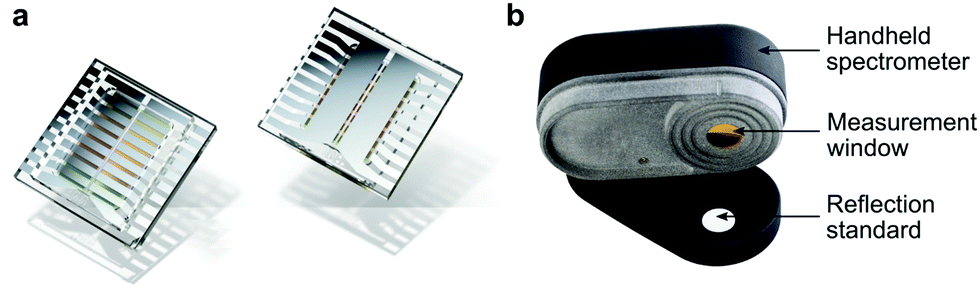 | ||
| Fig. 20 (a) Miniaturized spectrometer OPD-chip in top (left side) and bottom view (right side), being commercialized by the Senorics GmbH (Dresden, Germany, https://senorics.com/). The spectrometer chip is composed of 16 independent narrowband NIR-OPDs with an overall area of 121 mm2 (11 mm × 11 mm). The OPD-chip is bottom illuminated and its upper side is encapsulated by a glass lid to prevent ambient influences. (b) A handheld spectrometer employing the NIR OPD-chip from figure (a) and a NIR light source, realized by the same company. During measurement, NIR light shines through the measurement window onto the target object, which is exposed in front of the window and the reflected light is analyzed by the chip. The lid of the handheld spectrometer has an integrated reflection standard which is used to perform a white reference measurement. Reproduced with permission. Copyright, Senorics GmbH. | ||
• Obviously, there will be always a need for better materials, with properties like high absorption coefficient, broad- or narrowband absorption depending on device principle, and excellent charge carrier generation. In particular, there is a need for stronger absorbers in the NIR up to 2000 nm since many applications require signal detection in this spectral range. Besides the optical properties mentioned above, these materials also need to have good processability, low synthesis cost and good photostability.
• There is a need for novel device principles, which allow to realize specific properties, such as high detectivity, narrowband operation, and high speeds or a combination thereof. For instance, there are many principles which have not yet been intensively investigated, such as two- or three-dimensional patterning of structures.
• For devices working in photovoltaic mode, understanding and controlling reverse current is still a key issue. The rather complicated nanostructured bulk heterojunctions employed in most of these devices make it difficult to understand traps in particular at the interfaces. It is essential to understand the intrinsic limits in terms of reverse current and avoid extrinsic currents.
• The field of OPDs with gain is still not well understood. Many of the devices show quite good device parameters, without microscopic understanding of the device principle. Only such an understanding will allow for a directed optimization.
• To fully harvest the intrinsic advantages of organic electronics, the integration of OPDs with organic transistors is of great interest. This could provide immediate amplification of the detector signal, or even a certain in situ pre-processing leading towards more autonomous organic sensor modules.
• It would be highly desirable to develop organic detectors with speeds in the GHz range and beyond. Recently, first GHz organic pin-diodes have been shown160 and it remains a challenge to prove such operation speeds for optical detection.
• Finally, the temporal stability of OPDs has been much less investigated than their organic counterparts (i.e. organic light emitting diodes and organic solar cells). There is hope that OPDs are very stable since their relatives, the organic solar cells, achieve encouraging operational stabilities.85,225
We are convinced that these exciting perspectives will stimulate further research on OPDs. As the success of organic light emitting diode displays has shown that the materials and deposition methods are ready for mass-scale manufacturing. In a sensor-hungry world, OPDs will thus have a bright future!
Conflicts of interest
Karl Leo is shareholder of Senorics GmbH, a company active in organic photodetectors.Appendix – performance metrics of organic photodetectors
A fair comparison of different PD technologies and a valid evaluation of photodetecting devices requires a careful determination of fundamental performance metrics. Here, we summarize the performance metrics of PDs. In the formulas below the corresponding units are indicated in parenthesis.Quantum efficiency
The quantum efficiency of a photodiode indicates the amount of photogenerated charge carriers produced by the PD when illuminating it with photons of a specific wavelength. By integrating the quantum efficiency over the electromagnetic spectrum of the light source, the total current produced by the PD can be evaluated. There are two types of quantum efficiencies utilized to characterize PDs:• The external quantum efficiency (EQE) is given by the ratio of the number of charge carriers extracted at the electrodes of a PD to the total number of incident photons impinging onto the device:
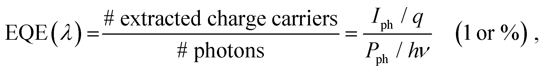 | (6) |
• In contrast to the EQE, the internal quantum efficiency (IQE) refers only to photons that are absorbed by the active layer. Thus, it refers to the ratio of the total number of charge carriers extracted from the device to the number of incident photons that are absorbed in the photo-active layer. The IQE of a PD yields the overall efficiency of the charge carrier generation, dissociation, recombination and extraction processes versus the wavelength or energy of incident photons.87 Often, IQE is calculated from the EQE by measuring the transmission  and reflection
  of a PD as expressed in eqn (7). This approach neglects parasitic absorption and the interference of an optical cavity, which is introduced by the mirror-like electrodes. Armin et al. carefully treated this issue and gave a more precise solution to calculate the IQE as formulated in eqn (8).87 The metallic electrode is assumed to be opaque, hence,
  is not accounted for in eqn (8). The parasitic absorption (Aparasitic) and the optical field distribution of photodiodes can be determined by transfer matrix simulations.87
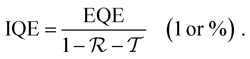 | (7) |
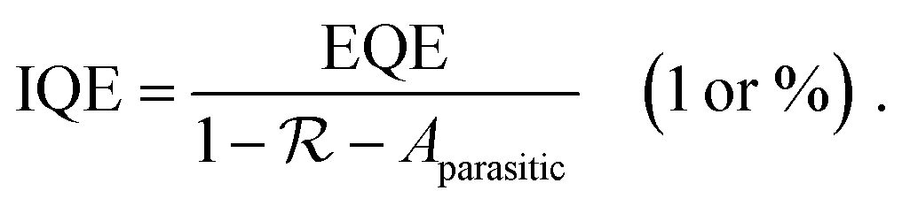 | (8) |
Responsivity
The responsivity (R), also referred to as spectral response, is defined as the ratio of the generated photocurrent (Iph) to the incident light power (Pph) at a corresponding wavelength. In practice, R is often calculated from EQE.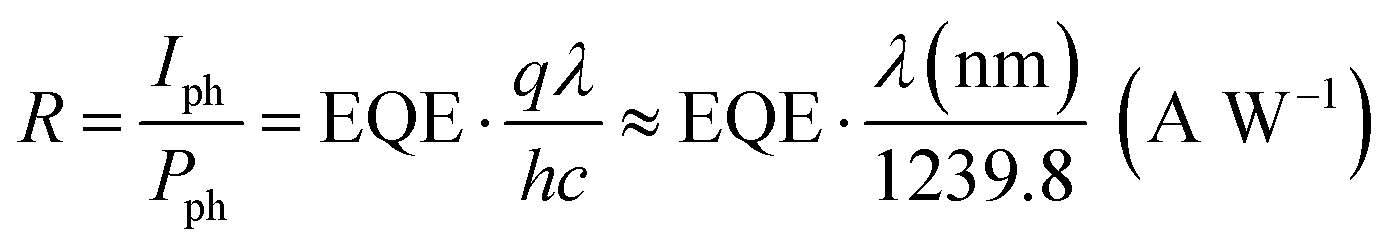 | (9) |
Noise current (Inoise) and noise equivalent power (NEP)
In a real measurements, the final criterion to detect a weak signal is the ratio of signal to noise. It is therefore very important to understand the sources of noise in PDs. Inclusion of noise leads from the responsivity to the detectivity which is discussed below.There are several sources contributing to the device noise and the current associated to it, Inoise. The white noise components (frequency independent) entail the thermal noise (Ithermal), also called Johnson-Nyquist noise, the shot noise (Ishot) and the generation-recombination noise (IG–R). Additionally, pink noise components (frequency dependent) are also observed. The most known but least understood pink noise is the flicker or simply “one over f” noise (I1/f noise), which is commonly observed in the low frequency regime of the spectral noise density. Together, these noise components determine the detection limit for low intensity light.138,226
• Ithermal exists in any resistive component and is generated by the random thermal motion of charge carriers. In OPDs, it can be correlated with the total parallel resistance (Rp) including shunt resistance (Rshunt) and effective diode resistance at zero bias in the circuit. In most conditions, Rshunt dominates the Rp.138 Therefore, Ithermal can be formulated into:
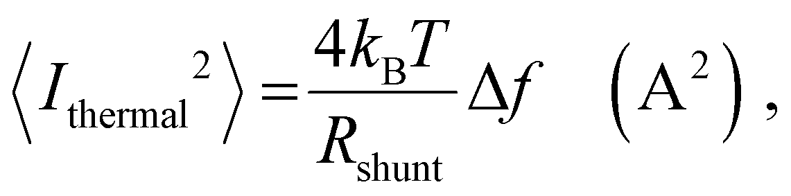 | (10) |
• Ishot arises from the discrete character of charge carriers when overcoming energy barriers. In p–n, p–i–n, or Schottky junctions, for example, the current suffers small time-dependent variations caused by charge carriers individually crossing depletion regions or the Schottky injection barrier. Ishot is therefore proportional to the average dark current Id (without illumination):136
| 〈Ishot2〉 = 2qIdΔf (A2). | (11) |
• IG–R is the result of temporal variation of the background photon flux, which leads to a variation in the charge carrier concentration, thereby affecting the photoconductivity in photoconductors or the photocurrent in photodiodes. Although the G–R noise is white in nature, a pink behavior can be observed depending on the dynamics of the system. For band-to-band processes, for example, G–R noise becomes frequency dependent at the frequency corresponding to the reciprocal of the transit time.228 Because G–R noise in photodiodes can be expressed with a mathematically equivalent expression to that of shot noise,229 both noise sources are often thought to be the same, with the former attributed to photoconductors and the latter to photodiodes. The confusion arises from the fact that in photodiodes operated under reverse bias, only generation is relevant, since charges are swept out of the device and do not recombine.228 In photoconductors, however, both processes take place randomly. Yet, strictly speaking, the physical nature of these two sources of noise is different. Finally, IG–R is expressed by eqn (12), assuming the mathematical form of eqn (11) for photodiodes operating under reverse bias.228,229
| 〈IG–R2〉 = 4qIdΔf (A2). | (12) |
• 1/f noise: the spectral distribution of flicker noise can be empirically described by eqn (13), where K is a normalization constant, a ≈ 2 and, b ≈ 1.227,230 While physical explanations have been given for the aforementioned sources of noise, 1/f noise remains mysterious, being reflected in the lack of a proper name. It is common to observe a frequency dependent increase of the noise at low frequencies, which follows a 1/f behavior. The most accepted explanation for the origin of this effect is related to surface traps and bulk traps, leading to a fluctuation in the charge carrier density, as charges fall into and are released from these states. However, none of these effects have been completely clarified.227 In organic semiconductor devices, 1/f noise is introduced by resistance fluctuation and intrinsically caused by either charge carrier fluctuation or mobility fluctuation.226,231
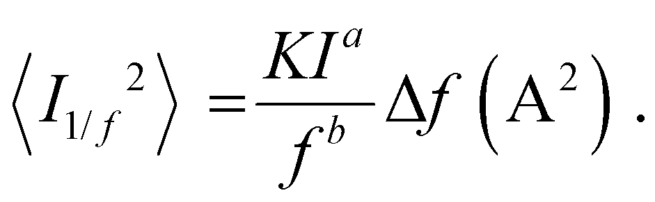 | (13) |
 | (14) |
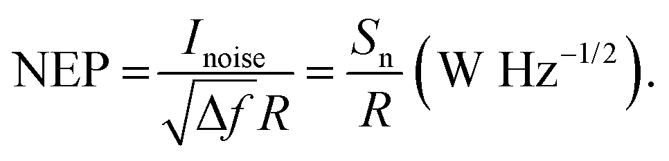 | (15) |
Specific detectivity (D*)
Due to the counterintuitive character of the NEP, where a better PD has lower NEP, its inverse was introduced, named detectivity (D). Additionally, it is possible to show that D is inversely proportional , where A is device area in cm2.37,232 Therefore, in order to compare different PDs, D is normalized by
  , being referred to as specific detectivity (D*).
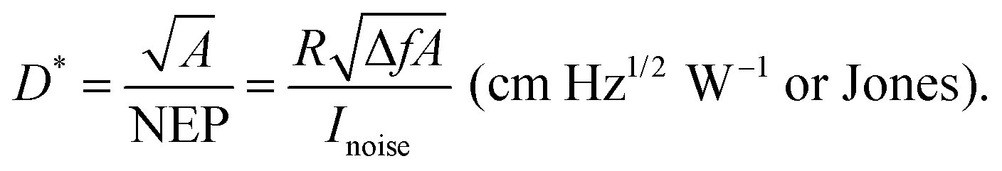 | (16) |
Dynamic range (DR) and linear dynamic range (LDR)
Every PD operates in an optical input range where its photoresponse can be accurately measured and predicted. This range, from the lowest to the highest optical input which generates such a predictable photoresponse, is referred to as dynamic range (DR). Often, DR is taken from the region where the photoresponse is proportional to a power law of the optical input, i.e. I ∝ Irrβ, where I and Irr are the photocurrent and irradiance, respectively. Such dependence corresponds to a linear behavior in the double-log plot. Photoconductors with photogain (G) higher than unity show a sublinear DR with β < 1,34,234 while photodiodes often show a rather linear photoresponse referred to as linearity or linear dynamic range (LDR) with β = 1. Physically, LDR means that within this range, the processes of charge carrier generation and recombination are independent of the light intensity, which is translated to a linear dependence of the photoresponse on the latter. While a linearity is desired for applications due to the facilitated device calibration, a non-linear photoresponse can likewise be used, as long as the non-linearity is reproducible and, therefore, predictable. DR and LDR can be expressed respectively as: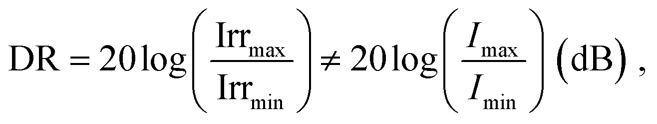 | (17) |
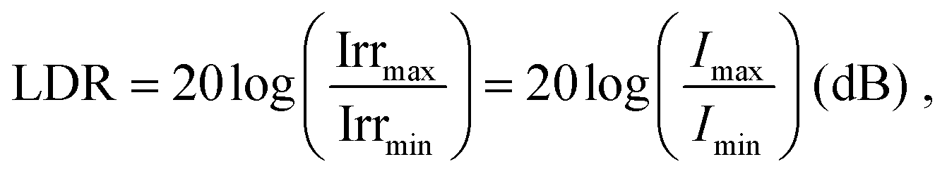 | (18) |
Response speed
The response speed represents how fast PDs respond to the incident optical signal, which determines potential applications of PDs like imaging,1,238 hemodynamics monitoring,219 and high speed optical communications.73,160 Response speed can be characterized by transient photocurrent measurements, where, by applying a short pulse of an optical signal, the rising (τr) and falling (τf) time of the PDs are revealed. τr is defined as the rising time of photocurrent from 10% to 90% of the maximum value when turning on the illumination. Vice versa, τf is defined as the time for the photocurrent to fall from 90% to 10% of the maximum value when turning off the illumination. The response speed is correlated to the charge carrier separation, dissociation, recombination, and extraction. For example, the conductivity of the electrodes influences the transit time of charge carriers;239,240 an electron or hole blocking layer affects charge carrier extraction or injection.63,241−3 dB bandwidth (f−3dB)
Another important parameter for evaluating the response speed of PDs is the frequency response being quantified by the −3 dB bandwidth (f−3dB). It is defined as the modulation frequency of the optical signal at which the measured photocurrent decreases to −3 dB (1/√2 = 70.7%) of its low frequency value. The f−3dB is correlated to the carrier transit time (τtr) and the RC-time of the equivalent circuit as: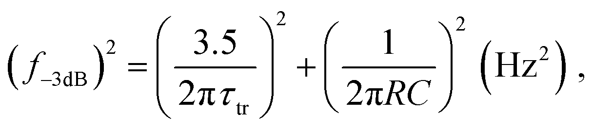 | (19) |
Spectral selectivity and spectral rejection ratio (SRR)
Additionally to the discussed figures-of-merit, there are two more parameters that need to be introduced for evaluating narrowband PDs. As depicted in Fig. 2, one is the full width at half maximum (FWHM), denoting the selectivity of PDs. The narrower the FWHM, the higher the selectivity. FWHM can either be defined from the EQE curve (FWHMEQE) or the responsivity curve (FWHMR). The other important parameter is the spectral rejection ratio (SRR), describing the ratio of the peak responsivity (Rpeak) in the target spectral window to the responsivity outside this measurement window (Rout), expressed as:73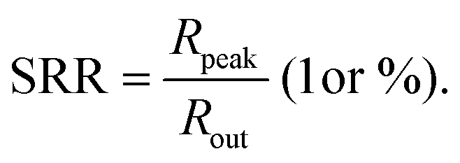 | (20) |
Abbreviations
| PD | Photodetector |
| OPD | Organic PD |
| PC-OPD | Photoconductor OPD |
| PM-OPD | Photomultiplication OPD |
| PT-OPD | Phototransistor OPD |
| CT-OPD | Cavity-enhanced charge-transfer (CT) state based OPD |
| PV-OPD | Photovoltaic OPD |
| OSC | Organic solar cell |
| VIS | Visible |
| NIR | Near infrared |
| R | Spectral photoresponse |
| EQE | External quantum efficiency |
| D* | Specific detectivity |
| FWHM | Full width at half maximum |
| SRR | Spectral rejection ratio |
| J D | Reverse dark current |
| J 0 | Saturation current |
Acknowledgements
We acknowledge Jakob Wolansky and Louis Conrad Winkler for fruitful discussions and feedback to our manuscript. We further acknowledge the Senorics GmbH for their permission to include pictures of their miniaturized OPD-chip and spectrometer technology. Additionally, we thank the BMBF for funding through the projects “Pergamon” (16ME0012) and “Flexmonirs” (01DR20008A) and the German Research Foundation (DFG) through project “Coherent Perfect Light for Organic Microdevices” (442597684). Y. Wang acknowledges the Graduate Academy of Technische Universität Dresden for funding and S. Xing acknowledges the financial support via the China Scholarship Council (no. 201706070125).References
- Y. L. Wu, K. Fukuda, T. Yokota and T. Someya, Adv. Mater., 2019, 31, 1903687 CrossRef CAS.
- C. M. Lochner, Y. Khan, A. Pierre and A. C. Arias, Nat. Commun., 2014, 5, 5745 CrossRef CAS.
- Y. Khan, D. Han, A. Pierre, J. Ting, X. Wang, C. M. Lochner, G. Bovo, N. Yaacobi-Gross, C. Newsome, R. Wilson and A. C. Arias, Proc. Natl. Acad. Sci. U. S. A., 2018, 115, E11015–E11024 CrossRef CAS.
- Y. Wang, J. Benduhn, L. Baisinger, C. Lungenschmied, K. Leo and D. Spoltore, ACS Appl. Mater. Interfaces, 2021, 13, 23239–23246 CrossRef CAS.
- M. Babics, H. Bristow, W. Zhang, A. Wadsworth, M. Neophytou, N. Gasparini and I. McCulloch, J. Mater. Chem. C, 2021, 9, 2375–2380 RSC.
- P. C. Y. Chow and T. Someya, Adv. Mater., 2020, 32, 1902045 CrossRef CAS.
- J. J. Kim, Y. Wang, H. Wang, S. Lee, T. Yokota and T. Someya, Adv. Funct. Mater., 2021, 2009602 CrossRef CAS.
- C. Fuentes-Hernandez, W. F. Chou, T. M. Khan, L. Diniz, J. Lukens, F. A. Larrain, V. A. Rodriguez-Toro and B. Kippelen, Science, 2020, 370, 698–701 CrossRef CAS.
- X. Xu, X. Zhou, K. Zhou, Y. Xia, W. Ma and O. Inganäs, Adv. Funct. Mater., 2018, 28, 1805570 CrossRef.
- M. Heuken and N. Meyer, Org. Electron. Mater. Manuf. Appl., 2006, 10, 203–232 Search PubMed.
- F. C. Krebs, Sol. Energy Mater. Sol. Cells, 2009, 93, 465–475 CrossRef CAS.
- C. Girotto, D. Moia, B. P. Rand and P. Heremans, Adv. Funct. Mater., 2011, 21, 64–72 CrossRef CAS.
- D. Li and L. J. Guo, Appl. Phys. Lett., 2006, 88, 063513 CrossRef.
- Y. Xia, L. E. Aguirre, X. Xu and O. Inganäs, Adv. Electron. Mater., 2020, 6, 1901017 CrossRef CAS.
- A. J. P. Theuwissen, Solid State Electron., 2008, 52, 1401–1406 CrossRef CAS.
- X. Gong, M. Tong, Y. Xia, W. Cai, J. S. Moon, Y. Cao, G. Yu, C. L. Shieh, B. Nilsson and A. J. Heeger, Science, 2009, 325, 1665–1667 CrossRef CAS.
- F. Verstraeten, S. Gielen, P. Verstappen, J. Raymakers, H. Penxten, L. Lutsen, K. Vandewal and W. Maes, J. Mater. Chem. C, 2020, 8, 10098–10103 RSC.
- J. Yang, J. Huang, R. Li, H. Li, B. Sun, Q. Lin, M. Wang, Z. Ma, K. Vandewal and Z. Tang, Chem. Mater., 2021, 33, 5147–5155 CrossRef CAS.
- W. Li, H. Guo, Z. Wang and G. Dong, J. Phys. Chem. C, 2017, 121, 15333–15338 CrossRef CAS.
- W. Li, D. Li, G. Dong, L. Duan, J. Sun, D. Zhang and L. Wang, Laser Photonics Rev., 2016, 10, 473–480 CrossRef CAS.
- D. M. Lyons, A. Armin, M. Stolterfoht, R. C. R. Nagiri, R. D. Jansen-Van Vuuren, B. N. Pal, P. L. Burn, S. C. Lo and P. Meredith, Org. Electron., 2014, 15, 2903–2911 CrossRef CAS.
- H. Zhang, S. Jenatsch, J. De Jonghe, F. Nuësch, R. Steim, A. C. Véron and R. Hany, Sci. Rep., 2015, 5, 9439 CrossRef CAS.
- T. P. Osedach, A. Iacchetti, R. R. Lunt, T. L. Andrew, P. R. Brown, G. M. Akselrod and V. Bulović, Appl. Phys. Lett., 2012, 101, 113303 CrossRef.
- A. Armin, R. D. J. Vuuren, N. Kopidakis, P. L. Burn and P. Meredith, Nat. Commun., 2015, 6, 6343 CrossRef CAS.
- W. Wang, F. Zhang, M. Du, L. Li, M. Zhang, K. Wang, Y. Wang, B. Hu, Y. Fang and J. Huang, Nano Lett., 2017, 17, 1995–2002 CrossRef CAS.
- B. Xie, R. Xie, K. Zhang, Q. Yin, Z. Hu, G. Yu, F. Huang and Y. Cao, Nat. Commun., 2020, 11, 2871 CrossRef CAS.
- B. Siegmund, A. Mischok, J. Benduhn, O. Zeika, S. Ullbrich, F. Nehm, M. Böhm, D. Spoltore, H. Fröb, C. Körner, K. Leo and K. Vandewal, Nat. Commun., 2017, 8, 15421 CrossRef CAS.
- Y. Lin, M. I. Nugraha, Y. Firdaus, A. D. Scaccabarozzi, F. Aniés, A. H. Emwas, E. Yengel, X. Zheng, J. Liu, W. Wahyudi, E. Yarali, H. Faber, O. M. Bakr, L. Tsetseris, M. Heeney and T. D. Anthopoulos, ACS Energy Lett., 2020, 5, 3663–3671 CrossRef CAS.
- Y. Lin, Y. Firdaus, F. H. Isikgor, M. I. Nugraha, E. Yengel, G. T. Harrison, R. Hallani, A. El-Labban, H. Faber, C. Ma, X. Zheng, A. Subbiah, C. T. Howells, O. M. Bakr, I. McCulloch, S. De Wolf, L. Tsetseris and T. D. Anthopoulos, ACS Energy Lett., 2020, 5, 2935–2944 CrossRef CAS.
- Y. Cui, H. Yao, J. Zhang, K. Xian, T. Zhang, L. Hong, Y. Wang, Y. Xu, K. Ma, C. An, C. He, Z. Wei, F. Gao and J. Hou, Adv. Mater., 2020, 32, 1908205 CrossRef CAS.
- Y. Cai, Y. Li, R. Wang, H. Wu, Z. Chen, J. Zhang, Z. Ma, X. Hao, Y. Zhao, C. Zhang, F. Huang and Y. Sun, Adv. Mater., 2021, 33, 2101733 CrossRef CAS.
- J. Lee, S. J. Ko, H. Lee, J. Huang, Z. Zhu, M. Seifrid, J. Vollbrecht, V. V. Brus, A. Karki, H. Wang, K. Cho, T. Q. Nguyen and G. C. Bazan, ACS Energy Lett., 2019, 4, 1401–1409 CrossRef CAS.
- W. Peng, Y. Liu, C. Wang, R. Hu, J. Zhang, D. Xu and Y. Wang, J. Mater. Chem. C, 2015, 3, 5073 RSC.
- R. Reuter and H. Franke, Appl. Phys. B: Photophys. Laser Chem., 1989, 48, 219–224 CrossRef.
- J. H. Vella, L. Huang, N. Eedugurala, K. S. Mayer, T. N. Ng and J. D. Azoulay, Sci. Adv., 2021, 7, eabg2418 CrossRef CAS.
- M. Daanoune, R. Clerc, B. Flament and L. Hirsch, J. Appl. Phys., 2020, 127, 055502 CrossRef CAS.
- S. M. Sze and L. K. Ng, Physics of Semiconductor Devices, John Wiley & Sons, 3rd edn, 2006 Search PubMed.
- G. Konstantatos, I. Howard, A. Fischer, S. Hoogland, J. Clifford, E. Klem, L. Levina and E. H. Sargent, Nature, 2006, 442, 180–183 CrossRef CAS.
- S. R. Forrest, Nature, 2004, 428, 911–918 CrossRef CAS.
- K. Walzer, B. Männig, M. Pfeiffer and K. Leo, Chem. Rev., 2007, 107, 1233–1271 CrossRef CAS.
- A. Tsumura, H. Koezuka and T. Ando, Appl. Phys. Lett., 1986, 49, 1210–1212 CrossRef CAS.
- B. Lucas, T. Trigaud and C. Videlot-Ackermann, Polym. Int., 2012, 61, 374–389 CrossRef CAS.
- B. Yang, Y. Wang, L. Li, J. Zhang, J. Wang, H. Jiao, D. Hao, P. Guo, S. Zeng, Z. Hua and J. Huang, Adv. Funct. Mater., 2021, 2103787 CrossRef CAS.
- D. Q. Tan, Adv. Funct. Mater., 2020, 30, 1808567 CrossRef CAS.
- H. Ren, J. De Chen, Y. Q. Li and J. X. Tang, Adv. Sci., 2021, 8, 2002418 CrossRef CAS.
- J. Reynaert, V. I. Arkhipov, P. Heremans and J. Poortmans, Adv. Funct. Mater., 2006, 16, 784–790 CrossRef CAS.
- M. Hiramoto, T. Imahigashi and M. Yokoyama, Appl. Phys. Lett., 1994, 64, 187–189 CrossRef CAS.
- W. T. Hammond, J. P. Mudrick and J. Xue, J. Appl. Phys., 2014, 116, 214501 CrossRef.
- R. Nie, X. Deng, L. Feng, G. Hu, Y. Wang, G. Yu and J. Xu, Small, 2017, 13, 1603260 CrossRef.
- J. Huang, J. Lee, M. Schrock, A. L. Dixon, A. T. Lill, K. Cho, G. C. Bazan and T. Q. Nguyen, Mater. Horiz., 2020, 7, 3234 RSC.
- T. Katsume, M. Hiramoto and M. Yokoyama, Appl. Phys. Lett., 1996, 69, 3722–3724 CrossRef CAS.
- H. Rost and H. H. Hörhold, Phys. Rev. B: Condens. Matter Mater. Phys., 1999, 59, 1964–1972 CrossRef.
- G. Matsunobu, Y. Oishi, M. Yokoyama and M. Hiramoto, Appl. Phys. Lett., 2002, 81, 1321–1322 CrossRef CAS.
- F. C. Chen, S. C. Chien and G. L. Cious, Appl. Phys. Lett., 2010, 97, 103301 CrossRef.
- R. Dong, C. Bi, Q. Dong, F. Guo, Y. Yuan, Y. Fang, Z. Xiao and J. Huang, Adv. Opt. Mater., 2014, 2, 549–554 CrossRef CAS.
- L. Shen, Y. Fang, Q. Dong, Z. Xiao and J. Huang, Appl. Phys. Lett., 2015, 106, 023301 CrossRef.
- X. Li, X. Li, S. Wang and Y. Xiao, J. Mater. Chem. C, 2016, 4, 5584 RSC.
- L. Li, F. Zhang, J. Wang, Q. An, Q. Sun, W. Wang, J. Zhang and F. Teng, Sci. Rep., 2015, 5, 9181 CrossRef CAS.
- L. Li, F. Zhang, W. Wang, Y. Fang and J. Huang, Phys. Chem. Chem. Phys., 2015, 17, 30712 RSC.
- J. Huang and Y. Yang, Appl. Phys. Lett., 2007, 91, 203505 CrossRef.
- Y. Fang, F. Guo, Z. Xiao and J. Huang, Adv. Opt. Mater., 2014, 2, 348–353 CrossRef CAS.
- J. W. Lee, D. Y. Kim and F. So, Adv. Funct. Mater., 2015, 25, 1233–1238 CrossRef CAS.
- W. T. Hammond and J. Xue, Appl. Phys. Lett., 2010, 97, 073302 CrossRef.
- D. Yang, X. Zhou, Y. Wang, A. Vadim, S. M. Alshehri, T. Ahamad and D. Ma, J. Mater. Chem. C, 2016, 4, 2160 RSC.
- Z. Zhao, C. Xu, L. Niu, X. Zhang and F. Zhang, Laser Photonics Rev., 2020, 14, 2000262 CrossRef CAS.
- P. Peumans, A. Yakimov and S. R. Forrest, J. Appl. Phys., 2003, 93, 3693–3723 CrossRef CAS.
- O. V. Mikhnenko, P. W. M. Blom and T. Q. Nguyen, Energy Environ. Sci., 2015, 8, 1867 RSC.
- C. W. Tang, Appl. Phys. Lett., 1986, 48, 183–185 CrossRef CAS.
- G. Yu, J. Gao, J. C. Hummelen, F. Wudl and A. J. Heeger, Science, 1995, 270, 1789–1791 CrossRef CAS.
- J. J. M. Halls, C. A. Walsh, N. C. Greenham, E. A. Marseglia, R. H. Friend, S. C. Morattlt and A. B. Holmes, Nature, 1995, 376, 498–500 CrossRef CAS.
- X. Ren, F. Yang, X. Gao, S. Cheng, X. Zhang, H. Dong and W. Hu, Adv. Energy Mater., 2018, 8, 1801223 Search PubMed.
- M. G. Han, K. B. Park, X. Bulliard, G. H. Lee, S. Yun, D. S. Leem, C. J. Heo, T. Yagi, R. Sakurai, T. Ro, S. J. Lim, S. Sul, K. Na, J. Ahn, Y. W. Jin and S. Lee, ACS Appl. Mater. Interfaces, 2016, 8, 26143–26151 CrossRef CAS.
- Z. Lan, Y. S. Lau, Y. Wang, Z. Xiao, L. Ding, D. Luo and F. Zhu, Adv. Opt. Mater., 2020, 2001388 CrossRef CAS.
- Z. Tang, Z. Ma, A. Sánchez-Díaz, S. Ullbrich, Y. Liu, B. Siegmund, A. Mischok, K. Leo, M. Campoy-Quiles, W. Li and K. Vandewal, Adv. Mater., 2017, 29, 1702184 CrossRef.
- S. Xing, V. C. Nikolis, J. Kublitski, E. Guo, X. Jia, Y. Wang, D. Spoltore, K. Vandewal, H. Kleemann, J. Benduhn and K. Leo, Adv. Mater., 2021, 2102967 CrossRef CAS.
- R. Lukac, J. Real-Time Image Process., 2006, 1, 45–52 CrossRef.
- S. Nishiwaki, T. Nakamura, M. Hiramoto, T. Fujii and M. A. Suzuki, Nat. Photonics, 2013, 7, 240–246 CrossRef.
- M. Dandin, P. Abshire and E. Smela, Lab Chip, 2007, 7, 955–977 RSC.
- Q. Lin, A. Armin, P. L. Burn and P. Meredith, Nat. Photonics, 2015, 9, 687–694 CrossRef CAS.
- M. S. Ünlü and S. Strite, J. Appl. Phys., 1995, 78, 607–639 CrossRef.
- J. Wang, S. Ullbrich, J. L. Hou, D. Spoltore, Q. Wang, Z. Ma, Z. Tang and K. Vandewal, ACS Photonics, 2019, 6, 1393–1399 CrossRef CAS.
- Y. Wang, B. Siegmund, Z. Tang, Z. Ma, J. Kublitski, S. Xing, V. C. Nikolis, S. Ullbrich, Y. Li, J. Benduhn, D. Spoltore, K. Vandewal and K. Leo, Adv. Opt. Mater., 2021, 9, 2001784 CrossRef CAS.
- S. Xing, X. Wang, E. Guo, H. Kleemann and K. Leo, ACS Appl. Mater. Interfaces, 2020, 12, 13061–13067 CrossRef CAS.
- J. L. Bredas, AIP Conf. Proc., 2013, 1519, 55–58 CrossRef CAS.
- A. Armin, W. Li, O. J. Sandberg, Z. Xiao, L. Ding, J. Nelson, D. Neher, K. Vandewal, S. Shoaee, T. Wang, H. Ade, T. Heumüller, C. Brabec and P. Meredith, Adv. Energy Mater., 2021, 11, 20003570 CrossRef.
- M. L. Tietze, J. Benduhn, P. Pahner, B. Nell, M. Schwarze, H. Kleemann, M. Krammer, K. Zojer, K. Vandewal and K. Leo, Nat. Commun., 2018, 9, 1182 CrossRef.
- A. Armin, M. Velusamy, P. Wolfer, Y. Zhang, P. L. Burn and P. Meredith, ACS Photonics, 2014, 1, 173–181 CrossRef CAS.
- Q. D. Ou, Y. Q. Li and J. X. Tang, Adv. Sci., 2016, 3, 1–25 Search PubMed.
- Y. Park, K. Vandewal and K. Leo, Small Methods, 2018, 2, 1800123 CrossRef.
- D. E. Markov, J. C. Hummelen, P. W. M. Blom and A. B. Sieval, Phys. Rev. B: Condens. Matter Mater. Phys., 2005, 72, 045216 CrossRef.
- J. J. M. Halls, K. Pichler and R. H. Friend, J. Appl. Phys., 1996, 68, 3120–3122 CAS.
- W. A. Luhman and R. J. Holmes, Adv. Funct. Mater., 2011, 21, 764–771 CrossRef CAS.
- S. M. Menke and R. J. Holmes, Energy Environ. Sci., 2014, 7, 499–512 RSC.
- Y. Terao, H. Sasabe and C. Adachi, Appl. Phys. Lett., 2007, 90, 1–3 CrossRef.
- G. Wei, R. R. Lunt, K. Sun, S. Wang, M. E. Thompson and S. R. Forrest, Nano Lett., 2010, 10, 3555–3559 CrossRef CAS.
- T. Förster, Discuss. Faraday Soc., 1959, 27, 7–17 RSC.
- D. L. Dexter, J. Chem. Phys., 1953, 21, 836–850 CrossRef CAS.
- G. D. Scholes, Annu. Rev. Phys. Chem., 2003, 54, 57–87 CrossRef CAS.
- R. Koeppe and N. S. Sariciftci, Photochem. Photobiol. Sci., 2006, 5, 1122–1131 CrossRef CAS.
- S. Raisys, K. Kazlauskas, M. Daskeviciene, T. Malinauskas, V. Getautis and S. Jursenas, J. Mater. Chem. C, 2014, 2, 4792–4798 RSC.
- R. R. Lunt, J. B. Benziger and S. R. Forrest, Adv. Mater., 2010, 22, 1233–1236 CrossRef CAS.
- S. M. Menke, W. A. Luhman and R. J. Holmes, Nat. Mater., 2013, 12, 152–157 CrossRef CAS.
- S. Athanasopoulos, E. Hennebicq, D. Beljonne and A. B. Walker, J. Phys. Chem. C, 2008, 112, 11532–11538 CrossRef CAS.
- Y. Zhong, M. Causa’, G. J. Moore, P. Krauspe, B. Xiao, F. Günther, J. Kublitski, R. Shivhare, J. Benduhn, E. BarOr, S. Mukherjee, K. M. Yallum, J. Réhault, S. C. B. Mannsfeld, D. Neher, L. J. Richter, D. M. DeLongchamp, F. Ortmann, K. Vandewal, E. Zhou and N. Banerji, Nat. Commun., 2020, 11, 833 CrossRef CAS.
- R. A. Marcus, J. Phys. Chem., 1989, 93, 3078–3086 CrossRef CAS.
- A. J. Ward, A. Ruseckas, M. M. Kareem, B. Ebenhoch, L. A. Serrano, M. Al-Eid, B. Fitzpatrick, V. M. Rotello, G. Cooke and I. D. W. Samuel, Adv. Mater., 2015, 27, 2496–2500 CrossRef CAS.
- T. M. Clarke and J. R. Durrant, Chem. Rev., 2010, 110, 6736–6767 CrossRef CAS.
- T. M. Clarke, A. M. Ballantyne, J. Nelson, D. D. C. Bradley and J. R. Durrant, Adv. Funct. Mater., 2008, 18, 4029–4035 CrossRef CAS.
- V. C. Nikolis, J. Benduhn, F. Holzmueller, F. Piersimoni, M. Lau, O. Zeika, D. Neher, C. Koerner, D. Spoltore and K. Vandewal, Adv. Energy Mater., 2017, 7, 1700855 CrossRef.
- S. Liu, J. Yuan, W. Deng, M. Luo, Y. Xie, Q. Liang, Y. Zou, Z. He, H. Wu and Y. Cao, Nat. Photonics, 2020, 14, 300–305 CrossRef CAS.
- R. Yu, H. Yao, Y. Cui, L. Hong, C. He and J. Hou, Adv. Mater., 2019, 31, 1902302 CrossRef.
- E. T. Hoke, K. Vandewal, J. A. Bartelt, W. R. Mateker, J. D. Douglas, R. Noriega, K. R. Graham, J. M. J. Fréchet, A. Salleo and M. D. Mcgehee, Adv. Energy Mater., 2013, 3, 220–230 CrossRef CAS.
- G. Ren, C. W. Schlenker, E. Ahmed, S. Subramaniyan, S. Olthof, A. Kahn, D. S. Ginger and S. A. Jenekhe, Adv. Funct. Mater., 2013, 23, 1238–1249 CrossRef CAS.
- M. A. Faist, T. Kirchartz, W. Gong, R. S. Ashraf, I. McCulloch, J. C. De Mello, N. J. Ekins-Daukes, D. D. C. Bradley and J. Nelson, J. Am. Chem. Soc., 2012, 134, 685–692 CrossRef CAS.
- K. Vandewal, Z. Ma, J. Bergqvist, Z. Tang, E. Wang, P. Henriksson, K. Tvingstedt, M. R. Andersson and F. Zhang, Adv. Funct. Mater., 2012, 22, 3480–3490 CrossRef CAS.
- S. Westenhoff, I. A. Howard, J. M. Hodgkiss, K. R. Kirov, H. A. Bronstein, C. K. Williams, N. C. Greenham and R. H. Friend, J. Am. Chem. Soc., 2008, 130, 13653–13658 CrossRef CAS.
- C. W. Schlenker, K. S. Chen, H. L. Yip, C. Z. Li, L. R. Bradshaw, S. T. Ochsenbein, F. Ding, X. S. Li, D. R. Gamelin, A. K. Y. Jen and D. S. Ginger, J. Am. Chem. Soc., 2012, 134, 19661–19668 CrossRef CAS.
- J. Benduhn, F. Piersimoni, G. Londi, A. Kirch, J. Widmer, C. Koerner, D. Beljonne, D. Neher, D. Spoltore and K. Vandewal, Adv. Energy Mater., 2018, 8, 1800451 CrossRef.
- J. L. Brédas, D. Beljonne, V. Coropceanu and J. Cornil, Chem. Rev., 2004, 104, 4971–5003 CrossRef.
- K. Vandewal, S. Albrecht, E. T. Hoke, K. R. Graham, J. Widmer, J. D. Douglas, M. Schubert, W. R. Mateker, J. T. Bloking, G. F. Burkhard, A. Sellinger, J. M. J. Fréchet, A. Amassian, M. K. Riede, M. D. McGehee, D. Neher and A. Salleo, Nat. Mater., 2014, 13, 63–68 CrossRef CAS.
- K. Vandewal, Annu. Rev. Phys. Chem., 2016, 67, 113–133 CrossRef CAS.
- A. A. Bakulin, A. Rao, V. G. Pavelyew, P. H. M. van LoosdRecht, M. S. Pshenichnikov, D. Niedzialek, J. Cornil, D. Beljonne and R. H. Friend, Science, 2012, 335, 1340–1344 CrossRef CAS.
- H. Tamura and I. Burghardt, J. Am. Chem. Soc., 2013, 135, 16364–16367 CrossRef CAS.
- A. A. Paraecattil and N. Banerji, J. Am. Chem. Soc., 2014, 136, 1472–1482 CrossRef CAS.
- W. Warta and N. Karl, Phys. Rev. B: Condens. Matter Mater. Phys., 1985, 32, 1172–1182 CrossRef CAS.
- W. Warta, R. Stehle and N. Karl, Appl. Phys. A: Mater. Sci. Process., 1985, 36, 163–170 CrossRef.
- Y. Yuan, G. Giri, A. L. Ayzner, A. P. Zoombelt, S. C. B. Mannsfeld, J. Chen, D. Nordlund, M. F. Toney, J. Huang and Z. Bao, Nat. Commun., 2014, 5, 3005 CrossRef.
- D. Ji, T. Li, J. Liu, S. Amirjalayer, M. Zhong, Z. Y. Zhang, X. Huang, Z. Wei, H. Dong, W. Hu and H. Fuchs, Nat. Commun., 2019, 10, 12 CrossRef CAS.
- H. Bässler and A. Köhler, Charge Transport in Organic Semiconductors, in Unimolecular and Supramolecular Electronics I, ed. R. Metzger, Topics in Current Chemistry, 2011, vol. 312, Springer, Berlin, Heidelberg Search PubMed.
- N. B. Kotadiya, A. Mondal, P. W. M. Blom, D. Andrienko and G. J. A. H. Wetzelaer, Nat. Mater., 2019, 18, 1182–1186 CrossRef CAS.
- R. Noriega, J. Rivnay, K. Vandewal, F. P. V. Koch, N. Stingelin, P. Smith, M. F. Toney and A. Salleo, Nat. Mater., 2013, 12, 1038–1044 CrossRef CAS.
- K. Vandewal, K. Tvingstedt, A. Gadisa, O. Inganäs and J. V. Manca, Phys. Rev. B: Condens. Matter Mater. Phys., 2010, 81, 1–8 CrossRef.
- U. Rau, Phys. Rev. B: Condens. Matter Mater. Phys., 2007, 76, 1–8 CrossRef.
- K. Vandewal, J. Widmer, T. Heumueller, C. J. Brabec, M. D. McGehee, K. Leo, M. Riede and A. Salleo, Adv. Mater., 2014, 26, 3839–3843 CrossRef CAS.
- J. Benduhn, K. Tvingstedt, F. Piersimoni, S. Ullbrich, Y. Fan, M. Tropiano, K. A. McGarry, O. Zeika, M. K. Riede, C. J. Douglas, S. Barlow, S. R. Marder, D. Neher, D. Spoltore and K. Vandewal, Nat. Energy, 2017, 2, 17053 CrossRef CAS.
- J. Kublitski, A. Hofacker, B. K. Boroujeni, J. Benduhn, V. C. Nikolis, C. Kaiser, D. Spoltore, H. Kleemann, A. Fischer, F. Ellinger, K. Vandewal and K. Leo, Nat. Commun., 2021, 12, 551 CrossRef CAS.
- G. Simone, M. J. Dyson, S. C. J. Meskers, R. A. J. Janssen and G. H. Gelinck, Adv. Funct. Mater., 2020, 30, 1904205 CrossRef CAS.
- S. Gielen, C. Kaiser, F. Verstraeten, J. Kublitski, J. Benduhn, D. Spoltore, P. Verstappen, W. Maes, P. Meredith, A. Armin and K. Vandewal, Adv. Mater., 2020, 32, 2003818 CrossRef CAS.
- M. Azzouzi, J. Yan, T. Kirchartz, K. Liu, J. Wang, H. Wu and J. Nelson, Phys. Rev. X, 2018, 8, 031055 CAS.
- C. C. Lee, S. Biring, S. J. Ren, Y. Z. Li, M. Z. Li, N. R. Al Amin and S. W. Liu, Org. Electron., 2019, 65, 150–155 CrossRef CAS.
- S. Yoon, J. Ha, J. Cho and D. S. Chung, Adv. Opt. Mater., 2016, 4, 1933–1938 CrossRef CAS.
- H. Shekhar, O. Solomeshch, D. Liraz and N. Tessler, Appl. Phys. Lett., 2017, 111, 223301 CrossRef.
- T. Agostinelli, M. Campoy-Quiles, J. C. Blakesley, R. Speller, D. D. C. Bradley and J. Nelson, Appl. Phys. Lett., 2008, 93, 203305 CrossRef.
- H. Wang, S. Xing, Y. Zheng, J. Kong, J. Yu and A. D. Taylor, ACS Appl. Mater. Interfaces, 2018, 10, 3856–3864 CrossRef CAS.
- L. Groenendaal, F. Jonas, D. Freitag, H. Pielartzik and J. R. Reynolds, Adv. Mater., 2000, 12, 481–494 CrossRef CAS.
- M. Kielar, O. Dhez, G. Pecastaings, A. Curutchet and L. Hirsch, Sci. Rep., 2016, 6, 39201 CrossRef CAS.
- Y. Zhou, C. Fuentes-hernandez, J. Shim, J. Meyer, A. J. Giordano, H. Li, P. Winget, T. Papadopoulos, H. Cheun, J. Kim, M. Fenoll, A. Dindar, W. Haske, E. Najafabadi, T. M. Khan, H. Sojoudi, S. Barlow, S. Graham, J. Brédas, S. R. Marder, A. Kahn and B. Kippelen, Science, 2012, 873, 327–332 CrossRef.
- M. S. White, D. C. Olson, S. E. Shaheen, N. Kopidakis and D. S. Ginley, Appl. Phys. Lett., 2006, 89, 143517 CrossRef.
- Y. Zheng, A. Fischer, N. Sergeeva, S. Reineke and S. C. B. Mannsfeld, Org. Electron., 2019, 65, 82–90 CrossRef CAS.
- C. Jonda, A. B. R. Mayer, U. Stolz, A. Elschner and A. Karbach, J. Mater. Sci., 2000, 35, 5645–5651 CrossRef CAS.
- K. Fostiropoulos, M. Vogel, B. Mertesacker and A. Weidinger, Org. Photovoltaics III, 2003, 4801, 1–6 CAS.
- B. Friedel, P. E. Keivanidis, T. J. K. Brenner, A. Abrusci, C. R. McNeill, R. H. Friend and N. C. Greenham, Macromolecules, 2009, 42, 6741–6747 CrossRef CAS.
- G. A. M. Hurkx, D. B. M. Klaassen and M. P. G. Knuvers, IEEE Trans. Electron Devices, 1992, 39, 331–338 CrossRef.
- B. Bouthinon, R. Clerc, J. Vaillant, J. M. Verilhac, J. Faure-Vincent, D. Djurado, I. Ionica, G. Man, A. Gras, G. Pananakakis, R. Gwoziecki and A. Kahn, Adv. Funct. Mater., 2015, 25, 1090–1101 CrossRef CAS.
- A. H. Fallahpour, S. Kienitz and P. Lugli, IEEE Trans. Electron Devices, 2017, 64, 2649–2654 CAS.
- N. Zarrabi, O. J. Sandberg, S. Zeiske, W. Li, D. B. Riley, P. Meredith and A. Armin, Nat. Commun., 2020, 11, 5567 CrossRef CAS.
- G. Simone, M. J. Dyson, C. H. L. Weijtens, S. C. J. Meskers, R. Coehoorn, R. A. J. Janssen and G. H. Gelinck, Adv. Opt. Mater., 2020, 8, 1901568 CrossRef CAS.
- R. D. Jansen-van Vuuren, A. Armin, A. K. Pandey, P. L. Burn and P. Meredith, Adv. Mater., 2016, 28, 4766–4802 CrossRef CAS.
- S. Saggar, S. Sanderson, D. Gedefaw, X. Pan, B. Philippa, M. R. Andersson, S.-C. Lo and E. B. Namdas, Adv. Funct. Mater., 2021, 2010661 CrossRef CAS.
- S. Ullbrich, B. Siegmund, A. Mischok, A. Hofacker, J. Benduhn, D. Spoltore and K. Vandewal, J. Phys. Chem. Lett., 2017, 8, 5621–5625 CrossRef CAS.
- J. Miao and F. Zhang, Laser Photonics Rev., 2019, 13, 1800204 Search PubMed.
- K. I. Nakayama, M. Hiramoto and M. Yokoyama, Appl. Phys. Lett., 2000, 76, 1194–1196 CrossRef CAS.
- M. Hiramoto, A. Miki, M. Yoshida and M. Yokoyama, Appl. Phys. Lett., 2002, 81, 1500–1502 CrossRef CAS.
- T. Hahn, S. Tscheuschner, F. J. Kahle, M. Reichenberger, S. Athanasopoulos, C. Saller, G. C. Bazan, T. Q. Nguyen, P. Strohriegl, H. Bässler and A. Köhler, Adv. Funct. Mater., 2017, 27, 1604906 CrossRef.
- H. Yu, R. Yi, J. Zhang, A. Yu, H. Peng, J. Qin and X. Hou, J. Phys. D: Appl. Phys., 2016, 49, 205105 CrossRef.
- J. Euvrard, A. Revaux, A. Kahn and D. Vuillaume, Org. Electron., 2020, 76, 105450 CrossRef CAS.
- C. M. Proctor, S. Albrecht, M. Kuik, D. Neher and T. Q. Nguyen, Adv. Energy Mater., 2014, 4, 1400230 CrossRef.
- M. C. Scharber, M. Koppe, J. Gao, F. Cordella, M. A. Loi, P. Denk, M. Morana, H. J. Egelhaaf, K. Forberich, G. Dennler, R. Gaudiana, D. Waller, Z. Zhu, X. Shi and C. J. Brabec, Adv. Mater., 2010, 22, 367–370 CrossRef CAS.
- P. Hartnagel and T. Kirchartz, Adv. Theory Simul., 2020, 3, 2000116 CrossRef CAS.
- T. Rauch, M. Böberl, S. F. Tedde, J. Fürst, M. V. Kovalenko, G. Hesser, U. Lemmer, W. Heiss and O. Hayden, Nat. Photonics, 2009, 3, 332–336 CrossRef CAS.
- T. N. Ng, W. S. Wong, M. L. Chabinyc, S. Sambandan and R. A. Street, Appl. Phys. Lett., 2008, 92, 213303 CrossRef.
- D. Baierl, L. Pancheri, M. Schmidt, D. Stoppa, G. F. Dalla Betta, G. Scarpa and P. Lugli, Nat. Commun., 2012, 3, 1175 CrossRef.
- H. Shekhar, A. Fenigstein, T. Leitner, B. Lavi, D. Veinger and N. Tessler, Sci. Rep., 2020, 10, 7594 CrossRef CAS.
- Y. Lee, J. Y. Oh, W. Xu, O. Kim, T. R. Kim, J. Kang, Y. Kim, D. Son, J. B. H. Tok, M. J. Park, Z. Bao and T. W. Lee, Sci. Adv., 2018, 4, eaat7387 CrossRef CAS.
- J. H. Kim, A. Liess, M. Stolte, A. Krause, V. Stepanenko, C. Zhong, D. Bialas, F. Spano and F. Würthner, Adv. Mater., 2021, 33, 2100582 CrossRef CAS.
- B. Sun, G. Zhou, Y. Wang, X. Xu, L. Tao, N. Zhao, H. K. Tsang, X. Wang, Z. Chen and J. Xu, Adv. Opt. Mater., 2021, 2100158 CrossRef CAS.
- A. Liess, A. Arjona-Esteban, A. Kudzus, J. Albert, A. M. Krause, A. Lv, M. Stolte, K. Meerholz and F. Würthner, Adv. Funct. Mater., 2019, 29, 1805058 CrossRef.
- R. D. Jansen-Van Vuuren, A. Pivrikas, A. K. Pandey and P. L. Burn, J. Mater. Chem. C, 2013, 1, 3532–3543 RSC.
- K. Xia, Y. Li, Y. Wang, L. Portilla and V. Pecunia, Adv. Opt. Mater., 2020, 8, 1902056 CrossRef CAS.
- S. Z. Hassan, H. J. Cheon, C. Choi, S. Yoon, M. Kang, J. Cho, Y. H. Jang, S. K. Kwon, D. S. Chung and Y. H. Kim, ACS Appl. Mater. Interfaces, 2019, 11, 28106–28114 CrossRef CAS.
- H. Opoku, B. Lim, E. S. Shin, H. Kong, J. M. Park, C. Bathula and Y. Y. Noh, Macromol. Chem. Phys., 2019, 220, 1900287 CrossRef.
- J. Y. Kim, P. Vincent, J. Jang, M. S. Jang, M. Choi, J. H. Bae, C. Lee and H. Kim, J. Alloys Compd., 2020, 813, 152202 CrossRef CAS.
- J. Kang, J. Kim, H. Ham, H. Ahn, S. Y. Lim, H. M. Kim, I. N. Kang and I. H. Jung, Adv. Opt. Mater., 2020, 8, 2001038 CrossRef CAS.
- T. Schembri, J. H. Kim, A. Liess, V. Stepanenko, M. Stolte and F. Würthner, Adv. Opt. Mater., 2021, 2100213 CrossRef CAS.
- K. H. Lee, D. S. Leem, J. S. Castrucci, K. B. Park, X. Bulliard, K. S. Kim, Y. W. Jin, S. Lee, T. P. Bender and S. Y. Park, ACS Appl. Mater. Interfaces, 2013, 5, 13089–13095 CrossRef CAS.
- H. O. Toshikatsu Sakai, H. Seo and T. Takagi, MRS Adv., 2015, 1, 459–464 CrossRef.
- S. J. Lim, D. S. Leem, K. B. Park, K. S. Kim, S. Sul, K. Na, G. H. Lee, C. J. Heo, K. H. Lee, X. Bulliard, R. I. Satoh, T. Yagi, T. Ro, D. Im, J. Jung, M. Lee, T. Y. Lee, M. G. Han, Y. W. Jin and S. Lee, Sci. Rep., 2015, 5, 7708 CrossRef CAS.
- W. Li, S. Li, L. Duan, H. Chen, L. Wang, G. Dong and Z. Xu, Org. Electron., 2016, 37, 346–351 CrossRef CAS.
- C. W. Joo, J. Kim, J. Moon, K. M. Lee, J. E. Pi, S. Y. Kang, S. D. Ahn, Y. S. Park and D. S. Chung, Org. Electron., 2019, 70, 101–106 CrossRef CAS.
- G. H. Lee, X. Bulliard, S. Yun, D.-S. Leem, K.-B. Park, K.-H. Lee, C.-J. Heo, I.-S. Jung, J.-H. Kim, Y. S. Choi, S.-J. Lim and Y. W. Jin, Opt. Express, 2019, 27, 25410–25419 CrossRef CAS.
- D. Shen, Z. Guan, M. Li, S.-W. Tsang, W. Zhang, M.-F. Lo and C.-S. Lee, J. Mater. Chem. C, 2021, 9, 3814 RSC.
- A. Yazmaciyan, P. Meredith and A. Armin, Adv. Opt. Mater., 2019, 7, 1801543 CrossRef.
- W. Wang, M. Du, M. Zhang, J. Miao, Y. Fang and F. Zhang, Adv. Opt. Mater., 2018, 6, 1800249 CrossRef.
- T. Y. Li, T. Meyer, Z. Ma, J. Benduhn, C. Korner, O. Zeika, K. Vandewal and K. Leo, J. Am. Chem. Soc., 2017, 139, 13636–13639 CrossRef CAS.
- J. Huang, J. Lee, H. Nakayama, M. Schrock, D. X. Cao, K. Cho, G. C. Bazan and T. Q. Nguyen, ACS Nano, 2021, 15, 1753–1763 CrossRef CAS.
- J. D. Zimmerman, E. K. Yu, V. V. Diev, K. Hanson, M. E. Thompson and S. R. Forrest, Org. Electron., 2011, 12, 869–873 CrossRef CAS.
- C. Kaiser, K. S. Schellhammer, J. Benduhn, B. Siegmund, M. Tropiano, J. Kublitski, D. Spoltore, M. Panhans, O. Zeika, F. Ortmann, P. Meredith, A. Armin and K. Vandewal, Chem. Mater., 2019, 31, 9325–9330 CrossRef CAS.
- A. Mischok, B. Siegmund, D. S. Ghosh, J. Benduhn, D. Spoltore, M. Böhm, H. Fröb, C. Körner, K. Leo and K. Vandewal, ACS Photonics, 2017, 4, 2228–2234 CrossRef CAS.
- X. Tang, M. M. Ackerman, M. Chen and P. Guyot-Sionnest, Nat. Photonics, 2019, 13, 277–282 CrossRef CAS.
- Z. Lan, Y. Lei, W. K. E. Chan, S. Chen, D. Luo and F. Zhu, Sci. Adv., 2020, 6, eaaw8065 CrossRef CAS.
- J. Kublitski, A. Fischer, S. Xing, L. Baisinger, E. Bittrich, D. Spoltore, J. Benduhn, K. Vandewal and K. Leo, Nat. Commun., 2021, 12, 4259 CrossRef CAS.
- A. Pierre, I. Deckman, P. B. Lechêne and A. C. Arias, Adv. Mater., 2015, 27, 6411–6417 CrossRef CAS.
- A. Armin, M. Hambsch, I. K. Kim, P. L. Burn, P. Meredith and E. B. Namdas, Laser Photonics Rev., 2014, 8, 924–932 CrossRef CAS.
- Y. Wei, Z. Ren, A. Zhang, P. Mao, H. Li, X. Zhong, W. Li, S. Yang and J. Wang, Adv. Funct. Mater., 2018, 28, 1706690 CrossRef.
- E. Saracco, B. Bouthinon, J. M. Verilhac, C. Celle, N. Chevalier, D. Mariolle, O. Dhez and J. P. Simonato, Adv. Mater., 2013, 25, 6534–6538 CrossRef CAS.
- Z. Zhong, K. Li, J. Zhang, L. Ying, R. Xie, G. Yu, F. Huang and Y. Cao, ACS Appl. Mater. Interfaces, 2019, 11, 14208–14214 CrossRef CAS.
- X. Zhou, D. Yang and D. Ma, Adv. Opt. Mater., 2015, 3, 1570–1576 CrossRef CAS.
- L. Xiao, S. Chen, X. Chen, X. Peng, Y. Cao and X. Zhu, J. Mater. Chem. C, 2018, 6, 3341 RSC.
- Z. Huang, Z. Zhong, F. Peng, L. Ying, G. Yu, F. Huang and Y. Cao, ACS Appl. Mater. Interfaces, 2021, 13, 1027–1034 CrossRef CAS.
- F. Guo, Z. Xiao and J. Huang, Adv. Opt. Mater., 2013, 1, 289–294 CrossRef.
- C. C. Lee, R. Estrada, Y. Z. Li, S. Biring, N. R. Al Amin, M. Z. Li, S. W. Liu and K. T. Wong, Adv. Opt. Mater., 2020, 8, 2000519 CrossRef CAS.
- L. Shen, Y. Fang, H. Wei, Y. Yuan and J. Huang, Adv. Mater., 2016, 28, 2043–2048 CrossRef CAS.
- M. Liu, J. Wang, Z. Zhao, K. Yang, P. Durand, F. Ceugniet, G. Ulrich, L. Niu, Y. Ma, N. Leclerc, X. Ma, L. Shen and F. Zhang, J. Phys. Chem. Lett., 2021, 12, 2937–2943 CrossRef CAS.
- X. Zhang, E. Zheng, M. R. Esopi, C. Cai and Q. Yu, ACS Appl. Mater. Interfaces, 2018, 10, 24064–24074 CrossRef CAS.
- F. C. Krebs, M. Biancardo, B. Winther-Jensen, H. Spanggard and J. Alstrup, Sol. Energy Mater. Sol. Cells, 2006, 90, 1058–1067 CrossRef CAS.
- R. Eckstein, T. Rödlmeier, T. Glaser, S. Valouch, R. Mauer, U. Lemmer and G. Hernandez-Sosa, Adv. Electron. Mater., 2015, 1, 1500101 CrossRef.
- J. Zhong, X. Wu, S. Lan, Y. Fang, H. Chen and T. Guo, ACS Photonics, 2018, 5, 3712–3722 CrossRef CAS.
- K. Xu, Y. Lu and K. Takei, Adv. Mater. Technol., 2019, 4, 1800628 CrossRef.
- J. Huang, J. Lee, J. Vollbrecht, V. V. Brus, A. L. Dixon, D. X. Cao, Z. Zhu, Z. Du, H. Wang, K. Cho, G. C. Bazan and T. Q. Nguyen, Adv. Mater., 2020, 32, 1906027 CrossRef CAS.
- Y. Khan, C. M. Lochner, A. Pierre and A. C. Arias, Proc. - 2015 6th IEEE Int. Work. Adv. Sensors Interfaces, IWASI 2015, 2015, 83–86.
- G. Yu, J. Wang, J. McElvain and A. J. Heeger, Adv. Mater., 1998, 10, 1431–1434 CrossRef CAS.
- P. Büchele, M. Richter, S. F. Tedde, G. J. Matt, G. N. Ankah, R. Fischer, M. Biele, W. Metzger, S. Lilliu, O. Bikondoa, J. E. Macdonald, C. J. Brabec, T. Kraus, U. Lemmer and O. Schmidt, Nat. Photonics, 2015, 9, 843–848 CrossRef.
- X. Xu, M. Davanco, X. Qi and S. R. Forrest, Org. Electron., 2008, 9, 1122–1127 CrossRef CAS.
- T. Yokota, T. Nakamura, H. Kato, M. Mochizuki, M. Tada, M. Uchida, S. Lee, M. Koizumi, W. Yukita, A. Takimoto and T. Someya, Nat. Electron., 2020, 3, 113–121 CrossRef.
- L. Duan and A. Uddin, Adv. Sci., 2020, 7, 1903259 CrossRef CAS.
- Y. Fang, A. Armin, P. Meredith and J. Huang, Nat. Photonics, 2019, 13, 1–4 CrossRef CAS.
- G. H. Rieke, Detection of Light, Cambridge University Press, 3rd edn, 2021 Search PubMed.
- R. Müller, Generation-Recombination Noise, Springer Berlin Heidelberg, Berlin, Heidelberg, 1978 Search PubMed.
- J. Cohen, NBS Technical Note 1173: Three Guises of Generation-Recombination Noise, Washington, D.C., 1983 Search PubMed.
- A. Rogalski, Infrared Detectors, CRC Press, 2nd edn, 2010 Search PubMed.
- K. A. Luck, V. K. Sangwan, P. E. Hartnett, H. N. Arnold, M. R. Wasielewski, T. J. Marks and M. C. Hersam, Adv. Funct. Mater., 2017, 27, 1703805 CrossRef.
- R. C. Jones, Rev. Sci. Instrum., 1953, 24, 1035–1040 CrossRef.
- F. Stöckmann, Appl. Phys., 1975, 7, 1–5 Search PubMed.
- A. Pierre, A. Gaikwad and A. C. Arias, Nat. Photonics, 2017, 11, 193–199 CrossRef CAS.
- L. Shen, Y. Zhang, Y. Bai, X. Zheng, Q. Wang and J. Huang, Nanoscale, 2016, 8, 12990 RSC.
- S. G. Chamberlain and J. P. Y. Lee, IEEE J. Solid-State Circuits, 1984, 19, 41–48 Search PubMed.
- C. Xie and F. Yan, Small, 2017, 13, 1701822 CrossRef.
- A. Altaqui, P. Sen, H. Schrickx, J. Rech, J. W. Lee, M. Escuti, W. You, B. J. Kim, R. Kolbas, B. T. O’Connor and M. Kudenov, Sci. Adv., 2021, 7, eabe3196 CrossRef CAS.
- S. Schubert, L. Müller-Meskamp and K. Leo, Adv. Funct. Mater., 2014, 24, 6668–6676 CrossRef CAS.
- S. Schubert, J. Meiss, L. Müller-Meskamp and K. Leo, Adv. Energy Mater., 2013, 3, 438–443 CrossRef CAS.
- X. Gong, M. H. Tong, S. H. Park, M. Liu, A. Jen and A. J. Heeger, Sensors, 2010, 10, 6488–6496 CrossRef CAS.
Footnotes |
| † Contributed equally. |
| ‡ Current address: Institute for Materials Research (IMO-IMOMEC), Hasselt University, Wetenschapspark 1, 3590 Diepenbeek, Belgium. |
| This journal is © The Royal Society of Chemistry 2022 |