
Anisotropic 2D excitons unveiled in organic–inorganic quantum wells†
Lorenzo
Maserati‡
 *a,
Sivan
Refaely-Abramson§
*ab,
Christoph
Kastl¶
a,
Christopher T.
Chen
a,
Nicholas J.
Borys
ac,
Carissa N.
Eisler||
ad,
Mary S.
Collins
a,
Tess E.
Smidt
abe,
Edward S.
Barnard
a,
Matthew
Strasbourg
c,
Elyse A.
Schriber**
a,
Brian
Shevitski
ab,
Kaiyuan
Yao
af,
J. Nathan
Hohman**
a,
P. James
Schuck
af,
Shaul
Aloni
a,
Jeffrey B.
Neaton
*abe and
Adam M.
Schwartzberg
*a
*a,
Sivan
Refaely-Abramson§
*ab,
Christoph
Kastl¶
a,
Christopher T.
Chen
a,
Nicholas J.
Borys
ac,
Carissa N.
Eisler||
ad,
Mary S.
Collins
a,
Tess E.
Smidt
abe,
Edward S.
Barnard
a,
Matthew
Strasbourg
c,
Elyse A.
Schriber**
a,
Brian
Shevitski
ab,
Kaiyuan
Yao
af,
J. Nathan
Hohman**
a,
P. James
Schuck
af,
Shaul
Aloni
a,
Jeffrey B.
Neaton
*abe and
Adam M.
Schwartzberg
*a
aThe Molecular Foundry, Lawrence Berkeley National Laboratory, Berkeley, CA 94720, USA. E-mail: lmaserati@lbl.gov; sivan.refaely-abramson@weizmann.ac.il; jbneaton@lbl.gov; amschwartzberg@lbl.gov
bDepartment of Physics, University of California Berkeley, Berkeley, CA 94720, USA
cDepartment of Physics, Montana State University, Bozeman, MT 59717, USA
dDepartment of Chemistry, University of California Berkeley, Berkeley, CA 94720, USA
eKavli Energy Nanosciences Institute at Berkeley, Berkeley, CA 94720, USA
fDepartment of Mechanical Engineering, Columbia University, New York City, 10027 NY, USA
First published on 6th July 2020
Abstract
Two-dimensional (2D) excitons arise from electron–hole confinement along one spatial dimension. Such excitations are often described in terms of Frenkel or Wannier limits according to the degree of exciton spatial localization and the surrounding dielectric environment. In hybrid material systems, such as the 2D perovskites, the complex underlying interactions lead to excitons of an intermediate nature, whose description lies somewhere between the two limits, and a better physical description is needed. Here, we explore the photophysics of a tuneable materials platform where covalently bonded metal-chalcogenide layers are spaced by organic ligands that provide confinement barriers for charge carriers in the inorganic layer. We consider self-assembled, layered bulk silver benzeneselenolate, [AgSePh]∞, and use a combination of transient absorption spectroscopy and ab initio GW plus Bethe–Salpeter equation calculations. We demonstrate that in this non-polar dielectric environment, strongly anisotropic excitons dominate the optical transitions of [AgSePh]∞. We find that the transient absorption measurements at room temperature can be understood in terms of low-lying excitons confined to the AgSe planes with in-plane anisotropy, featuring anisotropic absorption and emission. Finally, we present a pathway to control the exciton behaviour by changing the chalcogen in the material lattice. Our studies unveil unexpected excitonic anisotropies in an unexplored class of tuneable, yet air-stable, hybrid quantum wells, offering design principles for the engineering of an ordered, yet complex dielectric environment and its effect on the excitonic phenomena in such emerging materials.
New conceptsThe theoretical understanding and experimental control of excitonic interactions are essential steps towards the design of optoelectronic materials for information processing, energy harvesting and energy transfer. Recently, two-dimensional (2D) excitons in single sheets of layered materials sparked high interest: they offer stable, tunable excitons at room-temperature, yet their 2D nature makes them difficult to handle or process for applications, and are sensitive to the surrounding dielectric environment. Predictive ab initio calculations for excited states of bulk counterparts of complex materials whose electronic properties retain the extraordinary 2D characteristic are relatively rare due to the very large unit cells required. Here, we use state-of-the-art ab initio density functional theory (DFT) and the GW plus Bethe–Salpeter equation (BSE) to predict 2D excitonic resonances in a bulk metallorganic chalcogenide lamellar framework. The material is synthesised via a new molecular self-assembly strategy and in depth static and time resolved optical characterizations are used to confirm the predicted excitonic properties. Importantly, we demonstrate the versatility of this approach by creating frameworks with different chalcogens, where the atomic substitution lead to the detuning of the excitonic resonance. The material platform presented offers a fresh theoretical and experimental approach on the manipulation of excitonic resonances in hybrid layered materials. |
Detailed studies of excitons in materials have deepened our understanding of fundamental many-body physics and chemistry of condensed phases, revealing many aspects of the nature of the photophysics arising from Rashba spin–orbit1 and exciton–phonon2 couplings, polaritonic effects,3 and energy transfer.4 A large exciton binding energy may allow to harness Bose–Einstein statistics at room temperature, with deep implications for both fundamental and applied science.5,6 Two dimensional (2D) transition metal dichalcogenides (TMDs)7 and 2D perovskites8–11 have emerged as a focal point for many recent photophysical studies. Here, we expand the field of materials supporting strongly bound and tuneable excitonic resonances to hybrid organic–inorganic polymer systems based on metal-chalcogenide layers spaced by phenyl groups. To fabricate this material, a molecular self-assembly strategy is used (see Methods). While few previous studies have investigated such self-assembled hybrid metal-organo-chalcogen coordination networks,12,13,46,48 the optoelectronic properties of these quantum-confined systems and their potential tunability due to structural design are still largely unexplored.14–16,47 Importantly, due to their structural complexity, ab initio calculations of the excited state properties in these materials, as well as a comprehensive understanding of the relation between the electronic and excitonic properties and the atomic configuration, are lacking. In this study, we use an optical pump detuning of transient absorption spectroscopy17 to determine an exciton binding energy higher than 380 meV in layered bulk silver benzeneselenolate, which we denote as [AgSePh]∞ where Ph indicates interlayer phenyl groups. Single crystal optical spectroscopy reveals both an in-plane versus out-of-plane optical anisotropy and an unusual, very strong, in-plane anisotropy of exciton states at room temperature, previously observed only in ReS2 and ReSe2.18,19 We perform ab initio calculations using density functional theory and the GW plus Bethe–Salpeter equation (GW-BSE) approach20 to confirm the existence of confined and anisotropic excitons with strong electron–hole interactions. Compared to the 2D perovskites that can suffer from the poor stability of ionic lattices under operating conditions, this material platform offers a robust alternative. Finally, we show that by substituting the chalcogen atoms in the polymeric lattice, we can control the excitonic response of the material,21 demonstrating potential in this hybrid inorganic–organic materials platform for high optoelectronic tunability.
Silver benzeneselenolate ([AgSePh]∞) has a monoclinic unit cell (Fig. 1a) that gives rise to a layered crystal (Fig. 1b) with non-covalently-bonded AgSePh planes spanning the [100] and [010] crystallographic directions as determined by X-ray diffraction.20 The organic functional groups isolate the atomically thin AgSe inorganic planes, thereby effectively creating a bulk stack of 2D quantum wells. In each layer, silver is coordinated tetrahedrally by four selenium atoms with a Ag–Se distance of 2.7 Å. Benzene moieties terminate each selenium and are oriented above and below the silver selenide layer. A single layer is measured by TEM to have a thickness of 1.45 ± 0.05 nm, each containing two layers of phenyl rings capping one layer of silver selenolate (see ESI† for structural measurements and lattice parameters used in the computations).
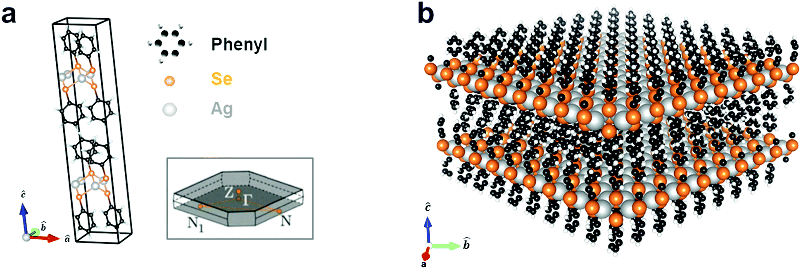 | ||
| Fig. 1 Silver benzeneselenolate ([AgSePh]∞) unit cell and molecular structure. (a) Primitive cell and first Brillouin zone (inset); see ESI† for cell coordinates. (b) Extended layered molecular structure of [AgSePh]∞ consisting of 2D sheets of AgSe spaced by phenyl groups. | ||
We measure the optical properties of [AgSePh]∞ thin films which were synthesized following a similar chemical route as recently reported for non-luminescent lamellar silver organo-thiolate crystals.22–24 This scalable method yielded nano-crystalline (NC), continuous, and optically semi-transparent films (Fig. 2a and b), which enable ultrafast spectroscopy with a minimal background from scattering. We confirm the morphology and the crystallinity of the films by scanning electron microscopy (SEM) and by grazing-incidence wide-angle X-ray scattering (GIWAXS) (Fig. 2a inset and Fig. 2b). The 70 nm thick [AgSePh]∞ film shows three distinct optical absorption resonances at X1 = 2.67 eV, X2 = 2.74 eV and X3 = 2.86 eV (Fig. 2c and Fig. S1, ESI†), while the photoluminescence (PL) spectrum exhibits a single peak centred at X1 = 2.66 eV. The sharp peaks at the onset of the measured linear absorbance spectrum are consistent with bound excitons.
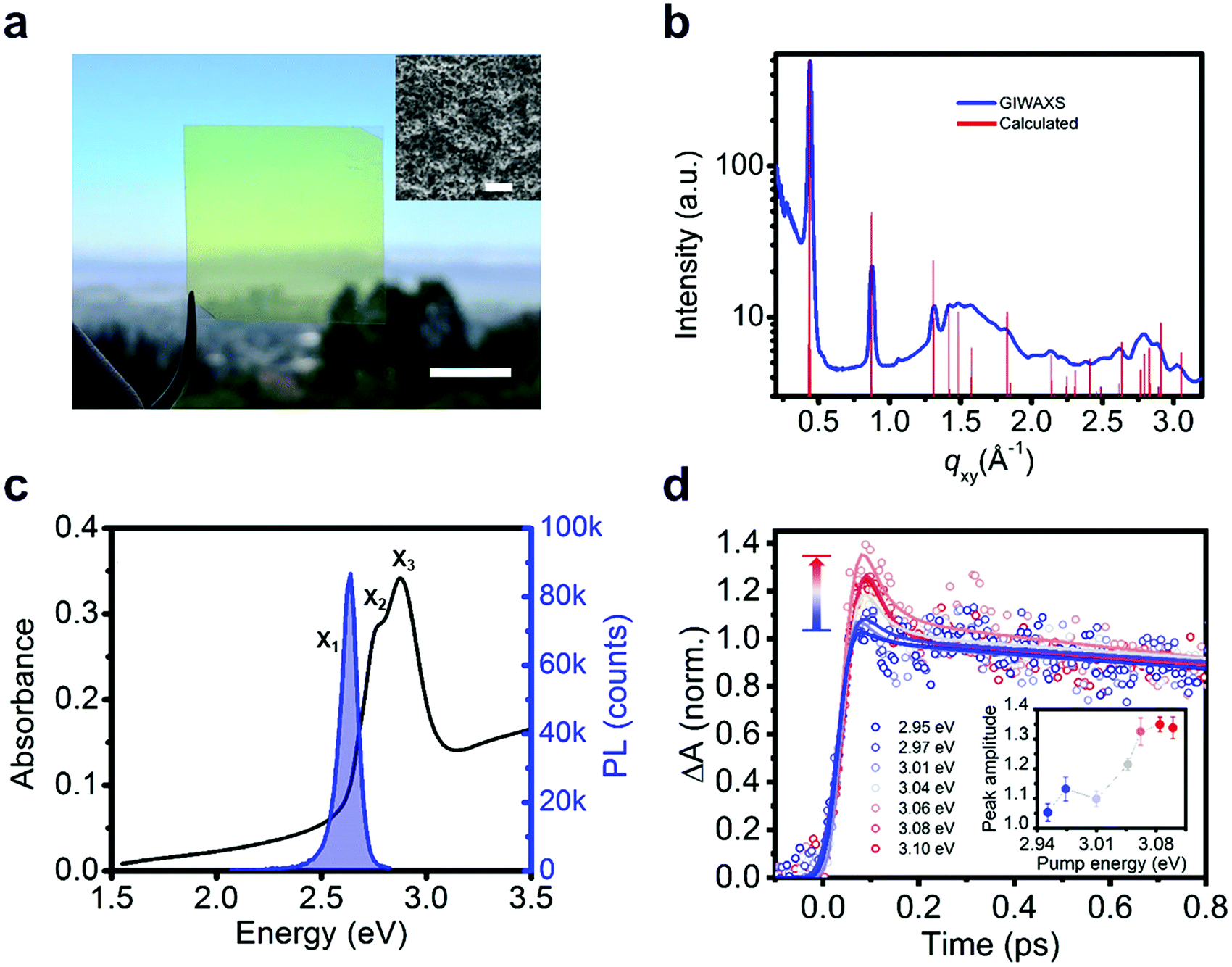 | ||
| Fig. 2 Experimental realization of [AgSePh]∞ films, characterized by distinctive crystalline and opto-electronic properties. (a) Photograph (scale bar, 1 cm) and SEM micrograph (inset, scale bar, 500 nm) of a continuous, nano-crystalline [AgSePh]∞ film. (b) Sample crystallinity revealed by GIWAXS (Grazing Incidence Wide Angle Scattering). Experimental GIWAXS spectrum (blue line) and calculated diffraction peaks (red lines). (c) Absorbance (black line) and photoluminescence (PL) spectra (blue line). The absorbance shows three excitonic resonances at X1 = 2.67 eV, X2 = 2.74 eV, and X3 = 2.86 eV. Photoluminescence emission occurs from a single peak at 2.66 eV corresponding to the lowest excitonic resonance X1. (d) Detection of band-edge absorption onset. Transient absorption spectroscopy reveals ultrafast relaxation (<150 fs decay) of free carriers by detuning the pump energy from 2.94 eV up to 3.08 eV. The traces probe the X2 excitons at 2.74 eV. Solid lines are fits to the data modelling the ultrafast thermalization. The inset shows the fitted amplitude of the initial thermalization vs. pump energy. | ||
The determination of the transport gap for [AgSePh]∞ is challenging, as the large absorption cross-sections of the excitons dominate the optical transitions, obscuring the band-edge absorption features. Therefore, we estimated the exciton binding energy using detuned transient absorption spectroscopy. Briefly, a nanocrystalline sample was pumped with narrowband pulsed light (<30 meV FWHM, in sub-saturation regime, see Fig. S2, ESI†) which was continuously tuned above the exciton resonances in steps of ∼30 meV while a broadband probe was used to monitor the initial temporal dynamics of the X2 exciton peak (Fig. 2d). At approximately Epump = 3.05 eV (0.38 eV detuning from X1) we observed a sharp onset of a sub-picosecond decay feature, whose amplitude increases approximately linearly with increasing detuning (inset of Fig. 2d and Fig. S3, ESI†). We ascribe this ultrafast decay to the initial dynamics of photoexcited free carriers. For large exciton binding energies (∼100 meV), free carriers at room temperature are approximately two times more efficient at inducing transient absorption.25,26 Furthermore, free carriers scatter efficiently among themselves, thermalize to the band edge, and form excitons within hundreds of femtoseconds, as reported in 2D transition metal dichalcogenides.17 The transient bleaching signal related to these carriers can therefore explain the observed sub-picosecond dynamics. For 2D WS2, Cunningham et al.17 showed that the linear increase of the ultrafast decay amplitude with increasing detuning is indeed consistent with the onset of the free carrier continuum. For smaller detuning, they additionally resolved a spectral plateau in the ultrafast decay related to higher excitonic Rydberg states. In our material system, with three overlapping excitonic resonances, we are not able to resolve such excited states within the experimental uncertainty. Therefore, we extract a lower bound for the experimental exciton binding energy at 0.38 eV.
Considering that the layered structure leads to high in-plane charge carrier confinement, a significant polarization anisotropy is expected for the excitonic optical transitions. To test this hypothesis, we use spectroscopic ellipsometry and back focal plane microscopy (BFP) to evaluate the degree of anisotropy in the NC films as summarized in Fig. 3. The best fit to the measured ellipsometry data is achieved with a film thickness of 40 nm (Fig. S4c and d, ESI†) and assuming uniaxial anisotropy, with indices in the in-plane (κ‖), and out-of-plane (κ⊥) directions (see fitting parameters in Tables S1–S4, ESI†). The extracted optical extinction coefficients from these fits are plotted in Fig. 3a. The observation of anisotropy, despite the polycrystalline nature of the measured area, is due to a strong (002) preferential orientation of the crystalline domains of the film as seen in GIWAXS (see Fig. S5, ESI†): a majority of the crystallites are oriented such that their layers lie flat on the surface. The extinction coefficient in the in-plane direction κ‖ is clearly larger in magnitude, indicating that the in-plane exciton transition dipole moments ![[small mu, Greek, circumflex]](https://www.rsc.org/images/entities/i_char_e0b3.gif) ‖ have higher strength (see Methods) than the out-of-plane ones ⊥ (see schematic in Fig. 3b). Consequently, we also expect the PL (from X1) to have a preferential in-plane polarization. To explore anisotropy at the level of single crystalline domains, BFP imaging is employed, which has revealed similar anisotropy in layered materials.27 However, the domain size in the nanocrystalline film is too small to resolve individual domains, so a second synthetic protocol (see Methods) was developed to produce larger crystalline domains oriented parallel to the substrate, enabling these critical microscopic, single-crystal polarization anisotropy measurements (Fig. 3b; and XRD data in Fig. S6, ESI†). We verify that the NC films and the single crystals exhibit quantitatively matching excitonic absorption by determining the absorption coefficient via micro-absorption and thickness calibration by AFM (Fig. S4 and S7, ESI†). Notably, however, the PL intensity of the microcrystals is ∼20× higher than that of a NC film with the same thickness (Fig. S8, ESI†). This increased brightness of the microcrystals indicates that the NC film suffers from many more non-radiative recombination centres, resulting in a lower quantum yield.
‖ have higher strength (see Methods) than the out-of-plane ones ⊥ (see schematic in Fig. 3b). Consequently, we also expect the PL (from X1) to have a preferential in-plane polarization. To explore anisotropy at the level of single crystalline domains, BFP imaging is employed, which has revealed similar anisotropy in layered materials.27 However, the domain size in the nanocrystalline film is too small to resolve individual domains, so a second synthetic protocol (see Methods) was developed to produce larger crystalline domains oriented parallel to the substrate, enabling these critical microscopic, single-crystal polarization anisotropy measurements (Fig. 3b; and XRD data in Fig. S6, ESI†). We verify that the NC films and the single crystals exhibit quantitatively matching excitonic absorption by determining the absorption coefficient via micro-absorption and thickness calibration by AFM (Fig. S4 and S7, ESI†). Notably, however, the PL intensity of the microcrystals is ∼20× higher than that of a NC film with the same thickness (Fig. S8, ESI†). This increased brightness of the microcrystals indicates that the NC film suffers from many more non-radiative recombination centres, resulting in a lower quantum yield.
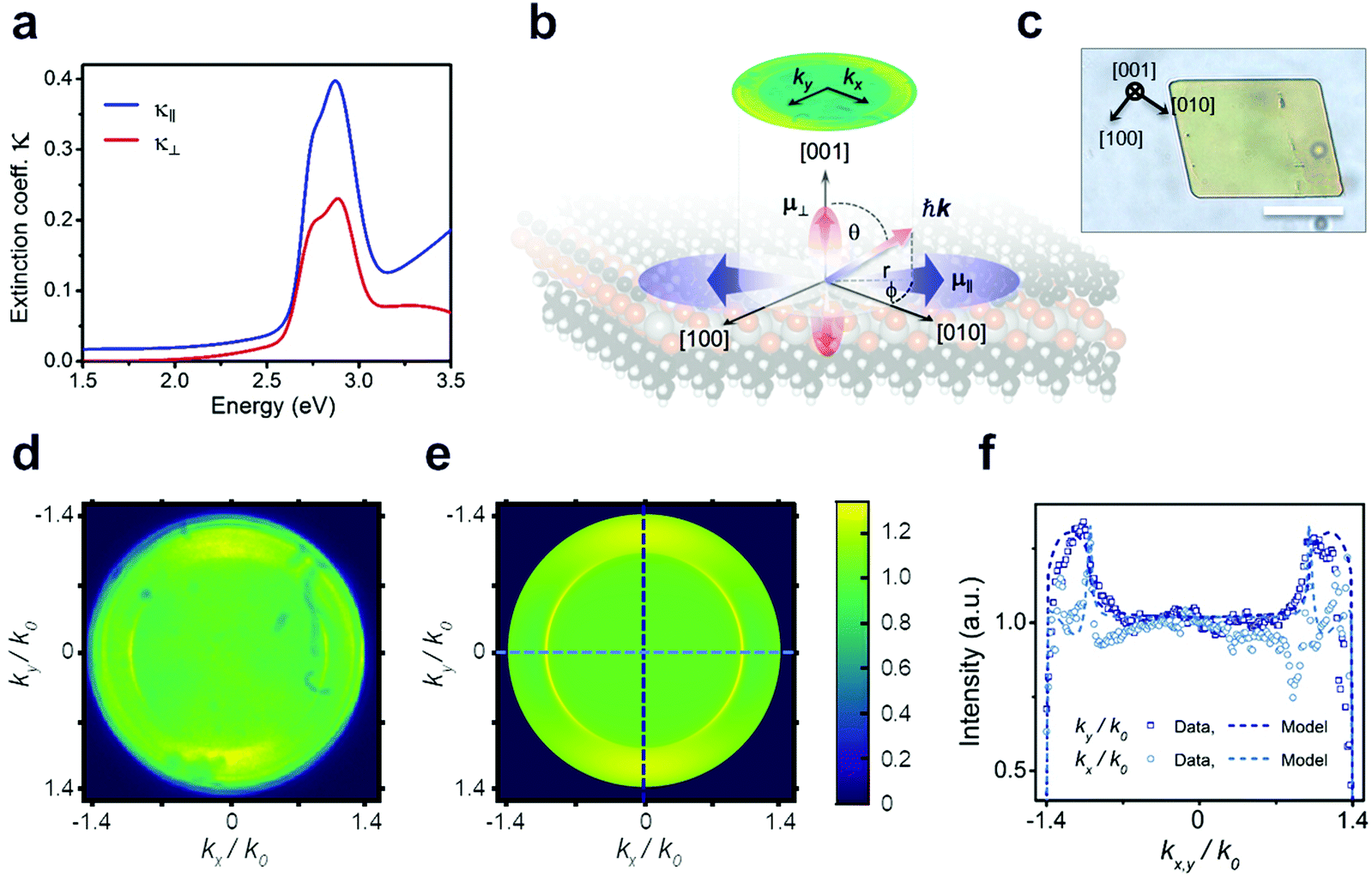 | ||
| Fig. 3 Experimental assessment of the in-plane ‖ and the out-of- plane ⊥ excitonic dipole moments. (a) Optical extinction coefficient κ for the in-plane κ‖ and out-of-plane κ⊥ components, calculated from ellipsometry fit indicating a strong anisotropy. (b) Schematic of exciton transition dipole orientation within the crystal derived from ellipsometry and PL experiments; projection of the PL photon momentum onto the Fourier plane as detected by back focal plane imaging (BFP). (c) Optical image of the micron-size single crystal. Scale bar, 20 μm. (d)–(f) BFP image and modelling of single crystal PL directionality. Experimental (d) and modelled (e) back focal plane image for the emission from a single crystal through a linear polariser aligned with the [010] axis. The ‖ strength is 1.7× higher on average than the ⊥ strength, as described by the modelling of the horizontal (light blue) and vertical (dark blue) cross sections (f). | ||
Fig. 3d–f summarizes microscopic BFP measurements of a single crystallite of [AgSePh]∞. BFP measures the angular distribution of PL emission from the sample. By modelling the resulting PL emission pattern (or image), it is possible to reconstruct the in-plane vs. out-of-plane emission components (see Fig. S9–S12 and Methods for details, ESI†). Fig. 3d and e shows the experimental and calculated BFP signals when passed through a linear polariser aligned with the [010] axis (kx). We obtain the correlation between microscale morphology and crystal lattice orientation by TEM diffraction (Fig. S15, ESI†). Theoretical BFP signals are generated by using experimental n, κ data from ellipsometry measurements and subsequently fit to the measured BFP profiles. This fitting was done for polarised and unpolarised BFP signals to determine the relative transition dipole strengths associated with each exciton along the three axes. BFP modelling shows that the horizontal transition dipole, restricted to the preferential orientation [010], is on average 1.7× larger than the out-of-plane transition dipole ⊥. Additionally, the strength of [010] is 2.4× higher than [100] (see Fig. S13 and S14, ESI†).
To confirm this optical response, we performed linearly polarised micro-absorption spectroscopy on a single crystal (see Methods). An absorption spectrum was recorded for each polarization orientation of the broadband illumination, as summarized in Fig. 4a. By rotating the polarization, different excitons were stimulated. The data was fit with three Gaussian peaks on top of a background (Fig. S16, ESI†), and the absorption intensity for each excitonic band is plotted in polar coordinates onto the real space optical image of the measured crystal (Fig. 4b). From this picture, it is apparent that the X1 and X3 transition dipole moments contribute to [010], while X2 contributes to [100], which is orthogonal to the other two. We can now define a polarization anisotropy as the ratio of the absorption along [010] and [100] extracted from the polar plot in Fig. 4b. Then, the degrees of polarization anisotropy for the X1 and X2 transition dipoles lie around 90%. We therefore confirmed that the in-plane exciton transition dipole moments ‖ = [100] + [010] preferentially align along the high symmetry crystal directions, resulting in two spatially orthogonal excitons with different energies. Given this large absorption anisotropy, we investigated the PL radiated by [010] at the energy associated with X1.
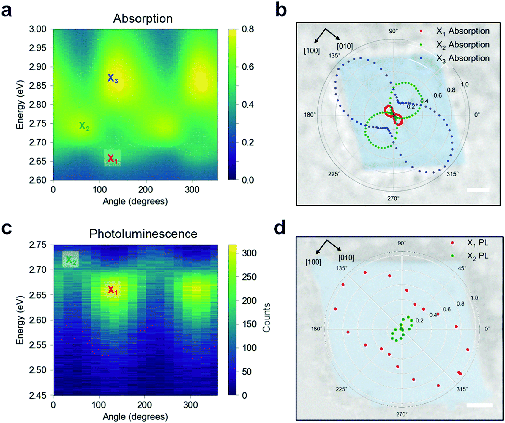 | ||
| Fig. 4 The in-plane anisotropy of the energy-resolved dipole moments. Angle-resolved absorption spectra (a) and PL spectra (c) for different linear polarizations of the incident light (a) and emitted light (c) are shown. Excitons X1 and X3 contribute to [010] while X2 contributes to the orthogonal [100]. PL was only detectable from X1 and X2 in our system. The fitted intensities of the absorption peaks (b) and PL peaks (d) are plotted in polar coordinates and overlaid to the measured crystal to give spatial coordinate reference. Scale bars, 5 μm. | ||
When the single crystal is pumped with monochromatic circularly polarised laser pulses, two linearly polarised PL peaks emerge (Fig. 4c), corresponding to the energies of X1 and X2 states that were observed via absorption measurements. The normalized Gaussian intensity (see Fig. S17, ESI†) is plotted in polar coordinates on top of the measured crystal (Fig. 4d) to highlight the PL polarization with respect to the crystal orientation. These results suggest that the PL emission maintains the polarization acquired in the absorption event, and consequently, that the orthogonal polarization of the excitons prevents efficient thermalization from the excited state X2 to the lowest-energy state (X1). Moreover, the anisotropic nature of these low-lying excitons is consistent with our ab initio calculations, as we discuss below. Polarization resolved micro-PL imaging reveals that the PL polarization is uniform over the entire crystal, indicating a long-range order of the in-plane crystallinity (Fig. S18a and b, ESI†). We note that thinner crystals seemingly have higher PL anisotropy (Fig. S18c and d, ESI†), suggesting a more disordered structure for thick crystals along the out-of-plane direction.
Our GW and Bethe–Salpeter equation (BSE) calculations of pristine crystalline [AgSePh]∞ confirm the trends measured here, and they provide more detailed information on the origin of the low-lying excitations and observed photophysics (see Methods and Table S5 for computational details, ESI†). Our calculations predict that [AgSePh]∞ is a direct-gap semiconductor with a relatively large band dispersion (Fig. 5a), and a transport gap of 2.7 eV at the Γ point. This value is consistent with but somewhat lower than (by ∼0.3 eV) that extracted from measurements, a modest discrepancy that we attribute to a combination of two factors: the limitations of the specific one-shot G0W0 computational approach used here (see Methods), and structural differences between the ideal pristine structure used for the calculations and the sample used for the measurements, since the latter may exhibit some degree of disorder. The electronic structure at the valence and conduction band edges is dominated by contributions from the AgSe layers, principally Ag 4d and Se 3p; the conduction band minimum additionally features Ag 5s character (Fig. 5a). The phenyl π and π* states are largely grouped at energies well below and above the Ag- and Se-rich valence and conduction band edges, respectively, consistent with the relatively large benzene gap and minimal carbon character at Γ (see ESI,† Fig. S19); however, notably, the π and π* states dominate the band character at N.
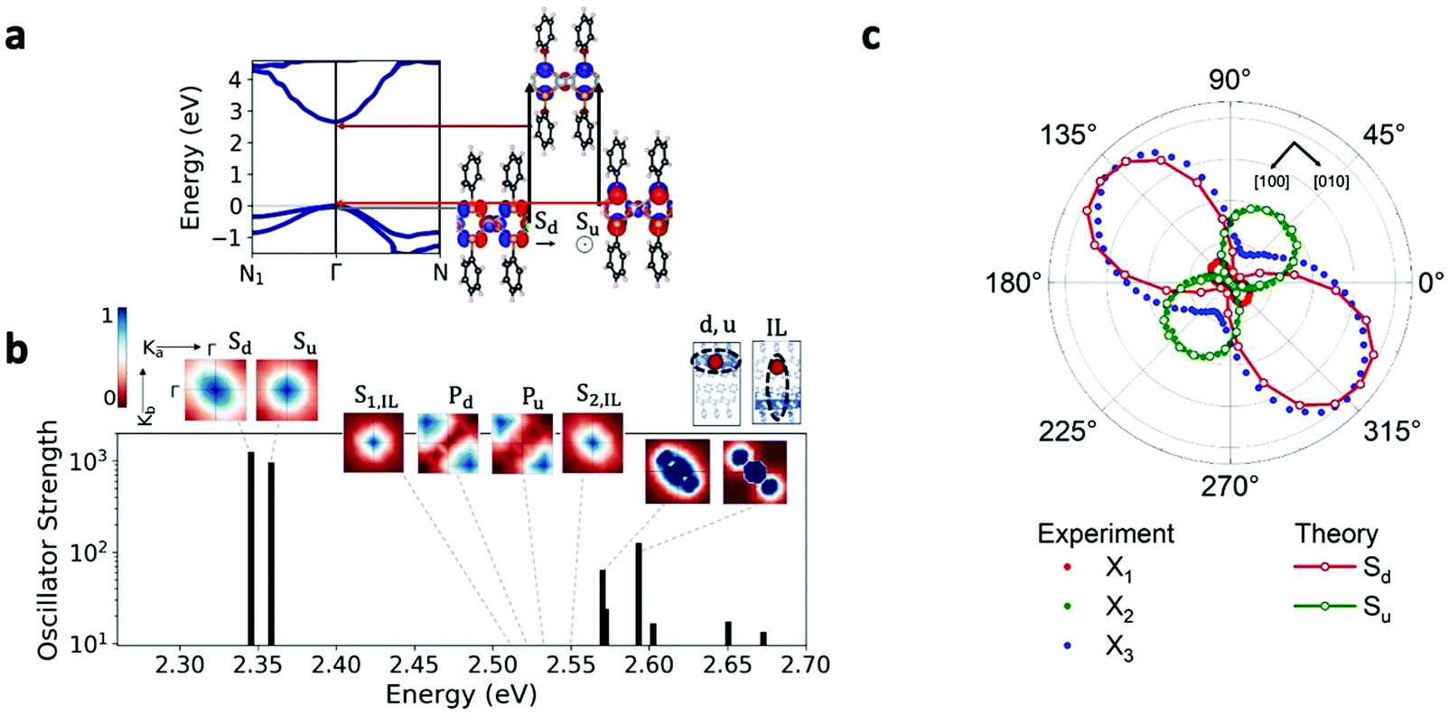 | ||
| Fig. 5 (a) Calculated GW band structure of [AgSePh]∞. We find a direct gap of 2.7 eV at Γ. Isosurfaces of the wavefunctions at valence and conduction band edges at Γ are shown. The single-particle transitions that dominate the lowest two exciton states, Sd and Su, are demonstrated with arrows. (b) Calculated GW-BSE excitation spectrum of [AgSePh]∞. Black lines represent the excitation energies in the presented energy range, with oscillator strengths presented on a logarithmic scale. Isosurfaces of exciton wavefunctions are shown in k-space in crystal coordinates, where blue (red) represents large (small) exciton coefficients. Su,d and Pu,d represent s-like and p-like intralayer excitations, dominated by transitions involving the upper (u) and lower (d) valence band states at Γ. SIL represents interlayer excitons. Real-space representations of the envelope wavefunction distributions for representative intralayer (u,d) and interlayer excitons are also presented for a fixed hole position (marked with a red circle). (c) Angle-resolved absorption spectra, comparing the measured absorption (normalized to the highest intensity peak) of the three measured excitons (dots) with the GW-BSE absorption intensities of the computed low-energy excitons (solid lines-open dots). | ||
Consistent with experiment, we find from our ab initio GW-BSE calculations that this band structure gives rise to a diversity of low-lying bound excitons (Fig. 5b). Our predicted lowest-lying excitation energy is approximately 350 meV less than our computed gap, in quantitative agreement with the exciton binding energies obtained from our detuned transient absorption spectroscopy measurements. Also consistent with experiment, the two lowest excitons from our calculations, Sd and Su, are strongly confined to the AgSe planes, consistent with the orbital character of band edges: regions of high electron probability are localized around the hole within the same layer (for fixed hole position, Fig. 5b). The states Sd and Su have different in-plane symmetry, which arises from their constituent transitions, involving one or the other of two nearly-degenerate valence band edge (or hole) states with different orbital contributions (see Fig. 5a). The excitonic picture of the Γ–Γ transitions follows a quasi-2D model, similarly to the case of layered GaSe, as previously published.28 Further corroborating our measurements, we find that the absorption of the two lowest bright excitons, Sd and Su, shows a marked dependence on the in-plane light polarization direction, as shown in Fig. 5c and in Fig. S19 (ESI†). For these excitons, the largest computed intensity is for polarization directions aligned along the Ag–Ag and the Se–Se rows, corresponding to the [010] and the [100] crystallographic directions, respectively, of the conventional unit cell used to reference the measurements (see Methods, Fig. 5a and Table S5 in the ESI†). The polarization dependence is in good agreement with experiment, as shown in Fig. 5c. Notably, the relative absorption strength between the two excitons suggests that the two lowest-energy GW-BSE excitons correspond best to the X3 and X2 excitons observed in experiment, respectively. In sum, our results confirm the anisotropic nature of optically active intralayer excitons, in good correspondence with the experimental observations. This anisotropy is a result of the nature of the single-particle valence states dominating the transitions making up the exciton states, and these are hence a direct result of the intrinsic layer structure and the unit cell symmetry.
While the inner-layer structural composition explains the origin of exciton anisotropy, we note that the measured photophysics will reflect any disorder effects present in the [AgSePh]∞ system. Such disorder can for example be due to broken symmetry in the sample caused by relative rotations of the phenyl rings.20 This hypothesis is supported by TEM electron diffraction experiments (see Fig. S15, ESI†) showing a lack of long-range order in the packing of the phenyl rings in the majority of crystals, while only small areas display signature characteristics of herringbone or parallel ordering of the ligands. Such effects are not captured by our GW-BSE calculations, which are necessarily performed assuming an ordered sample. Still, our calculations confirm the primary photophysical features of this hybrid layered system, including the direct gap semiconducting behaviour, and a multiplicity of strongly-bound excitons confined to the AgSe planes with differing in-plane anisotropy. These rationalize our optical measurements and the preferable directionality of the absorption and emission spectra, and, by identifying the specific orbital character of these transitions, point toward routes of potential tunability of these excitations in this class of layered systems.
Building on past calculations,29–31 our results are broadly consistent with prior work on related classes of hybrid and low-dimensional materials, layered halide perovskites11 and of 2D transition metal chalcogenide semiconductors, where model calculations9,10 have provided a detailed framework for understanding measurements of strongly-bound and confined excitons. Our ab initio GW-BSE calculations capture the inhomogeneous and anisotropic nature of the optical absorption, dielectric screening, and electron–hole interaction in this complex layered hybrid material, yielding good agreement with experiment, without resorting to simplifications or empirical approximations, paving the way for future ab initio GW-BSE work on hybrid chalcogenide systems like [AgSePh]∞, layered perovskite systems, and beyond.
Finally, we consider the possibility of substituting the chalcogen atoms in the lattice structure to tune the excitonic resonance. Following a similar synthetic method to the one used for [AgSPh]∞, we obtain [AgSPh]∞ and [AgTePh]∞ compounds (see Fig. S20 for XRD data, ESI†). Fig. 6 illustrates the comparison of the optical response for the three representatives of the silver benzene chalcogenide family. The thiolate polymer shows an excitonic absorption resonance in the near UV, but no luminescence can be observed, while the tellurate polymer has split excitonic peaks that give rise to a red-shifted PL compared to the [AgSePh]∞ (Fig. 6b). A deeper analysis of the excitonic behaviour in the thiolate and tellurate compound is beyond the scope of this work. Nevertheless, these optical spectra show great potential for absorption/emission tunability in this material platform, which can be controlled by a facile wet-chemistry approach.
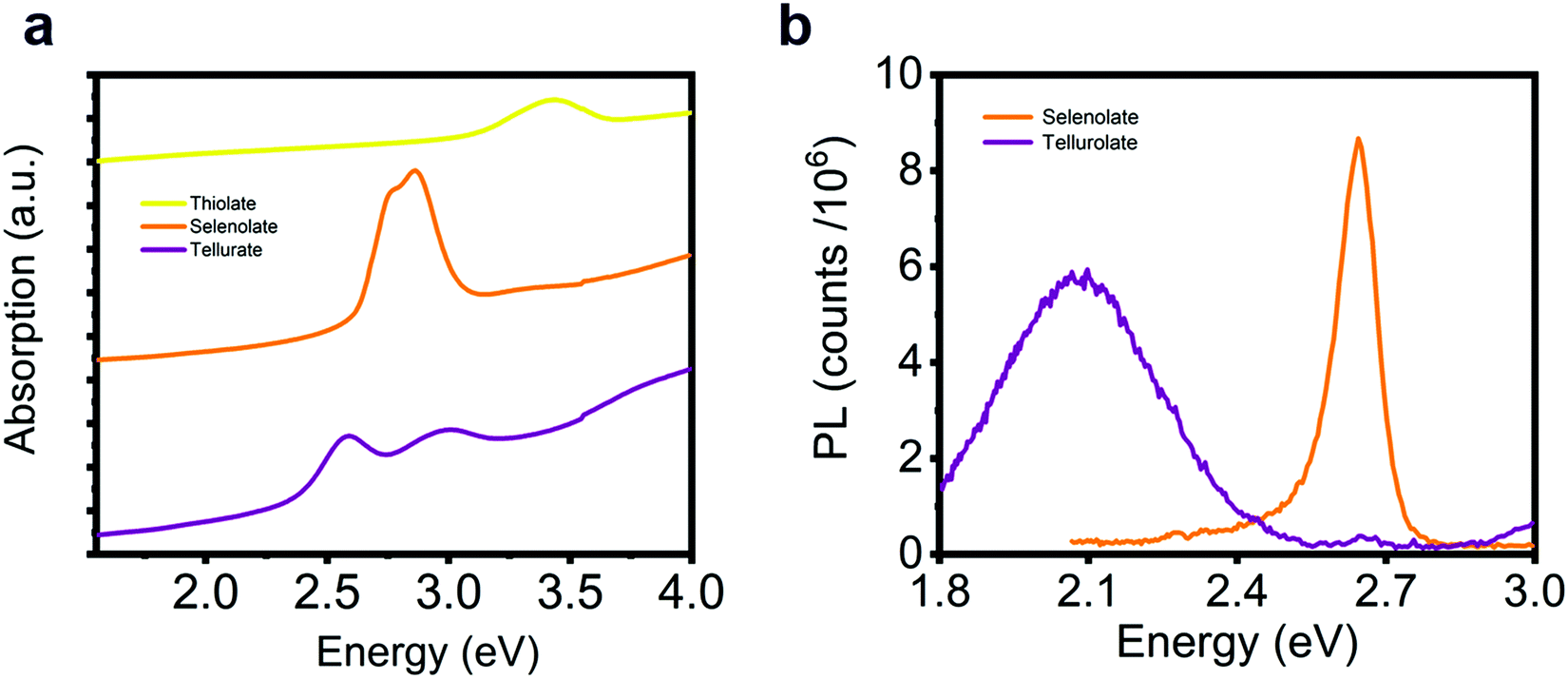 | ||
| Fig. 6 Optical properties of the different silver benzene chalcogenide compounds. (a) The excitonic properties are heavily modulated by the chalcogen in the lattice. The lighter the chalcogen, the higher is the energy of the optical transition seen in absorbance. (b) While the [AgSPh]∞ does not show PL, the [AgTePh]∞ shows a broad PL peak significantly red-shifted compared to the [AgSePh]∞. | ||
In conclusion, we introduce a new tuneable material platform that significantly impacts the study of room-temperature excitonic properties in hybrid systems, beyond 2D perovskites. The inorganic covalent layers made of transition metal chalcogenides provide effective quantum confinement while the low dielectric constant of the organic groups leads to high exciton binding energy. Our calculations predict that its low-lying excitons have varying symmetries, as well as mixed intralayer and interlayer nature. In-depth spectroscopy of the optical absorption and emission characteristics demonstrates a strong orientation of the exciton transition dipole moments along high-symmetry crystal directions. This study significantly advances our understanding of hybrid QW materials and can serve as reference for the investigation of these classes of materials. Furthermore, this material class is amenable to chemical tunability that impacts its photo-absorption/emission, while at the same time preserving the confined nature of the electronic excitations. Finally, since the synthesis used for preparing the NC thin film is fast and easily scalable, we anticipate potential applications in a broad class of low-cost air-stable optoelectronic devices.
Materials and methods
Synthetic procedure
[AgXPh]∞ (X = S, Se) nano-crystalline film: 10 nm thick silver films thermally evaporated on fused silica substrates were exposed to UV ozone for 10 min to oxidize silver. Subsequently, the oxidized silver films were reacted. According to the used chalcogen different procedures were employed: 1. With benzeneselenol for [AgSePh]∞ by vapour transport for 2 hours in an oven at 80 °C. 2. With thiophenol for [AgSPh]∞ by vapour transport overnight in an oven at 80 °C. 3. All the samples were rinsed in isopropyl alcohol (IPA) to remove the unreacted organo-chalcogen reagent and N2 dried. [AgSePh]∞ micro-crystalline sample: 10 nm thick silver films were thermally evaporated on fused silica (or directly on TEM grids for diffraction experiments). Subsequently, the silver films were reacted with benzeneselenol by vapour transport for 4 days in an oven at 80 °C. The sample was rinsed in IPA to remove the unreacted benzeneselenol and N2 dried. [AgTePh]∞ micro-crystalline sample: 10 nm thick silver films were thermally evaporated on fused silica. The silver film (without ozone treatment) was reacted with diphenyl ditelluride to obtain [AgTePh]∞ by vapour transport overnight in an oven at 80 °C. The sample was rinsed in IPA to remove the unreacted benzeneselenol and N2 dried.Morphological and structural characterization
GIWAXS measurements were performed at the Advanced Light Source beamline 7.3.3 at Lawrence Berkeley National Laboratory,32 with the bend beamline operated at an energy of 10 keV, a beam size of 0.5 mm, and a 280 mm sample-detector distance. Measurements were performed in a helium atmosphere on a grazing incidence static stage. 2-Dimensional images were collected using CCD area detectors having a 172 μm pixel size. The patterns collected were calibrated using a standard silver behenate powder sample.33 2D data reduction was performed using the Nika 2D data reduction package34 (Advanced Photon Source, Argonne National Laboratory) for Igor Pro (Wavemetrics Inc.), and Ewald Sphere corrections were performed using Xi-cam.35P-XRD area images were recorded in air on a Bruker Gadds-8 diffractometer with Co Kα source operating at 35 kV and 40 mA. Scanning electron microscopy (SEM) images were collected on a Zeiss Gemini Ultra-55 Analytical Field Emission SEM with a secondary electron detector and at an accelerating voltage of 3 keV.
Transient absorption spectroscopy
We use an ultrafast transient absorption system with a tuneable pump and white-light probe to measure the extinction of excitonic transitions as a function of pump–probe delay time and probe wavelength. The laser system consists of a regeneratively amplified Ti:sapphire oscillator (Coherent Libra), which delivers 4 mJ pulse energies centred at 800 nm with a 1 kHz repetition rate. The pulse duration of the amplified pulse is approximately 50 fs. The laser output is split by an optical wedge to produce the pump and probe beams and the pump beam wavelength is tuned using a Coherent OPerA optical parametric amplifier. The probe beam is focused onto a sapphire plate to generate a white-light continuum probe. The time-resolved differential extinction spectra are collected with a commercial absorption spectrometer (Helios, Ultrafast Systems LLC). The temporal behaviour is monitored by increasing the path length of the probe pulse and delaying it with respect to the pump pulse with a linear translation stage (minimum step size 16 fs).Ellipsometry
Uniform and continuous NC thin films over the spot size of the measurement (3 mm in diameter at normal incidence) were measured using a J. A. Woollam M-2000 spectroscopic ellipsometer. In addition to standard ellipsometry data collected at 5 degree increments between 45 and 75 degrees off normal incidence, transmission, reflection, and depolarization spectra were also collected and used in the fitting (J. A. Woollam CompleteEASE software package). The best fit was arrived at assuming uniaxial anisotropy, with two B-Spline layers representing the ordinary (out-of-plane) and extraordinary (in-plane) contributions. The B-Spline layers were then parameterized with a series of Gaussian lineshapes to encompass the observed excitonic and band edge-like features (see Tables S1–S4 for parameters values, ESI†). Three Gaussians corresponding to excitons were fixed at 2.67, 2.74, and 2.86 eV in concordance with peak positions seen in absorption and photoluminescence spectroscopy.Back focal plane microscopy
Individual crystals are imaged using a homebuilt inverted microscope with an oil immersion objective (Nikon Plan Apo VC, 100×, NA = 1.4; oil: Cargille Immersion Oil Type FF, n = 1.479, Lot: 010780), tube lens (f = 200 mm), and EMCCD camera (Andor iXon Ultra 897 EMCCD, T = −60 °C). The samples are excited by a 405 nm CW diode laser (Thorlabs LP405-SF30) and their fluorescence (emission ∼465 nm) is collected (maximum collection angle ∼70°), passed through a dichroic mirror (Semrock FF414-Di01-25 × 36) and additional long-pass and bandpass filters to reduce background signal (Semrock FF02-409/LP-25, Thorlabs FB450-40). A Bertrand lens (f = 200 mm) is inserted between the objective and tube lens to image the back focal plane, or Fourier space. Exposure time: 2–3 s, readout rate: 3 MHz, EM gain disabled. Polarised BFP images are taken by inserting a polariser in the emission pathway (see Fig. S10, ESI†).Transmission electron microscopy (TEM)
TEM was performed using a JEOL 2100F electron microscope operated at an accelerating voltage of 120 kV and a reduced dose rate of approximately 10 e− nm−2. The acceleration voltage and dose rate were chosen to minimize sample beam damage. The microscope was operated in STEM mode for imaging using a High-Angle Annular Dark Field (HAADF) detector. Spatially resolved nano-beam diffraction (NBD) patterns were acquired in scanning mode by defocusing the STEM probe into a parallel beam of approx. 80 nm diameter using the condenser lens system and moving the beam to a position of interest. The resulting diffraction patterns were captured using a 16 bit Gatan Ultrascan 1000 camera with exposure times ranging from 0.1 s to 2.0 s corresponding to 1–20 e− nm−2 electron dose.AFM
Topography maps of nano-crystalline thin films and micro-crystallites were collected in non-contact mode using a Bruker Icon AFM with a BudgetSensors TAP150Al-G probe. Post processing was performed using Gwyddion to level the data and to extract line profiles for thickness determination.Micro-absorption microscopy/spectroscopy
The samples comprised of single crystallites on transparent glass slides were mounted on an inverted microscope (Nikon). From the backside of the substrate, the samples were illuminated with a collimated broadband light from a halogen lamp (Nikon). Transmitted light through the sample was collected with a 40× 0.60 NA objective (Nikon) and spatially filtered in the image plane of the microscope by a 100 μm diameter pinhole to provide a spatial resolution of ∼2.5 μm. The spatially resolved transmitted light was dispersed with imaging spectrograph (Acton, SpectraPro 2300i) and imaged on a liquid N2-cooled charge coupled device (CCD) camera (Princeton Instruments, SPEC-10). The polarization state of the broadband illumination was controlled by inserting a polarising film (Thorlabs) into the illumination path and systematically rotating its orientation from 0° to 360°. Absorption of the single crystallites was calculated by computing the normalized difference between the spectrum of the transmitted light through the crystallites on the substrate and the spectrum of the transmitted light through the substrate alone. Thick glass substrates (1 mm) were used to minimize substrate-related interference effects in the measurement.Micro-photoluminescence microscopy/spectroscopy
Samples composed of micron-sized crystals were loaded on an inverted scanning confocal microscope (Nikon). Circularly polarised pulsed laser excitation (λ = 450 nm; 140 fs pulse width; 80 MHz repetition rate) was focused to a diffraction-limited spot by a 40× 0.60 NA objective (Nikon). Emission from the sample was collected by the same objective and laser light was filtered by long-pass interference filters (Semrock, HQ450LP). The collected and filtered emission from the sample was additionally passed through a high-quality polariser (Thorlabs) and dispersed and analysed by a cooled scientific CCD camera (Andor, iXon 897) attached to an imaging spectrograph (Acton SpectraPro 2300i). To analyse the polarization state of the emitted light, emission spectra were collected at different orientations of the polarization filter which was rotated from 0°–360°. Care was taken to calibrate for the polarization responses of the microscope collection optics and detectors by performing the same measurements with unpolarised broadband light, but it was found that only negligible corrections were needed. The data were fitted with sets of Gaussian peaks (Fig. S16, ESI†).Back focal plane modelling
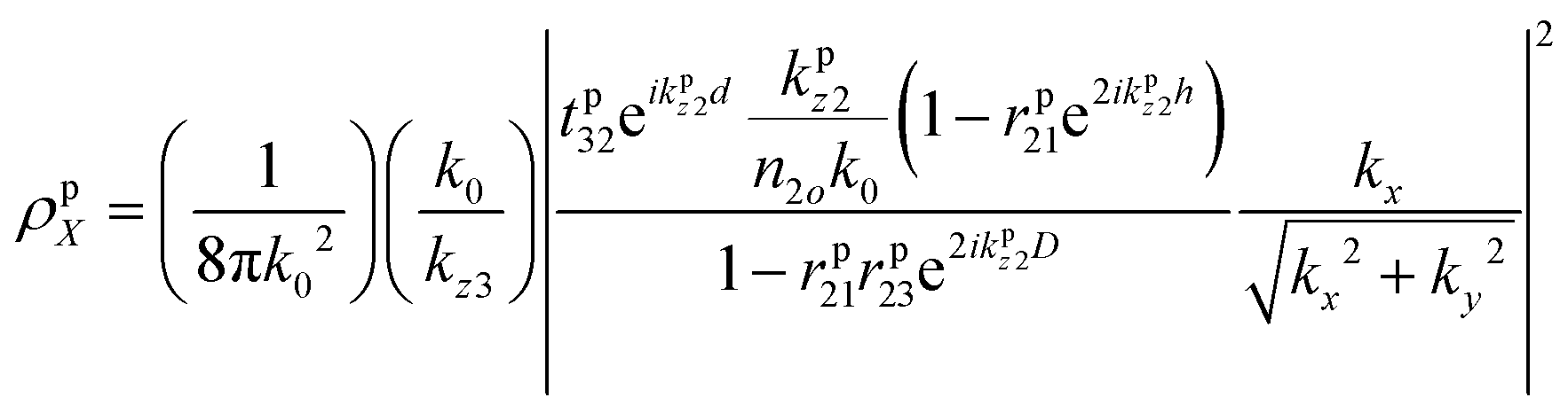
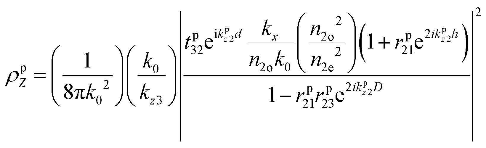
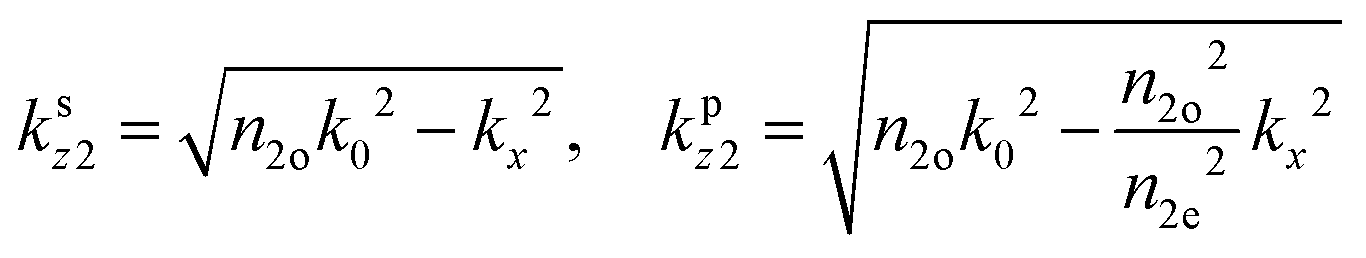
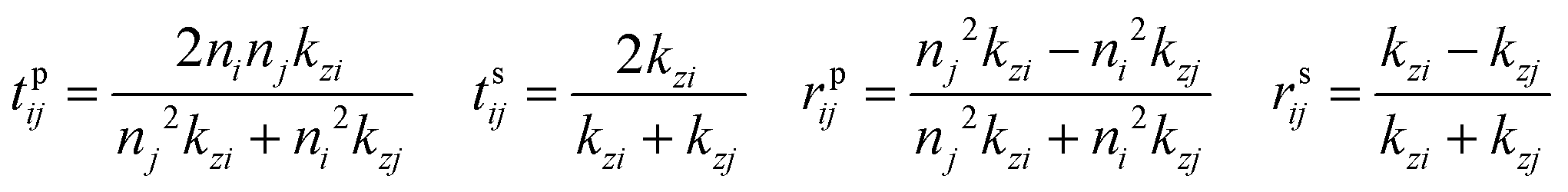
The modelled back focal plane (BFP) images are generated using the analytical formulas described by Schuller, et al.27 and Gao, et al.36 Here we use the formulas for a dipole emitting from a thin film when a polariser is aligned in the direction of X, as shown in Fig. S9 (ESI†). Because of the polariser, we only observe in-plane dipoles in the X direction and the kx component of out-of-plane dipoles (Z).36 To describe the BFP image without a polariser, one must add contribution from dipoles aligned with the Y axis and the ky component of dipoles aligned along the Z axis. The calculated emission (NPOL) projected on the imaging plane (in kx, ky) when using a polariser is:NPOL(kx,ky) = C(ρsX![[n with combining macron]](https://www.rsc.org/images/entities/i_char_006e_0304.gif) X|μX|2 + ρpXX|μX|2 + ρpZZ|μZ|2) X|μX|2 + ρpXX|μX|2 + ρpZZ|μZ|2) | (1) |
is the dipole distribution, and μ is the dipole moment. The quantity of i|μi|2 is referred to as the “dipole strength.” For a dipole emitting from a thin film with ordinary (IP) and extraordinary (OP) refractive index n2o and n2e, the LDOS can be described as: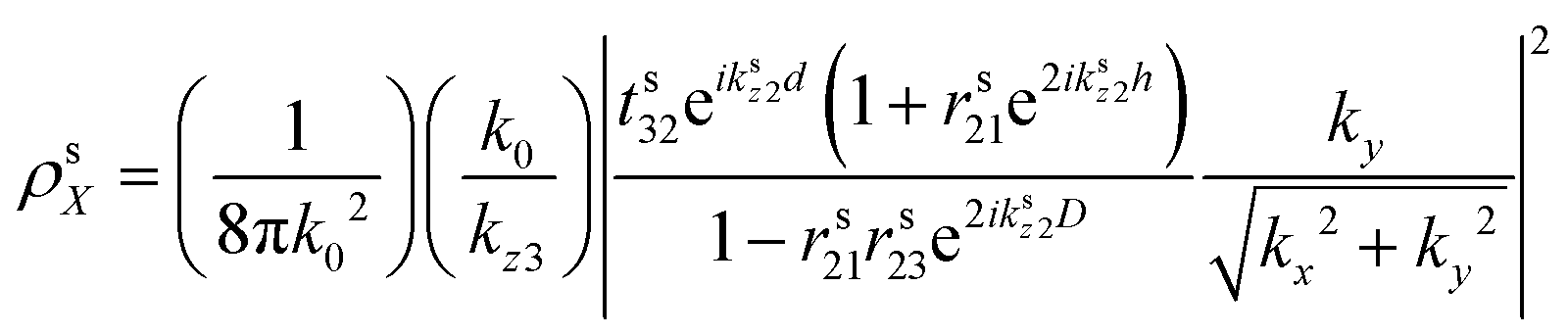 | (2) |
 | (3) |
 | (4) |
 | (5) |
 | (6) |
Note: n2o is used for n2 in the Fresnel coefficient equations. These equations describe the dipole emission from a specific position (h from the substrate) within the thin film (where D = d + h). Therefore, to adequately describe emission from the thin film, one calculates the dipole emission for every incremental h within the thin film and sums them to determine the total emission pattern. We found a step size of 1 nm to be sufficient.
In each crystal measured with back focal plane imaging, we fit the thickness of the crystal and the ratios of the dipole strengths along the three Cartesian axes. First, we fit the polarised back focal plane images, where the polariser is aligned along the [010] axis of the crystal. Using a polariser removes the light emitted by dipoles aligned along the [100] axis, reducing the number of fitted parameters. We generate modelled BFP images as discussed in the previous section for a series of thicknesses and dipole strengths. The crystals are known to be around 40 nm thick, so we generate back focal plane images ranging from 20–80 nm. Because we are working with normalized data sets, we consider a ratio of the dipole strengths (X|μX|2/Z|μZ|2) instead of the individual dipole strengths, reducing the number of unknowns.
We determine the best fit and error by calculating χ2, the sum of differences between the observed and expected values squared and divided by the expected values. We calculate χ2 for every data point where k < 1.25. The best fit occurs when χ2 is minimized, χmin2. Then, an error analysis was performed by following a procedure like that in ref. 37 and 38. In this procedure, one finds the values of the fitted parameters where χ2(Φ) − χmin2 = α, where Φ is a fitted value, such as thickness, and α is a constant for determining the confidence regions (see Table 1 of ref. 37). For the polarised data set, we are fitting two parameters, so we must find where χ2(Φ) − χmin2 = 2.30 in order to determine the error for one Sigma. Fig. S11 and S12 (ESI†) show the fitted values for crystal thickness and ratio of the in-plane (IP, [010] direction) to the out-of-plane (OP) dipole strength along with their corresponding errors, respectively. The in-plane ([010] direction) dipole strength is on average 1.9× stronger than the out-of-plane (OP) dipole strength.
Then, this process was repeated for the unpolarised images. The fitted parameters from the polarised images, crystal thickness, and in-plane to out-of-plane dipole strength were used to calculate the unpolarised BFP images. Thus, we only fit the dipole strength ratio for in-plane dipoles aligned along [010] to in-plane dipoles aligned along [100] in the unpolarised images. Fig. S13 (ESI†) shows an unpolarised BFP image, the corresponding model, and extracted profiles at kx and ky = 0 for comparison. Fig. S14 (ESI†) shows the fitted ratios of the dipole strengths of in-plane dipoles aligned along [010] to in-plane dipoles aligned along [100] along with their corresponding errors.
Computational methods
Density-functional theory (DFT)39 calculations are performed within the Perdew–Burke–Ernzerhof approximation (PBE)40 using the Quantum Espresso code.41 In our calculations, we start with the reported monoclinic C2/c structure of Cuthbert et al. (ref. 20). This structure has a degeneracy (and therefore partial occupations) associated with the phenyl orientations; we chose one of these orientations for our calculations. We transform the conventional cell reported in ref. 20 to a primitive cell, and optimize the internal atomic coordinates with DFT starting from the experimental values20 and using the vdW-DF2 functional42 (see Table S5 in the ESI† for the results of our calculations). We note the transformation matrix between primitive and conventional unit cells is [1/2 1/2 0]; [−1/2 1/2 0]; [001]. All crystallographic directions in this work are referenced to the conventional cell, following ref. 20. We use a 12 × 12 × 1 Monkhorst–Pack k-point grid, with a 70 Ry wave-function cut-off, within a plane-wave basis and using SG15 optimized norm-conserving pseudopotentials (http://www.quantum-simulation.org/potentials/sg15_oncv/), including the following valence states: Ag – 5s(1), 4d(10), 4p(6), 4s(2); Se – 4s(2), 4p(4), 3d(10). For quasiparticle excitations and band structure, we perform a one-shot G0W043 calculation from a PBE starting point, using the BerkeleyGW code44 within the generalized plasmon-pole model.43 We used a dielectric screening cut-off energy of 20 Ry, and 2000 bands. We have verified convergence of all parameters. For the optical excitations, we solve the Bethe–Salpeter equation (BSE),45 with the electron–hole interaction kernel evaluated on a 12 × 12 × 1 k-grid, and interpolated to a 36 × 36 × 1 k-grid to compute absorption spectra, including 4 occupied and 4 empty bands.Contributions
L. M., C. K., S. R. A., M. S. C., J. N. H., P. J. S., J. B. N. and A. M. S. conceived the project. S. R. A. and T. E. S. performed and analysed DFT and GW-BSE computations, under the supervision of J. B. N. L. M. and M. S. C. synthesized the samples. L. M. performed the optical spectrometry, and the X-ray diffraction. E. S. collected the GIWAXS data. L. M. and C. K. performed the transient absorption experiment. C. T. C. performed and analysed the ellipsometry experiment. C. T. C. performed the AFM experiment. C. E. and L. M. performed the back-focal-plane imaging and C. E. developed the fitting and interpreted the data. N. J. B., L. M. and M. S. conceived, performed and analysed the in-plane polarization study. E. S. B. took the PL maps. S. A. and B. S. recorded and analysed TEM diffraction data. L. M., S. R. A., C. K., C. E., C. T. C. N. J. B., J. B. N., and A. M. S. wrote the manuscript.Conflicts of interest
There are no conflicts to declare.Acknowledgements
Work at the Molecular Foundry was supported by the Office of Science, Office of Basic Energy Sciences, of the U.S. Department of Energy under Contract No. DE-AC02-05CH11231. This work was supported by the Center for Computational Study of Excited State Phenomena in Energy Materials, which is funded by the U.S. Department of Energy, Office of Science, Basic Energy Sciences, Materials Sciences and Engineering Division under Contract No. DE-AC02-05CH11231, as part of the Computational Materials Sciences Program, and using resources of the National Energy Research Scientific Computing Center (NERSC). S. R. A. acknowledges Rothschild and Fulbright fellowships. We thank Chenhui Zui and Alexander Liebman Palaez, staff members at beamline 7.3.3. of the Advanced Light Source Facility for their assistance in setting up the beamline for data acquisition and providing training.References
- A. Manchon, H. C. Koo, J. Nitta, S. M. Frolov and R. A. Duine, Nat. Mater., 2015, 14, 871 CrossRef CAS.
- K. J. Nash and D. J. Mowbray, J. Lumin., 1989, 44, 315–346 CrossRef CAS.
- F. Thouin, D. A. Valverde-Chávez, C. Quarti, D. Cortecchia, I. Bargigia, D. Beljonne, A. Petrozza, C. Silva and A. R. Srimath Kandada, Nat. Mater., 2019, 18, 349–356 CrossRef CAS.
- M. Kasha, Radiat. Res., 1963, 20, 55–70 CrossRef CAS.
- J. D. Plumhof, T. Stöferle, L. Mai, U. Scherf and R. F. Mahrt, Nat. Mater., 2013, 13, 247 CrossRef.
- M. H. Huang, S. Mao, H. Feick, H. Yan, Y. Wu, H. Kind, E. Weber, R. Russo and P. Yang, Science, 2001, 292, 1897 CrossRef CAS.
- A. Chernikov, T. C. Berkelbach, H. M. Hill, A. Rigosi, Y. Li, O. B. Aslan, D. R. Reichman, M. S. Hybertsen and T. F. Heinz, Phys. Rev. Lett., 2014, 113, 076802 CrossRef.
- K. Tanaka, F. Sano, T. Takahashi, T. Kondo, R. Ito and K. Ema, Solid State Commun., 2002, 122, 249–252 CrossRef CAS.
- J.-C. Blancon, A. V. Stier, H. Tsai, W. Nie, C. C. Stoumpos, B. Traoré, L. Pedesseau, M. Kepenekian, F. Katsutani, G. T. Noe, J. Kono, S. Tretiak, S. A. Crooker, C. Katan, M. G. Kanatzidis, J. J. Crochet, J. Even and A. D. Mohite, Nat. Commun., 2018, 9, 2254 CrossRef.
- Y. Cho and T. C. Berkelbach, J. Phys. Chem. Lett., 2019, 10, 6189–6196 CrossRef CAS.
- C. Katan, N. Mercier and J. Even, Chem. Rev., 2019, 119, 3140–3192 CrossRef CAS.
- D. H. Cao, C. C. Stoumpos, O. K. Farha, J. T. Hupp and M. G. Kanatzidis, J. Am. Chem. Soc., 2015, 137, 7843–7850 CrossRef CAS.
- B. Fluegel, Y. Zhang, A. Mascarenhas, X. Huang and J. Li, Phys. Rev. B: Condens. Matter Mater. Phys., 2004, 70, 205308 CrossRef.
- S. I. Stupp and L. C. Palmer, Chem. Mater., 2014, 26, 507–518 CrossRef CAS.
- D. B. Amabilino, D. K. Smith and J. W. Steed, Chem. Soc. Rev., 2017, 46, 2404–2420 RSC.
- E. A. Schriber, D. C. Popple, M. Yeung, M. A. Brady, S. A. Corlett and J. N. Hohman, ACS Appl. Nano Mater., 2018, 1, 3498–3508 CrossRef CAS.
- P. D. Cunningham, A. T. Hanbicki, K. M. McCreary and B. T. Jonker, ACS Nano, 2017, 11, 12601–12608 CrossRef CAS.
- O. B. Aslan, D. A. Chenet, A. M. van der Zande, J. C. Hone and T. F. Heinz, ACS Photonics, 2016, 3, 96–101 CrossRef CAS.
- A. Arora, J. Noky, M. Drüppel, B. Jariwala, T. Deilmann, R. Schneider, R. Schmidt, O. Del Pozo-Zamudio, T. Stiehm, A. Bhattacharya, P. Krüger, S. Michaelis de Vasconcellos, M. Rohlfing and R. Bratschitsch, Nano Lett., 2017, 17, 3202–3207 CrossRef CAS.
- H. L. Cuthbert, A. I. Wallbank, N. J. Taylor and J. F. Corrigan, Z. Anorg. Allg. Chem., 2002, 628, 2483–2488 CrossRef CAS.
- G. K. H. Shimizu, G. D. Enright, C. I. Ratcliffe, K. F. Preston, J. L. Reid and J. A. Ripmeester, Chem. Commun., 1999, 1485–1486 RSC.
- Z. Ye, L. P. de la Rama, M. Y. Efremov, J.-M. Zuo and L. H. Allen, Dalton Trans., 2016, 45, 18954–18966 RSC.
- L. Hu, Z. Zhang, M. Zhang, M. Y. Efremov, E. A. Olson, L. P. de la Rama, R. K. Kummamuru and L. H. Allen, Langmuir, 2009, 25, 9585–9595 CrossRef CAS.
- L. Hu, L. P. de la Rama, M. Y. Efremov, Y. Anahory, F. Schiettekatte and L. H. Allen, J. Am. Chem. Soc., 2011, 133, 4367–4376 CrossRef CAS.
- S. Schmitt-Rink, D. S. Chemla and D. A. B. Miller, Phys. Rev. B: Condens. Matter Mater. Phys., 1985, 32, 6601–6609 CrossRef CAS.
- F. Ceballos, Q. Cui, M. Z. Bellus and H. Zhao, Nanoscale, 2016, 8, 11681–11688 RSC.
- J. A. Schuller, S. Karaveli, T. Schiros, K. He, S. Yang, I. Kymissis, J. Shan and R. Zia, Nat. Nanotechnol., 2013, 8, 271 CrossRef CAS.
- G. Antonius, D. Y. Qiu and S. G. Louie, Nano Lett., 2018, 18, 1925–1929 CrossRef CAS.
- D. Y. Qiu, F. H. da Jornada and S. G. Louie, Phys. Rev. B: Condens. Matter Mater. Phys., 2016, 93, 235435 CrossRef.
- M. M. Ugeda, A. J. Bradley, S.-F. Shi, F. H. da Jornada, Y. Zhang, D. Y. Qiu, W. Ruan, S.-K. Mo, Z. Hussain, Z.-X. Shen, F. Wang, S. G. Louie and M. F. Crommie, Nat. Mater., 2014, 13, 1091–1095 CrossRef CAS.
- T. C. Berkelbach and D. R. Reichman, Annu. Rev. Condens. Matter Phys., 2018, 9, 379–396 CrossRef CAS.
- A. Hexemer, W. Bras, J. Glossinger, E. Schaible, E. Gann, R. Kirian, A. MacDowell, M. Church, B. Rude and H. Padmore, J. Phys.: Conf. Ser., 2010, 247, 012007 CrossRef.
- T. C. Huang, H. Toraya, T. N. Blanton and Y. Wu, J. Appl. Crystallogr., 1993, 26, 180–184 CrossRef CAS.
- J. Ilavsky, J. Appl. Crystallogr., 2012, 45, 324–328 CrossRef CAS.
- R. J. Pandolfi, D. B. Allan, E. Arenholz, L. Barroso-Luque, S. I. Campbell, T. A. Caswell, A. Blair, F. De Carlo, S. Fackler, A. P. Fournier, G. Freychet, M. Fukuto, D. Gürsoy, Z. Jiang, H. Krishnan, D. Kumar, R. J. Kline, R. Li, C. Liman, S. Marchesini, A. Mehta, A. T. N’Diaye, D. Y. Parkinson, H. Parks, L. A. Pellouchoud, T. Perciano, F. Ren, S. Sahoo, J. Strzalka, D. Sunday, C. J. Tassone, D. Ushizima, S. Venkatakrishnan, K. G. Yager, P. Zwart, J. A. Sethian and A. Hexemer, J. Synchrotron Radiat., 2018, 25, 1261–1270, DOI:10.1107/S1600577518005787.
- Y. Gao, M. C. Weidman and W. A. Tisdale, Nano Lett., 2017, 17, 3837–3843 CrossRef CAS.
- Y. Avni, Asian Pac. J., 1976, 210, 642–646 Search PubMed.
- P. Young, 2012, arXiv:1210.3781 [cond-mat, physics:physics].
- W. Kohn and L. J. Sham, Phys. Rev., 1965, 140, A1133–A1138 CrossRef.
- J. P. Perdew, K. Burke and M. Ernzerhof, Phys. Rev. Lett., 1996, 77, 3865–3868 CrossRef CAS.
- P. Giannozzi, et al. , J. Phys.: Condens. Matter, 2009, 21, 395502 CrossRef.
- K. Lee, É. D. Murray, L. Kong, B. I. Lundqvist and D. C. Langreth, Phys. Rev. B: Condens. Matter Mater. Phys., 2010, 82, 081101 CrossRef.
- M. S. Hybertsen and S. G. Louie, Phys. Rev. B: Condens. Matter Mater. Phys., 1986, 34, 5390–5413 CrossRef CAS.
- J. Deslippe, G. Samsonidze, D. A. Strubbe, M. Jain, M. L. Cohen and S. G. Louie, Comput. Phys. Commun., 2012, 183, 1269–1289 CrossRef CAS.
- M. Rohlfing and S. G. Louie, Phys. Rev. Lett., 1998, 81, 2312–2315 CrossRef CAS.
- O. Veselska and A. Demessence, Coord. Chem. Rev., 2018, 355, 240–270 CrossRef CAS.
- M. Yeung, D. C. Popple, E. A. Schriber, S. J. Teat, C. M. Beavers, A. Demessence, T. R. Kuykendall and J. N. Hohman, ACS Appl. Nano Mater., 2020, 3(4), 3568–3577 CrossRef CAS.
- B. Trang, M. Yeung, D. C. Popple, E. A. Schriber, M. A. Brady, T. R. Kuykendall and J. Nathan Hohman, J. Am. Chem. Soc., 2018, 140(42), 13892–13903 CrossRef CAS.
Footnotes |
| † Electronic supplementary information (ESI) available. See DOI: 10.1039/c9mh01917k |
| ‡ Current address: Center for Nano Science and Technology @PoliMi, Istituto Italiano di Tecnologia, Milano 20133, Italy. |
| § Current address: Department of Materials and Interfaces, Weizmann Institute of Science, Rehovot 76100, Israel. |
| ¶ Current address: Walter-Schottky-Institute and Physik-Department, Technical University of Munich, Garching, 85748, Germany. |
| || Current address: Department of Chemical Engineering, UCLA, Los Angeles CA 90095, USA. |
| ** Current address: Institute of Materials Science, UCONN, Storrs, CT 06269, USA. |
| This journal is © The Royal Society of Chemistry 2021 |