
 Open Access Article
 This Open Access Article is licensed under a Creative Commons Attribution-Non Commercial 3.0 Unported Licence
Gallium chiral nanoshaping for circular polarization handling†
Massimo
Cuscunà
a,
Mariachiara
Manoccio
ab,
Marco
Esposito
 *a,
Mario
Scuderi
c,
Giuseppe
Nicotra
c,
Iolena
Tarantini
b,
Angelo
Melcarne
b,
Vittorianna
Tasco
*a,
Maria
Losurdo
d and
Adriana
Passaseo
a
*a,
Mario
Scuderi
c,
Giuseppe
Nicotra
c,
Iolena
Tarantini
b,
Angelo
Melcarne
b,
Vittorianna
Tasco
*a,
Maria
Losurdo
d and
Adriana
Passaseo
a
aCNR NANOTEC Institute of Nanotechnology, Via Monteroni, Lecce 73100, Italy. E-mail: marco.esposito@nanotec.cnr.it; vittorianna.tasco@nanotec.cnr.it
bUniversity of Salento, Department of Mathematics and Physics Ennio De Giorgi, Via Arnesano, Lecce 73100, Italy
cCNR IMM Institute for Microelectronics and Microsystems, Strada VIII, Catania 95121, Italy
dCNR NANOTEC Institute of Nanotechnology, Via Amendola, 122/D, Bari 70126, Italy
First published on 22nd October 2020
Abstract
In this work we report the local growth of ordered arrays of 3D core–shell chiral nanohelices based on plasmonic gallium metal. The structures can be engineered in a single step using focused ion beam induced deposition, where a Ga+ ion source is used to shape the metallic nanohelix core, while the dielectric precursor is dissociated to create dielectric shells. The solubility of gallium in the different investigated dielectric matrices controls the core–shell thickness ratio of the nanohelices. The chiral plasmonic behaviour of these gallium-based nanostructures is experimentally measured by circularly polarized light transmission through nanostructure arrays and compared with numerical simulations. Large chiroptical effects in the visible range are demonstrated due to the plasmonic effects arising from gallium nanoclusters in the core.
New conceptsIn this work we report ordered arrays of 3D core–shell nanohelices exhibiting intrinsic chirality based on plasmonic gallium metal. The structures can be engineered in a direct writing single step using focused ion beam induced deposition, where the Ga+ ion source is used to shape the metallic nanohelix core, while the dielectric precursor is dissociated to create a dielectric shell. The controlled fabrication of core–shell nanostructures offers improvements in terms of time-consumption and resolution. The solubility of gallium in the various investigated dielectric matrices drives the core–shell thickness ratio of the nanohelices. The chiral plasmonic behavior of these gallium-based nanostructures is experimentally measured by circularly polarized light transmission and compared with numerical simulations. Large chiroptical effects in the visible range are demonstrated due to the plasmonic effects arising from the gallium nanoclusters in the core. The proposed approach provides new perspectives in the manufacturing of materials at the nanoscale paving the way to wider application fields such as biosensing, chemistry, miniaturized photonics and optoelectronics. |
1. Introduction
The need to extend the functionalities of optical components for advanced light manipulation and control1–8 is driving research towards novel nanophotonic structures, where the material choice, complexity of nanostructure geometry and pattern of assembly are continuously expanding.9 Plasmonics is searching for alternative non-noble metals to achieve a larger spectral tunability and improved stability.10–14 Recently, the non-noble metal gallium has demonstrated its potential for plasmonics with tunablility from UV to NIR and thermal stability as well as resistance to oxidation.15–17 Moreover, the combination of metals with dielectrics to form hybrid core/shell configurations represents another degree of freedom in tailoring light–matter interaction.18 Indeed the presence of electric and magnetic dipoles in high symmetry systems such as nanospheres or nanowires can lead to novel phenomena such as directional scattering,12,19–22 enhanced absorption,19 or broadband spin Hall effects.23 When switching to lower symmetry shapes, as in the case of chiral nanostructures, the possibility to also get a non-homogenous composition would represent a unique platform to finely tune matter interaction with circularly polarized light of different handedness.It should be remarked that, independent of the material architectures, the manufacturing of chiral structures, the archetypal shape of which is a helix, is a challenging and multi-step technological issue. Ordered and compact arrays of micro helices were made for the first time in 2009 using the direct laser writing (DLW)24 technique combined with gold electroplating and showed broad polarization stop bands at the IR frequencies, because of the diffraction limit for this technology. The most recent development of shadowing deposition combined with colloidal nanolithography has led to the first downscaling of these systems to the nm range,25 with chiro-optical response in the visible range. Immediately after, focused ion/electron beam induced deposition26 was successfully used for the development of helix-based miniaturized circular polarization optical filters13,27,28 and, very recently, even subwavelength polarization optics29 with operation ranges from VIS to UV.
Therefore, as opposed to highly symmetric systems, such as nanospheres or nanowires, that can be more easily obtained using a number of physical and chemical methods, core/shell nanohelices are accompanied by relevant technological challenges and their realization requires multiple steps, such as the conformal coating proposed by Kosters et al.30 In this case, it was demonstrated that, by varying the aspect ratio in dielectric core/metal shell nanohelices, circularly polarized light differential transmission can be effectively tuned both in intensity and in the narrow spectral range towards on demand and highly spectral selective operation promising for biosensing.
So far, plasmonic systems based on Ga have focused on symmetrical spherical or hemispherical nanoparticles (NPs) obtained using gas-phase31 or colloidal32 self-assembly, and the issue of organizing Ga in more complex ordered shapes to enable additional plasmonic functionalities, such as chirality still remains to be solved.
In this work, we explore a new class of chiral nanohelices with a Ga metallic core and dielectric (SiO2-like or carbon-based) shell, realized in a single nanofabrication step using focused ion beam deposition, taking advantage of directly employing the non-noble metal Ga as a part of the nanofabrication approach to achieve plasmonic chiral structures.
This technique enables the direct growth of any nanostructure shape, even multiply-branched, at a deterministic substrate position. The generation of high-energy ion beam generally from liquid gallium is the basis of this technology. Ga+ ions are incorporated into the nanostructures during the growth process, thus affecting the nanostructure composition.33–35 The distribution of incorporated gallium is driven by the interplay between beam parameters and the chemical characteristics of the host material. In particular, when host media with a low atomic or molecular weight are used, Ga accumulates in the inner part of the deposit forming a metal-rich core, enclosed by the dielectric host material.33,36 This effect can be exploited to envision controlled Ga-based17,37–41 complex shape nanostructures with extremely high transmission selectivity with respect to circularly polarized light in the visible range.30,42
In this work, we employed silicon dioxide and amorphous carbon as host materials for the focused ion beam induced deposition and we obtained complex chiral deposits incorporating a high percentage of metallic Ga in the core alloy and dielectric host material in the shell alloy. Detailed structural composition analysis is presented to address the material complexity and as input for a customized numerical model, translating the observed nanocomposite structures into artificial material dispersions, to predict and fit optical experiments upon interaction with circularly polarized light. The core-to-shell ratio (CSR), defined as the ratio between the gallium core diameter and dielectric shell thickness depends on the host material, leading to photonic-like structures for a thick and more absorbing shell, obtained with C matrix, and to plasmonic behavior for the thin and less absorbing shell, obtained with SiO2 matrix. This methodology paves the way towards a novel class of gallium based chiral nanophotonic systems with a core/shell architecture.
2. Results and discussion
Carbon based helical systems were built using phenanthrene (C14H10) gaseous precursor.36 The scattering length of Ga ions inside the carbon matrix is around 20 nm while the generated secondary electron dispersion length is 30 nm,43 leading to a Ga rich core alloy, composed of Ga-clusters with an average diameter of approximately 9 nm, embedded in a thick amorphous carbon-shell as shown by the cross-sectional scanning transmission electron microscopy (STEM) analysis (Fig. 1a and b) and the qualitative element maps shown in Fig. 1c, reporting Ga and C distribution in the nanowire core of Fig. 1b. The energy dispersive X-ray (EDX) linescans superimposed on Fig. 1b turn out the average atomic percentage of elements as sensed by the e-beam crossing the nanowire of the helix. The maximum Ga atomic percentage is about 30% and decreases to a null value in proximity to the nanowire outer surface that is composed mainly of C, approaching an atomic percentage of 100%. TEM investigation assessed the overall volume composition across the nanowire section of the fabricated nanohelices. In particular, we combined the EDX spectroscopy data with the geometrical information supplied by high-angle annular dark-field (HAADF)-STEM shown in Fig. 1b. Actually, the EDX line scan provides the average atomic percentage of each element along the column crossed by the e-beam mixing the atomic composition of the core and shell regions. By exploiting the radial symmetry possessed by the nanohelix-section, it is possible to identify the volume composition profile of the core and accordingly of the shell. The results are shown in Fig. 1d, which reports a 66% Ga/34% C core (diameter of about 40 nm) and 100% C shell (average thickness around 30 nm).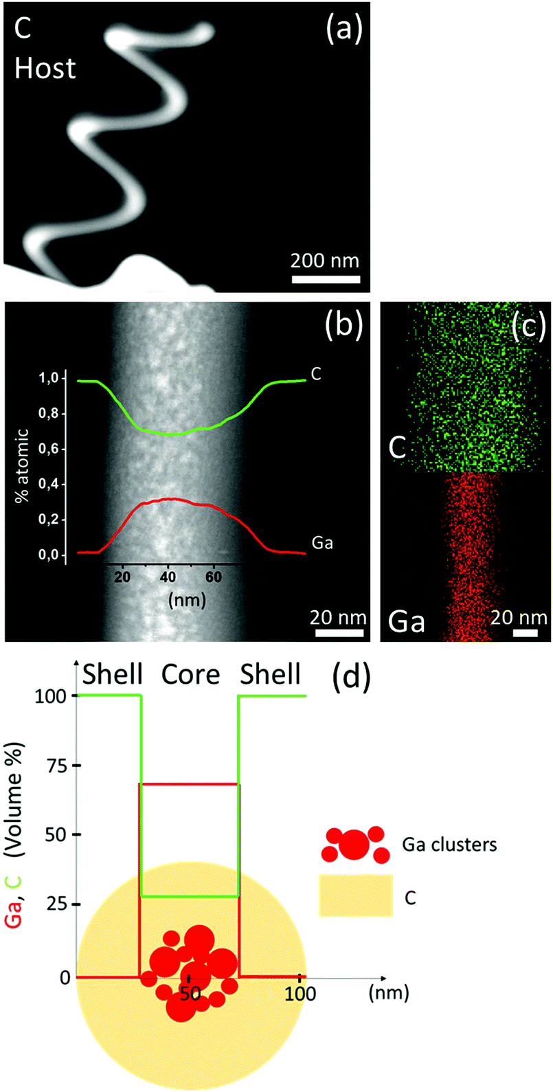 | ||
| Fig. 1 (a) STEM image of the C/Ga nanohelix fabricated with a phenanthrene (C14H10) gaseous precursor. (b) Thickness normalized EDX line scan profile across the nanohelix section reported in the same panel showing the average atomic percentage of elements as sensed by the e-beam crossing the helix wire. (c) EDX qualitative elemental maps of panel (b). (d) Schematic view of the wire cross section and related Ga and C volume composition profiles. | ||
Another scenario appears when a Ga ion beam is used to grow the silicon dioxide nanohelices (for growth details, see Methods section). As shown by the cross-section STEM-HAADF images and EDX qualitative maps, the nanowire still exhibits a core–shell architecture with respect to Ga content (Fig. 2a and b). The maximum Ga atomic percentage measured using the linear scan is approximately 50%, with the peak positioned at the nanostructure center and approaching a null value in the outer shell. The O-to-Si atomic ratio is about 2 (Fig. 2b), corresponding to stoichiometric SiO2, and it is constant throughout the whole structure. Thus, the outer shell is an alloy mainly composed by amorphous silicon dioxide (Fig. 2d).
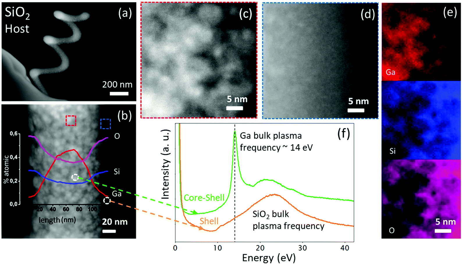 | ||
| Fig. 2 (a) STEM image of the SiO2/Ga nanohelix. (b) Thickness normalized EDX line scan profile across the nanohelix section showing the average atomic percentage of elements as sensed by the e-beam crossing the helix wire. Higher magnification HAADF-STEM image on the (c) core and (d) shell regions, as indicated by the red and blue dotted squares in panel (b). (e) EDX qualitative elemental maps of panel (c). (f) Electron energy loss spectroscopy (EELS) measurements performed along the nanowire cross section of the core–shell and only the shell. The Ga bulk plasma frequency is detected at around 14 eV and only in correspondence of the core region. | ||
A similar approach used for the carbon-based system was also applied to evaluate the volume concentration profile across the SiO2 based nanowire. Fig. S1 (ESI†) reveals a 68% Ga/28% SiO2/4% C core (110 nm thick) and an 8% Ga/88% SiO2/4% C shell (average thickness around 10 nm). The core is mostly featured by well evident metallic Ga-clusters with an average diameter of about 12 nm (Fig. 2c). Moreover, the Ga-core is thicker within the SiO2-nanohelix than within the C-nanohelix.
The incorporation of Ga ions depends on the scattering efficiency and diffusion length of scattered ions inside the host matrix, and this represents the limiting factor for the core dimensions. Similar composition profiles have been found for carbon nanopillar growth using focused ion beam induced deposition (FIBID).44 Moreover, our results are consistent with those of the previous studies regarding the interaction between a 30 kV focused Ga+-ion beam and silicon,45 silicon oxide46 and amorphous carbon as host materials.47
In the silicon-based material, Ga implantation starts at the surface because of the large interaction between Ga+ and Si nuclei,45 similar to our SiO2-based helical system where the Ga core is in close proximity to the wire surface (Fig. 2b). On the other hand, for amorphous carbon, McKenzie et al.47 observed that the Ga concentration peak shifted below the surface of the implant by tens of nanometers. Actually, such a shift was also observed in the growth of C-based free-space wires by using the FIBID technique.44 Similar results are also noticeable in our C-based nanohelices where the center position of the Ga core is at about 50 nm far from the wire surface, and slightly downshifted with respect to the processing beam. The rationale for this is the negligible solubility of carbon in Ga:48,49 actually, liquid Ga works as a photocatalyst for the growth of carbon multiwall nanotubes, where Ga is confined and localized in the nanostructure.49 Noteworthily, this intrinsic plasmonic Ga-core can photocatalyze the growth of the carbon nanohelices, thus representing another advantage of the proposed one-step direct synthesis.
Conversely, silicon is more soluble than C in liquid Ga.50 This, in combination with the poor tendency of Ga liquid clusters to retain oxygen, rather than silicon, favours the diffusion of metallic Ga-clusters in a SiO2-matrix, resulting in a larger Ga core, as compared to that in the C case.
Therefore, the difference in behaviour of Ga-clusters with silicon dioxide and carbon can be used to tailor different core-to-shell thickness ratios. In particular, a CSR value of approximately 11 was evaluated for SiO2, which is almost an order of magnitude larger than that achieved for carbon-based system (CSR = 1.3). It is worth noting that here we are reporting the fundamental effect of material interactions on the CSR of nanohelices fabricated under optimal conditions: the FIBID process was focused on the growth of carbon- and SiO2-based nanohelices by using the Ga+-ion dose allowing controlled evolution of the nanohelices in the third dimension to be obtained, with a vertical pitch (VP) (Fig. 4c) of about 500 nm. In the supporting section (Fig. S2, ESI†) we show the effect of ion dose deviation from the optimal value on the helix morphology; small dose variations can lead to a dramatic effect on 3D nanohelix growth. Therefore, because of such constrictions, we can argue that process parameters such as ion energy or beam current in the very narrow optimal ion dose window can lead to variations of the nanohelix CSR, but in a limited amount.
Fig. 2e, top panel, highlights Ga patches distributed all over the helix wire where oxygen was not detected, as reported in the bottom panel. Conversely, oxygen and silicon show the same spatial distribution (bottom and middle panel), suggesting the preferential bonding of O with Si rather than with Ga, and the consequent formation of SiO2. Thereby, it seems reasonable that Ga is present in the metallic phase. This is consistent with the study reported in ref. 46, where it is demonstrated that, for high Ga+ implantation doses in SiO2, the electronic configuration of the embedded Ga assumes a metallic valence, forming metallic agglomerates.
The metallic phase of Ga-clusters is highlighted by the detection of Ga plasma frequency obtained by electron energy loss. The spectra in Fig. 2f are collected in two distinct regions, as reported in the STEM-HAADF survey image (Fig. 2b): corresponding to the Ga-cluster inside the core and on the shell. From the core portion, a narrow peak originates at around 14 eV, corresponding to the plasma frequency of Ga in the metallic form.17,31
Furthermore, the high resolution STEM did not indicate any lattice fringes inside the Ga-clusters; therefore, we infer that the Ga-clusters are liquid and/or amorphous. This represents an advantage for their plasmonic behavior, since the polymorphism of Ga has been recently optically analyzed by Gutierrez et al.51,52 demonstrating that liquid and amorphous Ga have a perfect Drude response, allowing resonances to be tuned from UV to NIR. On the other hand, crystalline phases, predicted to be stable at room temperature, such as α-Ga and β-Ga, are indeed characterized by intraband absorption at photon energies below 2.2 eV contributing to plasmon resonance quenching in the VIS and NIR regions. Furthermore, both liquid and amorphous Ga, contrary to crystalline forms, have the advantage of being free from crystalline defects such as grain boundaries that quench and broaden plasmonic resonances and decrease the free electron lifetime.
With a large plasma frequency of about 14 eV, Ga isolated clusters are known to provide localized surface plasmon resonances in the UV spectral range. However, in our nanostructures, Ga-clusters are embedded in a dielectric matrix, with a large refractive index that could lower the oscillation frequency of conduction electrons in the metallic clusters, similar to metal-core/oxide-shell nanoparticles.53,54 We have used Mie theory55 to predict the effect of the matrix and of the dispersion on the Ga localized surface plasmon resonance. As shown in Fig. 3, a single Ga NP under vacuum, with the Ga-cluster size inferred using TEM analysis (12 nm average diameter, see Fig. 2b and c), shows a resonance at 200 nm (Fig. 3a), which red-shifts up to 280 nm when considering the NP embedded in a SiO2 matrix (Fig. 3b). Collective interactions between plasmonic dipoles, induced by the small or null interparticle distance within the helix nanowire, are expected to red-shift and broaden the plasmonic resonance. We performed finite-difference time-domain (FDTD) simulations considering a cylindrical element (diameter of 100 nm and height of 100 nm) of the helix nanowire with interacting Ga NPs embedded in a SiO2 matrix. The Ga NPs were assumed with a random distribution, therefore including the possibility of null interparticle distance and/or compenetration. As shown in Fig. 3c, the absorption collective resonance red-shifts up to 400 nm and undergoes a significant broadening from UV to NIR. Hence, the assembly of the achiral Ga-nanoclusters in a chiral fashion along the helical path is expected to result in circular dichroism and optical activity from UV to NIR.
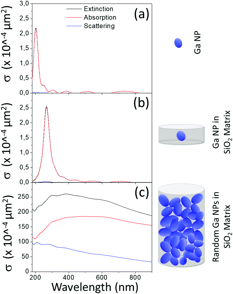 | ||
| Fig. 3 Calculated extinction, scattering and absorption cross sections for: (a) a single Ga NP (12 nm diameter) in vacuum, (b) a single Ga NP (12 nm diameter) in a SiO2 matrix cylinder (diameter of 100 nm and height of 15 nm), and (c) a random distribution of Ga NPs (12 nm diameter) in a SiO2 matrix cylinder (diameter of 100 nm and height of 100 nm). | ||
The two core–shell architectures were shaped into right-handed (RH) nanohelices periodically arranged into 20 μm × 20 μm square arrays (Fig. 4).
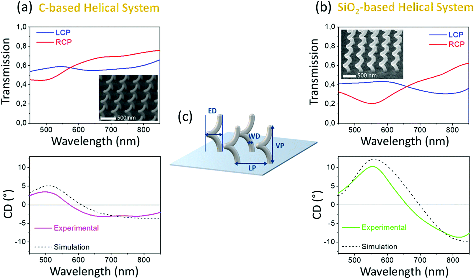 | ||
| Fig. 4 Transmission spectra under normal incidence of right (TRCP)- and left (TLCP)-handed circularly polarized light (top panels) and CD expressed in degree units (bottom panels) for (a) C- and (b) SiO2 helical systems. The simulated CD curves are superimposed with the experimental ones in the bottom panels. The insets report scanning electron microscope (SEM) images of array portions. (c) Illustrative scheme of the geometrical parameters of the helix arrays. The arrays consist of nanohelices with VP of 500 nm, 1 loop, lattice period (LP) of 500 nm, external diameter (ED) of 340 nm, and wire diameter (WD) of 130 nm for the SiO2 helices array, while ED of 280 nm, and WD of 100 for the C-one. | ||
Transmission spectra under normal incidence of right (TRCP)- and left (TLCP)-handed circularly polarized light through the samples were collected (Fig. 4a and b top panel) and the related circular dichroism (CD), expressed in terms of the ellipticity as:
 | (1) |
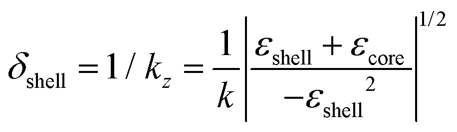
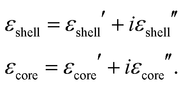
To understand the difference in the transmission behavior of the two systems, it is worth noting that the evanescent fields promoted by the core surface plasmon waves at the core–shell interface are strongly affected by the material dispersions and shell thickness. In particular, the near-field exponentially decays into the dielectric shell with distance |z| from the core–shell interface:54
| E = (Ex, 0, Ez)exp(−kzz)exp[i(kxx − ωt)], | (2) |
 | (3) |
 | (4) |
A simple calculation, by considering the optical dispersion values shown in Fig. S4 (ESI†) at 500 nm and 560 nm for C- and SiO2-based materials (optical constant calculation method reported in Fig. S3, ESI†), respectively (corresponding to the wavelength of maximum CD in the VIS for C- and SiO2-based nanohelices as reported in Fig. 4), led to δ values of 40 nm for C and up to 450 nm for SiO2, respectively. Therefore, in the C shell case, we expect the inhibition of plasmon propagation to the surface, since the decay length of the plasmon is comparable with the shell thickness. On the other hand, the extremely thin and low loss SiO2 shell can efficiently support plasmon propagation. The above mentioned calculations clearly indicate how the suppression of plasmonic phenomena makes the optical behavior of the carbon-based system comparable to that of a template triggered by photonic mechanism. Indeed, if the incident light wavelength matches the pitch of the dielectric helix,24,56 resonances at different wavelengths arise for both the incident circular polarizations. In particular, depending on the mutual handedness between the nanohelix and incident light, a stronger field confinement is obtained when both exhibit the same rotation sense.
On the other hand, the SiO2-based core–shell nanohelices exhibit a very sharp resonance at 560 nm; here the transmission level is lower than that of the C-based system, as a result of the enhanced core plasmonic absorption, and the CD is significantly boosted up to 11° (Fig. 4b bottom panel). A direct comparison can be made with platinum-based systems,36 realized by using the same Gallium ion beam in combination with a metalorganic precursor of Pt, and with exactly the same set of geometrical features. Because of the larger amount of metal embedded in the core of the helix through our optimized fabrication procedure, as well as the reduced system losses, the measured CD in the same spectral range is nearly doubled. As discussed in the introduction, another method for the manufacture of continuous and well separated metal nanohelices that operate in the VIS range is the shadow growth from ordered seed elements.25 In a wafer standing configuration, these chiral thin films have demonstrated their highest CD value of 6 degrees at 600 nm from nanohelices in Ag/Cu alloy, with VP = 55 nm, N = 2, ED = 32 nm, and LP = 53 nm.57 Other technologies based on chemical synthetic techniques and where the helices are dispersed in solution have instead reached VIS CD values of the order of hundreds of millidegrees.58,59
The measurements for both architectures were also compared with the simulated spectra (Fig. 4a and b bottom panel), obtained by considering each helix to be composed of two nanohelices: the helixcore, characterized by the optical dispersions as shown in Fig. S4a and b top panel (ESI†), and the helixshell featured by the optical dispersions as shown in Fig. S4a and b (ESI†) bottom panel. A good agreement is gathered between the measured and simulated spectra with the used electromagnetic model.
The origin of the large CD value in SiO2-based core–shell nanohelices was also investigated by comparing the optical response of FIBID nanohelices (Fig. 4b, top panel) with that obtained from nanohelix arrays fabricated using a focused electron beam induced deposition (FEBID) approach, completely free of gallium, with similar structural features of the FIBID ones in terms of wire diameter, vertical pitch and external diameter. Such helical shape nanostructures were realized by using a TEOS precursor and resulted as completely dielectric as reported in the TEM analysis of Fig. S5 (ESI†). In particular, the thickness normalized EDX line scan profile radially performed along the helix nanowire (Fig. S5a, top panel, ESI†) shows a constant signal level for Si, O and C (Fig. S5a, bottom panel, ESI†). It can be concluded that the radial distribution of these elements is constant along the nanohelix section. Moreover, the Si atomic percentage is found to be half of that of oxygen, suggesting an O-to-Si atomic ratio of about 2, likely corresponding to the SiO2 composition as already observed for the above mentioned FIBID approach. The high resolution STEM analysis (Fig. S5b, ESI†) did not remark any lattice fringes inside the helix wire emphasizing the amorphous structure of those nanostructures fabricated by means of the FEBID approach. In that dielectric frame, the nanohelix array provides a very poor CD (Fig. S5c, ESI†) with respect to the Ga-rich helix counterpart (Fig. 4b, bottom panel) confirming the fundamental role of gallium as the plasmonic element.
As already pointed out, in the SiO2-based nanostructures, the near-field extends beyond the small dielectric shell, allowing plasmon propagation to the surface and plasmonic mode-hybridization. The latter can be experimentally highlighted with the observation of resonance broadening induced by plasmon dipole–dipole interactions60,61 in the SiO2-based helix arrays with identical structural features and different pitch numbers N,36 varying from 0.25 to 1 (Fig. S6 and S7, ESI†).
For our geometry, a quarter pitch helical element did not exhibit circular dichroism (Fig. S7a, ESI†), whereas a metallic half pitch helical element shows a resonant chiral behavior, indicating the formation of a light-interacting plasmonic dipole moment and suggesting the half pitch helix as the fundamental unit element. Fig. S7a (ESI†) shows the bandwidth increase due to plasmonic mode hybridization obtained with two unit elements vertically stacked (N = 1),36 in a good agreement with the simulation of Fig. S7b (ESI†). Therefore, the continuity between the two above mentioned unit elements maximizes the coupling strength60,61 and boosts the CD to about 11°.
3. Conclusions
In summary, we report the realization of gallium chiral nanostructures using a direct one-step nanofabrication. The structures are grown using focused ion beam induced deposition, and the metal deposit originates from the Ga liquid ion source of the system. The combination of the ion beam with a properly selected host matrix enables the fabrication of Ga-core/dielectric-shell 3D nanostructures with tailorable optical behavior in the visible range. A thick shell of highly absorbing medium, such as amorphous carbon, strongly screens the plasmon propagation promoted by the Ga core, inducing a photonic behavior in the chiral nanostructures. Conversely, very efficient 3D Ga plasmonic architectures were obtained with low absorbing and tiny SiO2 dielectric shell, significantly thinner than the decay length of the evanescent field promoted by the surface plasmon waves at the core–shell interface. The reported results pave the way towards the development of nanostructures with increasing compositional and structural complexity and allow a new class of gallium-based core–shell 3D chiral nanostructures for polarized light handling to be envisioned.4. Methods
Sample fabrication
A copper TEM grid was used as the substrate for single helix growth in order to perform compositional and structural investigation. In particular, it was locked in a home-made sample holder and loaded in a dual configuration Focused Ion Beam (FIB)/SEM system, the Carl Zeiss Auriga40 Crossbeam, equipped with the Cobra FIB column and a gas injection system (GIS) with five channels.First, we partially milled the copper grid reducing its thickness in order to avoid the shadow effect during cross sectional TEM analysis. We have used a Ga+-ion beam with a beam current of 16 nA and an accelerating voltage of 30 keV.
After phenanthrene [C14H10] and tetraethyl orthosilicate (TEOS) [Si(OC2H5)4] precursors were locally injected into the samples, we optimized the injection distance between the copper grid and nozzle to obtain high growth control by a suitable gas density. The nanohelices were grown with a Ga+-ion beam current of 1 pA, an accelerating voltage of 30 keV, and a step size of 10 nm and dwell time of 400 ms for the C-based helical system and a step size of 1 nm and dwell time of 120 ms for the SiO2 one.
In order to both perform optical transmittance spectroscopy and prevent charge effects, arrays of carbon and SiO2-nanohelices were made on an indium tin oxide-on-glass substrate.
The chamber pressure ranged from 8 × 10⁻⁶ to 4 × 10⁻⁶ mbar during the deposition time of each row of arrays. To recover the pressure drop induced by effusion and the local depletion of the precursor density, we set a refresh time among consecutive rows of arrays. This stratagem allows high-dimensional uniformity to be obtained between nanohelices.62–64
TEM/EDX characterization
TEM and EDX analyses were performed on single nanohelices directly grown on a copper TEM grid using a Cs-probe-corrected TEM JEOL ARM200CF microscope operating in scanning mode at a primary beam energy of 200 keV and equipped with a 100 mm2 silicon drift detector for energy dispersive X-ray spectroscopy. In order to obtain Z contrast sensitiveness from the images, the microscope was configured in high-angle annular dark-field mode with a convergence angle of 33 mrad and a collection angle between 68 and 280 mrad (inner and outer collection angles of the dark-field detector). STEM-EDX spectroscopy was performed on a helix section. The signal was collected by scanning the same region multiple times with a dwell time of 1 ms. A GATAN GIF Quantum ER was used for electron energy loss spectroscopy measurements in the low-loss region.Optical characterization
In order to quantify the CD of chiral arrays, the transmission spectra were recorded using a confocal configuration by illuminating the sample with light (450–850 nm) from a tungsten lamp focalized by using a condenser with numerical aperture (NA) < 0.1 and collecting the transmitted light using a 40× objective lens with NA = 0.9. Circular polarization excitation was achieved using a combination of a linear polarizer and an achromatic quarter-wave plate. The microscope output image is collected and reconstructed on the entrance slits of a 200 mm spectrometer coupled to a charge-coupled device camera for measurements in the VIS/NIR spectral range. The light transmission was calculated with respect to light transmitted by the unpatterned substrate.Numerical simulations
To evaluate the spectral properties of the helix samples, we simulated their electromagnetic response at optical frequencies using commercial FDTD-based software (Lumerical FDTD Solutions) and the post-processing of data was completed by means of several Matlab codes. The substrate was not included in the simulations.Conflicts of interest
There are no conflicts to declare.Acknowledgements
This work was supported by Project “INNOSENSE” funded by MIUR – Italian Ministry of Research CUP: F87G18000010001, Progetto Tecnopolo per la Medicina di precisione, Deliberazione della Giunta Regionale no. 2117. The work was also partially supported by the regional project Innonetwork “IN-AIR” CUP: B37H17004840007 and regional project Innonetwork “M3O3” CUP: B37H17005320007. The authors are grateful to the “Tecnopolo per la medicina di precisione” (TecnoMed Puglia) – Regione Puglia: DGR no. 2117 del 21/11/2018 CUP: B84I18000540002 and “Tecnopolo di Nanotecnologia e Fotonica per la medicina di precisione” (TECNOMED) – FISR/MIUR-CNR: delibera CIPE no. 3449 del 7-08-2017 CUP: B83B17000010001. The author ML acknowledges the support of the European Union's Horizon 2020 research and innovation program under grant agreement no. 899598 – PHEMTRONICS.References
- S. Jahani and Z. Jacob, All-Dielectric Metamaterials, Nat. Nanotechnol., 2016, 11(1), 23–36, DOI:10.1038/nnano.2015.304.
- A. I. Kuznetsov, A. E. Miroshnichenko, M. L. Brongersma, Y. S. Kivshar and B. Luk’yanchuk, Optically Resonant Dielectric Nanostructures, Science, 2016, 354(6314), aag2472, DOI:10.1126/science.aag2472.
- X. Duan, S. Kamin and N. Liu, Dynamic Plasmonic Colour Display, Nat. Commun., 2017, 8, ncomms14606, DOI:10.1038/ncomms14606.
- D. Wang, A. Yang, W. Wang, Y. Hua, R. D. Schaller, G. C. Schatz and T. W. Odom, Band-Edge Engineering for Controlled Multi-Modal Nanolasing in Plasmonic Superlattices, Nat. Nanotechnol., 2017, 12(9), 889–894, DOI:10.1038/nnano.2017.126.
- M. Esposito, F. Todisco, S. Bakhti, A. Passaseo, I. Tarantini, M. Cuscunà, N. Destouches and V. Tasco, Symmetry Breaking in Oligomer Surface Plasmon Lattice Resonances, Nano Lett., 2019, 19(3), 1922–1930, DOI:10.1021/acs.nanolett.8b05062.
- D. Simeone, M. Esposito, M. Scuderi, G. Calafiore, G. Palermo, A. De Luca, F. Todisco, D. Sanvitto, G. Nicotra, S. Cabrini, V. Tasco, A. Passaseo and M. Cuscunà, Tailoring Electromagnetic Hot Spots toward Visible Frequencies in Ultra-Narrow Gap Al/Al2O3 Bowtie Nanoantennas, ACS Photonics, 2018, 5(8), 3399–3407, DOI:10.1021/acsphotonics.8b00665.
- F. D’apuzzo, M. Esposito, M. Cuscunà, A. Cannavale, S. Gambino, G. E. Lio, A. De Luca, G. Gigli and S. Lupi, Mid-Infrared Plasmonic Excitation in Indium Tin Oxide Microhole Arrays, ACS Photonics, 2018, 5(6), 2431–2436, DOI:10.1021/acsphotonics.8b00214.
- P. Adriana, E. Marco, C. Massimo and T. Vittorianna, Materials and 3D Designs of Helix Nanostructures for Chirality at Optical Frequencies, Adv. Opt. Mater., 2017, 5(16), 1601079, DOI:10.1002/adom.201601079.
- S. I. Lepeshov, A. E. Krasnok, P. A. Belov and A. E. Miroshnichenko, Hybrid Nanophotonics, Phys.-Usp., 2019, 61(11), 1035, DOI:10.3367/UFNe.2017.12.038275.
- G. V. Naik, V. M. Shalaev and A. Boltasseva, Alternative Plasmonic Materials: Beyond Gold and Silver, Adv. Mater., 2013, 25(24), 3264–3294, DOI:10.1002/adma.201205076.
- S. Kim, J.-M. Kim, J.-E. Park and J.-M. Nam, Nonnoble-Metal-Based Plasmonic Nanomaterials: Recent Advances and Future Perspectives, Adv. Mater., 2018, 30(42), 1704528, DOI:10.1002/adma.201704528.
- R. Reena, Y. Kalra and A. Kumar, Ellipsoidal All-Dielectric Fano Resonant Core-Shell Metamaterials, Superlattices Microstruct., 2018, 118, 205–212, DOI:10.1016/j.spmi.2018.03.067.
- M. Esposito, V. Tasco, F. Todisco, M. Cuscunà, A. Benedetti, D. Sanvitto and A. Passaseo, Triple-Helical Nanowires by Tomographic Rotatory Growth for Chiral Photonics, Nat. Commun., 2015, 6, 6484, DOI:10.1038/ncomms7484.
- Z. Shi, M. Khorasaninejad, Y.-W. Huang, C. Roques-Carmes, A. Y. Zhu, W. T. Chen, V. Sanjeev, Z.-W. Ding, M. Tamagnone, K. Chaudhary, R. C. Devlin, C.-W. Qiu and F. Capasso, Single-Layer Metasurface with Controllable Multiwavelength Functions, Nano Lett., 2018, 18(4), 2420–2427, DOI:10.1021/acs.nanolett.7b05458.
- Y. Gutiérrez, R. Alcaraz de la Osa, D. Ortiz, J. M. Saiz, F. González and F. Moreno, Plasmonics in the Ultraviolet with Aluminum, Gallium, Magnesium and Rhodium, Appl. Sci., 2018, 8(1), 64, DOI:10.3390/app8010064.
- Y. Yang, J. M. Callahan, T.-H. Kim, A. S. Brown and H. O. Everitt, Ultraviolet Nanoplasmonics: A Demonstration of Surface-Enhanced Raman Spectroscopy, Fluorescence, and Photodegradation Using Gallium Nanoparticles, Nano Lett., 2013, 13(6), 2837–2841, DOI:10.1021/nl401145j.
- M. W. Knight, T. Coenen, Y. Yang, B. J. M. Brenny, M. Losurdo, A. S. Brown, H. O. Everitt and A. Polman, Gallium Plasmonics: Deep Subwavelength Spectroscopic Imaging of Single and Interacting Gallium Nanoparticles, ACS Nano, 2015, 9(2), 2049–2060, DOI:10.1021/nn5072254.
- S. So, J. Mun and J. Rho, Simultaneous Inverse Design of Materials and Structures via Deep Learning: Demonstration of Dipole Resonance Engineering Using Core–Shell Nanoparticles, ACS Appl. Mater. Interfaces, 2019, 11(27), 24264–24268, DOI:10.1021/acsami.9b05857.
- A. Sheverdin and C. Valagiannopoulos, Core-Shell Nanospheres under Visible Light: Optimal Absorption, Scattering, and Cloaking, Phys. Rev. B: Condens. Matter Mater. Phys., 2019, 99(7), 075305, DOI:10.1103/PhysRevB.99.075305.
- P. Yu, Y. Yao, J. Wu, X. Niu, A. L. Rogach and Z. Wang, Effects of Plasmonic Metal Core -Dielectric Shell Nanoparticles on the Broadband Light Absorption Enhancement in Thin Film Solar Cells, Sci. Rep., 2017, 7(1), 1–10, DOI:10.1038/s41598-017-08077-9.
- W. Liu, J. Zhang, B. Lei, H. Ma, W. Xie and H. Hu, Ultra-Directional Forward Scattering by Individual Core-Shell Nanoparticles, Opt. Express, 2014, 22(13), 16178–16187, DOI:10.1364/OE.22.016178.
- W. Liu, A. E. Miroshnichenko, D. N. Neshev and Y. S. Kivshar, Broadband Unidirectional Scattering by Magneto-Electric Core–Shell Nanoparticles, ACS Nano, 2012, 6(6), 5489–5497, DOI:10.1021/nn301398a.
- R. Shi, D. L. Gao, H. Hu, Y. Q. Wang and L. Gao, Enhanced Broadband Spin Hall Effects by Core-Shell Nanoparticles, Opt. Express, 2019, 27(4), 4808–4817, DOI:10.1364/OE.27.004808.
- M. Thiel, M. Decker, M. Deubel, M. Wegener, S. Linden and G. von
![[thin space (1/6-em)]](https://www.rsc.org/images/entities/char_2009.gif) Freymann, Polarization Stop Bands in Chiral Polymeric Three-Dimensional Photonic Crystals, Adv. Mater., 2007, 19(2), 207–210, DOI:10.1002/adma.200601497.
Freymann, Polarization Stop Bands in Chiral Polymeric Three-Dimensional Photonic Crystals, Adv. Mater., 2007, 19(2), 207–210, DOI:10.1002/adma.200601497. - A. G. Mark, J. G. Gibbs, T.-C. Lee and P. Fischer, Hybrid Nanocolloids with Programmed Three-Dimensional Shape and Material Composition, Nat. Mater., 2013, 12(9), 802–807, DOI:10.1038/nmat3685.
- L. Hirt, A. Reiser, R. Spolenak and T. Zambelli, Additive Manufacturing of Metal Structures at the Micrometer Scale, Adv. Mater., 2017, 29(17), 1604211, DOI:10.1002/adma.201604211.
- M. Esposito, V. Tasco, F. Todisco, A. Benedetti, I. Tarantini, M. Cuscunà, L. Dominici, M. De Giorgi and A. Passaseo, Tailoring Chiro-Optical Effects by Helical Nanowire Arrangement, Nanoscale, 2015, 7(43), 18081–18088, 10.1039/C5NR04674B.
- V. Tasco, M. Esposito, F. Todisco, A. Benedetti, M. Cuscunà, D. Sanvitto and A. Passaseo, Three-Dimensional Nanohelices for Chiral Photonics, Appl. Phys. A: Mater. Sci. Process., 2016, 122(4), 280, DOI:10.1007/s00339-016-9856-6.
- M. Wang, R. Salut, H. Lu, M.-A. Suarez, N. Martin and T. Grosjean, Subwavelength Polarization Optics via Individual and Coupled Helical Traveling-Wave Nanoantennas, Light: Sci. Appl., 2019, 8(1), 1–8, DOI:10.1038/s41377-019-0186-2.
- D. Kosters, A. de Hoogh, H. Zeijlemaker, H. Acar, N. Rotenberg and L. Kuipers, Core-Shell Plasmonic Nanohelices, ACS Photonics, 2017, 4(7), 1858–1863, DOI:10.1021/acsphotonics.7b00496.
- M. Losurdo, A. Suvorova, S. Rubanov, K. Hingerl and A. S. Brown, Thermally Stable Coexistence of Liquid and Solid Phases in Gallium Nanoparticles, Nat. Mater., 2016, 15(9), 995–1002, DOI:10.1038/nmat4705.
- M. Yarema, M. Wörle, M. D. Rossell, R. Erni, R. Caputo, L. Protesescu, K. V. Kravchyk, D. N. Dirin, K. Lienau, F. von Rohr, A. Schilling, M. Nachtegaal and M. V. Kovalenko, Monodisperse Colloidal Gallium Nanoparticles: Synthesis, Low Temperature Crystallization, Surface Plasmon Resonance and Li-Ion Storage, J. Am. Chem. Soc., 2014, 136(35), 12422–12430, DOI:10.1021/ja506712d.
- I. Utke, P. Hoffmann and J. Melngailis, Gas-Assisted Focused Electron Beam and Ion Beam Processing and Fabrication, J. Vac. Sci. Technol., B, 2008, 26(4), 1197–1276, DOI:10.1116/1.2955728.
- R. Kometani and S. Ishihara, Nanoelectromechanical Device Fabrications by 3-D Nanotechnology Using Focused-Ion Beams, Sci. Technol. Adv. Mater., 2009, 10(3), 034501, DOI:10.1088/1468-6996/10/3/034501.
- J. Fujita, M. Ishida, T. Ichihashi, T. Sakamoto, Y. Ochiai, T. Kaito and S. Matsui, Structure and Resonant Characteristics of Amorphous Carbon Pillars Grown by Focused-Ion-Beam-Induced Chemical Vapor Deposition, Jpn. J. Appl. Phys., 2002, 41(6S), 4423, DOI:10.1143/JJAP.41.4423.
- M. Esposito, V. Tasco, F. Todisco, M. Cuscunà, A. Benedetti, M. Scuderi, G. Nicotra and A. Passaseo, Programmable Extreme Chirality in the Visible by Helix-Shaped Metamaterial Platform, Nano Lett., 2016, 16(9), 5823–5828, DOI:10.1021/acs.nanolett.6b02583.
- J. M. McMahon, G. C. Schatz and S. K. Gray, Plasmonics in the Ultraviolet with the Poor Metals Al, Ga, In, Sn, Tl, Pb, and Bi, Phys. Chem. Chem. Phys., 2013, 15(15), 5415–5423, 10.1039/C3CP43856B.
- S. Catalán-Gómez, A. Redondo-Cubero, F. J. Palomares, L. Vázquez, E. Nogales, F. Nucciarelli, B. Méndez, N. Gordillo and J. L. Pau, Size-Selective Breaking of the Core–Shell Structure of Gallium Nanoparticles, Nanotechnology, 2018, 29(35), 355707, DOI:10.1088/1361-6528/aacb91.
- A. Bhardwaj and S. S. Verma, Size Dependent Plasmonic Properties of Ga@Ag & Cs@Ag Liquid–Metal Nanospheres, Opt. Commun., 2019, 452, 264–272, DOI:10.1016/j.optcom.2019.07.049.
- M. de la Mata, S. Catalán-Gómez, F. Nucciarelli, J. L. Pau and S. I. Molina, High Spatial Resolution Mapping of Localized Surface Plasmon Resonances in Single Gallium Nanoparticles, Small, 2019, 15(43), 1902920, DOI:10.1002/smll.201902920.
- K.-H. Kim and Y.-S. No, Subwavelength Core/Shell Cylindrical Nanostructures for Novel Plasmonic and Metamaterial Devices, Nano Converg., 2017, 4(1), 32, DOI:10.1186/s40580-017-0128-8.
- S. Venkataramanababu, G. Nair, P. Deshpande, M. A. Jithin, S. Mohan and A. Ghosh, Chiro-Plasmonic Refractory Metamaterial with Titanium Nitride (TiN) Core–Shell Nanohelices, Nanotechnology, 2018, 29(25), 255203, DOI:10.1088/1361-6528/aabb4a.
- R. Kometani, T. Ichihashi, K. Kanda, T. Suzuki, K. Niihara, S. Ishihara, T. Kaito and S. Matsui, Resistivity Change of the Diamondlike Carbon, Deposited by Focused-Ion-Beam Chemical Vapor Deposition, Induced by the Annealing Treatment, J. Vac. Sci. Technol., B, 2008, 26(6), 2628–2631, DOI:10.1116/1.2978400.
- T. Morita, R. Kometani, K. Watanabe, K. Kanda, Y. Haruyama, T. Hoshino, K. Kondo, T. Kaito, T. Ichihashi, J. Fujita, M. Ishida, Y. Ochiai, T. Tajima and S. Matsui, Free-Space-Wiring Fabrication in Nano-Space by Focused-Ion-Beam Chemical Vapor Deposition, J. Vac. Sci. Technol., B, 2003, 21(6), 2737–2741, DOI:10.1116/1.1630329.
- H. Gnaser, A. Brodyanski and B. Reuscher, Focused Ion Beam Implantation of Ga in Si and Ge: Fluence-Dependent Retention and Surface Morphology, Surf. Interface Anal., 2008, 40(11), 1415–1422, DOI:10.1002/sia.2915.
- D. W. Niles, T. Spicer and R. W. Kee, Using Electron Spectroscopy to Verify the Model of Ga Implanted during Focused Ion Beam Circuit Editing, J. Vac. Sci. Technol., B, 2012, 30(6), 062203, DOI:10.1116/1.4759249.
- W. R. McKenzie, Md. Z. Quadir, M. H. Gass and P. R. Munroe, Focused Ion Beam Implantation of Diamond, Diam. Relat. Mater., 2011, 20(8), 1125–1128, DOI:10.1016/j.diamond.2011.06.022.
- J. Fujita, R. Ueki, Y. Miyazawa and T. Ichihashi, Graphitization at Interface between Amorphous Carbon and Liquid Gallium for Fabricating Large Area Graphene Sheets, J. Vac. Sci. Technol., B: Microelectron. Nanometer Struct.--Process., Meas., Phenom., 2009, 27(6), 3063–3066, DOI:10.1116/1.3253542.
- Z. W. Pan, S. Dai, D. B. Beach, N. D. Evans and D. H. Lowndes, Gallium-Mediated Growth of Multiwall Carbon Nanotubes, Appl. Phys. Lett., 2003, 82(12), 1947–1949, DOI:10.1063/1.1563727.
- P. H. Keck and J. Broder, The Solubility of Silicon and Germanium in Gallium and Indium, Phys. Rev., 1953, 90(4), 521–522, DOI:10.1103/PhysRev.90.521.
- Y. Gutiérrez, M. Losurdo, P. García-Fernández, M. S. Maza, F. de la González, A. S. Brown, H. O. Everitt, J. Junquera and F. Moreno, Gallium Polymorphs: Phase-Dependent Plasmonics, Adv. Opt. Mater., 2019, 7(13), 1900307, DOI:10.1002/adom.201900307.
- Y. Gutiérrez, Y. Gutiérrez, M. Losurdo, P. García-Fernández, M. S. Maza, F. de la; González, A. S. Brown, H. O. Everitt, H. O. Everitt, J. Junquera, F. Moreno and F. Moreno, Dielectric Function and Plasmonic Behavior of Ga(II) and Ga(III), Opt. Mater. Express, 2019, 9(10), 4050–4060, DOI:10.1364/OME.9.004050.
- C. Langhammer, M. Schwind, B. Kasemo and I. Zorić, Localized Surface Plasmon Resonances in Aluminum Nanodisks, Nano Lett., 2008, 8(5), 1461–1471, DOI:10.1021/nl080453i.
- S. A. Maier, Plasmonics: Fundamentals and Applications, Springer, US, 2007 Search PubMed.
- Absorption and Scattering of Light by Small Particles|Wiley https://www.wiley.com/en-us/Absorption+and+Scattering+of+Light+by+Small+Particles-p-9780471293408 accessed Jun 10, 2020.
- K. Robbie, D. J. Broer and M. J. Brett, Chiral Nematic Order in Liquid Crystals Imposed by an Engineered Inorganic Nanostructure, Nature, 1999, 399(6738), 764–766, DOI:10.1038/21612.
- J. G. Gibbs, A. G. Mark, S. Eslami and P. Fischer, Plasmonic Nanohelix Metamaterials with Tailorable Giant Circular Dichroism, Appl. Phys. Lett., 2013, 103(21), 213101, DOI:10.1063/1.4829740.
- X. Lan, T. Liu, Z. Wang, A. O. Govorov, H. Yan and Y. Liu, DNA-Guided Plasmonic Helix with Switchable Chirality, J. Am. Chem. Soc., 2018, 140(37), 11763–11770, DOI:10.1021/jacs.8b06526.
- A. Kuzyk, R. Schreiber, Z. Fan, G. Pardatscher, E.-M. Roller, A. Högele, F. C. Simmel, A. O. Govorov and T. Liedl, DNA-Based Self-Assembly of Chiral Plasmonic Nanostructures with Tailored Optical Response, Nature, 2012, 483(7389), 311–314, DOI:10.1038/nature10889.
- E. Prodan, C. Radloff, N. J. Halas and P. Nordlander, A Hybridization Model for the Plasmon Response of Complex Nanostructures, Science, 2003, 302(5644), 419–422, DOI:10.1126/science.1089171.
- Y. R. Li, R. M. Ho and Y. C. Hung, Plasmon Hybridization and Dipolar Interaction on the Resonances of Helix Metamaterials, IEEE Photonics J., 2013, 5(2), 2700510, DOI:10.1109/JPHOT.2013.2259583.
- M. Esposito, V. Tasco, M. Cuscunà, F. Todisco, A. Benedetti, I. Tarantini, M. D. Giorgi, D. Sanvitto and A. Passaseo, Nanoscale 3D Chiral Plasmonic Helices with Circular Dichroism at Visible Frequencies, ACS Photonics, 2015, 2(1), 105–114, DOI:10.1021/ph500318p.
- M. Esposito, V. Tasco, F. Todisco, A. Benedetti, D. Sanvitto and A. Passaseo, Three Dimensional Chiral Metamaterial Nanospirals in the Visible Range by Vertically Compensated Focused Ion Beam Induced-Deposition. Adv, Opt. Mater., 2014, 2(2), 154–161, DOI:10.1002/adom.201300323.
- A. Benedetti, B. Alam, M. Esposito, V. Tasco, G. Leahu, A. Belardini, R. L. Voti, A. Passaseo and C. Sibilia, Precise Detection of Circular Dichroism in a Cluster of Nano-Helices by Photoacoustic Measurements, Sci. Rep., 2017, 7(1), 5257, DOI:10.1038/s41598-017-05193-4.
Footnote |
| † Electronic supplementary information (ESI) available. See DOI: 10.1039/d0mh01078b |
| This journal is © The Royal Society of Chemistry 2021 |