
 Open Access Article
 This Open Access Article is licensed under a
 Creative Commons Attribution 3.0 Unported Licence
Synthesis and electron-transport properties of N-trifluoromethylphenyl-phthalimides containing selenophene substituents†
Jun-ichi
Nishida‡
 *a,
Yoshiki
Morikawa‡
a,
Akito
Hashimoto‡
a,
Yasuyuki
Kita‡
a,
Hiroshi
Nishimoto‡
a,
Tomofumi
Kadoya‡
b,
Hiroyasu
Sato‡
c and
Takeshi
Kawase‡
a
*a,
Yoshiki
Morikawa‡
a,
Akito
Hashimoto‡
a,
Yasuyuki
Kita‡
a,
Hiroshi
Nishimoto‡
a,
Tomofumi
Kadoya‡
b,
Hiroyasu
Sato‡
c and
Takeshi
Kawase‡
a
aDepartment of Applied Chemistry, Graduate School of Engineering, University of Hyogo, Himeji, Hyogo 671-2280, Japan. E-mail: jnishida@eng.u-hyogo.ac.jp
bDepartment of Material Science, Graduate School of Science, University of Hyogo, Kouto, Kamigori-cho, Ako-gun, Hyogo 678-1297, Japan
cRigaku Corporation, Matsubaracho, Akishima, Tokyo 196-8666, Japan
First published on 29th October 2021
Abstract
Trifluoromethylphenyl substituted phthalimides (PIs) containing oligoselenophene and phenylselenophene substituents were synthesized. Spectroscopic studies show that increasing the number of selenophene units causes the UV-Vis and photoluminescence maxima of the selenophene substituted PIs to shift to longer wavelengths. Analysis of the single crystal structure shows that the biselenophene substituted derivative has a layered structure, no center of symmetry and a molecular network with close contacts between Se atoms. XRD patterns of the PI derivatives indicate they have similar layered structures. These substances were used to fabricate field-effect transistors (FET)s by using the vapor deposition method. The FET derived using the biselenophene substituted PI exhibits clear n-type characteristics with an electron mobility of ca. 10−4 cm2 V−1 s−1. The FET prepared using the more highly conjugated terselenophene derivative also displays n-type FET characteristics with a slightly higher threshold voltage. Moreover, n-type behavior is also displayed by a highly crystalline thin film generated from the phenylselenophene derivative. The LED light responsiveness of FET characteristics was investigated. While the FET formed from the terselenophene derivative maintains a saturation drain–source current (IDS) operation along with a three-fold increase of electron mobility upon irradiation, those derived from the biselenophene and phenylselenophene derivatives display Ohm's law-like IDS. The difference in light responses are discussed in terms of conductivity differences.
Introduction
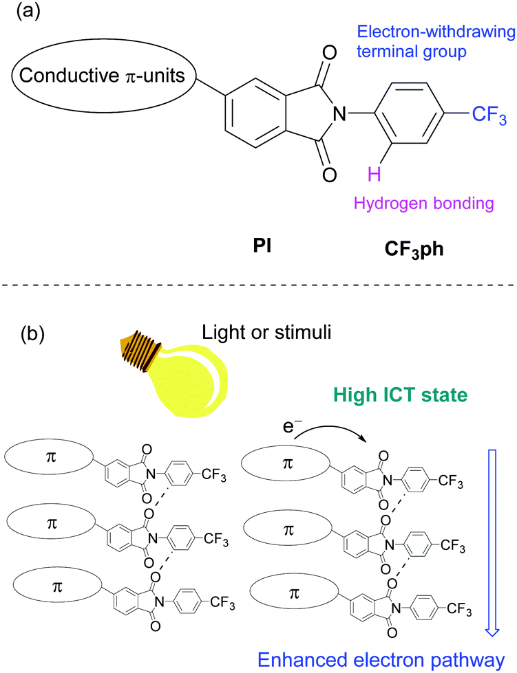
Organic n-type semiconductors have attracted great attention because they can be used in various electronic devices such as field-effect transistors (FETs)1–9 and organic photo-voltaic cells.10–12 As a result, studies of organic compounds that possess high electron mobilities have received great interest. In addition to these efforts, studies aimed at developing new types of substances with n-type semiconductor features have also focused on creating functional devices and understanding relationships that exist between molecular structures and electron-transport. In the context of FETs, it is known that imide derivatives containing extensive π-conjugated networks exhibit excellent electron mobilities.13–17 Attempts have also been made to create substances that have n-type semiconductor properties using small imide derivatives such as pyromellitic diimides.18 These efforts have demonstrated that, in general, good electron transportability exists in substances that possess two phthalimide (PI) moieties and an appropriate conjugated system such as those in anthracenes, pentalenes and pyrenes.19–21The PI moiety is an important electron-acceptor and, as a result, it has been incorporated into electron-acceptor units in electronics.22–24 An example exists in which microwire crystals of PI derivatives containing a dicyanocorannulene has been used in n-type FETs.24 However, simple asymmetric PI derivatives linked to several aromatic oligomers have not been usable as n-type semiconductors in FETs.
We anticipated that the electron transport properties of PIs could be enhanced by introducing electron movement pathways, such as networks containing carbonyl units25 and a 4-trifluoromethylphenyl (CF3ph) terminal group, and that these systems would be suitable for n-type semiconductors26 (Fig. 1a). In addition to searching for substances of this type, efforts in this area are motivated by the possibility of introducing responsiveness to external stimuli (Fig. 1b). For example, new compounds whose electron mobilities are depending on intramolecular charge transfer (ICT) states by light irradiation may be important components of multi-functional electronic devices27 and organic photodetectors.28,29
 | ||
| Fig. 1 (a) Molecular design of asymmetric PI compound and (b) the expected electron transporting pathway enhanced by external stimuli. | ||
In a previous report, we described studies that show that crystals of N-CF3ph-substituted PIs have well-aligned layered structures with no center of symmetry.30–32 The hydrogen bonding network between PI moieties and CF3ph groups serves as a template for making these crystals triboluminescent (TL)30,31 and for increasing excited state lifetimes.32 A potentially important characteristic of these PI derivatives is that linked conjugated components can be introduced.
The aim of the current investigation was to investigate the physical properties of PI derivatives that contain conductive π-moieties. For this purpose, we prepared the oligoselenophene linked PIs 1–3 and phenylselenophene analogue 4 (Fig. 2). We believed that these substances would have the following advantageous electronic features. Firstly, the large selenium (Se) atom in 1–4 is expected to enhance intermolecular interactions and orbital overlap. In fact, compounds containing selenophene moieties have been shown to have high charge mobilities.33–36 Secondly, because selenophenes have good electron-donating properties, PI derivatives containing these moieties should possess donor–acceptor (D-A) type structures and display ICT properties.37–41 Finally, crystals of the N-CF3ph-substituted PIs should have electron-withdrawing layered structures, which enhance the expression of n-type semiconductor characteristics needed for functioning FETs.
 | ||
| Fig. 2 Molecular structures of PIs 1–4 with selenophene units. Previously reported thiophene derivatives 2T and 3T.31 | ||
In the study described below, we synthesized PI derivatives 1–4, and carried out an X-ray crystal structure analysis, and spectroscopic and FET characteristics. In the effort, we observed that vapor deposited films of 2–4 function as n-type semiconductors in FETs. In addition, the drain–source currents (IDS) of these FETs irradiated using a light emitting diode (LED) can be controllably enhanced by varying the current flowing through the LED. The results are discussed and compared with those arising from the previously report about thiophene derivatives 2T and 3T.31
Results and discussion
PIs 2–4 were prepared using the mono-selenophene substituted derivative 1 as the starting material. Synthesis of 1 was accomplished by using Stille coupling reaction of bromo-PI 5 with 2-(tributylstannyl)selenophene (Scheme 1). Bromination of 1 with N-bromosuccinimide (NBS) gave bromo-selenophene 6 in 93% yield. Stille coupling reactions of 6 with the corresponding tin reagents then generated the biselenophene, terselenophene and phenylselenophene derivatives 2–4 in 60, 45, and 63% respective yields, which were purified by using recrystallisation from DMF or sublimation.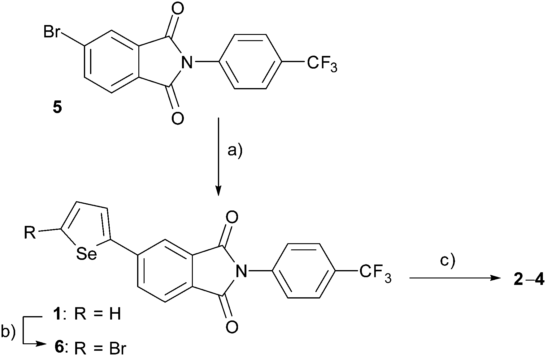 | ||
| Scheme 1 Preparation of target PIs 1–4 and bromine substituted precursor 6. Reagents: (a) Pd(PPh3)4, 2-(tributylstannyl)selenophene (y. 80%), (b) NBS (93%), (c) Pd(PPh3)4, 2-(tributylstannyl)selenophene for 2 (60%); 5-tributylstannyl-2,2′-biselenophene for 3 (45%); tributylstannylbenzene for 4 (63%). | ||
X-Ray crystal structural analysis was performed (Fig. 3 and Fig. S1A in ESI†)§ on a single crystal of the biselenophene 2, obtained by recrystallisation from DMF. In the crystal (space group is Pn), 2 exists in a well-aligned layered structure with no center of symmetry. Typical hydrogen bonding networks with distances of 2.783 and 2.804 Å exist in the PI and CF3ph layer between oxygen atoms of carbonyl groups and benzene ring hydrogens (Fig. 3b). Interactions also exist between the carbonyl groups. Moreover, the selenium atoms in the terminal selenophene rings are in close contact with distances of 3.836 and 3.849 Å that are near the sum of the van der Waals radius plus 0.1 Å. The crystal is isomorphic to that of previously reported bithiophene substituted PI 2T. However, the fact that the distances between the sulfur (S) atoms of the terminal thiophene rings in 2T (3.860 and 3.863 Å) are almost the same as those between the Se atoms in 2 suggests that intermolecular interaction between the Se atoms in 2 is larger than that between the S atoms in 2T.
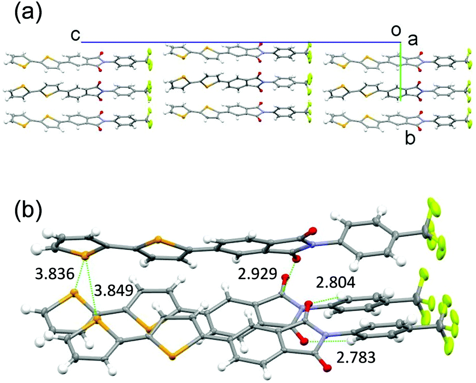 | ||
| Fig. 3 Crystal packing structures of biselenophene derivative 2. (a) Viewed along a-axis. (b) Close interactions. | ||
The respective PIs 1–4 are colourless, orange, dark red and yellow in solution and the solid states. Inspection of the absorption spectra of 1–4 in dichloromethane (DCM) (Fig. 4a and Fig. S3, ESI†) shows that the mono-selenophene derivative 1 has a maximum at 360 nm, and that 2 and 3 containing more extensively conjugated biselenophenes have respective maxima at 411 and 436 nm. The absorption maximum of biselenophene 2 occurs at a longer wavelength than that of the bithiophene 2T (399 nm). Moreover, elongation of the conjugated system by incorporation of phenyl group in 4 leads to a small increase in the wavelength maximum. Analysis of the photoluminescence (PL) spectra of these substances in DCM shows that the emission maximum is shifted to longer wavelengths when the number of selenophene rings increases (Fig. 4b). The same trends are observed for maxima in PL spectra of solid states of these substances (Fig. 4d). Solid diffuse reflection spectra of these PIs are given in Fig. 4c and Fig. S5 (ESI†). The peak-onset of 1 takes place at ca. 520 nm. As the number of selenophene rings increases, the peak-onset shifts to longer wavelengths (650 nm for 2 and 660 nm for 3). The spectroscopic data for these PI derivatives is given in Table 1.
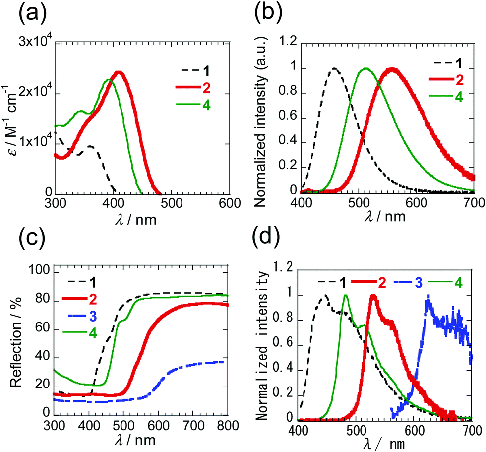 | ||
| Fig. 4 (a) UV-Vis (<10−5 M) and (b) PL spectra of 1, 2 and 4 in DCM. The spectra of 3 with low solubility are shown in Fig. S3 and S4 (ESI†). (c) Solid diffuse reflection spectra of 1–4. (d) PL spectra of 1–4 in solid states. | ||
| Compd |
λ
abs
(nm) (log![[thin space (1/6-em)]](https://www.rsc.org/images/entities/char_2009.gif) ε) ε) |
λ em (nm) (Φ) | λ end-abs_solid (nm) | λ em_solid (nm) (Φ) | E red |
|---|---|---|---|---|---|
| a In CH2Cl2. b Estimated by using 9,10-diphenylanthracene (λex = 366 nm, Φ = 0.86 in cyclohexane) as a standard.42 c Estimated from tangent intersections in solid diffuse reflection spectra. d Integrating sphere (λex = 366 nm). e V vs. Fc/Fc+, 0.1 M n-Bu4NPF6 in DMF, Pt electrode. Scan rate 100 mV s−1. f Low solubility. g Too low to decide. | |||||
| 1 | 360 (3.98) | 458 (0.16) | 520 | 448 (—)g | −1.68 |
| 2 | 411 (4.39) | 555 (0.04) | 650 | 531 (0.05) | −1.64 |
| 3 | 436 (—)f | 587 (—)g | 660 | 625 (—)g | —f |
| 4 | 392 (4.36) | 515 (0.13) | 540 | 483 (0.10) | –1.63 |
In addition, to evaluate the properties of PIs 2 and 3 in the thin films, absorption spectra were measured on thin films (60 nm) vacuum-deposited on quartz glasses (Fig. S6, ESI†). The longest absorption peaks occur at the shorter wavelengths (400 nm for 2 and 376 nm for 3) than those in DCM. Shifts to longer wavelengths are observed at the absorption ends, which are the result of aggregation.
To gain an understanding of the electronic transitions of the selenophene substituted PIs, calculations were performed at the RB3LYP/6-31G(d,p) level.43 The HOMOs and LUMOs of PIs 1–4 are shown in Fig. 5 and Fig. S17 (ESI†). The HOMO energy of mono-selenophene derivative 1 is 6.34 eV. As the conjugated system is extended to form biselenophene 2 and terselenophene 3, the energy of the HOMO increases and that of the LUMO decreases, leading to a smaller HOMO–LUMO energy gap. TD-DFT calculations were performed to assess the ICT nature of the electronic transitions. The results show that the oscillator strength is significantly enhanced as the number of selenophene rings in the PI derivatives increases. The data are summarized in Table 2 and calculated dipole moments are shown in Fig. 5.
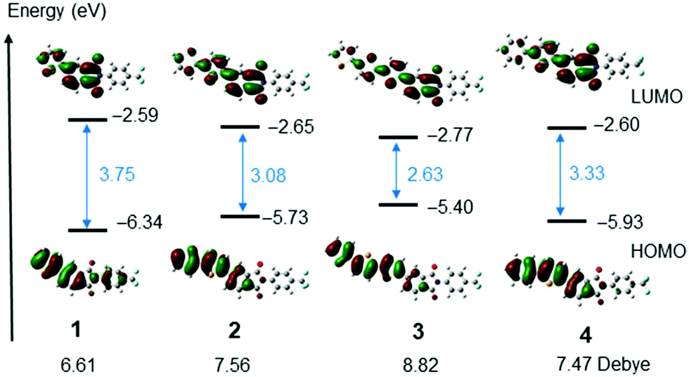 | ||
| Fig. 5 HOMOs and LUMOs of PIs 1–4 calculated using Gaussian 09 at RB3LYP/6-31G(d,p) level of theory. Dipole moments were also added. | ||
| Absorption/nm (Oscillator strength: f) | Assignments (ratios of contribution) | |
|---|---|---|
| a Calculated at the RB3LYP/6-31G(d,p) level of theory. | ||
| 1 | 381 (0.152) | HOMO to LUMO (66%) |
| 2 | 446 (0.564) | HOMO to LUMO (70%) |
| 3 | 517 (0.998) | HOMO to LUMO (70%) |
| 4 | 418 (0.470) | HOMO to LUMO (69%) |
The redox potentials of the selenophene substituted PIs were determined by using cyclic voltammetry (CV). PIs 1, 2 and 4 in DMF show cleanly reversible reduction waves (Ered of 1: –1.68, 2: –1.64, 4: –1.63 V vs. ferrocene (Fc)/Fc+) (Fig. S8, ESI†). Based on 4.8 eV of the HOMO of ferrocene, the LUMO energy of 2 is 3.2 eV.44 Compounds having the LUMO energy exhibit n-type semiconductor properties for FET, but tend to have high threshold voltages (Vth).26 On the other hand, in thin film states, electron injection seems to be improved. CV measurements on thin films of 2 and 3 deposited on ITO electrodes immersed in acetonitrile showed that reduction waves rise from around −1.1 V (ca. 3.6 eV) (Fig. S9, ESI†).
Bottom-contact type FETs were fabricated by using a vacuum deposition method with substrates equipped with interdigitated Au electrodes.45 A small white light emitting diode46 was installed on a shutter used for vapor deposition so that the distance from the substrate is controlled to be 1 cm (Fig. S10, ESI†). Surface treatment reagents such as hexamethyldisilazane were not used to avoid the possible occurrence of electron transfer between these reagents and PI derivatives during photoirradiation.
Measurements of the FETs were carried out at room temperature and under high vacuum conditions (10−5 Pa). PI derivatives 2–4 exhibit clear n-type characteristics. First, the FET containing biselenophene derivative 2 in the dark exhibits characteristic output curves with normal saturation current with the electron mobility of 1.3 × 10⁻⁴ cm2 V−1 s−1 (Fig. 6a).47 The electron mobility is enhanced to 8.9 × 10⁻⁴ cm2 V−1 s−1 by raising the substrate temperature to 100 °C during vapor deposition (Fig. S14, ESI†). The film containing the π-extended terselenophene derivative 3 also exhibits n-type FET behavior with a slightly high electron-mobility (4.2 × 10⁻⁴ cm2 V−1 s−1) and Vth (+29 V). The difference of Vth is consistent with the increased electron donating property of the π-extended selenophene group in 3. The FET containing phenylselenophene substituted PI 4 has a higher electron mobility compared with that of biselenophene 2 made at room temperature substrate. The data are summarized in Table 3.
 | ||
| Fig. 6 FET characteristics of (a) biselenophene derivative 2, (b) terselenophene derivative 3, and (c) phenylselenophene derivative 4 under dark conditions. FET characteristics of (d) 2, (e) 3, and (f) 4 during photoirradiation (bold red lines). Solid black lines are output curves under dark conditions. | ||
| Compd and condition | Mobilities (cm2 V−1 s−1) | Threshold voltage (V) | Conductivity at VG = 0 V (S m−1) |
|---|---|---|---|
| a Calculated from slopes of root IDS (IDS1/2) vs. VG. b Calculated from slope of IDSvs. VDS (between 0 and 100 V). c I LED = 12.9 mA. FETs of other compounds were performed in almost similar photoirradiation conditions. d Film deposited at substrate temp. 100 °C. e Large negative values. | |||
| 2 (in dark) | 1.3 × 10⁻⁴ | 5 | 4.6 × 10⁻⁶ |
| 2 (in LED)c | 7.7 × 10⁻⁵ | ≪0e | 1.4 × 10⁻³ |
| 2 (in dark)d | 8.9 × 10⁻⁴ | <0 | 1.1 × 10⁻⁴ |
| 2 (in LED)d | 6.6 × 10⁻⁴ | ≪0e | 9.7 × 10⁻³ |
| 3 (in dark) | 4.2 × 10⁻⁴ | 29 | 2.0 × 10⁻⁷ |
| 3 (in LED) | 1.2 × 10⁻³ | 21 | 3.8 × 10⁻⁵ |
| 4 (in dark) | 5.9 × 10⁻⁴ | <0 | 1.7 × 10⁻⁴ |
| 4 (in LED) | 1.0 × 10⁻⁴ | ≪0e | 7.6 × 10⁻³ |
| 3T (in dark) | 2.9 × 10⁻⁵ | 35 | 7.7 × 10⁻⁸ |
| 3T (in LED) | 1.2 × 10⁻⁴ | 23 | 3.1 × 10⁻⁶ |
Next, the effect of light irradiation on the characteristics of FETs prepared using these selenophene containing PI derivatives was assessed. An LED was employed for this purpose and the current flowing through the LED is given as ILED.46 A large amplification of the drain–source current (IDS) with respect to drain–source voltage (VDS) is observed. In the case of the FET prepared using 2, the maximum IDS increases approximately six times when ILED is 12.9 mA (Fig. 6d). No saturation IDS is observed, and the values increase in a manner that follows Ohm's law. The electron mobility, calculated by using a plot of IDS1/2 (at VDS 100 V) vs. VG,47 is estimated to be small because the VG dependence is small (Table 3). The increase of IDS promoted by irradiation is related to an increase in conductivity.48 An about three hundred times increase (Table 3) in conductivity, calculated as the difference when the gate voltage is not applied, is brought about by irradiation of FET 2.
On the other hand, in the output of the FET device containing 3 maintains saturation IDS during photoirradiation. The results of similar calculations47 show that the system has an approximately three times higher mobility and a lower Vth of +21 V (Table 3). The IDS response of the FET device made using 4 to photoirradiation is similar to that of 2, and the relationship between IDS and VDS is in accord with Ohm's law. The differences between the terselenophene derivative 3 and analogues 2 and 4 is likely the result of the differing lengths of their conjugated systems linked to the PI core.
In this system, ICT in conjugated systems containing PI core caused by light irradiation work to reduce Vth of electron transport. A long conjugated system gives a large Vth, but it stabilizes the characteristics of FET. Moreover, it might be possible to stabilize the FET characteristics even under photoirradiation by increasing the length of the systems. The increase in the rate of change in the maximum IDS is about 4 times large but the low off-current is maintained.
FETs generated using the related thiophene derivatives 2T and 3T were also subjected to measurements under the same conditions. A thin film containing the bithiophene 2T does not display FET characteristics, while that made from 3T displays n-type character (Fig. S12A, ESI†). While the electron mobility of the FET from 3T is almost an order of magnitude lower than that of the FET containing terselenophene 3, its responsiveness to light is close to that of 3. The results of these experiments suggest that photoirradiation of the FETs produces carriers required for electron transport on the thin film surface, and that the degree of change promoted by light depends on the molecular structure of the substituent on the PI backbone.
The relationship between the intensity of light of LED and amplification of the IDS for the FET devices was explored. The light intensity was adjusted by varying the ILED of the LED source (0.01, 0.28, 1.00, 1.75, 4.86, 7.72, 12.9 mA) (Fig. S11B). In the case of the FET composed of 2, IDS–VDS curves at VG = 0 V were extracted from measurements under each photoirradiation condition (Fig. S15, ESI†). Inspection of the results (Fig. 7a) shows that the IDS values and slopes of the IDS–VDS plot increase as ILED values increase. Furthermore, the plot given in Fig. 7b shows that maximum values of IDS (at VG = 0, and VDS = 100 V), which depend on the ILED values, change significantly at the initial stage when ILED is small and reach a maximum value as the light intensity increases. Overall, the observations shows that the substances in the thin films are sensitive to light and that the IDS values can be controlled by varying the intensity of light. In this way, the LED can act as another gate for transistors of this type. In Fig. 7c is shown a graph of the continuous changes occurring IDS as the LED is repeatedly switched on and off. Results of experiments when the VG of 100 V is applied are given in Fig. 7d–f. Synergistic use of VG and light is also possible.
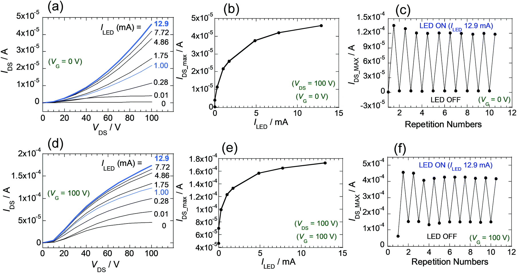 | ||
| Fig. 7 (a) IDS plots for FET 2 depending on ILED (at VG = 0 V). (b) IDS maxima of FET 2 with respect to ILED, (at VG = 0 V, and VDS = 100 V). (c) Changes in IDS values of FET 2 at VG = 0 V, when LED is switched on and off, repeatedly. (d–f) Similar experimental plots performed at VG 100 V. | ||
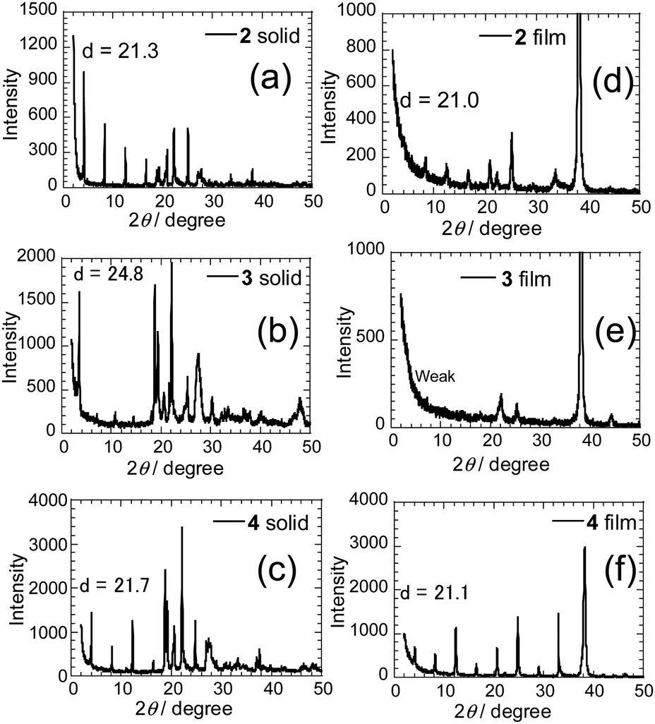
To determine the relationship that exists between molecular structures of the PI derivatives and FET characteristics, X-ray diffraction (XRD) patterns (a reflection mode) were obtained on the solid powders of 2–4 (Fig. 8a–c). Sharp reflection peaks are observed with the first reflection peaks corresponding to d-spacings of 21.3, 24.8 and 21.7 Å, which correspond to molecular lengths. The d-spacing value was also obtained for the mono-selenophene substituted 1 (Fig. S7A, ESI†). The results suggest that layered structures matching the molecular lengths are formed in the solid states. Next, XRD patterns of deposited films were obtained (Fig. 8d–f). High-order diffraction peaks are observed in the films of 2 and 4, with corresponding d-values from the first reflection peaks of 21.0 and 21.1 Å, which approximately match those in the solid states of these substances.
 | ||
| Fig. 8 XRD patterns of powders of (a) 2, (b) 3 and (c) 4, and thin films of (d) 2, (e) 3 and (f) 4. | ||
A weak layered structure seems to exist in the thin film of 3. The result suggests that the presence of a long π-conjugated substituent on the PI unit may lead to disadvantageous formation of a regular vapor deposition film. Moreover, high-order diffraction peaks were not observed in XRD patterns of films of thiophene-substituted PIs 2T and 3T. Thus, intermolecular interactions might be weaker in the thiophene derivatives than they are in the corresponding selenophene derivatives. On the other hand, the terminal phenylselenophene substituted analogue 4 shows strong diffraction peaks in both the solid state and thin film (Fig. 8c and f). Although the origin is unclear, thin films with high diffraction intensities tend to give larger current values and lower Vth.
In order to estimate the degree of the intermolecular interaction present in 2, the overlap integral was calculated using crystal structure data and the Energy Band Calculation program49 and compared with that reported for the bithiophene derivative 2T. The results show that a rather large degree of overlap up to 2.5 × 10⁻³ exists in the LUMO of 2 (Fig. 9) with relatively large values in the directions of t5 and t6. The overlap is similar to that in the LUMO of bithiophene 2T (Fig. S18, ESI†). On the other hand, a clear difference exists in the degree of overlap of the HOMOs. In the selenophene derivative 2, a maximum HOMO overlap value of 4.8 × 10⁻³ exists in the t2 direction, while it is 6.3 × 10⁻⁴ in the thiophene derivative 2T. The difference, which is likely a consequence of the larger atomic size of Se, is one reason for the different behaviors of vapor-deposited films of 2 and 2T.
 | ||
| Fig. 9 HOMO and LUMO overlap integrals of 2 estimated by using the energy band calculation program. | ||
Conclusions
In the study described above, we synthesized CF3ph-substituted asymmetric PI derivatives containing oligoselenophene and phenylselenophene substituents, and examined their optical and semiconductor properties. We found that derivatives containing the biselenophene or more highly conjugated unit, function as n-type semiconductors in FETs. Moreover, films on which these substances are deposited display a significant increase in IDS values and large shifts in Vth in response to visible light. This finding suggests that the controllable effect of light on the transistor properties of these FETs might be useful as a gate or when combined with a gate voltage.The results arising from these efforts do not enable us to discuss relationships that might exist between solid state photoresponsiveness and the presence or absence of a center of symmetry in the crystalline molecular arrangements. In any event, the selenophene substituted PIs probed in the study are expected to serve as model compounds to more carefully investigate the issue.
Conflicts of interest
There are no conflicts to declare.Acknowledgements
This study was financially supported by a Grant-in-Aid for Scientific Research on Innovation Areas “Stimuli-responsive Chemical Species for the Creation of Functional Molecules” (No. 2408) (JSPS KAKENHI Grant Number JP15H00959), and Scientific Research C (No. JP16K05896), (JP20K05651), (JP18K05091), (JP21K05024) and (JP20K15356). We thanks to the Division of Instrumental Analysis, Okayama University Advanced Science Research Center, for elemental analyses. We also thanks to Mr Tomoko Amimoto, the Natural Science Center for Basic Research and Development (N-BARD), Hiroshima University, for the HR-EI-MS measurements.Notes and references
- C. R. Newman, C. D. Frisbie, D. A. da Silva Filho, J. L. Bredas, P. C. Ewbank and K. R. Mann, Chem. Mater., 2004, 16, 4436–4451 CrossRef CAS.
- A. R. Murphy and J. M. J. Frechet, Chem. Rev., 2007, 108, 1066–1096 CrossRef PubMed.
- Y. Sun, Y. Liu and D. Zhu, J. Mater. Chem., 2005, 15, 53–65 RSC.
- A. Facchetti, Y. Deng, A. Wang, Y. Koide, H. Sirringhaus, T. J. Marks and R. H. Friend, Angew. Chem., Int. Ed., 2000, 39, 4547–4551 CrossRef CAS PubMed.
- H. Usta, C. Risko, Z. Wang, H. Huang, M. K. Deliomeroglu, A. Zhukhovitskiy, A. Facchetti and T. J. Marks, J. Am. Chem. Soc., 2009, 131, 5586–5608 CrossRef CAS PubMed.
- Z. Liang, Q. Tang, J. Xu and Q. Miao, Adv. Mater., 2011, 23, 1535–1539 CrossRef CAS PubMed.
- P. R. L. Malenfant, C. D. Dimitrakopoulos, J. D. Gelorme, L. L. Kosbar, T. O. Graham, A. Curioni and W. Andreoni, Appl. Phys. Lett., 2002, 80, 2517–2519 CrossRef CAS.
- B. J. Jung, N. J. Tremblay, M.-L. Yeh and H. E. Katz, Chem. Mater., 2011, 23, 568–582 CrossRef CAS.
- H. Li, F. S. Kim, G. Ren and S. A. Jenekhe, J. Am. Chem. Soc., 2013, 135, 14920–14923 CrossRef CAS PubMed.
- S. Jinnai, Y. Ie, Y. Kashimoto, H. Yoshida, M. Karakawa and Y. Aso, J. Mater. Chem. A, 2017, 5, 3932–3938 RSC.
- H. Li, T. Earmme, G. Ren, A. Saeki, S. Yoshikawa, N. M. Murari, S. Subramaniyan, M. J. Crane, S. Seki and S. A. Jenekhe, J. Am. Chem. Soc., 2014, 136, 14589–14597 CrossRef CAS PubMed.
- M. Du, Y. Chen, J. Li, Y. Geng, H. Ji, G. Li, A. Tang, Q. Guo and E. Zhou, J. Phys. Chem. C, 2020, 124, 230–236 CrossRef CAS.
- A. S. Molinari, H. Alves, Z. Chen, A. Facchetti and A. F. Morpurgo, J. Am. Chem. Soc., 2009, 131, 2462–2463 CrossRef CAS PubMed.
- T. Okamoto, S. Kumagai, E. Fukuzaki, H. Ishii, G. Watanabe, N. Niitsu, T. Annaka, M. Yamagishi, Y. Tani, H. Sugiura, T. Watanabe, S. Watanabe and J. Takeya, Sci. Adv., 2020, 6, eaaz0632 CrossRef CAS PubMed.
- K. Tajima, K. Matsuo, H. Yamada, S. Seki, N. Fukui and H. Shinokubo, Angew. Chem., Int. Ed., 2021, 60, 14060–14067 CrossRef CAS PubMed.
- A. N. Lakshminarayana, A. Ong and C. Chi, J. Mater. Chem. C, 2018, 6, 3551–3563 RSC.
- J. T. T. Quinn, J. Zhu, X. Li, J. Wang and Y. Li, J. Mater. Chem. C, 2017, 5, 8654–8681 RSC.
- Q. D. Zheng, J. Huang, A. Sarjeant and H. E. Katz, J. Am. Chem. Soc., 2008, 130, 14410–14411 CrossRef CAS PubMed.
- Z. Wang, C. Kim, A. Facchetti and T. J. Marks, J. Am. Chem. Soc., 2007, 129, 13362–13363 CrossRef CAS PubMed; H. Usta, C. Kim, Z. Wang, S. Lu, H. Huang, A. Facchetti and T. J. Marks, J. Mater. Chem., 2012, 22, 4459–4472 RSC.
- G. Dai, J. Chang, L. Jing and C. Chi, J. Mater. Chem. C, 2016, 4, 8758–8764 RSC.
- Y. Li, Z. Yao, J. Xie, H. Han, G. Yang, X. Bai, J. Pei and D. Zhao, J. Mater. Chem. C, 2021, 9, 7599–7606 RSC.
- H. Bock, D. Subervie, P. Mathey, A. Pradhan, P. Sarkar, P. Dechambenoit, E. A. Hillard and F. Durola, Org. Lett., 2014, 16, 1546–1549 CrossRef CAS PubMed.
- M. Li, H.-Y. Lu, C. Zhang, L. Shi, Z. Tang and C.-F. Chen, Chem. Commun., 2016, 52, 9921–9924 RSC.
- R. Chen, R.-Q. Lu, K. Shi, F. Wu, H.-X. Fang, Z.-X. Niu, X.-Y. Yan, M. Luo, X.-C. Wang, C.-Y. Yang, X.-Y. Wang, B. Xu, H. Xia, J. Pei and X.-Y. Cao, Chem. Commun., 2015, 51, 13768–13771 RSC.
- An example of n-type semiconductor containing a hydrogen bonding network: J.-I. Nishida, T. Fujita, Y. Fujisaki, S. Tokito and Y. Yamashita, J. Mater. Chem., 2011, 21, 16442–16447 RSC.
- S. Ando, J.-i. Nishida, E. Fujiwara, H. Tada, Y. Inoue, S. Tokito and Y. Yamashita, Chem. Mater., 2005, 17, 1261–1264 CrossRef CAS; S. Ando, J.-i. Nishida, H. Tada, Y. Inoue, S. Tokito and Y. Yamashita, J. Am. Chem. Soc., 2005, 127, 5336–5337 CrossRef PubMed.
- E. Orgiu and P. Samorì, Adv. Mater., 2014, 26, 1827–1845 CrossRef CAS PubMed.
- B. Zhang, M. T. Trinh, B. Fowler, M. Ball, Q. Xu, F. Ng, M. L. Steigerwald, X.-Y. Zhu, C. Nuckolls and Y. Zhong, J. Am. Chem. Soc., 2016, 138, 16426–16431 CrossRef CAS PubMed.
- Z. Su, F. Hou, X. Wang, Y. Gao, F. Jin, G. Zhang, Y. Li, L. Zhang, B. Chu and W. Li, ACS Appl. Mater. Interfaces, 2015, 7, 2529–2534 CrossRef CAS PubMed.
- H. Nakayama, J.-i. Nishida, N. Takada, H. Sato and Y. Yamashita, Chem. Mater., 2012, 24, 671–676 CrossRef CAS.
- J.-i. Nishida, H. Ohura, Y. Kita, H. Hasegawa, T. Kawase, N. Takada, H. Sato, Y. Sei and Y. Yamashita, J. Org. Chem., 2016, 81, 433–441 CrossRef CAS PubMed.
- Y. Kita, J.-i. Nishida, S. Nishida, Y. Matsui, H. Ikeda, Y. Hirao and T. Kawase, ChemPhotoChem, 2018, 2, 42–52 CrossRef CAS.
- Y. Kunugi, K. Takimiya, K. Yamane, K. Yamashita, Y. Aso and T. Otsubo, Chem. Mater., 2003, 15, 6–7 CrossRef CAS.
- Y. Kunugi, K. Takimiya, Y. Toyoshima, K. Yamashita, Y. Aso and T. Otsubo, J. Mater. Chem., 2004, 14, 1367–1369 RSC.
- R. M. Osuna, R. P. Ortiz, T. Okamoto, Y. Suzuki, S. Yamaguchi, V. Hernández and J. T. L. Navarrete, J. Phys. Chem. B, 2007, 111, 7488–7496 CrossRef CAS PubMed.
- P.-O. Schwartz, S. Förtsch, A. Vogt, E. Mena-Osteritz and P. Bäuerle, Beilstein J. Org. Chem., 2019, 15, 1379–1393 CrossRef CAS PubMed.
- S. S. Zade and M. Bendikos, Chem. – Eur. J., 2008, 14, 6734–6741 CrossRef CAS PubMed.
- S. Haid, A. Mishra, C. Uhrich, M. Pfeiffer and P. Bäuerle, Chem. Mater., 2011, 23, 4435–4444 CrossRef CAS.
- T. Okamoto, K. Kudoh, A. Wakamiya and S. Yamaguchi, Org. Lett., 2005, 7, 5301–5304 CrossRef CAS PubMed.
- Y.-C. Pao, Y.-L. Chen, Y.-T. Chen, S.-W. Cheng, Y.-Y. Lai, W.-C. Huang and Y.-J. Cheng, Org. Lett., 2014, 16, 5724–5727 CrossRef CAS PubMed.
- W. Xu, M. Wang, Z. Ma, Z. Shan, C. Li and H. Wang, J. Org. Chem., 2018, 83, 12154–12163 CrossRef CAS PubMed.
- J. V. Morris, M. A. Mahaney and J. R. Huber, J. Phys. Chem., 1976, 80, 969–974 CrossRef CAS.
- M. J. Frisch, G. W. Trucks, H. B. Schlegel, G. E. Scuseria, M. A. Robb, J. R. Cheeseman, G. Scalmani, V. Barone, B. Mennucci, G. A. Petersson, H. Nakatsuji, M. Caricato, X. Li, H. P. Hratchian, A. F. Izmaylov, J. Bloino, G. Zheng, J. L. Sonnenberg, M. Hada, M. Ehara, K. Toyota, R. Fukuda, J. Hasegawa, M. Ishida, T. Nakajima, Y. Honda, O. Kitao, H. Nakai, T. Vreven, J. A. Montgomery Jr., J. E. Peralta, F. Ogliaro, M. J. Bearpark, J. Heyd, E. N. Brothers, K. N. Kudin, V. N. Staroverov, R. Kobayashi, J. Normand, K. Raghavachari, A. P. Rendell, J. C. Burant, S. S. Iyengar, J. Tomasi, M. Cossi, N. Rega, N. J. Millam, M. Klene, J. E. Knox, J. B. Cross, V. Bakken, C. Adamo, J. Jaramillo, R. Gomperts, R. E. Stratmann, O. Yazyev, A. J. Austin, R. Cammi, C. Pomelli, J. W. Ochterski, R. L. Martin, K. Morokuma, V. G. Zakrzewski, G. A. Voth, P. Salvador, J. J. Dannenberg, S. Dapprich, A. D. Daniels, O. Farkas, J. B. Foresman, J. V. Ortiz, J. Cioslowski and D. J. Fox, Gaussian 09, Revision A.02, Gaussian, Inc., Wallingford, CT, USA, 2009 Search PubMed.
- R. Gresser, A. Hoyer, M. Hummert, H. Hartmann, K. Leo and M. Riede, 3483, Dalton Trans., 2011, 40, 3476 RSC; N. G. Connelly and W. E. Geigerm, Chem. Rev., 1996, 96, 877–910 CrossRef CAS PubMed.
- Highly doped n+-Si wafers were used as substrates and a layer of 300 nm of silicon dioxide (SiO2: grown by thermal oxidation) was used as a gate dielectric layer. Cr(10 nm)/Au(20 nm) was successively evaporated and photolithographically delineated to obtain source and drain electrodes. Interdigitated structures of the drain–source contacts (channel length (L): 25 or 5 μm, channel wide (W): 294 or 38 mm) were used.
- LED: C503C-WAN-CCADB231 is provided by Cree, Inc. Typical luminous intensity of the LED is defined as 35000 mcd at current value of 20 mA (minimum 25000 mcd to maximum 45000 mcd). In our experiments, the ILED was set at 12.9 mA (up to 3.0 V applied). This can be estimated to be 0.68 times the typical luminous intensity of 35000 mcd. The relationship between light intensity and other ILED values is summarized in Fig. S11 (ESI†).
- Mobilities (μ) were calculated in the saturation regime by using the relationship: μsat = (2IDSL)/[WCox(VG − Vth)2], where Cox is the oxide capacitance. The Vth values can be estimated as the intercept of the linear section of the plot of (IDS)1/2vs. VG.
- Conductivities were calculated using the following relationship: S/m = (L/WF) × (IDS/VDS), where F is film thickness. The film thickness is approximately 60 nm (Fig. S13, ESI).
- T. Mori, A. Kobayashi, Y. Sasaki, H. Kobayashi, G. Saito and H. Inokuchi, Bull. Chem. Soc. Jpn., 1984, 57, 627–633 CrossRef CAS.
Footnotes |
| † Electronic supplementary information (ESI) available. CCDC 2101621. For ESI and crystallographic data in CIF or other electronic format see DOI: 10.1039/d1ma00716e |
| ‡ Contributed equally to this work. |
| § Crystal data for 2: an orange plate crystal, C23H12F3NO2Se2, M = 549.26, crystal dimensions 0.077 × 0.034 × 0.008 mm, monoclinic, space group Pn, a = 5.77820(14), b = 7.8504(2), c = 42.3511(12) Å, β = 91.026(3), V = 1920.80(9) Å3, Z = 4, Dc = 1.899 g cm−3, 23086 reflections collected, 6272 independent (Rint = 0.0320), GOF = 1.051, R1 [F2 > 2σ(F2)] = 0.0339, and wR2(F2) = 0.0921 for all reflections. Flack parameter 0.019(14). CCDC number is 2101621. |
| This journal is © The Royal Society of Chemistry 2021 |