
 Open Access Article
 This Open Access Article is licensed under a
 Creative Commons Attribution 3.0 Unported Licence
PVDF microspheres@PLLA nanofibers-based hybrid tribo/piezoelectric nanogenerator with excellent electrical output properties†
Xuan
Li
 abc,
Wenguang
Yu
abc,
Xuefeng
Gao
abc,
Haihui
Liu
abc,
Na
Han
*abc and
Xingxiang
Zhang
*abc
abc,
Wenguang
Yu
abc,
Xuefeng
Gao
abc,
Haihui
Liu
abc,
Na
Han
*abc and
Xingxiang
Zhang
*abc
aState Key Lab of Separation Membranes and Membrane Processes, Tianjin 300387, China. E-mail: hannapolyu@163.com; Fax: +86-022-83955786; Tel: +86-022-83955786
bTianjin Municipal Key Lab of Advanced Fiber and Energy Storage Technology, Tianjin 300387, China. E-mail: zhangpolyu@aliyun.com; Fax: +86-022-83955809; Tel: +86-022-83955809
cSchool of Material Science and Engineering, Tiangong University, Tianjin 300387, China
First published on 6th August 2021
Abstract
Meeting the ever-increasing demand for portable, sustainable, and renewable nanogenerators that can convert mechanical energy into electricity is a key research issue. Therefore, to compensate for deficiencies in piezoelectric nanogenerators (PENGs) and triboelectric nanogenerators (TENGs), an efficient energy-harvesting hybrid tribo/piezoelectric nanogenerator (HTPENG) with an innovative structure of “microspheres@nanofibers” was developed to drive miniaturized portable electronic devices. Owing to its unique structure, the as-fabricated HTPENG manifested excellent electrical output properties. The short-circuit current, the open-circuit voltage and the power density of the HTPENG were 8.066 μA, 35.693 V, and 525.12 mW m−2, respectively, which are enough to light up a light-emitting diode in 20 seconds. It is expected that this research can provide new methods to enhance the electrical output properties of nanogenerators and stimulate new ideas for the structural design of nanogenerators in the future.
1. Introduction
The process of human informatization and intelligence depends on accessible energy supplies and adequate power sources.1 Owing to their rigid structure, limited lifespan, and ample supply of toxic chemicals, traditional electrochemical energy storage devices cannot satisfy current developments in the field of miniaturized portable electronic devices.2 Unsuitable energy structures and mismatched supply patterns have led to the current development dilemma. Nanogenerators that possess the advantages of being lightweight, having structural diversity, a high output voltage, multiple working modes, and being low cost3,4 have become one of the best options to solve the aforesaid issues. They can be effectively integrated with nano/microscale functional devices and exhibit potential applications in the ‘internet of things’, national security, biomedical fields, and industrial areas.5–8Hybrid nanogenerators significantly enhance energy conversion efficiency by combining triboelectricity with piezoelectricity.9 As hybrid tribo/piezoelectric nanogenerators (HTPENGs) are capable of generating triboelectricity and piezoelectricity simultaneously, they can harvest various types of ambient energy, such as body movements, airflow, acoustic waves, and water waves.9–13 However, the practical application of HTPENGs suffers from several drawbacks related to their functionalization, wearability, and output properties. Since the synergistic effect of triboelectricity and piezoelectricity has previously been ignored, most HTPENG operate based on direct energy superposition. Shi et al.13 used a BaTiO3@polydimethylsiloxane (PDMS) film as a contact layer to fabricate an HTPENG with a power density of 97.41 mW m−2. Li et al.10 used a nitrocellulose nanofibril paper and a BaTiO3/MWCNT@bacterial cellulose paper as contact layers to fabricate an HTPENG with a power density of 288 mW m−2.
In the present work, an approach is presented to achieve real synergistic interactions between triboelectricity and piezoelectricity at the nanometer level. Poly-L-lactic acid (PLLA; piezoelectric constant d14 = 9.02 pC N−1![[thin space (1/6-em)]](https://www.rsc.org/images/entities/char_2009.gif) 14) and poly(vinylidene fluoride) (PVDF; piezoelectric constant d33 = 18–32 pC N−1) are most commonly used in polymer-based piezoelectric nanogenerators.15,16 A hybrid specimen was formed using PLLA nanofibers and PVDF microspheres based on electrospinning and electrospraying, and its piezoelectric constant d33 reached 54.2 pC N−1, which is far superior to those of PLLA and PVDF. An HTPENG with a unique “microspheres@nanofibers” structure and excellent electrical output properties in the field of thin-thickness devices (short-circuit current (Isc) = 8.066 μA, open-circuit voltage (Voc) = 35.693 V, and power density = 525.12 mW m−2) was fabricated for the first time.
14) and poly(vinylidene fluoride) (PVDF; piezoelectric constant d33 = 18–32 pC N−1) are most commonly used in polymer-based piezoelectric nanogenerators.15,16 A hybrid specimen was formed using PLLA nanofibers and PVDF microspheres based on electrospinning and electrospraying, and its piezoelectric constant d33 reached 54.2 pC N−1, which is far superior to those of PLLA and PVDF. An HTPENG with a unique “microspheres@nanofibers” structure and excellent electrical output properties in the field of thin-thickness devices (short-circuit current (Isc) = 8.066 μA, open-circuit voltage (Voc) = 35.693 V, and power density = 525.12 mW m−2) was fabricated for the first time.
2. Experimental section
Materials
PLLA with an average molecular weight of 217000–225000 g mol−1 was purchased from Ecospire CHTC Co. Ltd. (China). High-molecular-weight poly(vinylidene fluoride) (HMW-PVDF) (Mw = 100000 g mol−1, Mn = 55000 g mol−1) and low-molecular-weight poly(vinylidene fluoride) (LMW-PVDF) (Mw = 575000 g mol−1, Mn = 400000 g mol−1) were procured from Hefei Sipin Technology Co. Ltd. (China). N,N-Dimethylformamide (DMF; 99.7%), dichloromethane (DCM; 99.7%), and acetone (99.7%) were supplied by Tianjin Kemiou Chemical Reagent Co. Ltd. (China). Cu–Ni-plated fine knit polyester fabric was purchased from Dong Guan Hesion Antistatic Product Co. Ltd. (China). Conductive wires, diodes, electrical condensers, resistors, and light-emitting diodes were obtained from Chongqing Wanzhou Youxin Electronics Co. Ltd. (China).
Fabrication of PVDF/PLLA electrospun microspheres@nanofibers
PLLA was dissolved in a mixed solvent of DMF and DCM (v/v = 3/7) to prepare a solution with a concentration of 10 wt%. HMW-PVDF was dissolved in a mixed solvent of DMF and acetone (v/v = 7/3) to obtain a solution with a concentration of 10 wt%. LMW-PVDF was dissolved in DMF to obtain a solution with a concentration of 10 wt%. Table 1 presents the different specimen compositions. The electrospinning apparatus was modified to transform the single-row spinneret into a double-row spinneret (Fig. 1a and b). The aforesaid three electrospinning solutions were loaded into syringes (5 mL) fitted to a steel needle (inner diameter = 0.6 mm). The electrospinning process was performed using an electrospinning tool (JDF05 electrospinning machine, China). A syringe pump was used to feed the mixtures into the needle tip at a rate of 2 mL h−1. A DC voltage of 20 kV was applied between the nozzle of the syringe pump and the collector. Electrospun nanofibers were collected on a plate placed 20 cm away from the needle. All experiments were conducted at 25 ± 2 °C and at a relative humidity of 30 ± 5%.| Specimen No. | Y1 | Y2 | Y3 | Y4 | Y5 | Y6 | Y7 | Y8 | Y9 |
|---|---|---|---|---|---|---|---|---|---|
| PLLA (wt%) | 10 | 0 | 0 | 10 | 10 | 3 | 10 | 10 | 10 |
| HMW-PVDF (wt%) | 0 | 0 | 10 | 10 | 3 | 10 | 0 | 0 | 0 |
| LMW-PVDF (wt%) | 0 | 10 | 0 | 0 | 0 | 0 | 10 | 10 | 10 |
| Rotational speed (mm s−1) | 50 | 50 | 50 | 50 | 50 | 50 | 50 | 25 | 100 |
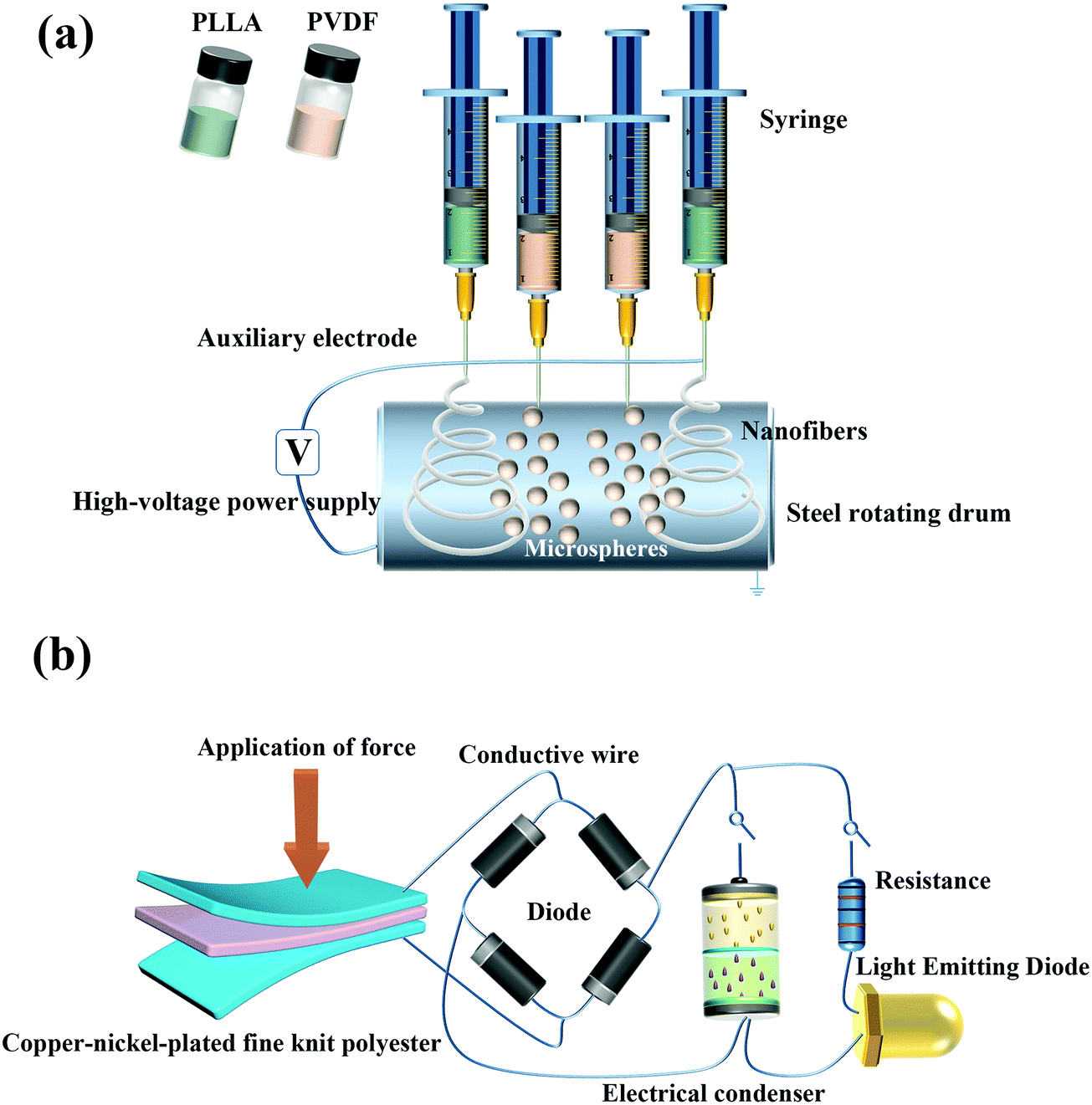 | ||
| Fig. 1 (a) Illustration of electrospinning and electrospraying apparatus. (b) Circuit for charging a capacitor and lighting an LED. | ||
Material characterization
The surface morphologies of the specimens were characterized using field-emission scanning electron microscopy (FE-SEM; Hitachi S-4800, Japan). The piezoelectric constants (d33) of the specimens were measured using a ZJ-6-type quasistatic piezoelectric-constant-measuring instrument (Institute of Acoustics of the Chinese Academy of Science, China).Fabrication of the HTPENG
An area of 2.5 × 2 cm2 was cut from the as-prepared PVDF/PLLA “microspheres@nanofibers” mat (thickness = ∼100 μm). The top and bottom electrodes were then formed by attaching Cu–Ni-plated fine-knit polyester fabric on either side of the mat with an effective contact area of 2 × 1.5 cm2. Finally, conductive copper wires were connected to the top and bottom electrodes.Measurement of electrical properties
The other end of the conductive copper wires was connected to two electrodes of a Keithley 6517B system electrometer (Tektronix Inc., Beaverton, OR, USA), which was used to measure the open-circuit voltage (Voc) and short-circuit current (Isc) of the HTPENG. To convert the alternating current generated by the HTPENG into direct current, a full-wave rectifier was manufactured (Fig. 1(b)).17,18 Currents tuned using four diodes were stored using an electrical condenser.3. Results and discussion
PLLA nanofibers (specimen Y1; average diameter = 0.91 μm; Fig. 2(a)) and PVDF nanofibers (specimen Y3; average diameter = 0.58 μm; Fig. 2(c)) were fabricated using the PLLA spinning solution and the HMW-PVDF spinning solution, respectively. Electrospraying (electrohydrodynamic spraying) is a liquid atomization method that is generally carried out under an electrical force. During electrospraying, the liquid flowing out of a capillary nozzle was dispersed into microspheres under the influence of an electric field.19 Owing to the low viscosity of the LMW-PVDF spinning solution, PVDF microspheres of 4.95 μm diameter (specimen Y2; Fig. 2(b)) were fabricated by electrospraying. Jets formed by different spinning solutions underwent vigorous whipping motions; hence, the diameter of specimen Y4 obtained by the bicomponent spinning of the PLLA spinning solution and the PVDF spinning solution was smaller than that of the PLLA nanofibers (specimen Y1; Fig. 2(a)). Specimens Y5 (Fig. 2(e)) and Y6 (Fig. 2(f)) were fabricated using the low-concentration HMW-PVDF/PLLA spinning solution and the low-concentration PLLA/HMW-PVDF spinning solution, respectively. The low-concentration HMW-PVDF spinning solution was spun into microspheres; however, these microspheres were not uniformly distributed and were inconsistent in size. Moreover, spindles appeared during the spinning of the low-concentration PLLA spinning solution. Specimen Y7 was fabricated via the electrospinning process and the electrospraying process using the same apparatus. PVDF microspheres formed by electrospraying of the LMW-PVDF solution were uniformly distributed on the PLLA nanofibers fabricated by electrospinning of the PLLA solution. The rotational speed was then changed to fabricate specimens Y8 and specimen Y9, and the rotational speed affected the size and distribution of the microspheres.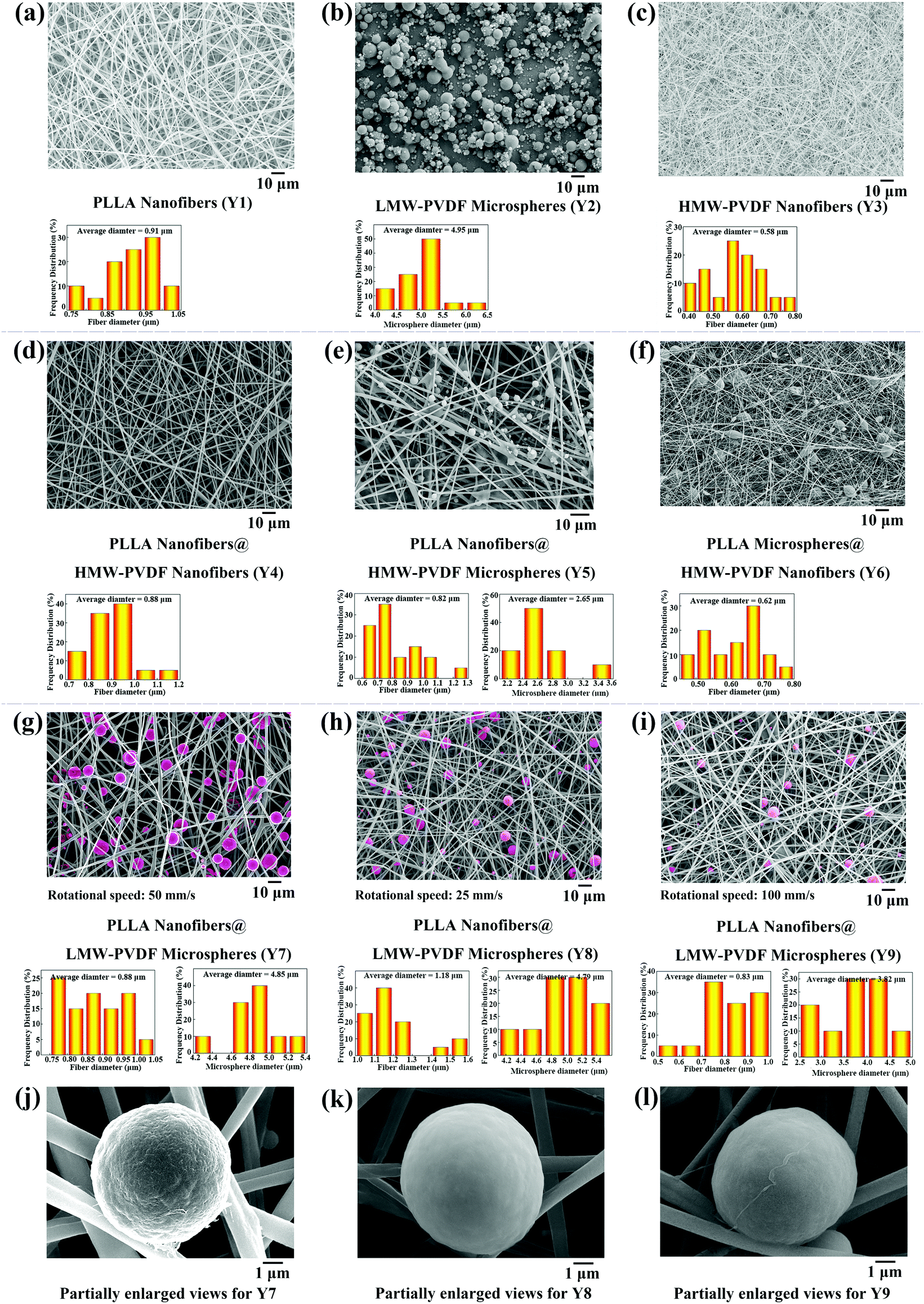 | ||
| Fig. 2 SEM images of specimens (a) Y1, (b) Y2, (c) Y3, (d) Y4, (e) Y5, (f) Y6, (g) Y7, (h) Y8, and (i) Y9. Partially enlarged views of SEM images for specimens (j) Y7, (k) Y8, and (l) Y9. | ||
The piezoelectric properties of the aforesaid specimens were examined, and the corresponding results are shown in Fig. 3 and Table 2. The detailed electrical output properties of the specimens are depicted in S3 (ESI†). In general, all nine specimens and their corresponding HTPENG showed consistency in the piezoelectric properties and electrical output properties. Specimen Y7 yielded the best results (followed by Y4, Y8, Y9, Y3, Y6, Y5, Y1, Y2) with a piezoelectric constant (d33) of 54.2 pC N−1, a short-circuit current (Isc) of 8.066 μA, an open-circuit voltage (Voc) of 35.693 V, and a power density of 525.12 mW m−2, suggesting that the structure and properties of the specimens were adjustable over a wide range. These results are also compared with the data reported previously in the literature, as shown in Table 3. It is clear that the power density of the HTPENG fabricated using specimen Y7 has increased by 5.4 times that of the BaTiO3@PDMS-based HTPENG as reported in the literature13 and 1.82 times that of the BaTiO3@MWCNT@bacterial cellulose paper-based HTPENG reported in the literature.10 In comparison with TENGs and PENGs that were invented recently,14,20–23 the power density of the HTPENG fabricated using specimen Y7 has increased by 1.1-6.9 times.
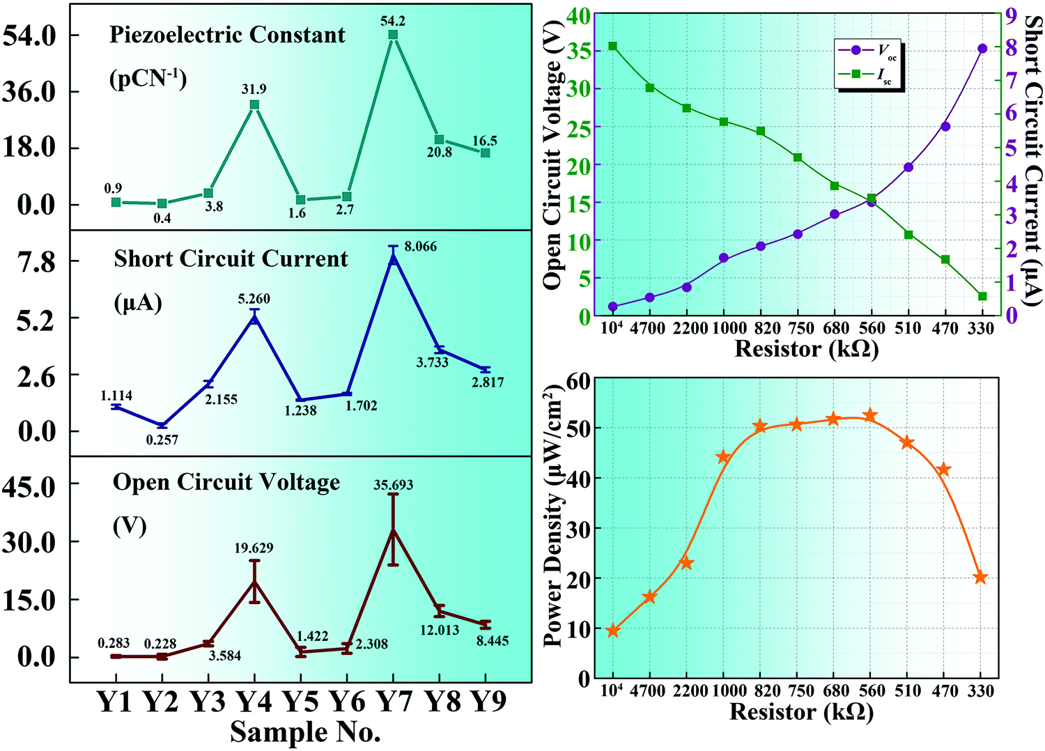 | ||
| Fig. 3 Piezoelectric constant (d33), short-circuit current (Isc), and open-circuit voltage (Voc) of different specimens. The open-circuit voltage and short-circuit current of specimen Y7 under the varied external load resistances. The power density of specimen Y7 under the varied external load resistances. | ||
 | ||
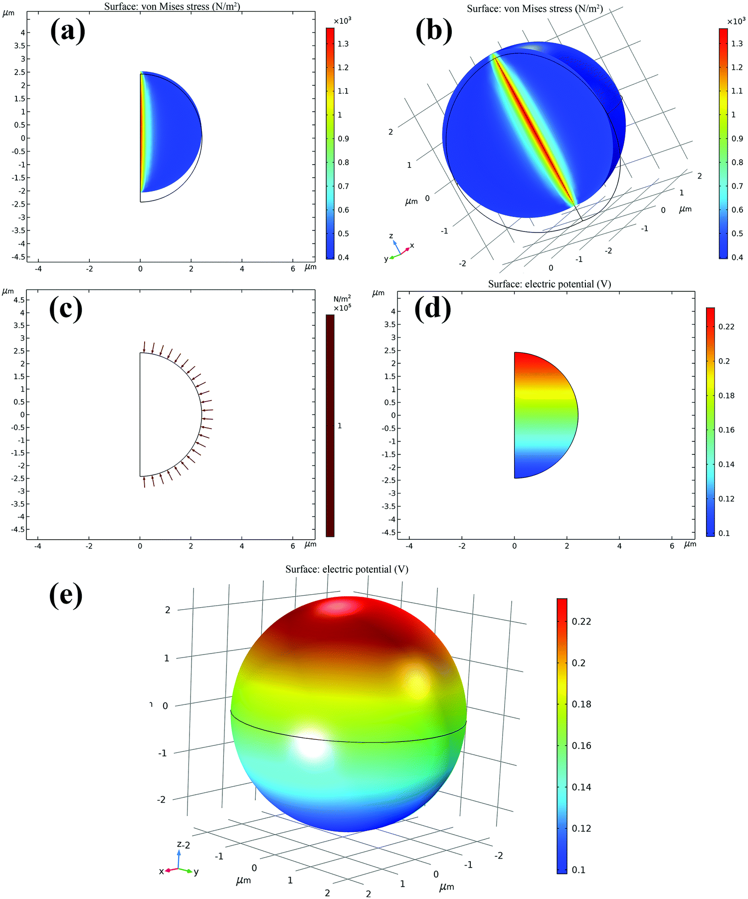
| Fig. 4 Simulated piezopotential distributions for a PVDF nanofiber. (a, b and c) Pressure distribution diagrams. (d and e) Piezopotential distribution diagrams. (f) Partially enlarged view of the piezopotential distribution diagram. | ||
 | ||
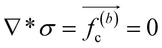
| Fig. 5 Simulated piezopotential distributions for a PVDF microsphere: (a, b and c) Pressure distribution diagrams. (d and e) Piezopotential distribution diagrams. | ||
| Specimen no. | Y1 | Y2 | Y3 | Y4 | Y5 | Y6 | Y7 | Y8 | Y9 |
|---|---|---|---|---|---|---|---|---|---|
| d 33 (pC N−1) | 0.9 | 0.4 | 3.8 | 31.9 | 1.6 | 2.7 | 54.2 | 20.8 | 16.5 |
| I sc (μA) | 1.114 | 0.257 | 2.155 | 5.260 | 1.238 | 1.702 | 8.066 | 3.733 | 2.817 |
| V oc (V) | 0.283 | 0.228 | 3.584 | 19.629 | 1.422 | 2.308 | 35.693 | 12.013 | 8.455 |
| Power density (mW m−2) | 0.59 | 0.53 | 14.56 | 194.57 | 3.32 | 7.40 | 525.120 | 84.51 | 44.88 |
| Materials | V oc (V) | I sc | Measuring instrument | Nanogenerator type | Power density (mW m−2) | Ref. |
|---|---|---|---|---|---|---|
| a PTFE: polytetrafluoroethylene. | ||||||
| PLLA nanofibers@PVDF microspheres | 35.693 | 8.066 μA | Keithley 6517B | HTPENG | 525.12 | This work |
| BaTiO3@PDMS | 60 | 1 μA | Oscilloscope and current amplifier | HTPENG | 97.41 | 13 |
| BaTiO3@MWCNT@bacterial cellulose paper | 18 | 1.6 μA m−2 | Keithley 6514 | HTPENG | 288 | 10 |
| Fingernails@PTFEa | 87.3 | 3.2 μA | Keithley 6517 | TENG | 122 | 20 |
| PTFE@Al | 1100 | 6 mA m−2 | SR570 | TENG | 350 | 21 |
| PLLA@graphene | 33.2 | 2.68 μA | Keithley 6517B | PENG | 76.51 | 14 |
| Fish gelatin nanofibers | 3.8 | 0.45 μA m−2 | Keithley 6485 | PENG | 192 | 22 |
| PDMS@ITO | 1000 | 8 mA m−2 | Keithley 6514 | TENG | 500 | 23 |
Specimen Y7 showed the best properties, which was actually a combination of properties from specimens Y1 and Y2 based on the composition level. However, the individual properties of specimens Y1 and Y2 were found to be the worst. Dipolar orientation and trapped charges are the two main factors contributing to the pyro-, piezo-, and ferro-electricity of polymers.24 The piezoelectric origins of PLLA and PVDF are CO dipoles and CF2 dipoles, respectively. A transient flow of electrons under an external load driven by a piezopotential to balance the Fermi level is the fundamental mechanism of PENGs.25 The triboelectric potential is the main power source for driving TENGs.26 Therefore, the piezopotential and the triboelectric potential are the power sources of an HTPENG consisting of a PENG and a TENG. The Schottky barrier, a third key factor, acts as a one-way diode to ensure the accumulation of electrons in a generator circuit.27
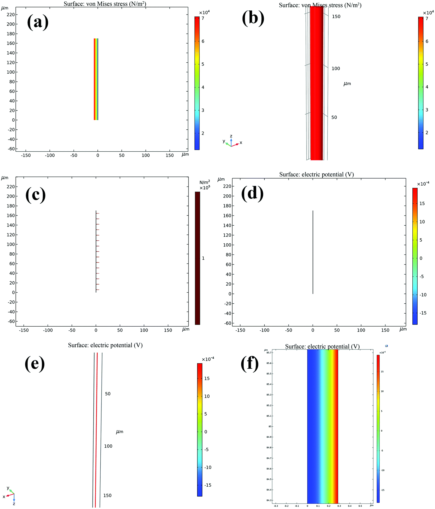
To understand the mechanism for the excellent properties of specimen Y7, finite element simulations were calculated using COMSOL Multiphysics 5.5 software (COMSOL Inc., Sweden). PVDF microspheres in specimen Y7 were formed using LMW-PVDF as the raw material, whereas PVDF nanofibers in specimen Y4 were fabricated using HMW-PVDF as the matrix. Therefore, the piezopotentials of the PVDF nanofibers and PVDF microspheres were simulated and compared.
According to the SEM images shown in Fig. 2, two 3D models according to the sizes of the PVDF nanofibers and PVDF microspheres were established using COMSOL Multiphysics 5.5 under the same pressure intensity of 0.1 MPa. Simulation calculations of the piezopotential involved solid mechanics, the electrostatic effect, and the piezoelectric effect. The main equations used for the simulation calculations were the mechanical equilibrium equation (eqn (1)), the constitutive equation (eqn (2)), the geometrical compatibility equation (eqn (3)), the Gauss equation of an electric field (eqn (4)), and the coupled constitutive equation (eqn (5) and (6)).28,29
 | (1) |
![[E with combining right harpoon above (vector)]](https://www.rsc.org/images/entities/i_char_0045_20d1.gif) is the electric field, and
is the electric field, and ![[D with combining right harpoon above (vector)]](https://www.rsc.org/images/entities/i_char_0044_20d1.gif) is the electric displacement obtained by eqn (2).
is the electric displacement obtained by eqn (2). | (2) |
The compatibility equation is a geometrical constant that must be satisfied using the strain εij.
 | (3) |
| ∇* = ρ(b)e = 0 | (4) |
The Gauss equation must be satisfied for piezoelectric materials.
 | (5) |
 | (6) |
The electric potential distributions of the PVDF nanofibers and PVDF microspheres under 0.1 MPa obtained by finite element simulations are displayed in Fig. 4a–f and Fig. 5a–e, respectively. When the same volume of PVDF nanofibers and PVDF microspheres was used, their corresponding piezopotentials were 0.003 V and 0.12 V, respectively. Under the same conditions, the piezopotential of the PVDF microspheres was much higher than that of the PVDF nanofibers; thus, specimen Y7 showed much better electrical properties than specimen Y4.
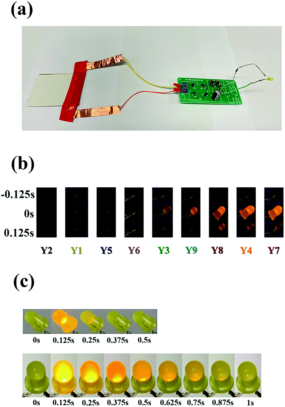 | ||
| Fig. 6 (a) Digital photograph of the full-wave rectifier. (b) Digital photographs of the LED with different specimens. (c) Digital photographs of the LED with different capacitors for specimen Y7. | ||
Specimen Y2, consisting of only PVDF microspheres, manifested the worst properties due to the poor transmission of electrons in it. The connection efficiency between each PVDF microsphere was low, so PLLA nanofibers must act as bridge connections between each PVDF microsphere. Moreover, PLLA nanofibers also played an important role in the triboelectric potential.
The triboelectrification of interactive surfaces is one of the two main mechanisms for triboelectric nanogenerators. The surface charge density also plays an essential role in the electrical output properties of nanogenerators.30 The number of electric charges generated on an interactive surface is an intrinsic property of a material.31 Due to the large composition percentage of fluorine that enables the highest electronegativity among all elements,32 PVDF is one of the most negative triboelectric materials, while PLLA tends to gain positive charges when in contact with most of the materials among the triboelectric series;33,34 therefore, the combination of PLLA and PVDF is beneficial to improve the electrical output properties of TENGs. A large triboelectric contact surface area is favorable for a higher power generation and a lower TENG internal impedance.35 Two 3D models of the same size were developed using 3D Studio Max (3ds MAX) software (Discreet Inc., American) (Fig. 2(d and g)), and the maximum contact areas of PLLA nanofiber with PVDF nanofiber and PVDF microsphere were calculated as 0.00122 μm2 and 0.00423 μm2, respectively. It is observable from Fig. 2(d and h) that the surface roughness of the PVDF nanofibers was lower than that of the PVDF microspheres. The higher roughness can efficiently increase the contact area on the friction material surface, such that more triboelectric charges and performance enhancement of the HTPENG might be expected.36
Furthermore, the combination of PLLA nanofibers and PVDF microspheres can solve a significant disadvantage of electrospun mats. The open, porous 3D structure of an electrospun mat could cause the segmental dissipation of charges when two layers contact each other. Moreover, only nanofibers near the contact surface can collect and deliver charges between two contacting layers, which act as triboelectric layers.37 However, the combination of PLLA nanofibers and PVDF microspheres reduces the porous structure to a certain extent, causing the segmental dissipation of charges. In the case of the combination of PLLA nanofibers and PVDF microspheres, each PLLA nanofiber and PVDF microsphere can collect and deliver charges and play the role of a triboelectric layer, causing nano-level contact electrification.
Piezoelectric materials can generate a large surface charge and electron potential, which could be an effective way to modify the surface-potential difference of triboelectric materials.11 Huang et al.36 confirmed that enhancing the surface charge density of the materials results in a high output performance of the nanogenerators. Concluded by previous finite element simulation results (Fig. 4 and 5), the PVDF microsphere has a greater piezopotential than that of the PVDF nanofiber, which indicates that under similar conditions, the PVDF microsphere can generate more piezoelectric charge on the surface than that of the PVDF nanofiber, which indicates that the surface charge density of the PVDF microsphere is greater than that of the PVDF nanofiber. A major factor determining the output power of a TENG is the density of triboelectric surface charges, which serves as a driving force for induced free electrons.38 Therefore, the triboelectric effect between the PVDF microsphere and the PLLA nanofiber (specimen Y7) is stronger than that between the PVDF nanofiber and the PLLA nanofiber (specimen Y4). This research indicated a synergistic effect of piezoelectricity and triboelectricity: the enhancement of the piezoelectric effect promotes a higher surface charge density of the material, resulting in a stronger triboelectric effect, thereby improving the output performance of the HTPENG. PVDF microspheres with a higher surface charge density, the most crucial factor, lead to better electrical output properties for nanogenerators.
The output properties of the specimens with a single component (Y1, Y2, Y3) are at a low level due to only having the piezoelectric effect. The output properties of the specimen Y4 rank second since the synergistic effect between PVDF nanofibers and PLLA nanofibers is relatively worse than the synergistic effect between PVDF microspheres and PLLA nanofibers. It can be observed from Fig. 2 that, although the specimens Y5 and Y6 have two components, microspheres formed by low-concentration HMW-PVDF and microspheres formed by low-concentration PLLA have common problems of an indeterminate shape, uneven distribution, and different sizes, which lead to a significant decrease in the synergy effect between the microspheres and nanofibers, and the final output properties are unsatisfactory. The specimen Y7 with the unique structure of “PVDF microspheres@PLLA nanofibers” manifested the best electrical output properties among all the specimens, because of its strongest synergistic effect. Owing to the change in the rotational speeds of specimens Y8 and Y9, which, although they have the same components as specimen Y7, the PVDF microspheres became smaller in size, decreased in number, and were unevenly distributed, resulting in an unpromising synergistic effect, ultimately contributing to serious degradation of their properties.
The as-fabricated nine specimens were used to make circuits for charging a capacitor and lighting a LED device (Fig. 6(a and b)). The HTPENG was tapped 90 times within 20 seconds, and the brightness of the LED was observed. Specimens Y2, Y1, Y5, and Y6 with low electrical output properties could not light up the LED within 20 seconds. Specimens Y3, Y9, and Y8 barely light up the LED. However, specimens Y4 and Y7 with high electrical output properties perfectly lit the LED. The 2.2 μF capacitor was replaced with a 220 μF capacitor and the HTPENG made from specimen Y7 was tapped 900 times within 200 s to light up the LED, and it was observed that the LED was lit for a while, demonstrating that the stability of the entire system with a “microspheres@nanofibers” structure was relatively good.
4. Conclusions
An HTPENG was fabricated using electrospun PLLA and electrosprayed PVDF. PVDF microspheres were fabricated via LMW-PVDF electrospraying. The as-prepared PVDF microspheres were uniform in size and evenly distributed on the PLLA nanofibers. Finite element simulation results revealed that the PVDF microspheres had a higher piezopotential than PVDF nanofibers under the same conditions. The PLLA nanofibers act as bridges to create a web network of PVDF microspheres. The fabricated HTPENG with a unique structure of “microspheres@nanofibers” manifested excellent electrical output properties in the field of thin-thickness devices: a short-circuit current = 8.066 μA, an open-circuit voltage = 35.693 V, and power density = 525.12 mW m−2. Finally, a full-wave rectifier was manufactured to light up an LED for a while. The unique “microspheres@nanofibers” structure, discovered for the first time in this research, can greatly improve the electrical output properties of an HTPENG. It is expected that this research can provide new methods to enhance the electrical output properties of nanogenerators and stimulate new ideas for the structural design of nanogenerators in the future.Conflicts of interest
There are no conflicts to declare.References
- K. Dong, X. Peng and Z. L. Wang, Adv. Mater., 2019, 1902549, DOI:10.1002/adma.201902549.
- Z. H. Zhou, L. Weng, T. Tat, A. Libanori, Z. M. Lin, L. J. Ge, J. Yang and J. Chen, ACS Nano, 2020, 14, 14126–14133, DOI:10.1021/acsnano.0c06949.
- W. L. Liu, Z. Wang, G. Wang, G. L. Liu, J. Chen, X. J. Pu, Y. Xi, X. Wang, H. Y. Guo, C. G. Hu and Z. L. Wang, Nat. Commun., 2019, 10, 1426, DOI:10.1038/s41467-019-09464-8.
- X. Shi, S. Zhang and S. Gong, J. Mater. Chem. A, 2020, 8, 8997–9005, 10.1039/D0TA02178D.
- Y. Feng, Y. Zhang, Z. Rahman, D. Wang, F. Zhou and W. Liu, J. Mater. Chem. A, 2016, 4, 18022–18030, 10.1039/C6TA07288G.
- Y. Song, Z. Shi, G. hu, C. Xiong, A. Isogai and Q. Yang, J. Mater. Chem. A, 2021, 9, 1910–1937, 10.1039/D0TA08642H.
- L. Jin, X. Xiao, W. L. Deng, A. Nashalian, D. R. He, V. Raveendran, C. Yan, H. Su, X. Chu, T. Yang, W. Li, W. Q. Yang and J. Chen, Nano Lett., 2020, 20, 6404–6411, DOI:10.1021/acs.nanolett.0c01987.
- K. M. Shi, B. Chai, H. Y. Zou, P. Y. Shen, B. Sun, P. K. Jiang, Z. W. Shi and X. Y. Huang, Nano Energy, 2021, 80, 105515, DOI:10.1016/j.nanoen.2020.105515.
- Y. B. Guo, X. S. Zhang, Y. Wang, W. Gong, Q. H. Zhang, H. Z. Wang and J. Brugger, Nano Energy, 2018, 48, 152–160, DOI:10.1016/j.nanoen.2018.03.033.
- M. Li, Y. Jie, L. H. Shao, Y. L. Guo, X. Cao, N. Ming and Z. L. Wang, Nano Res., 2019, 12, 1831–1835, DOI:10.1007/s12274-019-2443-3.
- T. Huang, Y. J. Zhang, P. He, G. Wang, X. X. Xia, G. Q. Ding and T. H. Tao, Adv. Mater., 2020, 32, 1907336, DOI:10.1002/adma.201907336.
- C. L. Zhao, Q. Zhang, W. L. Zhang, X. Y. Du, Y. Zhang, S. B. Gong, K. L. Ren, Q. J. Sun and Z. L. Wang, Nano Energy, 2019, 57, 440–449, DOI:10.1016/j.nanoen.2018.12.062.
- B. J. Shi, Q. Zheng, W. Jiang, L. Yan, X. X. Wang, H. Liu, Y. Yao, Z. Li and Z. L. Wang, Adv. Mater., 2016, 28, 846–852, DOI:10.1002/adma.201503356.
- X. Li, S. Chen, X. Y. Zhang, J. H. Li, H. H. Liu, N. Han and X. X. Zhang, Energy Technol., 2020, 1901252, DOI:10.1002/ente.201901252.
- J. Zhang, Y. Li, J. Du, X. Hao and H. Huang, J. Mater. Chem. A, 2019, 7, 11724–11733, 10.1039/C9TA01956A.
- O. Yousefzade, S. Valenti, J. Puiggali, H. Garmabi and R. Macovez, J. Polym. Sci., Part B: Polym. Phys., 2019, 52, 222–233, DOI:10.1002/polb.24774.
- A. Jaworek and A. T. Sobczyk, J. Electrost., 2008, 66, 197–219, DOI:10.1016/j.elstat.2007.10.001.
- L. Gu, N. Y. Cui, L. Cheng, Q. Xu, S. Bai, M. M. Yuan, W. W. Wu, J. M. Liu, Y. Zhao, F. Ma, Y. Qin and Z. L. Wang, Nano Lett., 2013, 13, 91–94, DOI:10.1021/nl303539c.
- J. Fang, X. G. Wang and T. Lin, J. Mater. Chem., 2011, 21, 11088–11091, 10.1039/C1JM11445J.
- J. M. Fu, K. Q. Xia and Z. W. Xu, Microelectron. Eng., 2020, 232, 111408, DOI:10.1016/j.mee.2020.111408.
- Y. Yang, H. Zhang, J. Chen, Q. Jing, Y. Zhou, X. Wen and Z. L. Wang, ACS Nano, 2013, 7, 7342–7351, DOI:10.1021/nn403021m.
- S. K. Ghosh, P. Adhikary, S. Jana, A. Biswas, V. Sencadas, S. D. Gupta, B. Tudu and D. Mandal, Nano Energy, 2017, 36, 166–175, DOI:10.1016/j.nanoen.2017.04.028.
- Y. Yang, H. Zhang, Z. Lin, Y. S. Zhou, Q. Jing, Y. Su, J. Yang, J. Chen, C. Hu and Z. L. Wang, ACS Nano, 2013, 7, 9213–9222, DOI:10.1021/nn403838y.
- E. Fukada, IEEE, 2000, 47, 1277–1290 CAS.
- Y. F. Hu, Y. Zhang, C. Xu, L. Lin, R. L. Synder and Z. L. Wang, Nano Lett., 2011, 11, 2572–2577, DOI:10.1021/nl201505c.
- S. M. Niu, S. H. Wang, L. Lin, Y. Liu, Y. S. Zhou, Y. F. Hu and Z. L. Wang, Energy Environ. Sci., 2013, 6, 3576–3583, 10.1039/C3EE42571A.
- C. F. Pan, J. Y. Zhai and Z. L. Wang, Chem. Rev., 2019, 119, 9303–9359, DOI:10.1021/acs.chemrev.8b00599.
- C. L. Sun, J. Shi and X. D. Wang, J. Appl. Phys., 2010, 108, 034309, DOI:10.1063/1.3462468.
- Y. F. Gao and Z. L. Wang, Nano Lett., 2007, 7, 2499–2505, DOI:10.1021/nl071310j.
- S. M. Niu, Y. Liu, S. H. Wang, L. Lin, Y. S. Zhou, Y. F. Hu and Z. L. Wang, Adv. Mater., 2013, 25, 6184–6193, DOI:10.1002/adma.201302808.
- J. Song, B. Yang, W. Zeng, Z. H. Peng, S. P. Lin, J. Li and X. M. Tao, Adv. Mater. Technol., 2018, 3, 1–16, DOI:10.1002/admt.201800016.
- X. He, H. Zou, Z. Geng, X. Wang, W. Ding, F. Hu, Y. Zi, C. Xu, S. L. Zhang, H. Yu, M. Xu, W. Zhang, C. Lu and Z. L. Wang, Adv. Funct. Mater., 2018, 28, 1–8, DOI:10.1002/adfm.201805540.
- S. R. Liu, W. Zheng, B. Yang and X. M. Tao, Nano Energy, 2018, 53, 383–390, DOI:10.1016/j.nanoen.2018.08.071.
- Z. L. Wang, ACS Nano, 2013, 7, 9533–9557, 10.1039/C4FD00159A.
- K. R. Sanjaya, D. Gunawardhana, N. D. Wanasekara and R. D. I. G. Dharmasena, iScience, 2020, 23, 101360, DOI:10.1016/j.isci.2020.101360.
- K. M. Shi, H. Y. Zou, B. Sun, P. K. Jiang and J. L. He, X. Y. Huang, Adv. Funct. Mater., 2019, 30, 1904536, DOI:10.1002/adfm.201904536.
- B. Yu, H. Yu, H. Z. Wang, Q. H. Zhang and M. F. Zhu, Nano Energy, 2017, 34, 69–75, DOI:10.1016/j.nanoen.2017.02.010.
- P. Bai, G. Zhu, Y. S. Zhou, S. Wang, J. Ma, G. Zhang and Z. L. Wang, Nano Res., 2014, 7, 990–997, DOI:10.1007/s12274-014-0461-833.
Footnote |
| † Electronic supplementary information (ESI) available. See DOI: 10.1039/d1ma00464f |
| This journal is © The Royal Society of Chemistry 2021 |