
 Open Access Article
 This Open Access Article is licensed under a Creative Commons Attribution-Non Commercial 3.0 Unported Licence
Advanced developments in nonstoichiometric tungsten oxides for electrochromic applications
Shah
Zeb
ab,
Guoxin
Sun
 ab,
Yong
Nie
a,
Huiyan
Xu
a,
Yu
Cui
*b and
Xuchuan
Jiang
*a
ab,
Yong
Nie
a,
Huiyan
Xu
a,
Yu
Cui
*b and
Xuchuan
Jiang
*a
aInstitute for Smart Materials & Engineering, University of Jinan, No. 336 Nanxinzhuang West Road, Jinan, 250022, P. R. China. E-mail: ism_jiangxc@ujn.edu.cn
bSchool of Chemistry and Chemical Engineering, University of Jinan, No. 336 Nanxinzhuang West Road, Jinan, 250022, P. R. China. E-mail: Chm_cuiy@ujn.edu.cn
First published on 10th September 2021
Abstract
Nanoscale tungsten oxides (WO3/W18O49) are a hot research topic because of their impeccable performance in different fields, such as multi-step responses to one stimulus or selective response to a stimulus under controlled conditions, particularly electrochromic performance and energy saving applications in dynamic controllable smart windows. To satisfy different environments, the transparency and thermal insulation of windows are particularly tailored to reduce energy consumption, thereby decreasing cooling and heating costs. In this review, the nonstoichiometric tungsten oxides (WO3−x) are presented in detail, summarized, and discussed, focusing on various methods for the synthesis of W18O49 and WO3, such as chemical vapor deposition (CVD), physical vapor deposition (PVD), sol–gel, solvothermal, and hydrothermal methods, together with the synthetic strategies for the corresponding thin coatings. Then, the advanced strategies to improve the EC performance of nonstoichiometric W18O49 nanostructures for multi-functionality EC smart windows are discussed. Furthermore, the fundamental mechanisms in coloration/bleaching related to oxygen vacancies, hybridization, elemental doping and surface decoration are explored and discussed in detail. Finally, the key challenges, future developments, and remarks to improve the variability of EC smart windows, such as energy harvesting and energy storing multifunction, coloration enhancement, stability, durability, and reducing toxicity are also highlighted accordingly.
Shah Zeb received his Master's degree from the University of Peshawar, Pakistan, and enrolled as a PhD student in 2017, at the School of Chemistry and Chemical Engineering, Institute for Smart Materials & Engineering, University of Jinan, Shandong, China. He has acquired skills in materials synthesis, advanced chemical techniques to control the morphology, surface chemistry and synthesis of functional nanoparticles, self-assembly of colloids into ordered structures, and low-cost and massive production of micro/nanoscale structures and different characterization techniques. His current research interest focuses on the synthesis and characterizations of tungsten oxide and its composites for gas sensing and electrochromic application in EC smart windows. |
Guoxin Sun currently works as a Full Professor in the School of Chemistry and Chemical Engineering, Institute for Smart Materials & Engineering, University of Jinan, China. He received his PhD degree in 1998 from the Institute of Nuclear Research, Chinese Academy of Sciences. His current research activities focus on solvent extraction; synthesis of new extractants and their extraction removal of precious metals; and organic synthesis and functional nanomaterials. |
Yong Nie is an Associate Professor of Chemistry, Institute for Smart Materials & Engineering, University of Jinan, China. In 2005, he received his PhD in Inorganic Chemistry from the University of Heidelberg, Germany. After a short post-doctoral stay at the University of Colorado Boulder, he started his independent career in the School of Chemistry and Chemical Engineering, University of Jinan, China, in 2006. In 2014 he was a visiting scholar in the Department of Chemistry, University of Utah. In 2018, he transferred to the Institute for Smart Materials & Engineering, University of Jinan. His current research focuses on boron clusters, luminescent materials and stimuli-responsive materials. |
Huiyan Xu works as a Lecturer in the Institute for Smart Materials & Engineering, University of Jinan, China. In 2018, she obtained her PhD degree from the School of Materials Science and Engineering, Xi’an Jiaotong University, China. Meanwhile, she obtained another PhD degree from the Department of Physics, City University of Hong Kong, Hong Kong. Her research focuses on nanostructured functional materials and thin films. She is now studying energy saving EC smart coatings technology, including VO2 thin films. |
Yu Cui currently works as a Full Professor in the Chemistry and Chemical Engineering Department University of Jinan China. She received her PhD degree in 2004 from Shandong University. Her research interests include: (1) synthesis and extraction properties of super affinity chelating agents; (2) separation and purification of rare earths; and (3) adsorption of heavy metals pollutants. She has led four NSF research projects related to the above-mentioned topics. She has published over 60 SCI-indexed journal papers and owns 12 patents that have been authorized. |
Xuchuan Jiang currently works as a Full Professor at the Institute for Smart Materials & Engineering at University of Jinan, China. Since the award of his PhD in 2001 from the University of Science and Technology of China (USTC), he has been devoted to studying the synthesis, self-assembly, and applications of functional nanoparticles. He has published over 140 papers in highly ranked international journals with a total of >8000 citations, giving him an h-index of 45. He has been worked in various academic research institutes since graduating from USTC, including the University of Washington (USA), University of Paris (France), University of New South Wales (Australia) and Monash University (Australia). |
1. Introduction
The growing energy and global environmental issues require advanced, renewable, and sustainable energy resources, especially energy-efficient functional materials. Smart windows are an emerging technology that uses chromogenic materials to tailor the visible light transmission and thermal loads in buildings. Smart windows reduce energy consumption due to their astonishing energy harvesting ability and energy savings compared to the commonly used traditional glass. Therefore, according to the technological challenges, the aim of this green innovation is to build large-area, low-cost, durable, and multifunctional electrochromic (EC) smart windows.It was first demonstrated in 1953 that WO3 thin films can change color via an applied voltage after being immersed in H2SO4.1 Analogous results were achieved by Deb, at the American Cyanamide Corporation in the 1960s2 for WO3-based films, which were subsequently published in 1969 and 1973.3,4 This work was motivated by large companies to produce informative displays and liquid crystal display devices.5 A similar concept was extended to rear-view mirrors in automobiles and industrialized.5 In the 1980s, EC became widely accepted as energy-efficient technology.5–7 In 1984/1985, the name “smart windows” was coined, which become popular, not only to scientists but also soft media and the public. A recent development in chromogenic materials is their energy-saving multi-step application in dynamic switchable smart glasses due to their unique electrochemical properties. A smart window is a dynamically switchable device in which the optical properties of chromogenic materials change upon stimulation, such as electricity, heat, and light, and can be observed. The corresponding technologies are known as photochromic, thermochromic, gasochromic and electrochromic windows, respectively.8–10 Among them, photochromic (PC) materials are the most attractive because they change color when exposed to light and are promising in many applications. The optical transmittance in PC materials drops and returns to its original state without stimulation, such as in sunglasses, lenses, and some plastics.11 In contrast to EC, PC films do not need an external power source. Recently, advancements in this area have been made using WO3 as an active material.12 However, utilizing WO3 in PC smart windows is limited because the switching largely depends on the light intensity and cannot be controlled by the user.11 However, this drawback can be overcome by hybrid photo-electrochromic materials that spontaneously work when exposed to sunlight and also change color or bleached with a supplied electric potential.11,13,14
Thermochromic (TC) materials can respond to changes in temperature with a clear and dark color. TC smart glasses display the automated capability of an optical transmission/reflection with variations in temperature. Operationally, it cannot be a personal preference. Nonetheless, for smart functions, no additional energy is required. Many polymers and small molecules can be activated with thermally dependent reversible reactions or temperature-driven structural rearrangements.15 The most representative material in the group of TC materials is vanadium oxide (VO2) or VO2-based composite materials, which allows the transmission of less heat energy at high temperatures than at low temperatures, and vice versa.16–23 An ultra-transparent coating composed of template-free tunable VO2 hierarchical and honeycomb-like structures showed excellent visible light transparency up to 95.4% at 700 nm with a solar modulation ability of 5.5%.20 The obtained ultra-transparent honeycomb-like V2O5/VO2 film exhibited an enhanced anti-reflective and transmittance performance, which was demonstrated both theoretically and experimentally. The device constructed based on the ultra-transparent honeycomb-like VO2 coating film has potential for energy-saving applications as smart windows. Similarly, vertically aligned VO2 hierarchical nanoplate structures grown on hollow spheroids without any template greatly enhanced the optical properties of VO2 film(s).22 The visible light transmission and solar heat modulation were recorded to be 50% and 11.2%, respectively, with a contrast transmittance of 60 °C at 2500 nm. The film thickness was effective in varying the visible transmittance by lowering the solar optical modulation, i.e., 87.2%, and solar optical sound of 5.3%. The 2D hierarchical nanoplate structure possibly promotes the optical properties for smart windows.
Gasochromic (GC) windows aroused wide interest at the beginning of the 21st century due to their simple, inexpensive layer configuration, and high solar transmittance. The synthesis, characterization, and electrochemical activation of WO3 thin films used as cathodes in EC devices have also attracted interest in gasochromic applications.24 WO3-based thin films are doped or decorated with a catalyst such as Pd or Pt nanoparticles. These films are transparent in the visible spectral range; however, upon exposure to H2 gas, the Pt and Pd nanoparticles in these systems promote the room temperature dissociation of the H2 molecules into hydrogen atoms, which upon reaction with the tungsten oxide support, provoke the coloration (i.e., blue color) of the oxide film.24 The dissociated H+ ions and electrons spillover, and then these ion–electron pairs transfer to the WO3 layer and cause changes in the optical transmittance based on the small polaron transition mechanism.25 However, repeated coloring-bleaching cycles and long-term charge storing usually lead to structural dysfunctions and catalyst poisoning, which increase the switchable time and result in partial gasochromic irreversibility.26 The coloration in a photoemission experiment with a Pt/WO3 system was observed, where Pt nanoparticle-decorated WO3 thin films were prepared by magnetron sputtering at an oblique angle and exposed to H2 gas in situ by near-ambient photoemission spectroscopy (NAPP).24 The formation of Wn+ (n < 6) species, which are associated with oxygen network vacancies, is believed to be responsible for the blue color when exposed to hydrogen. Given that magnesium (Mg) has a high hydrogen storage capacity, which tends to be further improved by hybridizing with various metals and oxides, it has been widely used in H2 storage and switchable mirrors.27 Due to the excellent catalytic property of Nb2O5 for the magnesium-hydrogen reaction, fluorocarbon (FC)/Pd/Mg–Nb2O5 switchable films fabricated via magnetron sputtering and low-temperature inductively coupled plasma chemical vapor deposition technology have demonstrated.28 FC/Pd/Mg–Nb2O5 films exhibit a high dynamic range of luminous properties, excellent optical modulation, and fast H2 adsorption/desorption performance. Similarly, Mg–TiO2 thin films obtained via magnetron co-sputtering can act as the switchable layer in smart windows. Thus, gasochromic switchable mirrors based on Pd/Mg–TiO2 films fabricated via magnetron sputtering demonstrate excellent optical properties, microstructures, and strict structure–function relationships.29
EC materials30,31 have been extensively studied to adjust the transmittance, absorbance or reflectance of visible light and solar heat for energy-saving EC smart windows, information displays, self-dimming rare mirrors for automobiles and aircraft, electronic (e-)papers, electronic (e-)skins, etc.5,6,32–39 To satisfy different environments, the transparency and thermal insulation of windows are particularly tailored to reduce energy consumption, thereby decreasing cooling and heating costs. For this purpose, different types of EC materials have been designed and implemented in EC windows, including tin-doped indium oxide (ITO), aluminum-doped zinc oxide, and especially WO3 nanoparticles, which are electrochromic toward NIR light.40–43 Hybridizing WO3 with traditional transition metal oxides/organic electrochromics for visible light modulation makes it possible to construct dual/multifunction capacities that can independently modulate visible and NIR light. Polymer-based EC materials targeting visible light offer several potential advantages with good absorption properties in a wide range of colors, fast switching speed, and high coloration efficiency, which are usually difficult to achieve with metal oxides.43–45 Based on the design of the donor–acceptor (D–A) structure,46,47 EC polymers with a low onset potential and high reversible-switching stability including conjugated polymers,44,48–50 unconjugated polymers,51 and cross-conjugated polymers have been demonstrated.52–54 Poly(3-hexylthiophene) (P3HT) is a regioregular semiconducting polymer that shows EC modulation under a small electrical bias polarity and acts as an anodically coloring material.55 Given that WO3 is a well-known cathodically coloring material, a hybrid composed of P3HT and WO3 as two active electrochromics demonstrated a dual-band EC performance.55 In the dual EC device, P3HT was used as the anode coloring material and WO3 as the cathode coloring material, and therefore, the transfer of charges from WO3 to P3HT makes it colored, whereas the colors of both materials were bleached in the opposite direction.55
To achieve multiple colors and enhance the functionality of all-in-one-type EC devices, the incorporation of several EC chromophores is inevitable.56 They can achieve the simplest device configuration because of their facile fabrication using versatile solution processes (e.g., spin coating and printing) and easily tunable device characteristics such as transmittance contrast, color, operating voltage, and cyclic stability by varying the concentration of the chromophores57,58 and tuning the electrochemical properties59 or molecular structures60,61 of the redox species. Accordingly, 1,1′-disubstituted-4,4′-bipyridinium salts, which are known as viologens, have been extensively studied because their optical and electrochemical properties can be easily tuned by modifying their substituents. The coloration potential (i.e., reduction potential) of viologens depends on the color. Therefore, uneven color contrast is obtained when a fixed voltage is applied to a device including multiple viologens.62,63 However, self-bleaching occurs even under open-circuit conditions, which is considered to be a weakness of all-in-one EC devices. Polymeric viologens (poly-viologens) have been demonstrated to lower the diffusivity of EC chromophores and minimize self-bleaching.64 Compared with EC devices based on mono-viologens corresponding to the monomer of poly-viologens, EC devices containing poly-viologens exhibit the advantages of lower coloration voltage (−0.55 V) and higher coloration/bleaching cyclic stability (>1500 cycles). In particular, as-designed poly-viologen ECDs show remarkably reduced self-bleaching, resulting in extremely low power consumption (∼8.3 μW cm−2) to maintain the colored state.64 Moreover, compared with common glass, poly-viologen-based EC devices have strong NIR ray absorption capacity, which proves their feasibility as effective heat shutters at low-power consumption.64 EC smart windows utilizing these composite materials can simultaneously control building lighting and heating.
In the OFF state, EC devices are transparent to natural light. When a suitable voltage is applied, electrons are transferred due to the oxidation–reduction reaction, and the EC materials become colored with an optical modulation. Thus, by varying the voltage applied across electrodes modified with EC materials or their composites, they can be switched between “bright and warm”, “bright and cool”, and “dark and cool” modes. Consequently, at a lower potential, windows are in the cooling mode, blocking heat flux but allowing UV light, whereas setting smaller potential switches to dark mode limits both heat rays and UV light. These functional modes facilitate the multipurpose use of windows as follows: (i) operate under different weather conditions particularly with personal preference, (ii) provide better comfort for occupants, and (iii) features associated with energy-storage/harvesting, aseptic/sterile function, aesthetics, privacy/security, high-latitude zones, aircraft, etc.5,32,33,65,66
Energy efficiency in buildings has become a focus, given that 40% of the global energy consumption comes from the urban environment.67,68 Due to the rapid increase in global warming, building cooling is becoming a key problem because every 1 °C rise in temperature leads to a 20% increase in energy consumption.67 Building cooling systems in developed countries account for nearly 50–60% of the total building energy consumption.8,67 The concept of a “zero-energy building” has emerged to control the thermal load via the dynamic optical modulation of “smart” windows.69 Moreover, these Wi-Fi-connected tint-controllable smart glass surfaces are equipped with environmental sensors that can read room occupancy, weather, and sunlight. The emerging smart windows installed in commercial and domestic areas can save ∼170 kW h, i.e., 30% of the total energy consumption annually, which is an important step towards achieving “zero energy buildings”.8,67 The other recent approaches based on energy-saving EC materials and technologies for novel multifunction are published elsewhere.67,68,70–78 Modern commercial buildings in European countries have installed functioning EC smart windows instead of active air conditioning, and approximately 4.5% energy can be saved annually in the USA and Australia.79 Similarly, auto-dimming smart glass and automotive rear-view mirrors have been commercialized.80
Nonstoichiometric metal oxides such as WO3−x, MoO3−x, TiOx, NbOx, NiOx, VxOy, MnOx, and CuxSy have strong light absorption/reflection and thermal insulation properties. In particular, WO3−x-based materials in energy-saving EC devices have application prospects because (i) they possess unusual defects and enormous oxygen vacancies, thus achieving strong adsorption affinity with electrolyte ions, (ii) oxygen vacancies provide free electrons, which increase the electric conductivity, resulting in quick electron transfer from the surface, (iii) strong local surface plasmonic resonance (LSPR) provides strong photoabsorption over a wide range of the NIR region, and (iv) a significant reduction in bandgap results in strong light absorptivity, generating electron–hole pairs.81–86 Because of their unique channel/tunnel-like structures for easy electrolyte ion intercalation, defective structure, low cost, high natural abundance, excellent thermal stability, good compatibility, and high theoretical capacitance, oxygen-deficient W18O49 nanostructures are attractive for application in various chromogenic devices, particularly in EC smart windows.82,83,87,88
The scope of this review is focused on the recent advancements in the synthesis of WO3−x/WO3 nanostructures, EC smart coatings, and future advances in smart windows. Sections 1, 2 and 3 briefly introduce the basic properties and EC mechanism of sub-stoichiometric WO3−x. Section 4 provides an overview of the synthetic methods, film formation, and EC properties. Section 5 discusses the strategies for improving the electrochromism of tungsten oxide, including hybridization, elemental/plasmonic doping, and surface decoration. Section 6 describes the all-in-one solid-state next-generation multifunctional EC window principle and its configuration as a typical example for realization, followed by the conclusions, existing and prospective challenges, and finally future demands.
2. Electrochromism
EC materials coated on a transparent conducting electrode can change their optical properties reversibly and continuously by applying a small electric potential. Thus, the transport of ions can occur between the EC material film(s), ion storage/conducting film(s), and/or ion conducting electrolyte(s). The charges are balanced by intercalated/deintercalated electrons, and then transported through the transparent conductors. Smart films can maintain their physical properties with reversible optical modulation in the open circuit, and their color can be refreshed to a specific intermediate state. If energy storage devices can sense energy changes in predictable patterns, we can quickly determine that energy is running out before these devices stop working, demonstrating a wide range of potentially smart applications. Moreover, energy can be saved by using the energy stored in EC devices. If we need to color an EC device to resist sunshine/protect privacy, charges can be stored inside. If the coloration is no longer needed, the stored energy can be released through an external circuit, providing another way for energy resource utilization.As mentioned, EC films and the complementary counter electrode may have similar optical properties. In a hybrid dual-EC device, two complementary electrodes (working and counter) coated with switchable EC materials have sufficient charge capacity for ion storage, as shown in Fig. 1. These EC devices are promising because the redox reaction that occurs in the active layer is fully compensated and can complete the color changes, resulting in an electrochemically stable battery-type cell. Therefore, EC materials can be (i) cathodic EC materials and (ii) anodic EC materials. Some EC materials that can achieve color from transparent to dark colors by ion-insertion/reduction during cathodic polarization are called cathodic EC materials. Similarly, some are anodic electrochromics, which can achieve a dark color/opaque state from a transparent state under ion-extraction/oxidation during the anodic polarization process. The key variables for evaluating the performance of EC materials are as follows: (i) optical modulation, EC materials should carry excellent optical modulation (100%), i.e., fully transparent in the bleached state and fully opaque in the dark state. (ii) Switching speed, EC materials should reach 90% optical modulation between the coloration and bleaching states. (iii) Coloration efficiency is the key index to evaluate the EC performance. A high coloration efficiency ensures that materials exhibit large optical modulation with low power consumption. (iv) The cycling stability and reliability of EC materials should be maintained for more than 50 years without degradation during use.
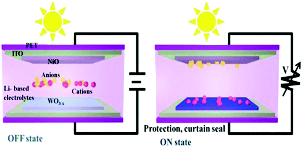 | ||
| Fig. 1 Simplified EC smart window illustration in the colored and bleached state. Electron intercalation through an external circuit into the EC materials (cathode and/or anode), while ions flow through the electrolyte to compensate for the electronic charges. The panel shows sealing with a curtain for protection. | ||
Many inorganic materials such as TiO2, WO3, MoO2, VO2, Nb2O5, Ta2O5, CeO2, NiO, Co3O4, and SnO2;89–92 organics such as Prussian blue; and small organic molecules93–97 including conjugated polymers,96–99 transition metal complexes,34,40,79,100–104 viologens105 and conducting polymers106–109 have been examined recently. The two dominant EC materials are polymers and metal oxides.10 Polymers are excellent candidates for bendable, foldable, and stretchable applications because of their flexible molecular framework interjunctions.10,110,111 Metal oxides possess ultrasmall particle sizes with a large specific surface area and are expected to exhibit excellent EC functionality, possibly due to their short ion diffusion length, easy electrolyte accessibility, excellent coloration efficiency, cyclic stability, and durability. However, metal oxide-based films also have certain disadvantages, such as cracking and degradation, after continuous bending and stretching.
Organic EC materials exhibit controllable color, higher coloration efficiency, and polyelectrochromism similar to that of inorganic EC materials. Particularly, the well-known organic EC materials are organic small molecules, especially viologens, which are the major candidates used in EC display devices. Specifically, viologens are 1,1′-disubstituted-4,4′-dipyridinium salts, with two positive charges, which are colorless in the normal state (V2+), deep-blue in the radical cation state (V+) and reversible.39 When the N-substituents are short alkyl chains (e.g., methyl or ethyl), the colored state including the viologen cation radical shows a blue color. As the alkyl length increases (e.g., heptyl) and the electrolyte has hydrophilic character, the colored species tend to dimerize. Consequently, the colored state is magenta, but the quasi-reversible oxidation of the dimerized viologen cation radical degrades the device performance. Various aryl-substituents have been also reported to obtain other colors such as green. Based on the numerous viologens, multicolor ECDs with EC ion gels have been demonstrated.112 The EC properties of conjugated conducting polymers such as polythiophenes (PT), polydimethylsiloxane (PDMS), poly(vinyl alcohol) (PVA), poly(methyl methacrylate) (PMMA), polyaniline (PANI), polyimide (PI), polypyrroles (PPy), polycarbazoles (PCz), and polyfurans (PF) vary with their molecular structure and bandgap energy. The coloration may be due to the donor moiety, which accelerates the π–π* electronic transition. The HOMO energy level is at a higher energy state. In contrast, the acceptor moiety lowers the LUMO energy level, promoting the charge transfer between the two types of units within the backbone of the polymer in the electrolyte upon electrochemical oxidation and reduction.113 PT, PANI, and PPy have gained intense research interest due to their facile synthetic route, low redox potential and suitable bandgap. The electrochromism in conjugated polymers is tunable with changes in their bandgap, monomer type, conjugation length, side-chain/substitution groups, steric effects, and stereo-regularity. Because of their unique absorptivity and redox reactions in the visible range, they change their electronic structure, optical states, and conductivity under an applied electric current. Metal–organic frameworks (MOFs) are porous materials, and their permanent porosity offers channels for the fast transport of ions, thus enhancing their EC properties.13 However, there are certain challenges9,39,110 that limit the large-scale preparation of organic EC materials as follows:
(i) their multistep synthesis and purification processes,
(ii) use of hazardous organic reagents,
(iii) their photo-electrochemical instability,
(iv) their optical contrast fade-out caused by overoxidation, and
(v) wide range optical modulation in the visible region and lack of control over NIR light.
Recent interest in flexible, stretchable, and foldable devices has been focused on incorporating EC metal oxides in polymers to prepare hybridized materials by carefully matching their refractive index and surface chemistry. The resulting hybrid composites exhibit improved chemical and mechanical properties, enhanced dispersion of nanoparticles, stimuli-responsiveness and provide excellent bendability, stretchability, and foldability.10,39,83,86,98,114 These intrinsic stretchable and transparent conductive electrochromics combine to balance the optical transparency, conductivity, and mechanical stretchability. Focusing on the explosive growth of metal oxides towards EC applications, tungsten, titanium, niobium, vanadium, molybdenum, nickel, copper, manganese, cobalt, and iridium oxides are highly addressed based on their preparation, stoichiometry, particle morphology, composition, and deposition process. Recently, WO3/WO3−x has been demonstrated to be an ideal material owing to its unique EC, electrochemical, and optical properties. The unique detail of this review is the prospective advancement towards next-generation smart windows using W18O49/WO2.72 among the metal oxide (Table 1).
| EC material | EC mechanism and properties | Coloration efficiency (cm2 C−1) | Transmittance contrast | Switching speed (color/bleach (s)) and cycle life (cycles) | Ref. |
|---|---|---|---|---|---|
| WO3−x (amorphous) | Ion insertion, polaron absorption, charge transfer, and Vis and NIR absorption | 125–80 | 56–70% at 550–800 nm | 5 s/2.5 s, 1000 to 4000 | 115–118 |
| WO2.72 assembled on Ag nanowires | Ion insertion, polaron absorption, charge transfer, and Vis and NIR absorption | 35.7 | 58–86% at 550 nm | 2 s/4 s, 1000 | 119 |
| Mesoporous WO3 | Ion intercalation, polaron absorption, charge storage, Vis NIR absorption | 188 | 76% at 700 nm | 0.8 s/0.4 s 1000 | 120 |
| WO3 (crystalline) | Ion intercalation, polaron absorption, charge transfer, free carrier, and Vis and NIR absorption | 42 | 50–70% at 550 nm | Several min, 3000 | 101 |
| WO3·2H2O nanoplates | Pseudocapacitive, polaron absorption, charge transfer, and NIR absorption with transmittance modulation (90.4%) | 322.6 | 63.8% at 550 nm and 90.4% at 1600 nm | 93.7% after 500 cycles | 121 |
| WO3−x/POMs | Ion insertion, polaron absorption, charge transfer, and Vis, NIR selective absorption | 42.31 | 64% at 630 nm and 88% at 915 nm | 26/86, 500 | 122 |
| WO2.72–NbOx on ITO-PET | Ion insertion, polaron absorption, charge transfer, capacitive, and Vis and NIR selective transmission | 30 | — | Mint, 2000 | 123 |
| MoO3–WO3/Ag/MoO3–WO3 | Ion diffusion, charge transfer, and Vis and NIR selective transmission | 70 | 72.9–79.3 at 400–800 nm | 2.7/4.1, 500 | 124 |
| WO3/Ag/WO3 | Ion diffusion, charge transfer, and Vis and NIR selective transmission | 30.5 | 52.5–82.7 at 400–780 nm | 15/22.4, 2500 | 125 |
| NiO | Pseudocapacitive (anodic) polaron absorption, and charge transfer | 30–100 | 68% at 650 nm | 53, 10![[thin space (1/6-em)]](https://www.rsc.org/images/entities/char_2009.gif) 000 000 |
117 |
| Smart window for zero energy building | Capacitive, sensing, plasmon absorption + polaron/charge transfer, and Vis and NIR-independent absorption + reduce toxicity | Infinite | More than 75% at 550–630 nm and More than 95% at IR region | Seconds/less | ? |
| Greater than 50000 |
|||||
| Stand for over 50 years |
3. Nonstoichiometric WO3−x: properties and electrochromic mechanism
3.1. Properties
Tungsten oxide (WO3/WO3−x/WO3·xH2O) is a type of perovskite structure formed of WO6 octahedra connected by W–O–W bonds or water molecule(s) similar to the geometry of rhenium oxide (ReO2). Its electronic structure is composed of oxygen with a filled 2p orbital (valence band) and tungsten with an empty 5d orbital (conduction band).126,127 The WO6 octahedron can be interpreted as a central tungsten metal surrounded by six equidistant oxygen atoms, sharing edges or corners, thus forming a 3D-octahedral crystal structure.128 In the octahedral geometry, there are hexagonal tunnels and trigonal windows (Fig. 3), and the corner sites facilitate the transport of ions. One or two charge-compensated electrons are transferred to the adjacent W-atoms, reducing them to W5+ ions.129 The charge-compensated electrons can be transferred to two neighboring W ions to form a doubly charged W4+ and transition between W4+ to W5+.129–131 The crystal lattice of WOx contains considerable oxygen deficiency sites with partially reduced W5+ species. These sub-oxides with substantial oxygen vacancies become more metalized with an increase in non-stoichiometry and achieve high conductivity. The WO6 octahedral symmetry undergoes tilting and rotation with a change in temperature,132 forming typical monoclinic, hexagonal, orthorhombic and tetragonal crystal symmetries, indicating that the WO3 crystal phases are partially reversible. At room temperature (25 °C), WO3 crystallizes in the triclinic phase, which transforms into other phases upon annealing,132 such as monoclinic II (ε-WO3, <−43 °C) → triclinic (δ-WO3, −43 °C to 17 °C) → monoclinic I (γ-WO3, 17 °C to 400 °C) → orthorhombic (β-WO3, 400 °C to 740 °C) → tetragonal (α-WO3, >740 °C), as shown in Fig. 2. The obtained crystal structures are orthorhombic for W3O8 and W32O84, monoclinic for W17O47, W18O49, W20O58, and W25O73, and tetragonal for W5O14. The reduction reactions of monoclinic WO3 (γ-WO3) forms Magneli phases. Monoclinic WO3 is the most stable phase studied as EC films in EC devices. In this reduction process, with an increase in oxygen vacancies, the position of the WO6 octahedra in the crystal structure changes from corner-sharing to edge-sharing, which split by well-ordered crystallographic shear planes.132 In WO3−x, the edge-sharing WO6 octahedra with channels arrange to form hexagonal and pentagonal tunnels. | ||
| Fig. 2 (a) XRD patterns and crystal structures of (b) WO3 and (c) WO3·2H2O (W, blue; O, red; and H, white).157 (d) Variations in the color of tungsten oxide powders prepared via reduction under a CO atmosphere at different temperatures. (e) XRD patterns of pure tungsten trioxide before reduction and its sub-oxides after reduction under a CO atmosphere. Reproduced with permission.158 Copyright@2017, MDPI. | ||
 | ||
| Fig. 3 Left: (a–g) Unit cells of various WO3−x. The large gray and small red balls represent W and O atoms, respectively. Reprinted with permission.165 Copyright@2010, AIP. Right: (a) Schematic of the transition mechanism from orthorhombic WO3·H2O to hexagonal WO3, (b) crystallographic structure of monoclinic WO3 from layered hydrated WO3via heat treatment process: hydrated WO3 (WO3·2H2O) to monoclinic (γ) WO3. Reproduced with permission.161 Copyright©2017, ACS. (c) and (d) Unit cell orientations of orthorhombic and monoclinic WO3 along the a, b, and c planes,166 and tungsten bronze (MxWO3) (e) cubic (x = 1), (f) tetragonal (1 > x > 0.33),167,168 and (g) hexagonal (x < 0.33) structures.168 | ||
The nonstoichiometric WO3−x was first demonstrated by Glemser and Sauer, where they found that the pure stoichiometric WO3 phase structure could be converted to WO2.9 by introducing oxygen vacancies.133 Therefore, the WO3−x lattice can exhibit a large number of oxygen vacancies, resulting in a variety of non-stoichiometric compounds.79,134 Recent research has focused on the synthesis of sub-stoichiometric tungsten oxide (WO3–x, 0 < x < 1), including W20O58 (x = 2.90), W19O55 (x = 2.89), W5O14 (x = 2.80), W18O49 (x = 2.72), and W32O84 (x = 2.62).135 W18O49 is an n-type material semiconductor with a bandgap of 2.6–3.5 eV. The formation of oxygen vacancies in the WOx lattice affects the Fermi level of tungsten oxide, narrows the bandgap, and increases the conductivity and free carrier electrons.79,133,136 These materials are usually insoluble in all solvents and can be oxidized to stoichiometric WO3 after a long oxidation reaction. Decreasing the particle size increases the bandgap and results in a blue shift and photon absorption.88,136
WO3−x is an interesting LSPR candidate host due to its distinctive properties with outer d-valence electrons. The new discrete energy bands beneath the conduction band (Fig. 4b) are produced by oxygen vacancies.81,137,138 Due to the presence of oxygen vacancies, crystal defects, or insertion of tiny metal ions, strong LSPR with energy comparable to the bandgap energy can induce significant near-infrared absorption properties. The LSPR peak in plasmonic nanoparticles is directly proportional to the square root of the density of free electrons in the particles.139 The LSPR depends on certain factors, such as the particle size, dimensions, structure, shape, and dielectric properties of metals.140 Controlled heat treatment in a weak reducing environment is a facile but effective way to increase the number of oxygen vacancies. The dopants/desired impurities donate their electrons/holes and increase the density of free electron(s) in the conduction band. Meanwhile, the LSPR generates a rigorous local electric field, promoting the photoelectric harvesting application, which has broad application prospects for smart functions in EC windows.141
 | ||
| Fig. 4 Schematic illustration of tungsten oxide in the colored and bleached state. (b) Sketch of the electronic states in WO3 and WO3−x on the y-axis to the left in energy (eV) and the right in potential according to the standard hydrogen potential (SHE) under vacuum. Reproduced with permission.189 Copyright@2017, Elsevier. | ||
The monoclinic W18O49 has excellent stability and can be recovered in the pure phase with substantial oxygen vacancies. W18O49 possesses both the octahedral and pentagonal bipyramidal coordination links of the W with O atoms. Similar to h-WO3, ordered edge-sharing WO6 networks produce three different tunnels/cavities on a crystal plane, such as hexagonal, trigonal, and quadrilateral, to accommodate guest ions during the electrochemical process (Fig. 3).142 Due to its astonishing defect structure and remarkable physicochemical properties, W18O49 has become a potential candidate for application in solar cells,143 photocatalysis,144–147 chromogenic devices,119,139 photothermal agents for cancer treatment,148 supercapacitors and batteries for energy storage,133 and sensors toward various toxic gas molecules because of its distinctive structural faces, ultrathin nature, small particle size, high surface area, reproducible morphologies, crystal defects, and oxygen vacancies.149–154 Hexagonal WO3 (h-WO3) is a metastable phase that has received significant interest in electrochemical applications as an Li+ and Na+ ion host material,155 and its crystal structure is presented in Fig. 3a. In other polymorphs, the octahedral units are organized into a perovskite-like structure. In hexagonal WO3, the WO6 octahedra existing in the form of three- and six-membered rings in the “ab” plane create trigonal cavities and hexagonal windows, respectively, whereas in the “c-axis”, sharing of the axial oxygen results in 4-coordinated square windows.156 These tunnels offer accommodation sites for a large number of guest cations during the electrochemical process. No hexagonal phase was observed during the structural transformation; however, it can be obtained via the dehydration of hydrated tungsten oxides, indicating that the structural transformation can only occur in aqueous media. In addition, it can be converted into a monoclinic phase (Fig. 3b) by annealing at a temperature above 400 °C. The redox reactions of tungsten metal/tungsten oxides in aqueous electrolyte are controlled by various pH-related half-reactions, and possible explanations can be found in the review published by Shinde and Jun.133
Tungsten oxide hydrates (WO3·xH2O) also exhibit properties similar to WO3−x nanostructures. They can be classified into subclasses based on the number of water molecules present in their crystal lattices as follows:
(i) WO3-dihydrate (WO3·2H2O),
(ii) WO3-monohydrate (WO3·H2O), and
(iii) WO3-hemihydrate (WO3·1/2H2O)/WO3·0.33H2O.
WO3·2H2O has a stratified layered structure composed of a WO5(OH)2 layer sharing corners and the other water molecule is found in between the layers. Hence, it can be facially exfoliated into thin 2D nanosheets.81,159 WO3·H2O is composed of highly distorted WO5(OH)2 units sharing corners and is coordinated by five oxygen atoms and one H2O molecule. As shown in Fig. 3e, it is believed that the crystal structure of WO3·1/2H2O resembles a cubic pyrochlore type, where the water molecules are present in its tunnels.160 The inter-layer expansion can significantly reduce the ion diffusion energy barrier, ultimately improving the ion diffusion kinetics. Furthermore, the structural water molecules confined in the nano-interlayer spaces facilitate efficient proton transfer and induce a battery-to-pseudocapacitor transition in electrode materials.161,162 The interlayer water molecules can improve the intercalation capability of EC ions, which is significantly important in attaining superb NIR electrochromism in EC devices. Accordingly, Wang et al.163 demonstrated hydrated WO3 and studied the influence of water molecules in decreasing the energy barrier of ion diffusion and improving the ionic flux in the WO3 crystals. They found that WO3·2H2O exhibited a good NIR extension with a large transmittance modulation (90.4%), high coloration efficiency (322.6 cm2 C−1), and high cyclic stability (maintaining 93.7% after 500 cycles), with good solar heat maintenance capability. Li and coworkers164 reported an EC hybrid material using WO3·H2O nanosheets and a Persian-white film on FTO substrate as an asymmetric electrode. The film had an optical modulation of 61.7%, response speed of 1.84/1.95 s, coloration efficiency of 139.4 cm2 C−1, and cyclic stability of 82%.
The optical properties of WO3−x can be measured by absorbing photon energy, which excites electrons from the valence band (occupied state) to the conduction band (empty state) and generates electron–hole pairs.169 The absorption coefficient (α) evaluated from the spectral transmittance, T(λ), and reflectance, R(λ), is given as eqn (1).
| α(λ) = 1/dln[(1 − R(λ))/(T(λ))] | (1) |
| ε ∝ ∞(ε − Eg)η | (2) |
Because of the reduction in particle size (quantum confinement effect), the bandgap becomes wide, resulting in light emission at shorter wavelengths.173 Nonetheless, the structural defects and oxygen vacancies in WO3−x narrow the bandgap due to the defective band below the conduction band. The high concentration of oxygen vacancies in WO3−x extend the defective band into the conduction band. This forms a degenerate semiconductor, which shifts the Fermi level upward, achieving metal-like conductivity, and thus highly improves the electrochromic, electrochemical, photocatalytic, and photochromic properties.171 The color of WO3 films changes from light-yellow to light-greenish and WO3−x changes to dark blue, which shows a blue shift. Broad absorption bands appear in the red to NIR region and blue-green region. The absorption bands at these specific wavelengths make WO2.72 light green, where the additional absorption bands are due to the transfer of electrons from W6+ to W5+.172 The excess electrons can be localized, which are known as small polarons, or transferred to adjacent W ions.174 The intercalated electrons may occupy the empty d-bands and develop a new electronic transition that is delocalized on crystalline WO3 or localize on the metal sites in an amorphous form and perform polaronic absorption. Amorphous WO3−x exhibits a disordered structure, indicating the presence of broken bonds with variable bond lengths, bond angles, and coordination. In WO3−x, the localized states are found closer to the oxygen vacancies or tungsten atom, and thus the electrons and/or charge compensating ions can easily jump within the localized states.136,169,175
3.2. Electrochromic mechanism
The EC properties mainly depend on the particle size, dimensions, aspect ratio, crystallinity, porosity, thickness, and reversibility of films, together with their capability to accommodate guest ions (H+, Na+, and Li+).13,88,176 The coloration mechanism depends on the nature and behaviors of materials. In crystalline tungsten oxide films, their coloration is attributed to the Drude-like absorption of delocalized/free electrons, similar to the behavior of heavily doped metal oxides with ionized impurities.177 In amorphous tungsten oxide films, the optical absorption is caused by the electron exchange/polaron-to-polaron transition between adjacent W atoms (W6+, W5+, and W4+ states), and the inserted electrons are localized in the W5+ sites and polarize their surrounding lattice to form small polarons.178 Moreover, compared to crystalline films, amorphous WO3 films show a better coloration efficiency, which increases with an increase in oxygen vacancies.179 However, amorphous tungsten oxide films show poor stability because of their irregular atomic distribution.88W18O49 is a promising EC smart material that changes color from clear to blue, dark-blue, and transparent with a faradaic charge. When protons/lithium ions intercalate and externally powered electrons are inserted into the tungsten oxide film, the transmissivity of the electrodes drops from 91.3% to 15.1% during charging.129,180 Two types of redox reactions occur upon voltage bias as follows:181 (a) a charge transfer process at the material-electrolyte interface, i.e., surface-dependent process and (b) diffusion controlled redox reactions within the material lattices, i.e., ion-diffusion dependent process. The intercalated cations exist in the channels formed by the WO6 octahedra or react with the bridging oxygen of the host156 by breaking the W–O–W networks and generating new W![[double bond, length as m-dash]](https://www.rsc.org/images/entities/char_e001.gif) O bonds.128,182 Thus, the coloration (tungsten bronzes, HxWO3/LixWO3 formation) is due to the reaction of cations with WO groups by forming colored W5+–OH states.181 It is assumed that cations can react with the bridging oxygen at a low concentration of inserted charges. However, at a high concentration, they can also react with W–O.128,181,183 Raman spectroscopy results show that the interaction between oxygen vacancies and Li+ ions improves the coloration efficiency of WO2.72 films.129,136,179 When the applied voltage polarity is reversed, the Li+ ions de-intercalate and the film is bleached. These redox dynamics demonstrate that tungsten oxide can be transformed from a transparent state to an absorbent state to store electric energy.
O bonds.128,182 Thus, the coloration (tungsten bronzes, HxWO3/LixWO3 formation) is due to the reaction of cations with WO groups by forming colored W5+–OH states.181 It is assumed that cations can react with the bridging oxygen at a low concentration of inserted charges. However, at a high concentration, they can also react with W–O.128,181,183 Raman spectroscopy results show that the interaction between oxygen vacancies and Li+ ions improves the coloration efficiency of WO2.72 films.129,136,179 When the applied voltage polarity is reversed, the Li+ ions de-intercalate and the film is bleached. These redox dynamics demonstrate that tungsten oxide can be transformed from a transparent state to an absorbent state to store electric energy.
The ion insertion and extraction in WO3 films can be shown as eqn (3)–(5):
Cathodic reaction,
| [WO3−x + H+ + Xe−]bleached → [HxWO3−x]colored | (3) |
| [WO3−x + Li+ +Xe−]bleached → [LixWO3−x]colored | (4) |
| [Ni(OH)2]bleached → [NiOOH + H+ + e−]colored | (5) |
The removal of the oxygen atom (oxygen vacancy) from the WO3 structure produces two additional electrons that can be paired in a single spin state (closed-shell) (Fig. 4b) or an unpaired triplet spin state. Furthermore, single/two electrons can be transferred to nearby W atoms, resulting in W5+ and W5+–W5+ centers, respectively. The formation of an oxygen vacancy changes the W–W bond distance across the O vacancy sites. Thus, the W–O bond length and bond angles in the crystal change as the bonded orbitals split, leading to the hybridization of the W5d and O2p orbitals. The inserted electrons and ions diffuse and localize on the tungsten atoms, reducing some of the W6+ to W5+ states. Because of the absorption of photons, the inserted electrons gain sufficient energy, which can be transferred to the adjacent sites184 or oxygen vacancies, indicating that oxygen vacancies have a significant impact on both the photochromic and EC properties.130,131 The W4+ state is considered energetically unfavorable, although XPS results prove the existence of W4+ ions.136,186 However, XPS is surface sensitive and is not consistent about the bulk state of different tungsten oxide films.186 The most favorable condition is the creation of a double charge vacancy and two W5+ ions. The transfer of charges between two sites is represented by “i” & “j”, as given in eqn (6).
| Wi5+ + Wj6+ + photon → Wi6+ + Wj5+ | (6) |
4. Synthesis and film fabrication strategies of WO3−x/WO3
Substantial efforts have been dedicated to synthesizing WO3 nanostructures with different morphologies, sizes, and dimensions (0D, 1D, 2D, and 3D), as displayed in Fig. 5. To date, tungsten oxide particles have been synthesized by varying the synthetic conditions and technologies, which greatly affect their size, morphology, and functional applications. According to the relevant reaction media, the techniques can be grouped into two main categories, i.e., gas-phase technologies and wet-chemical synthesis methods. Gas-phase technology is classified as plasma sputtering,190 chemical vapor deposition,191 and physical vapor deposition. Wet-chemical synthesis includes Langmuir–Blodgett deposition,192 electrophoretic deposition,193 electrospinning,194 and hydrothermal195 and solvothermal synthesis. Similarly, spray-coating, inkjet printing, spin-coating, roll coating, screen printing, and layer-by-layer self-assembly have also been employed.196 However, the material synthesis and film fabrication processes are still challenging to adopt on a large scale. These technologies will be reviewed in this section. | ||
| Fig. 5 Schematic illustration of the design of WO3−x/WO3 nanostructures with different shapes/dimensions.197 0D nanoparticles, 1D nanowires and nanotubes, 2D thin layers, and 3D porous nanostructure. Reproduced with permission.198 Copyright©2019, ACS. | ||
4.1. Gas-phase deposition methods
Brescacin et al.201 developed phosphorus (P)-doped amorphous WO3 films via CVD processes using volatile, low-melting P-doped tungsten carbonyls. The P-doping preserved the amorphous nature of the material and deposited film, even upon calcination at high temperatures. The tiny amount of dopant released by the precursor during its decomposition was sufficient to inhibit the crystallization of tungsten oxide on the matrix. The films deposited on common glass displayed remarkable EC performances with the maximum coloration efficiency of 66 cm2 C−1. Ou et al.202 synthesized tungsten(VI) oxo-complexes of the type WO(OR)3L having partially fluorinated alkoxide and/or chelating ligands (Fig. 6). The thermal decomposition behavior and mass spectrometry (MS) of selected examples were studied. With WO(OC(CF3)2CH3)3 as a single-source precursor, tungsten oxide (WOx) was deposited via CVD and AACVD and compared. The obtained deposited coatings exhibited different crystallinity, structures, and morphology (nanowires, nanoplates, and nanocubes). These variations in morphology demonstrated that the solvent used during AACVD controls the growth of the film. The obtained results suggested that the materials deposited by both deposition methods allow not only the procedure to be scaled up, but also have the potential to generate the formation of a film on a wide area with EC properties.
 | ||
| Fig. 6 (top) Plane-view SEM images of deposits grown on Si〈100〉 at 500 °C, 450 °C, 400 °C, and 350 °C from the precursor via (a) AACVD and (b) CVD. Reproduced with permission.202 Copyright@2019, ACS. (c) High-magnification SEM images of γ-WO3 film deposited via the HW-CVD (hot wire) method. Reproduced with permission.203 Copyright@2017, Wiley-VCH. (bottom) Deposition at different times. Top view (a) over 5 min, (c) over 60 min, and (e) over 60 min with 48 h of additional substrate heating during and after deposition. (b, d and f) View of fractured cross section of the corresponding films. All scale bars represent 500 nm. Reproduced with permission.204 Copyright@2010, Wiley-VCH. | ||
Studies emphasized that MoO3 and WO3 have similar EC properties, and thus the APCVD method can be used solely to obtain a film composed of either Mo-doped WO3 or mixed Mo–W oxides via the pyrolytic decomposition of metal carbonyls.205 The visible light transmission of the film deposited on ordinary glass was about 80%, while that on conductive glass (e.g., SnO2:Sb/glass) was about 60%. It is also found that after annealing, the optical transmission of the single oxide films improved, while that of the mixed oxide films slightly decreased. The mixed oxide showed deep-blue coloring only at the cathode, minimizing the visible-light transmittance. Similarly, excellent reversibility with an optical modulation of about 30% was obtained. Numerous reports based on mixed Mo–W oxides have been published.206,207
PVD is comprised of four steps as follows:
(i) evaporation of materials deposited by high energy sources (e.g., electron beam/ions that evaporate atoms from the surface);
(ii) transport of the vapor to the substrate to be coated;
(iii) the reaction between the metal atoms and the appropriate reactive gas (such as oxygen, nitrogen, and methane) during the transport stage; and
(iv) deposition of the coatings on the surface of the substrate.
The PVD method has several advantages including (i) PVD thin coatings demonstrate better properties compared to the substrate materials; (ii) all types of inorganic materials and some types of organic materials can be used; and (iii) the procedure is more environmentally benign than several other techniques, e.g., simple electroplating. Meanwhile, the PVD method also has certain disadvantages, including (i) problems with coating complex shapes; (ii) high cost and low output; and (iii) complexity of the process.
Zhang et al.208 demonstrated the growth of a WO3–WS2 bilayer hybrid with WO3 monolayer species attached on the surface of large-size WS2 monolayers, as shown in Fig. 7a–d. The optical analysis showed that the photoluminescence quantum yield (PLQY) of the as-prepared WO3–WS2 hybrid was excellent and could reach 11.6% higher PL than that of the bare WS2 monolayers, which is about 13-times greater than that via the mechanical exfoliation of WS2 (Fig. 7e–g). The improved PL enhancement mechanism can be investigated by carrying out time-dependent optical measurements. The generation of WO3–WS2 hybrid structures with ultrahigh PLQY can provide an efficient method for developing highly effective 2D integrated photonic applications. Hadifakoor et al.209 fabricated a DMD skeleton of WO3/Ag/WO3 thin films with various thicknesses through the PVD approach via electron-beam evaporation under the vacuum at pressure of 10−5 torr and calcination temperature of 100–400 °C. The structural and optical properties of the nano-multilayer composites structures were studied in heat mirror applications. Nanosized Ag layers with thicknesses of 10 nm, 12 nm, and 14 nm were deposited on monolayer WO3 films. Atomic force microscopy (AFM) showed the morphology of the individual layers, indicating that a smoother layer can be achieved after annealing at 300 °C. Ellipsometry analysis was performed to examine the bilayers, thickness of the Ag film layer, and inter-connectivity between the WO3–Ag–WO3 layers. There was almost no interference among the WO3–WO3 layers in the samples with Ag thicknesses of 12 nm and 14 nm. The efficiency of the heat mirrors was evaluated according to their optical characteristics and best performance. Recently, Hoseinzadeh et al.209 studied a WO3 and Ag composite deposited via the layer-by-layer (LbL) PVD method as an EC electrode on an FTO glass substrate. Nano-sized silver noble metal can behave as an electron-trap center, which enables the departure of charges. The electrochemical and optical properties were examined through CV and UV-visible absorption experiments, which showed that heating the deposited film at 200 °C can provide much better conductivity (90 mA) and transmittance change (ΔT = 90% at a continuous switching step), endowing WO3–Ag–WO3–Ag with excellent EC properties. Esmail et al.210 demonstrated amorphous WO3 smooth films thinner than 200 nm, which exhibited an excellent coloration efficiency with a switching speed in the order of seconds.
 | ||
| Fig. 7 (a and b) Schematic of the synthetic process and 3D representation of the WO3–WS2 heterostructure. (c and d) Typical optical image of (c) partially covered and (d) completely covered WO3–WS2 heterostructures. The inset in (c) shows the SEM image of the area within the red box. (e–g) AFM images of (e and f) partially covered and (g) completely covered heterostructures. The insets show the corresponding height profile. Reproduced with permission.208 Copyright@2019, ACS. | ||
4.2. Wet-chemical synthesis methods
The gas-phase deposition of coatings is a highly pure and efficient route for the fabrication of WO3 films. However, the required instrumentation is very complex and expensive. Conversely, solution-based particle synthesis and film formation are cost effective, controllable, and high yielding, which provide an alternative reliable route for the production of smart coatings, reflective displays, and sensors.211The sol–gel method is attractive due to the following reasons:
(i) it provides an easy route for the preparation of metal oxide microstructures and mixed oxides with a controlled composition and homogeneity,
(ii) processing produces an amorphous hydrogel, which is better than crystalline films due to its excellent elasticity,
(iii) can reform volume changes caused by redox reactions, and improve conductivity,
(iv) films can well adhere to ITO/FTO films and be processed at ambient pressure, and
(v) deals with a new deposition method of WO3-based coating on a large scale.
In 1984, Chemseddine et al.224 first reported the results of a sol–gel EC WO3 film, which was then subjected to different sol–gel processes for the production of pristine WO3 and mixed oxides. The coloration efficiency values compared to the reported sol–gel films were 70 cm2 C−1 (at 685 nm) and 223–167 cm2 C−1 (at 800 nm)225 compared to 115 cm2 C−1 (at 633 nm) for the amorphous films226 produced via thermal evaporation and 42 cm2 C−1 (at 650 nm) reported for sputtered polycrystalline films.227–229 The advantage of the sol–gel technique is its capability to generate various mixed oxides from a variety of hybrid mixtures with controlled compositions.230–240 Nguyen et al.241 used the sol–gel spin coating process and further annealing to form amorphous EC WOx thin films. The precursor solutions were prepared from ammonium metatungstate hydrate ((NH4)6[H2W12O40]·4H2O) and dimethylformamide (DMF) to produce a smooth and transparent amorphous WOx film via spin-coating followed by calcination in air at 250 °C for 2h. The obtained EC film exhibited excellent stability over 4000 switching cycles with a coloration efficiency of 125cm2 C−1 and color/bleach times of 5/2.5 s. Amorphous WOx film-based devices are impeccable for next-generation smart windows and other electronic display devices. Recently, Azarian et al.242 explored amorphous electro-photochromic films formed via the in situ sol–gel synthesis of 10 wt% WO3 and 30 wt% LiClO4 (denoted as GLi30W10) in a gelatin/lithium cosolvent mixture (Fig. 8d–f). The transparent single-layer film was flexible and adhesive, active under UV radiation with a photo-response time of 30s, and gradually reversed once the UV source was blocked. Besides, in the presence of a conductive ion storage anode, the film on ITO glass exhibited an excellent EC response. The EC device configured with ITO/GLi30W10/NiO/ITO achieved a coloration efficiency of 51.54cm2 C−1 and fast color-bleach response times (2 s/1 s). Jittiarporn et al.243 prepared hybrid MoO3–WO3 thin films on ITO glass via a sol–gel dip-coating process (Fig. 8). The formation of the film could be influenced by the calcination temperature, the concentration of MoO3 (0–10%), and the copolymer template of Pluronic P-123 triblock (0–20% w/v). The lowest amount of 5% MoO3-95% WO3 films without the use of the template and 200–300 °C annealing resulted in a high CE, excellent cycling stability, and low response time. The surface roughness and low crystallinity of the films were thought to be attributed to their enhanced EC features. Amorphous mesoporous WO3 with a pore size in the range of 20–30 nm was fabricated via evaporation induced self-assembly and used as an electrochromic supercapacitor (ECS).120 The resultant device based on ECS exhibited excellent optical modulation (76% at 700nm), ultrafast switching speeds (0.8s for coloration and 0.4s for bleaching), and a high areal capacitance (2.57 mF cm−2), even at a high current density (1.0mA cm−2).
 | ||
| Fig. 8 Surface morphology of the 5% MoO3–95% WO3 film annealed at (a) 300 °C and (b) 400 °C. (c) Transmittance spectra. Reproduced with permission.243 Copyright@2017. Elsevier. (d) Film containing 30 wt% LiClO4 and 10 wt% WO3 (sample denoted as GLi30W10), (e) tungsten map and (f) chlorine and tungsten distribution mapping. (g) Transmittance spectra of free-standing films and (g) optical images of colored and bleached states. Reproduced with permission.242 Copyright@2020, Wiley-VCH. | ||
Sun et al.244 prepared mixed molybdenum-tungsten oxides with different stoichiometries (MoxW1−xO3, 0 < x < 1) via sol–gel deposition from peroxo-polymolybdotungstate solutions onto FTO glass substrates. The MoxW1−xO3 films were annealed at 450 °C. The transmittance modulation of the mixed oxide films was improved compared to the pristine WO3 film and no broadening of spectral modulation was observed. Kharade et al.231 also employed a similar method to prepare MoO3 mixed WO3 thin films via hybrid physicochemical synthesis involving the microwave-assisted sol–gel preparation of WO3 and vacuum evaporation of MoO3 on an FTO glass substrate. Similarly, a mesoporous WO3–TiO2 composite film was fabricated via a sol–gel-based two-stage dip-coating technique on ITO glass, and subsequently annealed at 450 °C, 500 °C, and 600 °C.245 The composite film calcined at 600 °C contained orthorhombic WO3 and anatase TiO2. Mesoporosity was achieved in the film by employing silicates as templates. Mixed hexagonal and monoclinic phases were obtained upon calcination at 450 °C and 500 °C. The results show that nanocrystal anatase TiO2 can stabilize the orthorhombic WO3 phase by calcination at 600 °C. The mesoporous dye-sensitized WO3–TiO2 composite film calcined at 600 °C showed an optical modulation of 51% in the NIR region. In contrast, the devices examined for the composite layers annealed at 450 °C and 500 °C displayed a moderate optical modulation of 24.9% and 38%, respectively.
| Technology | Methods | Sub-method | Materials | Morphologies | Coloration efficiency, color/bleach response and cyclic stability (cycles) | Ref. |
|---|---|---|---|---|---|---|
| Mechanochemical process (Ball milling) | NaxWO3 (bronze) | Nanoparticles | 246 | |||
| Magnetron sputtering | WOx | 46.9 cm2 C−1, 7.8/117.8 s | 247 | |||
| Gas-phase technologies | CVD/PVD | R.F. sputtering | WO3 | 46.45 cm2 C−1, 8.33/4.16 s | 248 | |
| R.F. sputtering | WO3+x | Granular | ∼213 cm2 C−1, 5000 | 249 | ||
| Thermal vapor deposition | WO3−x | Nanorods | 250 | |||
| HIPIMS | WO3/Ag/WO3 | 30.5 cm2 C−1, 15/22.4 s, 2500 | 125 | |||
| APCVD | WO3−x | Nanowires, nanoplates | 200 | |||
| Wet-chemical technologies | Hydrothermal/solvothermal | WO2.72 | Sub-micro fibers | 251 | ||
| WO2.72 | Nanodots | 154 cm2 C−1, 1/1 s | 252–255 | |||
| WO2.72 | Nanocrystals/particles | 124.5 cm2 C−1, 1.9/2.8 s, 1000 | 139 and 256 | |||
| WO2.72 | Nanowires | (—) | 135 | |||
| WO2.72 | Nanowires assembled | 35.7 cm2 C−1, 2/4 s, 1000 | 119 and 257 | |||
| WO3 | Nanorods/Nanowires arrays | 102.8 cm2 C−1, 25.2/18 s, 7.6/4.2 s, 3000 | 229 and 258 | |||
| WO3 | Nanoparticles | 151.9 cm2 C−1, 1.3/1.7 s | 259 | |||
| Nanofibers | 109.6 cm2 C−1, 2.7/7.9 s, 4000 | 260 | ||||
| WO3 | Particles | 178.7 cm2 C−1, 1.9/2.5 s, 5000 | 261 | |||
| WO3 | Nanoflakes/sheets | 55.6 cm2 C−1, 5.2/2.2, 3000 | 262 | |||
| WO2.72 | Nanowires/Nanotrees | 75.35 cm2 C−1+, 2.64/7.28 s, | 263 | |||
| WO2.72 | Nanoneedles | 150 cm2 C−1, 500 | 264 | |||
| WO2.72 | Nanobelts | (—) | 265 | |||
| WO3 | Nanobricks | 39.24 cm2 C−1, 9.7/6.9 s | 266 | |||
| WO3/NiO | Nanoporous structures | 85.9 cm2 C−1, 21.76/4.54 s | 267 | |||
| WO3·H2O, WO3·2H2O | Nanoplates | 384.6 cm2 C−1, 322.6 cm2 C−1, 500 | 163 | |||
| WO2.72/POMs | Nanowires | 42.31 cm2 C−1, 52/26 s, 500 | 122 | |||
| WO3–TiO2 | Hierarchical nanostructure | 128.3 cm2 C−1, 6 s, 1000 | 268 | |||
| WOx–NbOx | Nanowires | |||||
| WO2.72 | Mesoporous | 80.5 cm2 C−1, 5.3/3 s | 70 | |||
| WO2.72 | Mesoporous | 46.9 cm2 C−1, 7.8/117 s, 8 | 247 | |||
| Sol–gel | Spin coating | WOx | 125 cm2 C−1, 5/2.5 s, 4000 |
241 | ||
| Dip coating | WO3 | Mesoporous | 35.8 cm2 C−1, 16/30 s | 269 | ||
| Electrodeposition | Ag–WO3 | Nanowires composite | 45.3 cm2 C−1, 12/2 s | 270 | ||
| Inkjet printing | WO3/TiO2/WOX | 480 cm2 C−1, 3.3/2.8 s | 271 | |||
| WO3-PEDOT:PSS | composite | 68.8 cm2 C−1, 2.4/0.8 s, 10000 |
272 | |||
| Langmuir–Blodgett | WO3 | Nanobundles | 41.8 cm2 C−1 | 273 | ||
| Electrostatic force-assisted printing | WO3 ink | WO3 powder | 51.5 cm2 C−1, 65.5% at 700 nm, 25 s/24 s | 274 | ||
| Spray pyrolysis | ||||||
| Pulsed electrochemical deposition | WO3 | Poros films | 118.3 cm2 C−1, 6/2.7 s | 275 | ||
| Electrochemical deposition | WO3 | Nanorods/nanoparticles | ∼90 cm2 C−1, 3/2 s | 185 | ||
| Electrochemical deposition | WO3 | Nanogranular | 41.16 cm2 C−1, 7.5/3.9 s | 276 | ||
Due to its distinctive features, the hydrothermal method is considered the most suitable route for the synthesis of tungsten-based nanostructures. The solvothermal route involves nonaqueous media, which provide unique physicochemical characteristics to the material design for various high-tech devices. Because of the wide applications of WO3 and WO3−x nanostructures in energy-saving high-tech devices, many research groups have focused on these materials in the last few years. For example, Guo et al.277 prepared W18O49 nanorods by pyrolyzing the (NH4)xWO3+x/2 precursor, which was synthesized in the presence of an inorganic surfactant ((NH4)2SO4) in a reducing environment. Pan et al.260 used glycerol and ammonium sulfate ((NH4)2SO4) as a surfactant and capping agent, respectively, for the synthesis of coral-like nanostructures via the hydrothermal method. The obtained product showed excellent EC properties, including a fast-switching time (6/5 s for bleaching/coloration), a good CE (109.6 cm2 C−1), and a large optical modulation (∼78.1%) at 630 nm by applying a potential of ±1 V. Similarly, Kadam et al.278 used propylene glycol (PG) as a surfactant to increase the size of the nanocrystals on the surface of ITO glass, which was then used for EC application. Chu et al.279 used a seed layer and a surfactant-free hydrothermal method to synthesize nanoplates on FTO glass. The obtained highly oriented 2D nanostructure exhibited potential for practical applications in smart windows due to its fast-switching speeds of 12 s and 3 s for coloration and bleaching, respectively. Mathuri et al.280 also used an FTO glass substrate and synthesized WO3 nanoplates; however, they used different hydrothermal reaction times (8–16 h), and temperatures (120–180 °C), which resulted in hexagonal and monoclinic WO3 nanoplates. The WO3-deposited films at 120 °C and 180 °C for different reaction times of 8 h, 12 h, and 16 h possessed different surface morphologies, such as buds-like, bricks-like, sheets, and platelets-like structures. The optical bandgap of the deposited WO3 films varied in range of 2.5–2.9 eV and 2.6–2.75 eV, respectively.
Liang et al.281 produced a WO3 film using FTO-coated glass via the hydrothermal method. Their results showed that different WO3 nanoparticles such as nanosheets, nanoflakes, nanocuboids, and 3D nanowire flowers could be synthesized by adjusting the precursor solution composition. The solvent plays a significant role in controlling the shape and size of nano-WO3. The transmission spectra indicated that the WO3 film showed 50% and 70% transmittance in the visible spectrum both in the colored and bleached state, respectively, which with the applied potential of ±1.0 V, was maintained for 1000 continuous coloration/bleaching cycles. Bhosale et al.261 used a wet-etching process and fabricated a WO3 EC film on ITO glass via the hydrothermal method. The etched WO3 exhibited roughness, porosity, and an open-tunnel structure. The resultant films showed excellent coloration efficiency (∼178.7 cm2 C−1), a fast response time (1.9/2.5 s), transmittance modulation (∼49% at 630 nm), and stability (5000 cycles).
Lu et al.282 prepared uniform WO3 nanorods using NaCl as a capping agent. The solution pH and amount of NaCl played key roles in the morphology and microstructure evolution. The prepared nanorods were aligned on ITO glass via the drop-casting method. Sun et al.283 synthesized W18O49 nanowires via the solvothermal method using WCl6 and cyclohexanol precursors. The sample calcined up to 400 °C was stable and no phase change was observed; however, upon increasing the calcination temperature to >400 °C, a phase conversion to monoclinic WO3 occurred. Lu et al.284 grew a vertical nanowire array on FTO glass for the fabrication of an EC working electrode. They used WCl6, CH3OH, and polyethylene glycol (PEG) as a capping agent. The WO3 nanowires coated FTO glass showed maximum coloration/bleaching of 41.63% at 632.8 nm and the switching times of 9.8 s and 2 s, respectively. Li and co-workers263 synthesized hierarchical nanotree-like WO3 architectures directly via seed-mediated growth on FTO, as shown in Fig. 9a–f. They used H2WO4, SC(NH2)2, C4H4O4, aqueous HCl, and FTO glass and hydrothermal treatment to form a WO3 seed layer. The same precursors were used and the seed layer on FTO was put in an autoclave to grow the WO3 nanotree architecture. They reported that the nanotree trunks showed 〈002〉 orientation growth, whereas the branches exhibited 〈100〉 and 〈200〉 oriented growth directions. The optical modulation was 74.7% at 630 nm at a potential 0.2 V (Fig. 9g). The coloration efficiency (Fig. 9h) was 75.35 cm2 C−1 with fast switching responses of 2.64/7.28 s. The electrochemical and EC properties of the WO3 nanotrees were attributed to their large surface area, showing potential for application in EC smart windows.
 | ||
| Fig. 9 (a–c) SEM images of WO3 nanowires and nanotree grown on FTO and (d–f) corresponding schematic illustrations, respectively. (g) UV-vis spectra of WO3 nanotree at various potential and photographs of its color change. Reproduced with permission.263 Copyright@2018, ACS. | ||
Li et al.264 synthesized needle-like W18O49 to form a thin film on an ITO substrate. The needle-like W18O49 nanocrystals exhibited a good performance and control over NIR light. Their powder-based optical properties also showed that the needle-like W18O49 nanocrystals have excellent photoabsorption in the NIR region, corresponding to 780–2500 nm. The LbL-coated film exhibited high color contrast, quick switching kinetics, improved coloration efficiencies (150 cm2 C−1 at 650 nm and 255 cm2 C−1 at 1300 nm), good long-time stability (reversibility of 98% after 500 cycles), and wide EC spectral coverage for both the Vis and IR regions. Huang et al.285 also obtained WO3 hexagonal nanorods, although they used tungstate powder, commercial tungsten oxide powder, H2O2, oxalic acid, Na2SO4 for the synthesis of nanorods and nanofibers via the hydrothermal method. Guo et al.286 obtained nanowires; however, they also used graphene sheets and ethanol as the solvent. Park et al.287 synthesized urchin-like W18O49 particles via the simple sonication of a WCl6 and ethanol mixture. Gu et al.288 synthesized hierarchical structures composed of 1D nanowires/nanorods via a simple hydrothermal method with various surfactants, e.g., K2SO4, Rb2SO4, Na2SO4 and (NH4)2SO4. The urchin-like and ribbon-like structures were produced with K2SO4 and Rb2SO4 based on a sulfate-induced oriented growth mechanism. Guo et al.289 synthesized W18O49 nanostructures with different morphologies, i.e., nanowires, nanotubes, and nanoparticles, via the solvothermal method (Fig. 10a–i) by changing the alcohol and tungsten source (WCl6 and W(C2OH)6). They reported that using primary alcohol resulted in W18O49 nanostructures, whereas pentanol and secondary alcohols, e.g., 2-propanol and 2-butanol, gave a mixture of WO3–W18O49. The dispersed W18O49 particle suspension was paint coated on quartz glass using an applicator (Fig. 10j).
 | ||
| Fig. 10 (a–i) SEM and TEM images of the W18O49 nanomaterials. (j) Schematic illustration of the simulated experiment. Sealed boxes with a facet covered by quartz glass, W18O49 nanorods coated on quartz glass and ITO glass were irradiated by a 50 W halogen lamp. The temperature changes were determined using an electronic thermometer. (k) Time-dependent temperature in the box. Reproduced with permission.289 Copyright©2012, ACS. | ||
We also attempted to use similar routes to synthesize 1D stoichiometric and nonstoichiometric tungsten oxide with different morphologies (nanotubes (NT), nanowires (NW), nanowire bundles (NWB), nanorods (NR), nanoplates (NP), and urchin-like nanospheres (Fig. 11a–i). The different morphologies were tuned by changing a variety of pertinent variables such as organic/inorganic surfactants (K2SO4, Na2SO4, Li2SO4, (NH4)2SO4, KCl, KNO3, citric acid, oxalic acid, PVP, and CTAB), temperature (120–180 °C), reaction time (1–24 h), tungsten salt, (Na2WO4·2H2O and WCl6) and solvent (water, ethanol and ethylene glycol). Controlled experiments resulted in highly crystalline 1D WO3 nanostructures. The Brunauer–Emmett–Teller (BET) surface area was derived for the h-WO3 nanotubes (71.95 m2 g−1), WO3−x nanowires (51.83 m2 g−1), h-WO3 nanowires (42.70 m2 g−1), nanorods (24.60 m2 g−1), and nanowire bundle ordered structures (18.4m2g−1). The effects of pertinent variables such as surfactants were explored by carrying out a series of experiments. Under hydrothermal conditions, the ions in the solutions and organic acids (citric acid and oxalic acid) adsorbed on the WO3 crystal facets and produced highly oriented 1D WO3 nanostructures. Meanwhile, the K+, Na+, Li+ and SO42− ions adsorbed on the WO3 crystal planes of h-WO3.143 The SO42− anions preferentially adsorbed on the surface parallel to the c-axis at the 〈001〉 plane of WO3, resulting in the formation of 1D single-crystal nanostructures.195 CA and OA allowed the controlled growth and conversion of the crystal phases. It was concluded that an appropriate number of ions and CA and OA played a crucial role in controlling the nanocrystal phases and crystallinity. Moreover, ultrathin aggregated nanotubes and nanowires were produced, which then simultaneously assembled into bundles due to the self-assembly and oriented attachment mechanism.288
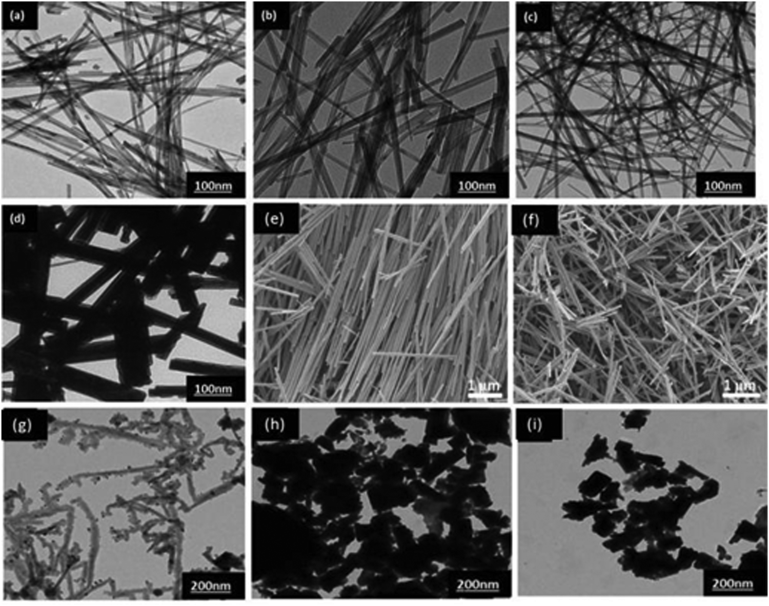 | ||
| Fig. 11 TEM and SEM images of tungsten oxide nanoparticles: (a) WO3−x-NW, (b) WO3-NT, (c) h-WO3-NW, (d–f) h-WO3-NR, and (g) (NH4)2SO4, and (h) and (i) CA and OA without K2SO4, respectively. Reproduced with permission.152 Copyright@2020, Elsevier. | ||
Zheng and co-workers290 reported various morphologies of WO3, i.e., nanorods, nanofibers, and nanoflakes, by changing the surfactant and reaction conditions, as shown in Fig. 12a–d. The impact of crystallinity and morphologies on the EC properties was also investigated. Accordingly, nanorods were grown via seed-mediated growth on an FTO substrate at pH 2 via the hydrothermal process without any hard organic templates, followed by annealing (Fig. 12b). The nanofibers grew on FTO at pH 2.4 with the assistance of KCl as a capping agent, keeping the temperature 160 °C for 4 h (Fig. 12c). For the nanoflakes, the pH was 1.5 and NaCl is used as the capping agent at 180 °C for 40 min (Fig. 12d). The WO3 nanorods grown on FTO showed a high optical modulation of 64%, coloration efficiency of 61 cm2 C−1, and switch speeds of 5 s and 6 s as shown in Fig. 12e–h. It was reported that the highly ordered WO3 nanorods grown on an FTO seed layer showed the best EC performance among the morphologies. High-temperature annealing also affected the EC properties, given that the annealed WO3 nanorod sample possessed a low optical modulation due to its long hexagonal tunnel, but short response time due to its high crystallinity.
 | ||
| Fig. 12 SEM images of (a) porous WO3 nanofibers, (b) WNRs-1, (c) WO3 nanoflake arrays, (d) WNRs-2. (e) EC mechanism of the WNRs the interface reaction process of Li-ions and electrons between WO3 and the electrolyte and the diffusion process of Li-ions in the WO3 crystal lattice. Reproduced with permission.290 Copyright@2015, RSC. | ||
5. Strategies to improve EC properties
5.1. WO2.72 hybridized/mixed composites
It is believed that composite materials can aggregate and boost the performance of two/more ingredients. The mixing of two active materials with matching behavior can achieve a dominant interfacial area to a large extent. In nanoscale composites, the structural organization is advantageous because the physicochemical features arise from the confined interfaces. However, in arbitrary mixing, even the active components of material blends may be affected/detrimental due to the fact that their passageways are tortuous, and there may be some inactive sites. These composites may be more beneficial for the deliberate design of architectures from their mesoscale structure.291,292 The metal oxide nanocomposites with template mesoscale architectures have fast switching kinetics and long cycle life. In this case, it has been reported that two degenerate metal oxide nanocrystals may efficiently modulate the NIR spectral transmittance via electrochemical charging, and then discharging of free electrons, which are responsible for LSPR trigger absorption.40,293,294 Hence, it can be concluded that NIR spectral light is much more intense at shorter wavelengths (700–1300 nm), which can be ideal for composite nanocrystals with LSPR absorption, and thus beneficial for dynamic solar light.Polyoxometalate nanoclusters (POMs) denote a familiar class of metal oxide cluster compounds with framework topologies, which possess electronic and optical properties.295,296 POMs as an electron reservoir undergo reversible multi-electron transfer reactions and significantly impart EC properties. Gu et al.122 studied the EC performance of crown-type polyoxometalates, K28Li5H7P8W48O184·92H2O (P8W48), and W18O49 nanowires coated on ITO glass via the LbL process, as shown in Fig. 13. The P8W48 anion is a visible light absorption material owing to its wide range of stability. In the reduced state, it may exhibit good absorptivity of visible light, while the W18O49 NWs are a candidate with excellent absorptivity of NIR light. The effects of the W18O49 NWs and P8W48 on near-infrared and visible-light selective modulation were studied via the self-assembly technique. Meanwhile, the W18O49 NWs or P8W48 anion are negatively charged species, which hybridized with the positively charged poly(ethylenimine) (PEI) polymer to create electrostatic interactions for alternating layer deposition of a multilayered film (abbreviated as (PEI/W18O49)n or (PEI/P8W48)n). The ITO glass was first activated via the LbL deposition of a polyelectrolyte multilayer of poly(sodium 4-styrene-sulfonate) (PSS) and PEI to increase the surface charges and surface affinity before the deposition of the (PEI/W18O49)n or (PEI/P8W48)n composite multilayer thin film. Due to the excellent stability of the films prepared using P8W48 and W18O49 and their precise structural control, the nanocomposites film achieved the high coloration efficiency of 42.31 cm2 C−1 at 500 nm and 287.49 cm2 C−1 at 1060 nm (Fig. 13e–h). The switching speeds for the transparent, NIR-blocking and broadband-blocking were 86 s, 52 s, and 26 s, respectively. The electrochemical cycle stability of the composite film after 500 cycles at wavelengths of 1060 nm and 500 nm was only 3.20% and 2.40%, respectively. The obtained results provide an effective way for the formation of composite-based functional smart glass.
 | ||
| Fig. 13 Transmittance spectra of [PSS(PEI/PSS)3(PEI/W18O49)30/(PEI/P8W48)20] film at different potentials, held for 4 min. (b) Relative transmittance change for [PSS(PEI/PSS)3(PEI/W18O49)30/(PEI/P8W48)20] film under different applied potentials; blue curve: NIR + Vis region, red curve: NIR region, and black curve: visible region, and digital photographs of the film at 0.4 V, −0.6 V, and −1.0 V, respectively. (c and d) In situ optical response of [PSS(PEI/PSS)3(PEI/W18O49)30/(PEI/P8W48)20] multilayer when switching between −0.60 V (100 s) and −1.0 V (100 s) to 0.4 V (200 s), where each step is measured at 1060 nm (c) and 500 nm (d). (e and f) Optical density variation as a function of charge density at 1060 nm (red curve) and 500 nm (black curve). The applied potential is −0.6 V (e) and −1.0 V (f) for 100 s. Corresponding schematic (i) shows the dual-band optical modulation. Reproduced with permission.122 Copyright@2018, ACS. | ||
Liu et al.257 and Wang et al.119 demonstrated that ITO-based coating films are hard, which can be damaged and lose conductivity after a certain degree of bending of the device structures. They used Ag nanowires as a conductive substrate support and deposited W18O49 nanowires for EC device applications. The Ag nanowires and W18O49 nanowires were orderly assembled via the Langmuir–Blodgett (LB) method257 to develop several layers with elevated conductivity and transmittance. The Ag–W18O49 nanowire co-assembled thin film obtained via the LB method was continuously transferred to a PET substrate as an EC smart cell electrode, as demonstrated in Fig. 14. An increase in the number of layers of W18O49 nanowires significantly increased the coloration efficiency, cyclic stability, and transmissivity, as shown in Fig. 14b, c, f and g. The Ag–W18O49 co-assembled nanowire film could bend to a very small radius of 1.2 cm without any mechanical loss, which showed an excellent EC performance and mechanical stability (1000 cycles), as shown in Fig. 14d and e.
 | ||
| Fig. 14 (a) Schematic of the fabrication of a flexible device. (b and c) Images of Ag–W18O49 nanowires. (d–f) Coloration and bleaching of Ag–W18O49 nanowires film before and after an applied potential. Reproduced with permission.119 Copyright@2017, ACS. | ||
An Ag–W18O49 co-assembled film was used to develop a multilayered nanowire network on an ITO-PET film over a large-area conductive substrate with tunable conductivity (7–40 Ω sq−1) and transmissivity (58–86% at 550 nm), as shown in Fig. 15a–e.119 The Ag–W18O49–LiClO4/PMMA/PC-ITO-PET hybrid all-in-one solid-state portable and flexible EC device is shown in the colored and bleached states, which could be bent to a radius of about 1.2 cm with 90% resistance retention (ΔR/R ≈ 8.3%) after more than 1000 cycles. Heo et al.123 produced a low-temperature mesoporous WO2.72–NbOx composite thin film on an ITO-PET supporting substrate, as shown in Fig. 16. Consequently, they realized a random/disordered arrangement of nanocrystal structures in organic media, which giving the opportunity to develop mesoporosity and overcoming the compact structure formulations (Fig. 16E and F). Ligand-stabilized WO2.72 nanorods were synthesized using W(CO)6 and Me3NO dissolved in oleylamine in a three-neck flask in an N2 glove box and annealing directly at 300 °C for 90 min. After the wet-chemical reaction, the colloidal solution was washed using isopropyl alcohol (IPA) and redispersed in toluene, which were repeated several times to produce clean high aspect ratio WO2.72 nanorods. They also synthesized low aspect ratio WO2.72 nanorods by reducing the Me3NO and oleylamine concentration, as shown in Fig. 16A. The obtained WO2.72 may contain highly encapsulated ligands, which were stripped using Meerwein's salts (Et3OBF4). Et3OBF4 was dissolved in acetonitrile (AN) and mixed with WO2.72 nanorods in toluene at a 1:1 ratio with constant stirring, centrifuged and then redispersed for repeated washing. Both the ligand-stripped and ligand-capped WO2.72 nanorods were spin-coated on clean ITO-PET substrates using different dispersion media to form thin films of about 300 nm. The results showed that ligand-stripped WO2.72 nanorods produced a thin mesoporous film due to the opposite electrostatic links, which prevented the spontaneous packing of the nanorods (Fig. 16E and F). After the fabrication of the WO2.72 nanorod thin film, a guest component solution composed of NbO2POM clusters and [N(CH3)4]6Nb10O28·6H2O was drop-casted on the fabricated film, and then immersed in a formic acid and absolute ethanol mixed solution and heated at 150 °C. The WOx–NbOx composite film fabricated on ITO-PET has the advantages of selective control of the Vis-NIR light transmission, fast switching, and long cycle life (Fig. 16G and H).
 | ||
| Fig. 15 (a) Schematic diagram of a solid EC device. Photographs showing the (b) bleached and (c) colored state of the EC devices in the bending state. The insets are photos without bending. (d) Photographs of the EC glasses model and (e) EC window model. Reproduced with permission.119 Copyright©2017, ACS. | ||
 | ||
| Fig. 16 (A and B) Low and high aspect ratio WO2.72 nanorods (top) and (C and D) their XRD and UV-vis absorbance spectra, respectively. Low and high aspect ratio (E) WO2.72 mesoporous film and (F) Nb-POM in-filled WO2.72 film (top). (G) Transmittance of composite film at various applied potentials and their corresponding photographs. (H) Charging and discharging profile at various potentials. Reproduced with permission.123 Copyright©2017, ACS. | ||
Kim et al.41 designed WO3−x nanocrystals and an amorphous niobium oxide nanocomposite mesoporous film. The obtained WO3−x–NbOx composite exhibited high charge–discharge kinetics and stability for about 2000 cycles. However, wet-synthesis of WO3−x nanocrystals via the direct heating of a mixture of tungsten salts without applied pressure requires harsh conditions, high temperature, and the product yield is small. Vuong et al.297 also employed similar procedures and reported the fabrication of a porous core–shell TiO2–WO3 nanowire structure film via sputter deposition using carbon nanotubes as a substrate and frequent thermal treatment. The particle size, morphology, electrochemical, and EC performance were studied and then compared with that of thin TiO2–WO3 composite films and single WO3 and TiO2 nanowires. The porous composite nanowires exhibited high proton intercalation capability with good reversible electrochemical cycles through intercalation and de-intercalation of the charge-compensating ions. Dulgerbaki and co-workers298 fabricated WO3/PEDOT hybrid films and Li co-workers299 fabricated W0.71Mo0.29O3/PEDOT:PSS hybrid film-modified electrodes, which exhibited highly improved EC performances, including fast switching kinetics, high coloration contrast, and tremendous coloration efficiency of >100 cm2 C−1 compared with the pure WO3 films.
5.2. WO3−x/metal/WO3/other EC bilayer architecture films
To strengthen the transparency and EC functionalities, soft coatings as dielectric/metal/dielectric (DMD) blends have been appealing in recent years as alternatives to ITO-coated substrates.300 Various dielectric materials, for example WO3, TiO2, MoO3, and ZnS, have been reported for the construction of DMD blends recently. The DMD assembly has also been extensively used in electrodes in organic optoelectronic devices, such as light-emitting diodes and organic solar cells.301–303 In DMD coatings, the WO3 film may perform a dual function, where it is anti-reflective for light in the transparent state and becomes absorbent in the colored state.293,304–307 Furthermore, DMD bilayer or trilayer films possess optimum resistivity (>15 Ω), high transparency (<80%) in the visible region, low thickness and superior flexibility.124,125,305–307 For dual functionality, the matrix design by simulation of D/M/WO3 as glass/ZnS (34 nm)/Ag (15 nm)/WO3 (326 nm) was formulated and verified v experiments by Leftheriotis’ team.304 The color coating simulation studies showed the asymmetry of the radiation propagation path, which is absorptive in one direction and highly reflective in the opposite direction. They also substituted the layer of ZnS with an optimum thickness of WO3 and the Ag layer with Au, and the addition of a 4th protective layer of Al2O3 demonstrated feasible replacements toward the optimum design. The film was produced via electron-beam gun deposition with a transparency of 57% and sheet conductivity of 9 Ω. The obtained results showed that the outer WO3 coating layer should be thick enough to protect the Ag nanolayer from the liquid electrolyte. The optical contrast was 90 cm2 C−1 and a coloration efficiency of 30 cm2 C−1 was recorded for 500 coloration/bleach cycles. The influence of liquid electrolyte on the EC coatings was observed with an increase in resistance and stability due to degradation, where the Ag nanolayer degraded because of the interactions of the electrolyte through the pores of the coated ZnS layers.308 Hence, a layer thickness of WO3 of up to 300 nm was adequate for the protection of the Ag nanolayer over the ZnS/Ag/ZnS stack.Koubli et al.306 employed electron beam deposition for the formation of a WO3/Ag/WO3 coating film. The fabricated film exhibited excellent deep coloration. However, with the intercalation of electrical charges, the film was unstable and damaged with the reversal of electrical potential. It became dysfunctional in the bleach state due to the reaction of Ag with Li+ ions, and the resistance of the Ag layer increased. Hence, for safe mode operation, the charge density was lowered to 12.6 mC cm−2 from 15.7 mC cm−2. Li et al.305 demonstrated that a WO3/Ag/WO3 film could sustain up to 3000 cycles without EC performance degradation, as shown in Fig. 17. The poor adhesion and rapid degradation regarding color/bleaching of the bifunctional WO3/Ag/WO3 film were improved by sputtering deposition using metal targets.125 They successfully added an ultrathin tungsten sacrificial layer followed by an external WO3 layer. Metal-to-metal bonds are generally stronger than metal-to-oxygen bonds. Therefore, the Ag-to-W layer film was adjusted to the desired thickness and the resulting film in the 2000th bleaching cycle showed a stable EC performance and avoided oxidation of the silver metal nanolayer in the oxygen atmosphere. Based on this strategy, the oxidation of silver metal (Ag0) can be eliminated and the conductivity of the film can be lost. Moreover, according to the conventional DMD three-layer structure, the introduction of a sacrificial W layer presents complexity to the deposition process in the form of a fourth structural layer in the device configuration.
 | ||
| Fig. 17 (a and b) Different layer thickness of WAW (30/10/50 nm) used as an electrode and their corresponding color and bleached states. (c) Transmittance variations with a change in voltage (0.6 to −0.6 V). (d) Current and optical contrast with step potential. (e) CV curves and (f) transmittance variations with different cycles. Reproduced with permission.305 Copyright@2015, Elsevier. | ||
Najafi-Ashtiani et al.309 used high-power impulse magnetron sputtering (HiPIMS) instead of DC/RF magnetron sputtering technology to produce aa DMD film without a fourth sacrificial metal layer, as illustrated in Fig. 18. The HiPIMS EC deposition method has a wide range of use in industry and production. Converting a traditional sputtering system to HiPIMS operation only requires the application of a suitable power supply to derive the target in the HiPIMS mode.310 The high instantaneous power supply produces high-density plasma of the sputtered target material with a high ionization degree.310 The limited supply of oxygen is promising for the controllable growth of WO3 nanoparticles and external layer deposition to reduce the oxidation of the Ag layer.309 The thickness of WO3 (30 nm)/Ag(10 nm)/WO3 (50 nm) was optimized with the sheet resistance of ∼23 Ω and transmittance of 80% (Fig. 18a). The fabricated coating exhibited an EC performance with good transparency, excellent cycling stability for 2500 cycles, fast switching kinetics, and Vis-NIR light modulation (Fig. 18b).
 | ||
| Fig. 18 HiPIMS-sputtered EC WO3/Ag/WO3 (DMD) three-layer structure. (a) WO3 deposited on ITO–FTO-coated glass. (b) Transparent, conductive DMD structure deposited on glass without ITO/FTO with a tungsten (W)-protective layer on the Ag layer. (c) DMD structure (ITO–FTO free) fabricated via HiPIMS without a protective layer. Optical images of bleached and colored states of the DMD (30 nm/10 nm/50 nm) coating. Reproduced with permission.309 Copyright@2019, ACS. | ||
The EC performance of DMD films is not satisfactory in terms of switching time, switching speed, optical modulation, and durability. To this end, the pioneering work of Dong et al.124 proved the application of mixed oxides of W–Mo-encapsulated Ag such as an MoO3–WO3/Ag/MoO3–WO3 trilayer film for ITO-free EC devices, as demonstrated in Fig. 19. The film thickness was optimized at 40 nm, resulting in the sheet resistance of 9 Ω with a fast-switching speed and high coloration efficiency (70 cm2 C−1).
 | ||
| Fig. 19 Optical transmittance of MAM, MWAMW, and WAW films in (a) colored and (b) bleached states at potential steps from −0.50 to 0.55 V (vs Ag/AgCl) with a 20 s interval. (c) Pictures of MAM, MWAMW and WAW films in the colored and bleached states. (d) Schematic of MWAMW composite deposited on PET or glass and corresponding color and bleached state optical transmittance. Reproduced with permission.124 Copyright@2016, ACS. | ||
5.3. Doped WO2.72 nanostructures
Using dopants or intended impurities to switch the behavior of nanomaterials is at the heart of various key technologies. For semiconductors, the doping process is crucial, otherwise they would be electrically insulating. Certain applications such as wavelength-tunable lasers,311 bioimaging,312 photocatalysis, and solar cells313 may eventually rely on the doping of nanocrystals to tune their electrical properties. Doping is an effective method to tailor the bandgap of semiconductor materials by introducing a transition state (defect band) between their valence bands and the conducting bands. Moreover, dopants can strongly alter the electronic, optical, and magnetic properties of bulk semiconductors.314 The EC efficiency of WO3−x/WO3 has been tested by doping315 with Mo, Nb, Ti, Ni, Al, Ag, Pd, Cu, Au, etc. The use of impurity atoms to tune the conductivity of WO3−x can be better understood by considering (i) substitutional doping and (ii) interstitial doping.Mo, Cu, and Nb are considered effective sensitizers, increasing the oxygen vacancies and crystal defects. Thus, the absorption peak position of the films shifts to a low wavelength range (blue shift). Moreover, they can also accelerate the reversible switching kinetics of the film.12,324 Al ion doping also adds advantages based on the shape, size, and structural variations.325 Li and Ru doping successfully enhanced the electrochemical performance, cycle stability, and diffusion coefficient of WO3-based thin films.77,326 As the size of nanocrystals decreases, their energy increases, and thus the carriers in the nanocrystals must occupy any confined electronic states.327 For robust/stable conductivity, adjacent nanocrystals should be uniform in size to have resonant electron states, and eventually, be narrowly spaced to confirm their quantum-mechanical overlap. Yao et al.328 synthesized Cr-doped WO3 polyhedra by controlling the parameters of RF thermal plasma. The results demonstrated that the 2.5 at% Cr-doped-layer could reduce the crystal growth rate of WO3 along the 〈001〉, 〈010〉, and 〈100〉 planes.
Higher carrier concentrations are required for superior conductivity. However, nanocrystals with additional free electrons and holes can also be used as strong reducing/oxidizing agents. Therefore, the electrochemical reactions on the surface can consume the charge carriers,329 and the carriers will not participate in electrochemical reactions. Thus, avoiding these reactions of films fabricated using doped nanocrystals is a big challenge! The n-type and p-type doping of CdSe quantum dots using In, Sn, Al, or Ag as dopants have been a research focus, as illustrated in Fig. 20a and b.330,331 The critical temperature affecting the doping processes can be summarized as follows:332 (i) surface adsorption, (ii) lattice incorporation, (iii) lattice diffusion, and (iv) lattice ejection (Fig. 20a and b). It is noteworthy that each nanocrystal can be switched, but it may be impossible to dope to achieve the desired doping characteristics.
 | ||
| Fig. 20 (a) Temperature-dependent surface adsorption, lattice incorporation, lattice diffusion, and lattice ejection doping in nanocrystals.332 (b) Mn2+ diffusion doping of CdSe nanocrystals and Mn2+ expulsion from Cd1–xMnxSe nanocrystals via cation exchange with Cd2+.332 Reproduced with permission. Copyright©JACS. | ||
To improve the energy saving proficiencies of EC smart windows, it is necessary to maximize the plasma resonance displacement and modulations of NIR rays. For example, in ITO, a high doping concentration shifts its LSPR peak to the high frequency spectrum. In contrast, a decrease in the nanocrystal size to ∼2–5 nm in accordance with an increase in optical modulation remains enigmatic. Smaller nanocrystals have a higher surface charge density, which facilitates high capacitive behavior and allows more electrons to be injected. Therefore, smaller size and highly doped nanocrystals will exhibit improved EC performances in the desired multifunctional EC smart windows. Because of the impurity atom doping and higher formation energy of defective nanocrystals, nanocrystals tend to expel dopants during annealing to minimize their energy and undergo self-purification/healing (Fig. 20).339 It was found that surface adsorption and diffusion339 can be influenced by three main factors: (i) surface morphology, (ii) nanocrystal shape, and (iii) surfactants in the growth solution. Based on the kinetic control, dopants can be incorporated in the host nanocrystals if they can bind and reside on the host crystal surface. Diffusion of impurities into the host nanocrystals may occur on the surface of nanocrystals. It was also found that nanocrystals contain active surface sites and the binding energy of the impurities adsorbed on the nanocrystals determine their residence time.339 The diffusion doping strategy is based on incorporating relatively incompatible anions/cations in semiconductors, which is driven by thermodynamic and high-temperature cation randomization. For, example Cd1−xMnxSe has been studied (Fig. 20b).340 The slow diffusion kinetics of Mn2+ ions and high-temperature treatment possibly accelerate their diffusion, although it is associated with self-purification due to the diffusion of Mn2+ ions out from the nanocrystals.332
It is worth noting that only effective doping that successfully incorporates dopants in the host crystal lattice rather than adsorbed on its surface can alter the characteristics properties of nanocrystals; however, plasmonic nanocrystals are quite interesting in this regard.314,340 Au and Ag are believed to have strong surface-enhanced Raman spectroscopy (SERS) performance. They have no signals upon Raman scattering but can produce strong LSPR under irradiation of light. Because Au couples with Ag substrates, and then non-noble metals, metal oxides, graphene, silicon-metal and metal-tellurides are also considered to become a new type of SERS materials due to the charge transfer mechanism. Liu and coworkers341 reported that TiO2 and WO3−x do not have free electrons because of their wide bandgaps, indicating that these semiconductors will not show the LSPR effect. However, their conductivity can be greatly enhanced due to the introduction of dopants into their large vacancy/defect sites, given that the dopant materials have the LSPR effect due to the free electrons found in their d-orbital, as shown in Fig. 4b and 21. However, the SERS induced due to the LSPR in TiO2−x and WO3−x cannot be generated due to the presence of oxygen vacancies and crystal defects. This can be attributed to the difference in excitation wavelength between NIR and SERS, which are found in the visible region. However, the conductivity (charge transfers) greatly increases due to the vacancy-doped features between the substrates and the adsorbed molecules. Therefore, if the LSPRs of vacancy-rich materials can be adjusted from the NIR region to the visible region (near the SERS excitation wavelength), then due to the charge transfer process, their SERS activity can be further improved. The high density and oriented W18O49 ultrafine nanowire bundles with an abundance of oxygen vacancies and defects have strong LSPR due to the charge transfer and electromagnetic enhancement factors. With an increase in thickness due to the aggregation of the nanowires, the absorption peaks gradually change from the NIR to visible region (Fig. 21). However, the XRD peaks remain almost the same, which was concluded to be due to electromagnetic oscillations found in the highly thin W18O49 nanowire bundles. These pioneering results may reveal SERS properties.341 The SERS enhancement mechanism can be attributed to the synergistic effect of the LSPR-SERS coupling that occurred among the ultrathin oriented nanowires, defects, and oxygen vacancy, which significantly improves the charge transfer process.341
 | ||
| Fig. 21 (a–c) TEM images of W18O49-561, W18O49-743, and W18O49-1025, distinguished due to various in their LSPR peaks. (d) HRTEM image of W18O49-561. (e) Cross-section of a 1.0 nm nanowire inside of one W18O49 unit cell oriented along the [010] direction. (f) UV-visible-NIR absorption spectra of the W18O49-561, W18O49-743, and W18O49-1025. (left) Top: Band structure of W18O49 and the two possible SERS enhancement ways in W18O49: (1) EM and (2) CT. Bottom: LSPR coupling between nanowires. Adopted from ref.341 Copyright©2018, ACS. | ||
5.4. Plasmonic surface-decorated WO2.72 composites
Plasmonic nanocrystal-modified interfaces significantly affect the optical absorption properties of nanomaterials. Noble metals nanocatalysts, such as Au, Pd, Pt, Ag, Rh, and Cu, are promising for improving the optical properties via LSPR effective modulations and Schottky junction formation. This is because the difference in the work functions of noble metals and the semiconductor metal oxide (WO2.72) induce electronic sensitization, affecting their electrical properties. The rectifying Schottky barrier at the interface enhances the electrical transport properties. Thus, a higher work function and Schottky junction formation can significantly facilitate the separation of photogenerated electrons and holes. Ordered-shaped plasmonic nanocrystals such as nanorods (1D), sheets (2D), cubes, and triangular prisms (3D) possess sharp edges and corners, and hence exhibit excellent LSPR and considerable electromagnetic field enhancement.Plasmonic-mediated nanocrystals can be classified into four categories as follows: (i) isotropic/bulk, (ii) assembled, (iii) responsive, and (iv) interfacial plasmonic nanocrystals. In bulk/isotropic plasmonic nanocrystals, the nanocrystal composite is monodispersed throughout the matrix compared to the bulk in a medium. The dielectric matrix may cause an insulating barrier between the plasmonic nanocrystal candidates or may also contribute to their optoelectronic properties. In assembled nanocrystals, the plasmonic component species are arranged into groups, clusters or certain anisotropic areas in the dielectric matrix. This self-assembly causes the nanoparticles to acquire strong plasmonic coupling due to the formation of nanojunctions and their collective optical properties. New research is devoted to reconfiguring the capability of plasmonic nanocrystals to modulate external stimuli that trigger a high optical response. Thus, the responsive plasmonic nanocrystals can acquire tunable and unique optical functionalities.10 It is noteworthy that the gaps between the nanocrystals often have an impact on their optical properties. The interfacial plasmonic nanocrystals connect the interfaces of the metal–dielectric (M–D), dielectric–dielectric (D–D) or dielectric–metal–dielectric (D–M–D). These composite architectures are frequently 2D/3D structures. Electron injection in 2D/3D plasmonic nanocrystal composites results in a shift towards the high-frequency region and optical modulation in the NIR region of the solar spectrum. Plasmonic composites are specially engineered to acquire optoelectronic properties different from their bulk components. The blend symmetries of plasmonic-incorporated particles can be understood based on Fig. 22, and detailed explanations can be found in the chemical review published by Su-Wen Hsu et al.342
 | ||
| Fig. 22 Schematic of the various classes of pNCs. Reproduced from ref. 342 Copyright@2018, ACS. | ||
The Vis-band optical modulation of WO3−x can be shifted towards the NIR wavelength due to the coupling of traditional metals/cation intercalation, resulting in NIR-LSPR extinction. Thus, the surface decorating/synthetic doping of noble metals in WO3−x nanocrystals should be capable of independent modulation of spectral bands in both the Vis and NIR regions within a single-component functionalized film. Thus functionalized WO3−x can be capable of dual-mode optical modulation as a nonradiative material to achieve multifunctional smart windows for controlling visible light transmittance, photothermal conversion of NIR solar loads, and also eliminating microorganisms living on windows.67,293,343,344 The growth of plasmonic nanocrystals on metal oxide layers can support the tunable LSPR, which will interact with the solar spectrum to shift the plasmon resonance for color changes.42 Moreover, Li-ion intercalated WO3−x can be used for energy storage applications, such as supercapacitors and batteries.133,345 Improving the slow diffusion kinetics of Li ions and the conductivity of bulk WO3−x can improve the charge capacity and charging capability of WO3−x-based electrodes. Assuming that surface-modified WO3−x can be charged, its charge capacity is almost equivalent to that of lithium insertion reactions in ultra-small particles of about 10 nm.42,346 Besides decreasing the size of WO3−x, doping can also improve the electrochemical properties of WO3−x electrodes (see Section 5.3) to boost their inherent low conductivity. Furthermore, surface-decorated nanocrystals with a diameter of <10 nm can support LSPR, which can be tuned through the Vis to NIR region by altering the size, shape, composition, and Fermi energy level of the nanocrystals, as reported in the literature.67,347,348 Au, Ag, and Pd nanoparticles may exhibit a strong, robust, stable, and tunable LSPR absorption band at both visible and NIR absorption wavelengths.69,349 Au and Pd nanoparticles with a spherical shape and size of ∼4–6 nm were deposited on the surface active sites of WO3 nanowire bundles in HAuCl4 and PdCl2 solutions with additional oxidation67,149,350 (Fig. 23). In this scenario, the absorbed NIR light could subsequently be converted to heat energy due to the electron–phonon/phonon–phonon interactions. Au NP-decorated WO3 may enhance the catalytic and photocatalytic activity and exploit the LSPR in Au NPs. The extensive work functions of Φ(Au) = 5.1 eV, Φ(Pd) = 5.5 eV, and Φ(WO3) = 4.8 eV may induce electronic sensitization and trap photo-excited electrons. The LSPR in gold-decorated WO3−x has been applied in photothermal ablation therapy,351 biological sensors,352,353 gas sensors,354–356 and optical detection.357
 | ||
| Fig. 23 (a–d) TEM and HRTEM images displaying WO3−x nanorods: nanowire assembly decorated with Au (a and b), Pd (c), and (d) bimetal Au, Pd NP-decorated WO3. (e and f) Corresponding EDS elemental mapping. Reproduced with permission.149 Copyright©Elsevier. | ||
Xu et al.293 fabricated an EC-photothermal dual-band composite film of plasmonic Au anchored with 3D honeycomb-like WO3, as shown in Fig. 24a–d. The obtained composite film was tested for the optical transmission and photothermal conversion of visible and NIR light and reducing the attack of microorganisms (Fig. 24e). The Au LSPR and broadband nonradiative plasmon decay are assumed to be tunable as an electric field on the surface of the WO3 substrate. The photothermal conversion was attained in a colored state, which is ascribed to the coupling of traditional visible-band optical switching with the NIR-LSPR extinction, as given in Fig. 24f and g. The as-prepared EC and photothermal films were also examined and proven to be effective in reducing the risk of microorganisms such as E. coli bacteria. Therefore, photothermal EC film-coated glass as an advanced multi-functional smart sterile window has broad application prospects.
 | ||
| Fig. 24 SEM images (a) top view and (b) magnified view of a blank WO3 film; (c) top view of Au nanoparticle-decorated WO3 film; and (d) top view of Au nanoparticle- and nanorod-decorated WO3 film. (e) Schematic of Au nanoparticle-attached nanorods, and digital photographs of the AuPR/WO3 film on FTO in the bleached and colored state. (f) Transmission spectra of the WO3, AuP/WO3, and AuPR/WO3 film-coated FTO slides at OCP and colored states. (g) Relationship of transmittance at 915 nm with an applied electrochemical potential at a scan rate of 10 mV s−1. Reproduced with permission from ref. 293 Copyright@2018, ACS. | ||
Moreover, Ag nanoparticles were distributed isotropically within the bulk polytetrafluoroethylene (PTFE) matrix through direct current (DC) or co-sputtering of Ag and PTFE to leverage the LSPR extension of the Ag nanoparticles in the visible range.342,358 The deposition process is important for developing flexible substrates that utilize matrix/nano-inks and target nanoparticles with a very small size. The plasmonic nanoparticle-based composite-generated film on the flexible substrates not only selectively controls the solar spectrum as an EC device but also has retrofit installation features.359 During in situ synthesis, the small size and morphology, and aspect ratio of plasmonic nanoparticles can cause impediments. Accordingly, plasmonic nanoparticle-polymer blends can successfully overcome this disadvantage via the incorporation of a polymer matrix in the already produced metal nanoparticles. Therefore, each material component of the plasmonic nanocrystals/composite can be synthesized independently and combined with the prospective polymer blend to generate a multifunctional nanocomposite.360–362
Nanoscale WO3−x particle decoration is advantageous for the fabrication of plasmonic nanocrystal-composites, which prevents undesirable aggregation or may be beneficial for phase separation. Similar to NiO, WO3, TiO2, and VO2, the color and optical transmittance can be tailored by external stimuli, including an electrical field, light, and temperature.10 In these scenarios, the nanocrystal components are grafted with polymer templates, which are miscible in a polymer matrix, i.e., dispersion of fullerenes in polystyrene.363 Similarly, they can also be grafted through the large gyration radius of linear polymers, i.e., polyethylene nanoparticles in polystyrene,363 and/or tethered with soft/hard templates having a high surface area, which endows the highest possible stability to the nanocrystal composite-polymer templates.364 Au nanorods were grafted with polystyrene polymer, and then deposited as a thin film.365 The thin film showed an optical response at 780 nm, which is reliable with the excitation of the longitudinal dipolar LSPR modes. The LSPR resonance function showed a blue shift in the optical absorption, resulting from the long linear-polymer templates and the side-by-side assembly of the aligned nanorods. In addition, the plasmonic EC film-based electrodes with nanocrystals in a disordered packing123 generated open network channels, which increased the surface area and could be easily accessed by the electrolyte. In this area of research, the Milliron team demonstrated the fabrication of porous films and the effect of the nanopore sizes obtained by using amphiphilic block copolymer micelles to bind ligand-stripped ITO nanocrystal architectures into an ordered/more alignment conductive mesoporous network.366 The mesoporosity was controlled by altering the molecular weights of the hydrophilic/hydrophobic block polymers, with the pore size in the range of 29–37 nm and thicknesses of 9–13 nm.366 The ordered mesoporous structures resulted from the interaction between the ligand-stripped nanostructure surface and hydrophilic block-copolymers.367 Increasing porosity increases the speed of ion transport and switching through the surface of the nanocrystals.347,367
In addition, the controllable size, quality, and assembly structure of plasmonic nanocomposites can be integrated into traditional multi-functional smart windows, where each component can be activated independently for specific functions. The independent modulation of visible and NIR light will stimulate the window to function in hot/cold climates to respond perfectly to changes in weather conditions. Recent research relies on plasmonic nanocomposite architectures for visible and NIR-selective transmission, enabling dual-band functionality to meet the challenges of traditional smart windows.122,123 Dahlman et al.42 fabricated a single-component colloidal aliovalent niobium-doped anatase TiO2 nanocrystal film for dual-band optical modulation. The Nb–TiO2-deposited film showed LSPR in the NIR region and could modulate light with capacitive charging. A variation in the composition, size, shape, and doping in the TiO2 nanocrystals greatly affected the efficiency of the EC film. The anatase TiO2 has low electrical conductivity and slow ion diffusion, which was improved by composite formation and impurity doping.
Moreover, multifunctional integrated devices have received tremendous research interest due to their low cost, lightweight, flexibility, and for monitoring health and the environment. Recent research achievements such as gas sensors, strain sensors, and photodetectors have been reported in various self-powered multifunctional integrated systems, thus reducing energy cost by cooling, heating, and lighting.68,293,368 For example, flexible supercapacitors have been reported together with photodetectors based on CdSe nanowires,369 Co2O3 nanowires on Ni fibers with graphene,370 TiO2 nanoparticles,371 and TiO2/MXene heterostructures372 deposited on different substrates. The resultant flexible all-solid-state integrated systems exhibit energy-storage performances together with an excellent response to white light. Yun et al.373 fabricated a stretchable SiC gas sensor for NO2 on an Ecoflex substrate, which could detect gas with a sensitivity of about 50 min after being charged. Moreover, flexible, self-powered devices have been reported, which are sensitive to human touch or motion.374 Kai et al.375 synthesized a stretchable conductive composite by mixing poly(3,4-ethylene dioxythiophene):p-toluene sulfonic acid (PEDOT:PTS) mixed with polyurethane (PU). The film fabricated by spin coating showed dynamic electrochromism in a hydrogel without supplying an external voltage, as given in Fig. 25. The stretchable PEDOT/PU film is suitable for a wearable display device; hence, it can be ultimate proof for the multifunctional features of wearable-to-self-powered with sensory smart window applications.
 | ||
| Fig. 25 Stretchable EC film of PEDOT/PU. (a) Molecular structures of PEDOT and photographs of the stretched EC film of a PEDOT/PU composite in the reduced and oxidized states. (b) Schematic illustration of an EC film/hydrogel hybrid. (c) EC film/hydrogel hybrid wrapped around a glass rod and human finger. (d) Color change in the EC film/hydrogel hybrid device placed on a human finger. Reproduced with permission.375 Copyright@2017, ACS. | ||
6. State-of-the-art EC devices: principal factors and composition
6.1. Principle factors
In an exemplary EC device (Fig. 1), cathode EC materials exhibit their inherent optical properties without an applied electrical potential, and the electrolyte ions (cations and anions) are uniformly dispersed in the device. When an electric potential is applied, the EC material captures the injected electrons, and thus the material gets reduced and then ionized, with a change in optical property to the “switching” mode. Meanwhile, the cations from the electrolyte move toward the opposite electrode and gather in the area of negatively ionized EC materials to balance the charge near the cathode. Also, the anions from the electrolyte enter the counter electrode to balance the charge and are stabilized by oxidization. Thus, fully reversible redox reactions occur with an appropriate reverse voltage. Therefore, the performance of EC devices depends not only on the electrochemical reaction of heterogeneous electron transfer between the electrode and the EC film and/or ion storage film, but also on the homogeneous ion(s) transfer through the EC layer(s), the ion-transport layer, and the ion-storage layer. Thus, the EC performance can be optimized as follows: (i) by increasing the surface activity between electrodes and the EC film and/or ion storage film; (ii) increasing the electronic conductivity of electrodes and/or the ionic conductivity of electrolytes; and (iii) advancement to EC materials.The EC material films are the key components defining the EC device performance, where the reversible optical modulation occurs under a suitable voltage. The dynamic windows consisting of WO3−x can be electrochemically/electronically color/bleached with the insertion of a tiny electric potential (1–3 V) to dynamically control the inlet/exit of thermal loads and daylight via smart windows of buildings, vehicles, aircraft, etc.
EC devices can be (i) single EC and (ii) dual/multiple EC.
(i) Single EC devices are developed from one EC material coated as a thin layer. This type comprises materials with alternative one coloured state and one bleached state, which is useful in absorption/transmission-type devices. These devices may have fewer redox states compared to that composed of more than one EC active species.
(ii) Dual/multiple EC devices consist of two/more active EC materials triggered for multifunctional features in a single platform (Fig. 1). However, two/more active materials on the same platform can cause system complexity. Nevertheless, they have significant advantages in the possibility of multiple color changes at small applied potentials and multifunction. Dual-function devices designed with cathode and anode EC materials in one platform (Fig. 1) are considered to be more efficient, powerful, and therefore can save a tremendous amount of energy.
Based on their operation, EC devices can be transmissive type, which operates on the principle of optical transmission, and reflective type, regulating the optical reflectance. Further progress remains to be achieved in developing more efficient multifunctional EC devices with different capabilities in a single platform. The key parameters used for evaluating the EC device performance are as follows:
6.1.1 Coloration efficiency
6.1.2 Switching time
6.1.3 Cycling life
6.1.4 Device stability and durability
| CE = ΔOD/Q = log[Tbleached(λ)/Tcolored(λ)]/Q | (7) |
6.2. Device configuration
Optical transparency and mechanical flexibility have become new developments in the next generation of flat panel electronics, enabling new technologies, including EC windows, (e)skin, wearable optoelectronics, and rolled-up displays.376,377 A traditional EC device is composed of a 4–5 layer configuration, and nanomaterials are widely used in each layer to achieve better performances and reliability. The recent advances on EC materials (inorganic/organic) have been reviewed by Yang et al.,84 Rai et al.,87 Kim and Yang,10 and Eh et al.,196 and the state-of-the-art approach of EC materials towards multifunctional EC smart-windows by Cai et al.83 and recent progress in smart windows based on electro-, thermo-, mechano-, and photochromics is summarized by Ke et al.8 The more recent development in EC materials triggered in each layer to build the next-generation smart windows for “zero-energy buildings” is summarized in this review, as illustrated in Fig. 26. | ||
| Fig. 26 Schematic illustration of the composition of EC devices. | ||
6.2.1 Transparent conductive substrates
6.2.2 Ion conducting electrolyte
6.2.3 Ion storage/conductive oxide counter electrodes (anode)
6.2.4 EC material (WO2.72) cathode
(i) Doped metal oxides. For EC glasses, thin transparent conducting films consisting of doped metal oxides are generally employed as conductive electrode supporting substrates. Common examples include In2O3:Sn (ITO), SnO2:F (FTO), SnO2:Sb (ATO), In2O3:Zn (IZO), ZnO:Al (AZO), ZnO:Si (SZO), ZnO:Ga (GZO), ZnO:B (BZO), ZnO:F (FZO), ZnO:Nb, ZnO:Sc, and SnO2:Ta.5,379 All these co-doped oxides have wide bandgaps and are transparent in both the visible and NIR light spectrum. They can develop several bilayer architectures with a combined resistivity of about ∼1 × 10⁻⁴–10−3 Ω cm−1, expected thickness of up to ∼300 nm, and can be reduced to a certain adequate value with excellent durability. With the arrival of flat-panel display devices, ITO became the most commonly used transparent conductive oxide material for transparent electrodes;378,379 however, it is still not available on a large scale for EC smart windows. All these oxides are transparent in the solar spectrum.
The large-scale integration of traditional wearable electrochromic devices requires the development of flexible, stretchable, and deformable substrates.196,372,375,377,380 Generally, polymer, CNTs, graphene, MXenes, metal film, plastic, carbon fibre, silicone, hydrogels, and paper are used as supporting substrates due to their outstanding mechanical flexibility and physiochemical stability (resistivity, heat, good acid–base corrosion resistance, etc.).380 ITO is cost-expensive and brittle. Thus, conductive coatings on the surface of flexible EC substrates may be destroyed and cracked due to excessive stretching and bending processes at a lower strain of 2–3%. Concerns have also been raised over the limited indium source, stringent deposition conditions, and consequently high costs.381 It is unstable in acidic/basic environments, which leads to a shortened device lifetime. Moreover, ITO films have a high refraction index, and thus can cause unwanted reflections.381
Polyethylene terephthalate (PET) supporting substrate is a commonly used bendable electrode material due to its easy manufacture, low cost, excellent flexibility, super transparency (>85%), and constancy in weak acids-bases.382,383 Thermal evaporation and photolithography can be applied for deposition on PET substrates; however, its brittleness and processing at high-temperature (150 °C) limit its use in flexible EC devices. Therefore, it is difficult to distribute the functional electrode materials and sensing materials on PET substrates through direct chemical preparation. ITO- and FTO-coated glass substrates have been replaced by PET/polymers (polyimide), and because of their excellent conductivity, these materials improve the cycle stability and colour efficiency, and hence are suitable for use in EC devices (Fig. 1).37 Polyimide (PI) sustains a high temperature (400 °C < 3%) without affecting wearability and transparency.380 Gas-phase and wet-chemical methods can be used to deposit materials on PI substrates, which demonstrates that the active materials have strong adhesion with the substrates, thereby improving their electrochemical properties. Moreover, ultra-thin silicon films (5–10 m) and mica plates are also a good choice for EC material growth and device manufacturing due to their high thermal stability (>600 °C). Graphite, carbon paper and MXenes have attracted great attention because of their foldable, bendable, and rollable properties. Flexible substrate-based electrodes in EC devices have retroflected installation ability on existing windows, which significantly reduces costs compared to new installations. However, for large-area practical applications, the development of flexible EC devices at present is in its infancy. For example, in advanced flexible EC devices, the effect of UV light on polyester/PET foils can cause degradation and will affect the lifetime of EC windows. To avoid the brittleness of FTO and ITO glass, some flexible transparent substrates such as graphene,384,385 carbon nanotubes (CNTs),386 metal nanowires,387,388 conducting polymers,302,303 and MXenes389 have been investigated as a substitute. However, the electrodes made up of these prevailing materials may suffer from limited transmittance in the bleached state.
(ii) Metal nanostructures. Metal grids and 1D noble metals nanoparticles such as Ag, Au, Cu, and Al have been tested as coatings for wearable substrates, which exhibit decent flexibility and excellent conductivity (Fig. 27).390 The metal-based coated layer should retain a low refractive index in the visible region and d-band contribution to the plasma wavelength oscillations in the UV range (∼320 nm). The d–d electronic transitions provide minimum reflectance of a shorter wavelength in the visible region closer to the plasma wavelength.300,391
 | ||
| Fig. 27 (right) SEM images of Ag NW films produced from Ag NWs with a diameter of 40–100 nm and different densities lead to different sheet resistances of: (a) 100, (b and c) 50, and (d) 15 Ω □−1. (f) 2.7 mg mL−1 Ag NW ink in ethanol solvent. (h) SEM image of Ag NW coating shown in panel c. The sheet resistance is ∼50 Ω □−1. (i) Optical transmittance of transparent Ag NW electrodes measured with a UV-vis spectrometer, without including the substrates. Reproduced with permission.387 Copyright©2010, ACS. (Left) (a) Schematic of the stretchable EC device. (b and c) Stretchable device is twisted and crumpled, showing excellent mechanical robustness. (d and e) Examples of the patterned device in the bleached and colored states at 0 and 50% strain, respectively. Reproduced with permission.392 Copyright©2014, ACS. | ||
Gold exhibits great potential because of its environmental stability and LSPR peaks that spectrally match with the solar emissions.293,393 Ag nanowire-based films are rapidly emerging due to their excellent conductivity, transparency, softness, and toughness, making them an auspicious candidate for the electrodes of next-generation wearable optoelectronics.84 The refractive index of silver is 0.06 and its extinction coefficient of 3.59 at λ = 550 nm is the most ideal choice among the noble and non-noble metals in recent research. It has limited absorption in the visible region with a neutral color and has excellent optoelectronic properties.300,394,395 Cu multi-layers films also increased in popularity and became the preferred choice for thin-coating technology because of their tunable performance and reduction in overall material size and cost.300 Metals nanowire-based electrodes have good connectivity, flexibility, and anti-deformation ability. However, they have certain limitations, where the nanowires have weak wire-to-wire interaction and poor adhesion with the substrates, making it easy for them to detach from the surface, thus shortening the coating lifetime. It is worth noting that pure metal nanowires are easily oxidized in air and have poor stability due to long-term electrochemical cycles. Therefore, new materials with ultrasmall size and excellent morphologies should be exploited to construct flexible substrates with lightweight, high electrochemical stability, high transparency, high interface adhesion of conductive layers, and high thermal management properties.
To improve the conductivity stability of silver-based transparent conductive electrodes, Cai's group83,114 and Li's group299 proposed replacing ITO with silver grids as flexible transparent conductive substrates, as shown in Fig. 28. A high conducting silver grid/PEDOT:PSS hybridized composite film with outstanding stability was developed. An ultrathin layer of WO3 nanoparticle coating was formed on an Ag-grid/PEDOT:PSS hybridized film, exhibiting the performance of flexible/foldable electrochromics. The hybrid-blend structure showed a large optical modulation of 81.9% at 633 nm, fast switching kinetics, and a high coloration efficiency of 124.5 cm2 C−1. Moreover, the hybrid film showed outstanding electrochemical cycling stability (sustaining 79.1% of its initial transmittance modulation after 1000 cycles) and remarkable mechanical flexibility (optical modulation decay of only 7.5% after 1200 compressive bending cycles). Consequently, a smart supercapacitor was developed as a conventional energy-storage device, which can simultaneously monitor the energy storage levels through rapid and reversible colour changes, even at high charge and discharge processes. The high-performance Ag-grid/PEDOT:PSS hybridized transparent films demonstrate a promising topology and a wide range of developing flexible electronics and photoelectronics. The high angle flexibility and bending nature of Ag nanowire-coated substrates maintain interconnectivity and can still illuminate light-emitting-diodes (LEDs) and bulbs after severe mechanical bending and deformation (Table 3).37
 | ||
| Fig. 28 Left (a) Schematic illustration of the structure of the silver grid/PEDOT:PSS hybrid film. (b) Transmittance spectra of WO3 in the colored (−0.7 V) and bleached (0.1 V) state over the wavelength range of 300–900 nm. (c–f) Transmittance and optical modulation changes of WO3 on the silver grid/PEDOT:PSS hybrid film in the bleached and colored state under repeated compressive bending (c and d) or tensile bending (e and f) with a curvature radius of 20 mm.114 Copyright@2016 Wiley-VCH. Right (a and b) FESEM images of the spray-LbL W0.71Mo0.29O3 electrode and (c and d) W0.71Mo0.29O3/PEDOT:PSS electrodes. (e) Schematic illustration and (f) optical transmittance. Reproduced with permission.299 Copyright©2018 ACS. | ||
| Electrode materials | Deposition method | Properties | Ref. |
|---|---|---|---|
| ITO thin film | Sputtering | R s = 10 Ω sq−1, T ≈ 90% | 396 |
| FTO thin film | Spray pyrolysis | R = ∼7 × 10⁻⁴ Ω cm; T = ∼90% | 397 |
| Ag NWs/PI | Wet process | R = 25 Ω sq−1, T = 86% | 398 |
| Ag NWs/PDMS | Spray process | R = 20 Ω sq−1, T = 75% | 399 |
| Ag NWs/PET | Lithographic filtration | — | 392 |
| Ag NWs/glass | Spin coating | R = 10 Ω sq−1, T = 60% | 85 |
| Ag NWs/PDMS | Spray coating | R = 20 Ω sq−1, T = 85% | 400 |
| Ag NWs/PMMA/glass | Spin coatings | R = 2 ± 0.1 Ω sq−1, T = 67% | 401 |
| Ag NWs/PDMS | Spray coating | R = 16 Ω sq−1, T = 87% | 402 |
| CNT/PDA nanofibers | Spinning coating | R = 100–1000 S cm−1 | 403 |
| CNT/PDMS | Paving method | R = 0.1–1 k S cm−1, T = 80% | 404 |
| Graphene/PET | Layer formation | R = 1∼2 kΩ sq−1, T = 97% | 405 |
| Graphene/PET-ITO | Electrodeposition | R = —, T = 80% | 406 |
| N-Graphene/glass | LPCVD | R = 1.1 kΩ sq−1, T = 93% | 407 |
| RGO/Cu NWs/glass | Spin coating/spray process | R = 34 ± 2.6 Ω sq−1, T = 80% | 408 |
| Ag NWs/PEDOT:PSS/PET | Spray process | R = 10 Ω sq−1, T = 86% | 409 |
| CNT/PANI/PET | Spray process | R = 364 Ω sq−1, T ≈ 94% | 410 |
| RGO/Ag NWs/Ag grid/PET | Bar rod coatings | R = 0.714 Ω sq−1, T = 90.9% | 411 |
(iii) Carbon nanotubes (CNTs). Due to their distinctive 1D nanostructure and unique mechanical and electrical properties, CNTs have achieved potential in many types of electronic devices. In particular, their inherent high conductivity, excellent flexibility, and stability, and relatively easy and low-cost preparation make them a promising electrode candidate for next-generation smart electronics. When CNTs act as electrodes for EC devices, they can also be employed as promising sensing elements and stretchable/flexible electronics for the prospective development of soft and versatile ends. Moreover, because of their compatible functionalized structure, they can also function as both an electrode candidate and EC smart material, which will further shorten the structure of EC devices and reduce their manufacturing costs.84
(iv) Graphene. The thinnest 2D carbon material has wide application prospects in many research fields because of its excellent electronic, optical, mechanical, and thermal properties.381 Graphene electrodes made of mechanically cracked graphene, CVD-grown graphene, or mass-produced graphene derivatives from bulk graphite have been used in a wide range of applications as an alternative to ITO transparent electrodes such as light emitting-diodes, touch screens, solar cells, field-effect transistors, batteries, supercapacitors, and sensors.381
(v) MXenes. Recently 2D transition metal carbides, nitrides, and carbonitrides known as MXenes have achieved wide research interest due to their flexibility, superior mechanical strength, physical/chemical properties, and multiplex tremendous functionalities.389 Because of their excellent electrochemical stabilities, mechanical properties, high ion adsorption capacities and charge transfer, metallic conductivities, and unique topology, MXenes have demonstrated innumerable potential applications in structural composites, electromagnetic interference (EMI) shielding materials, lithium-ion batteries (LIBs), supercapacitors (SCs), electrocatalysts, electronics, and topological insulators.256,389,412 Interestingly, 2D MXene nanosheets and their derivatives can be produced via wet-chemical synthesis, which makes it easy to self-assemble hybrid-films and unique structures.256,412,413 Thus, the effective combination of the mechanical and functional properties of MXenes emerges as a promising opportunity to design nanoscale flexible, foldable, and wearable EC devices on a large scale with superb durability.
Choi et al.428 deposited different size NiO particles on ITO glass through dry deposition, as shown in Fig. 29a–c. The electrochemical results showed that the nanoporous NiO film had a high charge storage capacity (49.49 mC cm−2) and lower charge transfer resistance (0.49 Ω). The porous structure and large active surface area enabled better contact with the electrolyte and ion diffusion in the nanoscale NiO fabricated film. The film showed an excellent transmittance modulation (42%), with a stable switching speed and electrochemical cycles. Kim et al.429 fabricated N-doped carbon-based porous NiO films via a sol–gel process with the assistance of oleylamine and amide condensation. The film showed the coloration efficiency of 48.5 cm2 C−1, color/bleach speed of 3.2/2.7 s, and specific capacitance of 235.8 F g−1 with the applied current density of 2 A g−1 (Fig. 29d–h). Wang et al.430 reported the electrochemical deposition of H3PW12O40 (PW12) on a TiO2 nanoparticle film coated on FTO glass, which functioned as an electron acceptor and redox shuttle for charge balancing of the TiO2 nanoparticles as the counter electrode (Fig. 29i–l). The hybrid film achieved 68% optical modulation at 1.5 V to −2.0 V applied voltage, cyclic stability (2500 cycles), and good coloration contrast.
 | ||
| Fig. 29 SEM image of NiO film. (b) Schematic illustration of the ion storage and charge capacity on ITO film. (c) Transmittance of the film as a counter electrode. Reproduced with permission.428 Copyright@2018, Elsevier. (d–g) FESEM images of N-doped carbon-based NiO in the presence of different amounts of oleylamine. (h) Schematic illustration of synthesis, followed by annealing. Reproduced with permission.429 Copyright@2021, Elsevier. (i) SEM images of TiO2 and (j) PW12–TiO2 film. (k) Transmittance of PW12–TiO2 at different voltages with photographs of the colored and bleach states. (l) Schematic of the various layers in the device. Reproduced with permission.430 Copyright@2019 WILEY-VCH. | ||
7. Challenges and perspective outlooks
7.1. Challenges
Chromogenic materials have been used for dynamic switchable smart windows; however, the commercialization of EC windows in the market is still hindered because of major problems including high manufacturing costs, material implementation, durability, and reliability. The significant challenges faced in the synthesis of WO3−x/WO3 nanostructures on a large scale and efficient film preparation are as follows:(i) Lack of standard synthetic methods for ultra-small size WO2.72/WO3 particles with a high surface area and EC electrode fabrication. It is very difficult to evaluate/compare the EC performance (coloration efficiency, switching speed, cycling life, cell stability, durability, etc.) reported in the literature.
(ii) Considering industrial applications, the synthesis methods are still far from market penetration due to the technical aspects and factors including quality, safety, cost, environmental hazard, mass production, and processability.
(iii) The phase-pure growth of WO2.72-based materials on the surface of electrodes with a controllable morphology and dimensions can achieve excellent EC performances due to fast electron/ion transportation, but this has been largely ignored. In the meantime, the loading (density/%) of WO2.72-based materials, electrode area, EC performance parameters, and other conditions should be stipulated.
(iv) The active WO2.72 nanostructure, plasmonic-doped or plasmonic-nanocomposite powders are considered ideal for practical applications due to the presence of conductive agents. However, smart techniques are required to overcome the inherent disadvantages and phase purity of each component.
(v) For generating multifunctionality, the shape, size and tunable porous film coatings of WO3−x-based plasmonic composites on wearable substrates acquire lightweight, high active surface area, and excellent conductivity. However, the charge/discharge capacity and expenses utilizing stretchable/deformable substrates are a key challenge for global researchers. Similarly, the optical modulation in white light and photothermal instability also need to be optimized.
(vi) When WO3/WO3−x tailored structures are deposited on a conductive substrate support, they can achieve relatively high electrochemical efficacy. However, at the device level, the cost may be quite high and the performance poor, with failure to reach the optical saturation threshold limit. Moreover, fast redox reactions/large electrochemical cycles result in EC dysfunction, and thus yellowing appears.
(vii) The mechanism through which oxygen vacancies/crystal defects and the electron/hole coupling in sub-stoichiometric WO3−x affect EC and electrochemical properties is not well understood experimentally and/or theoretically.
(viii) Self-chargeable, foldable/flexible smart windows with unique structural designs, non-sacrificing optical properties, and cost-effective materials are a growing future demand and can be implemented first in unique wearable applications, as part of energy storage systems.
7.2. Outlook
Due to their similarities with energy storage devices, e.g., supercapacitors and batteries, EC smart windows are known as transparent electrodes with reversible color states. Electrochromic supercapacitor devices (ESDs) with multicolor changes, energy harvesting and energy storage capacity, cyclic stability, and the realization of the quantitative monitoring of energy storage level of an ESD are very important to realize the practical application of the device.431,432 Conducting polymers have been studied as electrode materials for ESDs due to their rich color change and good energy storage performance.431 Pseudocapacitive materials simultaneously enable a high rate, high energy density, and energy storage systems based on ion intercalation.433,434 They can be incorporated into electrodes to minimize the mass-transfer limitations due to thickness effects, and electrolyte starvation/low particle-to-particle electron transport. For this purpose, WO3−x, NbOx, MoO2, and TiO2 with Mn, Ni, and Co oxides are appealing because of their properties related to storing electric charges and dynamic modulation of LSPR-absorption through capacitive charging/discharging.347 The 2D-layered materials known as MXenes have attracted much attention for applications in energy storage, optoelectronics, and photocatalysis.372 MXenes demonstrate excellent flexibility, are easy to process, with an ultrafine thickness of high conductivity, and possess the highest electromagnetic interference shielding effect. Thus, self-assembled MXene–WO3−x heterostructures should be employed as flexible and foldable energy storage EC films. The MXenes as a flexible transparent electrode and WO3−x as the flexible EC layer are expected to achieve excellent performances in flexible EC windows on a large scale. The charge-storage mechanism should be better understood based on pseudocapacitive/battery-type materials linked with WO2.72 to enrich the capacitive behavior for achieving self-powered multifunctionality. In addition, there is no clear quantitative relationship between the color change parameters and the energy storage level to achieve quantitative monitoring. This is because the constructed ESD is used to estimate the energy storage state through a color change. Under different charge–discharge voltages, the ESD displays different color.
Besides solar loads, human motions, and daily activities such as talking, walking, and running can produce a large amount of mechanical energy. Sensors that can harvest energy produced by human activities have been developed. Self-powered Wi-Fi-connected smart windows integrated with environmental sensors can read room occupancy and detect changes in the weather, gases, light, temperature, and mechanical deformations. These all-in-one self-driven, shape-adaptive versatile smart windows can be self-chargeable with solar energy/heat and gather energy by human interaction/motions, and various other types of sustainable mechanical energy conversion resources would be promising improvements.
In recent years, DMD (dielectric/metal/dielectric) blends have attracted increasing attention, in which the WO3 membrane can play a dual role of reflecting light energy in the bleaching state and absorbing in the colored state. In addition, Ag is an excellent heat-regulating material, which can also replace expensive substrates, e.g., FTO and ITO. The presence of extreme transmissive states in WO3−x/Ag/WO3−x allows the combination of numerous EC materials (hybrids) with controlled redox reactions to produce a variety of colors and bleach states with color coordination. In addition, the coloration efficiency and color coordination for WO2.72 electrochromism have not been investigated systematically, which complicates further advanced research. In the DMD architecture, the Cu and/or Al metals sandwiched between EC material layers are reliable and thermally reflective. Moreover, they can be promising in terms of cost, durability, and ease of processing. Researchers found that WO3, TiO2, SnO2, ZnO, CuS, ZnS, AlN, MoO2, and Nb2O5 can form functional multilayer structures that can functionalize conductive metals, for multi-coloration in EC smart windows.
Moreover, smart windows with unique novel multifunctional features extend their utility. Metal oxides become opaque upon ion extraction such as oxides of nickel and iridium or PEDOT/PSS materials. Among them, Ni is more functional, relatively common, and less expensive, which make it preferable for large-scale production. A device that can combine two types of EC functional materials, e.g., WO3−x and NiO, will be more advantageous, where the charges transfer from Ni to W oxide. In the opposite direction, the EC materials will be bleached (Fig. 1). It should be stated that the EC properties of NiO are different from that of WO3 in the case of Li+ ion-based electrolytes. The reason for this is that NiO involves surface sites for the exchange of both cations and anions.438 However, these novel multifunctional EC smart windows should be designed to enrich various EC materials coatings to convert solar loads into useful energy simultaneously,34 or to allow the transmission of visible light but reflect NIR light. Hybrid functional compatible electrochromics in a single platform are significant alternatives in balancing the performance limitations of one type of EC material by supplementing with the required activity of the competent material. Thus, enriching versatility in a smart way and minimizing the overall device size with superb service life will be fundamental approaches in the future.
The traditional vacuum evaporation, magnetron sputtering, and spin-coating methods are not suitable to achieve large-area coatings, controllable thickness, and low cost. Recently, our team has focused on different ways to produce ultra-thin films by rolling, spraying, casting/screen printing, and spin coating on various substrates, which shall remarkably reduce costs and readily achieve high-quality EC/TC smart responsive coatings to fulfill the huge market demands. However, the performance optimization and the commercial production still need more effort, as the researchers require cost-effectiveness, manufacturability, and market demand user willingness and policies. Thus, suitable and sustainable solutions to the problems addressed in this review regarding EC smart windows need to be found in the future.
Conflicts of interest
There are no conflicts to declare.Acknowledgements
This work was supported by the National Natural Science Foundation of China (21876062), and the Key R&D Program of Shandong Province (2019GSF109071). Thanks to the China Scholarship Council (2017DFH011650) for International Doctoral Students in China. This work was also fully sponsored by Shandong Shenna Smart Advanced Materials Co. Ltd.References
- C. G. Granqvist, in Handbook of Inorganic Electrochromic Materials, ed. C. G. Granqvist, Elsevier Science B.V., Amsterdam, 1995, pp. vii–viii DOI:10.1016/B978-044489930-9/50000-3.
- A. Pawlicka, C. O. Avellaneda, M. M. Silva and F. Kajzar, Nonlinear Opt., Quantum Opt., 2019, 50, 165–182 CAS.
- S. K. Deb, Philos. Mag., 1973, 27, 801–822 CrossRef CAS.
- S. K. Deb, Appl. Opt., 1969, 8, 192–195 CrossRef PubMed.
- C. Granqvist, Thin Solid Films, 2014, 564, 1–38 CrossRef CAS.
- J. S. E. M. Svensson and C. G. Granqvist, Sol. Energy Mater., 1984, 11, 29–34 CrossRef CAS.
- C. M. Lampert, Electrochromic materials and devices for energy-efficient windows, Lawrence Berkeley Lab., 1984 Search PubMed.
- Y. Ke, J. Chen, G. Lin, S. Wang, Y. Zhou, J. Yin, P. S. Lee and Y. Long, Adv. Energy Mater., 2019, 9, 1902066 CrossRef CAS.
- H. Khandelwal, A. P. H. J. Schenning and M. G. Debije, Adv. Energy Mater., 2017, 7, 1602209 CrossRef.
- H.-N. Kim and S. Yang, Adv. Funct. Mater., 2020, 30, 1902597 CrossRef CAS.
- C. Bechinger, S. Ferrere, A. Zaban, J. Sprague and B. A. Gregg, Nature, 1996, 383, 608–610 CrossRef CAS.
- S. Wang, W. Fan, Z. Liu, A. Yu and X. Jiang, J. Mater. Chem. C, 2018, 6, 191–212 RSC.
- Y. Wang, E. L. Runnerstrom and D. J. Milliron, Annu. Rev. Chem. Biomol. Eng., 2016, 7, 283–304 CrossRef CAS PubMed.
- A. Cannavale, P. Cossari, G. E. Eperon, S. Colella, F. Fiorito, G. Gigli, H. J. Snaith and A. Listorti, Energy Environ. Sci., 2016, 9, 2682–2719 RSC.
- Y. Ke, C. Zhou, Y. Zhou, S. Wang, S. H. Chan and Y. Long, Adv. Funct. Mater., 2018, 28, 1800113 CrossRef.
- L. Peng, B. Su, A. Yu and X. Jiang, Cellulose, 2019, 26, 6415–6448 CrossRef.
- X. Jiang, M. Soltani, E. Haddad, R. Kruzelecky, D. Nikanpour and M. Chaker, J. Spacecr. Rockets, 2006, 43, 497–500 CrossRef CAS.
- L. Peng, W. Fan, D. Li, S. Wang, Z. Liu, A. Yu and X. Jiang, Adv. Mater. Technol., 2020, 5, 1900599 CrossRef CAS.
- L. Liu, M. Liu, W. Fan, C. Zhao, X. Jiang, A. Yu and J. Wu, CN Pat., 109575713A, 2019 Search PubMed.
- M. Liu, B. Su, Y. V. Kaneti, Y. Tang, X. Jiang, A. Yu, Z. Chen, Y. Gao, Y. Yuan and L. Jiang, ACS Nano, 2017, 11, 407–415 CrossRef CAS PubMed.
- H. Zhu, Z. Zhang, M. Liu, W. Fan and X. Jiang, J. Nanosci. Nanotechnol., 2019, 19, 3597–3603 CrossRef CAS PubMed.
- H. Xu, Z. Dai, C. Wang, K. Xu, F. Ma and P. K. Chu, J. Mater. Chem. C, 2018, 6, 7896–7904 RSC.
- S. Wang, M. Liu, L. Kong, Y. Long, X. Jiang and A. Yu, Prog. Mater. Sci., 2016, 81, 1–54 CrossRef CAS.
- P. Castillero, V. Rico-Gavira, C. López-Santos, A. Barranco, V. Pérez-Dieste, C. Escudero, J. P. Espinós and A. R. González-Elipe, J. Phys. Chem. C, 2017, 121, 15719–15727 CrossRef CAS.
- O. F. Schirmer, V. Wittwer, G. Baur and G. Brandt, J. Electrochem. Soc., 1977, 124, 749–753 CrossRef CAS.
- R. Baetens, B. P. Jelle and A. Gustavsen, Sol. Energy Mater. Sol. Cells, 2010, 94, 87–105 CrossRef CAS.
- M. Tian and C. Shang, Int. J. Hydrogen Energy, 2019, 44, 338–344 CrossRef CAS.
- Y. Liu, J. Chen, L. Peng, N. Deng and W. Ding, Int. J. Hydrogen Energy, 2019, 44, 15205–15217 CrossRef CAS.
- Y. Liu, J. Chen, L. Peng, J. Han, N. Deng, W. Ding and W. Chen, Mater. Des., 2018, 144, 256–262 CrossRef CAS.
- J. S. E. M. Svensson and C. G. Granqvist, Thin Solid Films, 1985, 126, 31–36 CrossRef CAS.
- M. Antinucci, B. Chevalier and A. Ferriolo, Sol. Energy Mater. Sol. Cells, 1995, 39, 271–287 CrossRef CAS.
- M. Gratzel, Nature, 2001, 409, 575–576 CrossRef CAS PubMed.
- A. Llordes, G. Garcia, J. Gazquez and D. J. Milliron, Nature, 2013, 500, 323–326 CrossRef CAS PubMed.
- H. Chou, A. Nguyen, A. Chortos, J. W. F. To, C. Lu, J. Mei, T. Kurosawa, W. Bae, J. B. H. Tok and Z. Bao, Nat. Commun., 2015, 6, 8011 CrossRef CAS PubMed.
- G. Cai, J. Tu, C. Gu, J. Zhang, J. Chen, D. Zhou, S. J. Shi and X. Wang, J. Mater. Chem., 2013, 1, 4286–4292 RSC.
- G. Cai, J. Tu, J. Zhang, Y. J. Mai, Y. Lu, C. Gu and X. Wang, Nanoscale, 2012, 4, 5724–5730 RSC.
- G. Cai, J. Wang and P. S. Lee, Acc. Chem. Res., 2016, 49, 1469–1476 CrossRef CAS PubMed.
- W. Wu, M. Wang, J. Ma, Y. Cao and Y. Deng, Adv. Electron. Mater., 2018, 4, 1800185 CrossRef.
- C. L. Bird and A. T. Kuhn, Chem. Soc. Rev., 1981, 10, 49–82 RSC.
- G. Garcia, R. Buonsanti, A. Llordes, E. L. Runnerstrom, A. Bergerud and D. J. Milliron, Adv. Opt. Mater., 2013, 1, 215–220 CrossRef.
- J. Kim, G. K. Ong, Y. Wang, G. Leblanc, T. E. Williams, T. M. Mattox, B. A. Helms and D. J. Milliron, Nano Lett., 2015, 15, 5574–5579 CrossRef CAS PubMed.
- C. J. Dahlman, Y. Tan, M. A. Marcus and D. J. Milliron, J. Am. Chem. Soc., 2015, 137, 9160–9166 CrossRef CAS PubMed.
- M. Pugliese, F. Bisconti, A. Rizzo, S. Colella, C. T. Prontera, G. Gigli, V. Maiorano and P. Cossari, ACS Appl. Energy Mater., 2020, 3, 10453–10462 CrossRef CAS.
- C. J. Barile, D. J. Slotcavage and M. D. McGehee, Chem. Mater., 2016, 28, 1439–1445 CrossRef CAS.
- Y. Zhai, Y. Wang, X. Zhu, Z. Xing, S. Qi, S. Wang, Y. Han and Z. Chen, Macromolecules, 2021, 54, 5249–5259 CrossRef CAS.
- X. Lv, W. Li, M. Ouyang, Y. Zhang, D. S. Wright and C. Zhang, J. Mater. Chem. C, 2017, 5, 12–28 RSC.
- H.-J. Yen and G.-S. Liou, Prog. Polym. Sci., 2019, 89, 250–287 CrossRef CAS.
- C. K. Lo, D. E. Shen and J. R. Reynolds, Macromolecules, 2019, 52, 6773–6779 CrossRef CAS.
- H. Yu, S. Shao, L. Yan, H. Meng, Y. He, C. Yao, P. Xu, X. Zhang, W. Hu and W. Huang, J. Mater. Chem. C, 2016, 4, 2269–2273 RSC.
- C. N. Us and M. Icli Ozkut, Macromolecules, 2016, 49, 3009–3015 CrossRef CAS.
- H.-J. Yen and G.-S. Liou, Polym. Chem., 2018, 9, 3001–3018 RSC.
- S. Schraff, Y. Sun and F. Pammer, Macromolecules, 2018, 51, 5323–5335 CrossRef CAS.
- Y. Han, Z. Xing, P. Ma, S. Li, C. Wang, Z. Jiang and Z. Chen, ACS Appl. Mater. Interfaces, 2020, 12, 7529–7538 CrossRef CAS PubMed.
- Y. Han, Y. Lin, D. Sun, Z. Xing, Z. Jiang and Z. Chen, Dyes Pigm., 2019, 163, 40–47 CrossRef CAS.
- A. Chaudhary, D. K. Pathak, M. Tanwar, J. Koch, H. Pfnür and R. Kumar, J. Mater. Chem. C, 2020, 8, 1773–1780 RSC.
- H. Oh, J. K. Lee, Y. M. Kim, T. Y. Yun, U. Jeong and H. C. Moon, ACS Appl. Mater. Interfaces, 2019, 11, 45959–45968 CrossRef CAS PubMed.
- T. Y. Yun and H. C. Moon, Org. Electron., 2018, 56, 178–185 CrossRef CAS.
- Y. Alesanco, J. Palenzuela, A. Viñuales, G. Cabañero, H. J. Grande and I. Odriozola, ChemElectroChem, 2015, 2, 218–223 CrossRef CAS.
- J.-W. Kim and J.-M. Myoung, Adv. Funct. Mater., 2019, 29, 1808911 CrossRef.
- M. Kim, Y. M. Kim and H. C. Moon, RSC Adv., 2020, 10, 394–401 RSC.
- G. K. Pande, N. Kim, J. H. Choi, G. Balamurugan, H. C. Moon and J. S. Park, Sol. Energy Mater. Sol. Cells, 2019, 197, 25–31 CrossRef CAS.
- H. C. Moon, C.-H. Kim, T. P. Lodge and C. D. Frisbie, ACS Appl. Mater. Interfaces, 2016, 8, 6252–6260 CrossRef CAS PubMed.
- J.-W. Kim and J.-M. Myoung, Adv. Funct. Mater., 2019, 29, 1808911 CrossRef.
- Y. R. In, Y. M. Kim, Y. Lee, W. Y. Choi, S. H. Kim, S. W. Lee and H. C. Moon, ACS Appl. Mater. Interfaces, 2020, 12, 30635–30642 CrossRef CAS PubMed.
- R. J. Mortimer, A. L. Dyer and J. R. Reynolds, Displays, 2006, 27, 2–18 CrossRef CAS.
- J. Wang, L. Zhang, L. Yu, Z. Jiao, H. Xie, X. W. Lou and X. W. Sun, Nat. Commun., 2014, 5, 4921 CrossRef CAS PubMed.
- M. Guo, Q. Yu, X. Wang, W. Xu, Y. Wei, Y. Ma, J. Yu and B. Ding, ACS Appl. Mater. Interfaces, 2021, 13, 5634–5644 CrossRef CAS PubMed.
- S.-W. Oh, S.-M. Nam, S.-H. Kim, T.-H. Yoon and W. S. Kim, ACS Appl. Mater. Interfaces, 2021, 13, 5028–5033 CrossRef CAS PubMed.
- X. Li, W. Xie, C. Sui and P.-C. Hsu, ACS Materials Lett., 2020, 2, 1624–1643 CrossRef CAS.
- Y. Zhao, X. Zhang, X. Chen, W. Li, L. Wang, F. Ren, J. Zhao, F. Endres and Y. Li, ACS Sustainable Chem. Eng., 2020, 8, 11658–11666 CrossRef CAS.
- X. Huo, H. Zhang, W. Shen, X. Miao, M. Zhang and M. Guo, J. Mater. Chem. A, 2019, 7, 16867–16875 RSC.
- Y.-C. Her and C.-C. Chang, CrystEngComm, 2014, 16, 5379–5386 RSC.
- K.-W. Kim, Y. M. Kim, X. Li, T. Ha, S. H. Kim, H. C. Moon and S. W. Lee, Nanomaterials, 2020, 10, 821 CrossRef CAS PubMed.
- P.-W. Chen, C.-T. Chang, T.-F. Ko, S.-C. Hsu, K.-D. Li and J.-Y. Wu, Sci. Rep., 2020, 10, 8430 CrossRef CAS PubMed.
- E. A. Rojas-Gonzalez and G. A. Niklasson, arXiv.org, e-Print Arch., Phys., 2020, 1–10 Search PubMed.
- S. Mujawar, B. Dhale and P. S. Patil, Mater. Today: Proc., 2020, 23, 430–436 CAS.
- S. R. Bathe and P. S. Patil, Mater. Sci. Eng., B, 2020, 257, 114542 CrossRef CAS.
- E. Hopmann, B. N. Carnio, C. J. Firby, B. Y. Shahriar and A. Y. Elezzabi, Nano Lett., 2021, 21, 1955–1961 CrossRef CAS PubMed.
- D. T. Gillaspie, R. C. Tenent and A. C. Dillon, J. Mater. Chem., 2010, 20, 9585–9592 RSC.
- O. Lev, Z. Wu, S. Bharathi, V. Glezer, A. Modestov, J. Gun, L. Rabinovich and S. Sampath, Chem. Mater., 1997, 9, 2354–2375 CrossRef CAS.
- J. Yan, T. Wang, G. Wu, W. Dai, N. Guan, L. Li and J. Gong, Adv. Mater., 2015, 27, 1580–1586 CrossRef CAS PubMed.
- S. A. Agnihotry, Bull. Electrochem., 1996, 12, 707–712 CAS.
- G. Cai, A. L.-S. Eh, L. Ji and P. S. Lee, Adv. Sustainable Syst., 2017, 1, 1700074 CrossRef.
- G. Yang, Y.-M. Zhang, Y. Cai, B. Yang, C. Gu and S. X.-A. Zhang, Chem. Soc. Rev., 2020, 49, 8687–8720 RSC.
- K. Zhou, H. Wang, S. Zhang, J. Jiu, J. Liu, Y. Zhang and H. Yan, J. Mater. Sci., 2017, 52, 12783–12794 CrossRef CAS.
- G. Cai, M. Cui, V. Kumar, P. Darmawan, J. Wang, X. Wang, A. L. Eh, K. Qian and P. S. Lee, Chem. Sci., 2016, 7, 1373–1382 RSC.
- V. Rai, R. S. Singh, D. J. Blackwood and D. Zhili, Adv. Eng. Mater., 2020, 22, 2000082 CrossRef CAS.
- S. Cong, F. Geng and Z. Zhao, Adv. Mater., 2016, 28, 10518–10528 CrossRef CAS PubMed.
- W. He, Y. Liu, Z. Wan and C. Jia, RSC Adv., 2016, 6, 68997–69006 RSC.
- S. Bogati, A. Georg and W. Graf, Sol. Energy Mater. Sol. Cells, 2017, 159, 395–404 CrossRef CAS.
- K. S. Usha, R. Sivakumar, C. Sanjeeviraja, V. Sathe, V. Ganesan and T. Y. Wang, RSC Adv., 2016, 6, 79668–79680 RSC.
- M. Kateb, S. Safarian, M. Kolahdouz, M. Fathipour and V. Ahamdi, Sol. Energy Mater. Sol. Cells, 2016, 145, 200–205 CrossRef CAS.
- J. Zhang, Z. Chen, L. Yang, F. Hu, G. Yu, J. Yin and S. Liu, Dyes Pigm., 2017, 136, 168–174 CrossRef CAS.
- J. Zhang, G. Liu, X.-Y. Wang, G.-A. Yu, J. Yin and S.-H. Liu, Dyes Pigm., 2017, 143, 416–426 CrossRef CAS.
- B. Chiou, H. Lee, Y. Jang, Z. Yang, Y. Wang, M. Sarma, H. Su and K. Wong, Org. Electron., 2017, 48, 248–253 CrossRef CAS.
- W. Zhang, W. Ju, X. Wu, Y. Wang, Q. Wang, H. Zhou, S. Wang and C. Hu, Appl. Surf. Sci., 2016, 367, 542–551 CrossRef CAS.
- G. Nie, L. Wang and C. Liu, J. Mater. Chem. C, 2015, 3, 11318–11325 RSC.
- E. C. Cho, C. W. Changjian, Y. Hsiao, K. C. Lee and J. Huang, Sol. Energy Mater. Sol. Cells, 2016, 150, 43–50 CrossRef CAS.
- Y. Ji, C. Zhang, H. Niu, X. Zhao, C. Wang, C. Qin, W. Wang and X. Bai, Dyes Pigm., 2016, 125, 106–115 CrossRef CAS.
- N. Deforest, A. Shehabi, G. Garcia, J. B. Greenblatt, E. Masanet, E. S. Lee, S. Selkowitz and D. J. Milliron, Build. Environ., 2013, 61, 160–168 CrossRef.
- S.-H. Lee, R. Deshpande, P. A. Parilla, K. M. Jones, B. To, A. H. Mahan and A. C. Dillon, Adv. Mater., 2006, 18, 763–766 CrossRef CAS.
- P. Yang, P. Sun, Z. Chai, L. Huang, X. Cai, S. Tan, J. Song and W. Mai, Angew. Chem., 2014, 53, 11935–11939 CrossRef CAS PubMed.
- R. Wen, C. Granqvist and G. A. Niklasson, Nat. Mater., 2015, 14, 996–1001 CrossRef CAS PubMed.
- V. K. Thakur, G. Ding, J. Ma, P. S. Lee and X. Lu, Adv. Mater., 2012, 24, 4071–4096 CrossRef CAS PubMed.
- E. Hwang, S. Seo, S. Bak, H. Lee, M. Min and H. Lee, Adv. Mater., 2014, 26, 5129–5136 CrossRef CAS PubMed.
- A. A. Argun, P. Aubert, B. C. Thompson, I. Schwendeman, C. L. Gaupp, J. K. Hwang, N. J. Pinto, D. B. Tanner, A. G. Macdiarmid and J. R. Reynolds, Chem. Mater., 2004, 16, 4401–4412 CrossRef CAS.
- H. Wei, X. Yan, S. Wu, Z. Luo, S. Wei and Z. Guo, J. Phys. Chem. C, 2012, 116, 25052–25064 CrossRef CAS.
- M. Cui, W. S. Ng, X. Wang, P. Darmawan and P. S. Lee, Adv. Funct. Mater., 2015, 25, 401–408 CrossRef CAS.
- J. H. Jensen, M. Hosel, A. L. Dyer and F. C. Krebs, Adv. Funct. Mater., 2015, 25, 2073–2090 CrossRef CAS.
- P. M. Beaujuge and J. R. Reynolds, Chem. Rev., 2010, 110, 268–320 CrossRef CAS PubMed.
- J. He, L. You and J. Mei, ACS Appl. Mater. Interfaces, 2017, 9, 34122–34130 CrossRef CAS PubMed.
- H. Oh, D. G. Seo, T. Y. Yun, C. Y. Kim and H. C. Moon, ACS Appl. Mater. Interfaces, 2017, 9, 7658–7665 CrossRef CAS PubMed.
- X. Liu, L. Kong, H. Du, Y. Zhang, J. Zhao and Y. Xie, Org. Electron., 2019, 64, 223–235 CrossRef CAS.
- G. Cai, P. Darmawan, M. Cui, J. Wang, J. Chen, S. Magdassi and P. S. Lee, Adv. Eng. Mater., 2016, 6, 1501882 Search PubMed.
- C. Guillén and J. Herrero, J. Mater. Sci. Technol., 2021, 78, 223–228 CrossRef.
- H. Yu, J. Guo, C. Wang, J. Zhang, J. Liu, X. Zhong, G. Dong and X. Diao, Electrochim. Acta, 2019, 318, 644–650 CrossRef CAS.
- R. Baetens, B. P. Jelle and A. Gustavsen, Sol. Energy Mater. Sol. Cells, 2010, 94, 87–105 CrossRef CAS.
- T. V. Nguyen, K. A. Huynh, Q. V. Le, H. Kim, S. H. Ahn and S. Y. Kim, Int. J. Energy Res., 2021, 45, 8061–8072 CrossRef CAS.
- J. Wang, Y. Lu, H. Li, J. Liu and S. Yu, J. Am. Chem. Soc., 2017, 139, 9921–9926 CrossRef CAS PubMed.
- K.-W. Kim, T. Y. Yun, S.-H. You, X. Tang, J. Lee, Y. Seo, Y.-T. Kim, S. H. Kim, H. C. Moon and J. K. Kim, NPG Asia Mater., 2020, 12, 84 CrossRef CAS.
- Z. Wang, W. Gong, X. Wang, Z. Chen, X. Chen, J. Chen, H. Sun, G. Song, S. Cong, F. Geng and Z. Zhao, ACS Appl. Mater. Interfaces, 2020, 12, 33917–33925 CrossRef CAS PubMed.
- H. Gu, C. Guo, S. Zhang, L. Bi, T. Li, T. Sun and S. Liu, ACS Nano, 2018, 12, 559–567 CrossRef CAS PubMed.
- S. Heo, J. Kim, G. K. Ong and D. J. Milliron, Nano Lett., 2017, 17, 5756–5761 CrossRef CAS PubMed.
- W. Dong, Y. Lv, L. Xiao, Y. Fan, N. Zhang and X. Liu, ACS Appl. Mater. Interfaces, 2016, 8, 33842–33847 CrossRef CAS PubMed.
- Y. Yin, C. Lan, H. Guo and C. Li, ACS Appl. Mater. Interfaces, 2016, 8, 3861–3867 CrossRef CAS PubMed.
- J. Liu, O. Margeat, W. Dachraoui, X. Liu, M. Fahlman and J. Ackermann, Adv. Funct. Mater., 2014, 24, 6029–6037 CrossRef CAS.
- X. Dang, X. Jiang, T. Zhang and H. Zhao, Chin. J. Chem., 2021, 39, 1706–1715 CrossRef CAS.
- D. Chatzikyriakou, N. Krins, B. Gilbert, P. Colson, J. Dewalque, J. Denayer, R. Cloots and C. Henrist, Electrochim. Acta, 2014, 137, 75–82 CrossRef CAS.
- P. R. Bueno, R. C. Faria, C. O. Avellaneda, E. R. Leite and L. O. S. Bulhões, Solid State Ionics, 2003, 158, 415–426 CrossRef CAS.
- C. Bechinger, M. S. Burdis and J. Zhang, Solid State Commun., 1997, 101, 753–756 CrossRef CAS.
- S. Lee, H. M. Cheong, C. E. Tracy, A. Mascarenhas, A. W. Czanderna and S. K. Deb, Appl. Phys. Lett., 1999, 75, 1541–1543 CrossRef CAS.
- A. Al Mohammad and M. Gillet, Thin Solid Films, 2002, 408, 302–309 CrossRef CAS.
- P. A. Shinde and S. C. Jun, ChemSusChem, 2020, 13, 11–38 CrossRef CAS PubMed.
- Z. Shen, Z. Zhao, J. Wen, J. Qian, Z. Peng and X. Fu, J. Nanomater., 2018, 2018, 1–12 CrossRef.
- T. Masuda and H. Yao, J. Phys. Chem. C, 2020, 124, 15460–15467 CrossRef CAS.
- H. Yu, J. Guo, C. Wang, J. Zhang, J. Liu, G. Dong, X. Zhong and X. Diao, Electrochim. Acta, 2020, 332, 135504 CrossRef CAS.
- X. Zeng, Y. Zhou, S. Ji, H. Luo, H. Yao, X. Huang and P. Jin, J. Mater. Chem. C, 2015, 3, 8050–8060 RSC.
- W. Zhang, L. Yue, F. Zhang, Q. Zhang, X. Gui, R. Guan, G. Hou and N. Xu, J. Mater. Chem. A, 2015, 3, 6102–6109 RSC.
- K. Manthiram and A. P. Alivisatos, J. Am. Chem. Soc., 2012, 134, 3995–3998 CrossRef CAS PubMed.
- W. Huang and M. A. El-Sayed, Eur. Phys. J. Spec. Top., 2008, 153, 325–333 CrossRef.
- X. Wang, F. Wang, Y. Sang and H. Liu, Adv. Enegy Mater., 2017, 7, 1700473 CrossRef.
- G. L. Frey, A. Rothschild, J. Sloan, R. Rosentsveig, R. Popovitz-Biro and R. Tenne, J. Solid State Chem., 2001, 162, 300–314 CrossRef CAS.
- C. Santato, M. Odziemkowski, M. Ulmann and J. Augustynski, J. Am. Chem. Soc., 2001, 123, 10639–10649 CrossRef CAS PubMed.
- T. Arai, M. Horiguchi, M. Yanagida, T. Gunji, H. Sugihara and K. Sayama, J. Phys. Chem. C, 2009, 113, 6602–6609 CrossRef CAS.
- T. Paik, M. Cargnello, T. R. Gordon, S. Zhang, H. Yun, J. D. Lee, H. Y. Woo, S. J. Oh, C. R. Kagan and P. Fornasiero, ACS Energy Lett., 2018, 3, 1904–1910 CrossRef CAS.
- M. M. Natile, F. Tomaello and A. Glisenti, Chem. Mater., 2005, 17, 3270–3280 Search PubMed.
- T. Onfroy, G. Clet and M. Houalla, J. Phys. Chem. B, 2005, 109, 3345–3354 CrossRef CAS PubMed.
- Z. Chen, Q. Wang, H. Wang, L. Zhang, G. Song, L. Song, J. Hu, H. Wang, J. Liu and M. Zhu, Adv. Mater., 2013, 25, 2095–2100 CrossRef CAS PubMed.
- S. Zeb, G. X. Sun, Y. Nie, Y. Cui and X. C. Jiang, Sens. Actuators, B, 2020, 321, 128439 CrossRef CAS.
- B. Xiao, Q. Zhao, C. Xiao, T. Yang, P. Wang, F. Wang, X. Chen and M. Zhang, CrystEngComm, 2015, 17, 5710–5716 RSC.
- S. Bai, K. Zhang, X. Shu, S. Chen, R. Luo, D. Li and A. Chen, CrystEngComm, 2014, 16, 10210–10217 RSC.
- S. Zeb, X. J. Peng, G. Z. Yuan, X. X. Zhao, C. Y. Qin, G. X. Sun, Y. Nie, Y. Cui and X. C. Jiang, Sens. Actuators, B, 2020, 305, 127435 CrossRef CAS.
- X. Yang, V. Salles, Y. V. Kaneti, M. Liu, M. Maillard, C. Journet, X. Jiang and A. Brioude, Sens. Actuators, B, 2015, 220, 1112–1119 CrossRef CAS.
- Y. V. Kaneti, J. Moriceau, M. Liu, Y. Yuan, Q. M. Zakaria, X. Jiang and A. Yu, Sens. Actuators, B, 2015, 209, 889–897 CrossRef CAS.
- S. Balaji, Y. Djaoued, A.-S. Albert, R. Z. Ferguson and R. Brüning, Chem. Mater., 2009, 21, 1381–1389 CrossRef CAS.
- H. Zheng, J. Z. Ou, M. S. Strano, R. B. Kaner, A. Mitchell and K. Kalantar-zadeh, Adv. Funct. Mater., 2011, 21, 2175–2196 CrossRef CAS.
- S. Shi, F. Teng, W. Hao, W. Gu, Z. Yang and F. Zhao, Inorg. Chem., 2019, 58, 9161–9168 CrossRef CAS PubMed.
- T. F. Chala, C.-M. Wu, M.-H. Chou, M. B. Gebeyehu and K.-B. Cheng, Nanomaterials, 2017, 7, 191 CrossRef PubMed.
- K. Kalantarzadeh, A. Vijayaraghavan, M. H. Ham, H. Zheng, M. Breedon and M. S. Strano, Chem. Mater., 2010, 22, 5660–5666 CrossRef CAS.
- L. M. Kuti, S. S. Bhella and V. Thangadurai, Inorg. Chem., 2009, 48, 6804–6811 CrossRef CAS PubMed.
- J. B. Mitchell, W. C. Lo, A. Genc, J. LeBeau and V. Augustyn, Chem. Mater., 2017, 29, 3928–3937 CrossRef CAS.
- D. Muñoz-Santiburcio, C. Wittekindt and D. Marx, Nat. Commun., 2013, 4, 2349 CrossRef PubMed.
- Z. Wang, W. Gong, X. Wang, Z. Chen, X. Chen, J. Chen, H. Sun, G. Song, S. Cong, F. Geng and Z. Zhao, ACS Appl. Mater. Interfaces, 2020, 12, 33917–33925 CrossRef CAS PubMed.
- Z. Bi, X. Li, Y. Chen, X. He, X. Xu and X. Gao, ACS Appl. Mater. Interfaces, 2017, 9, 29872–29880 CrossRef CAS PubMed.
- D. B. Migas, V. L. Shaposhnikov and V. E. Borisenko, J. Appl. Phys., 2010, 108, 093714 CrossRef.
- H. Kaper, I. Djerdj, S. Gross, H. Amenitsch, M. Antonietti and B. M. Smarsly, Phys. Chem. Chem. Phys., 2015, 17, 18138–18145 RSC.
- C. Guo, S. Yin and T. Sato, J. Am. Ceram. Soc., 2012, 95, 1634–1639 CrossRef CAS.
- C. Guo, S. Yin, M. Yan and T. Sato, J. Mater. Chem., 2011, 21, 5099–5105 RSC.
- M. B. Johansson, G. Baldissera, I. Valyukh, C. Persson, H. Arwin, G. A. Niklasson and L. Osterlund, J. Phys.: Condens. Matter, 2013, 25, 205502 CrossRef PubMed.
- A. Hjelm, C. G. Granqvist and J. M. Wills, Phys. Rev. B: Condens. Matter Mater. Phys., 1996, 54, 2436–2445 CrossRef CAS PubMed.
- M. Saleem, M. F. Alkuhaili, S. M. A. Durrani, A. H. Y. Hendi, I. A. Bakhtiari and S. Ali, Int. J. Hydrogen Energy, 2015, 40, 12343–12351 CrossRef CAS.
- F. Gervais, Mater. Sci. Eng., R, 2002, 39, 29–92 CrossRef.
- A. M. Smith and S. Nie, Acc. Chem. Res., 2010, 43, 190–200 CrossRef CAS PubMed.
- R. Chatten, A. V. Chadwick, A. Rougier and P. J. D. Lindan, J. Phys. Chem. B, 2005, 109, 3146–3156 CrossRef CAS PubMed.
- H. Kamal, A. A. Akl and K. Abdelhady, Phys. B, 2004, 349, 192–205 CrossRef CAS.
- C. G. Granqvist, Sol. Energy Mater. Sol. Cells, 2000, 60, 201–262 CrossRef CAS.
- J. S. E. M. Svensson and C. G. Granqvist, Appl. Phys. Lett., 1984, 45, 828–830 CrossRef CAS.
- S. Lee, H. Cheong, C. E. Tracy, A. Mascarenhas, A. W. Czanderna and S. K. Deb, Appl. Phys. Lett., 1999, 75, 1541–1543 CrossRef CAS.
- S.-H. Lee, H. M. Cheong, C. E. Tracy, A. Mascarenhas, A. W. Czanderna and S. K. Deb, Appl. Phys. Lett., 1999, 75, 1541–1543 CrossRef CAS.
- P. R. Bueno, F. M. Pontes, E. R. Leite, L. O. S. Bulhoes, P. S. Pizani, P. N. Lisboafilho and W. H. Schreiner, J. Appl. Phys., 2004, 96, 2102–2109 CrossRef CAS.
- T. Ohtsuka, N. Goto and N. Sato, J. Electroanal. Chem., 1990, 287, 249–264 CrossRef CAS.
- J. G. Zhang, D. K. Benson, C. E. Tracy, S. K. Deb, A. W. Czanderna and C. Bechinger, ChemInform, 1997, 28, 2022–2026 Search PubMed.
- S. Lee, H. Cheong, C. E. Tracy, A. Mascarenhas, R. Pitts, G. Jorgensen and S. K. Deb, Electrochim. Acta, 2001, 46, 3415–3419 CrossRef CAS.
- C. Granqvist, M. A. Arvizu, I. B. Pehlivan, H. Y. Qu, R. Wen and G. A. Niklasson, Electrochim. Acta, 2018, 259, 1170–1182 CrossRef CAS.
- M. Deepa, A. K. Srivastava, K. N. Sood and S. A. Agnihotry, Nanotechnology, 2006, 17, 2625–2630 CrossRef CAS PubMed.
- M. Stolze, B. Camin, F. Galbert, U. Reinholz and L. K. Thomas, Thin Solid Films, 2002, 409, 254–264 CrossRef CAS.
- G. A. Niklasson, L. Berggren and A. Larsson, Sol. Energy Mater. Sol. Cells, 2004, 84, 315–328 CrossRef CAS.
- S. K. Deb, Sol. Energy Mater. Sol. Cells, 2008, 92, 245–258 CrossRef CAS.
- K. Thummavichai, Y. Xia and Y. Zhu, Prog. Mater. Sci., 2017, 88, 281–324 CrossRef CAS.
- J. Olejnicek, M. Brunclikova, S. Kment, Z. Hubicka, H. Kmentova, P. Ksirova, M. Cada, M. Zlamal and J. Krýsa, Chem. Eng. J., 2017, 318, 281–288 CrossRef CAS.
- S. K. Chong, C. F. Dee and S. A. Rahman, RSC Adv., 2015, 5, 2346–2353 RSC.
- V. V. Kondalkar, S. S. Yang, P. S. Patil, S. Choudhury, P. N. Bhosale and K. K. Lee, Mater. Lett., 2017, 194, 102–106 CrossRef CAS.
- E. Khoo, P. S. Lee and J. Ma, J. Eur. Ceram. Soc., 2010, 30, 1139–1144 CrossRef CAS.
- C. Dulgerbaki, N. N. Maslakci, A. I. Komur and A. U. Oksuz, Mater. Res. Bull., 2015, 72, 70–76 CrossRef CAS.
- J. Zhang, J. Tu, X. Xia, X. Wang and C. Gu, J. Mater. Chem., 2011, 21, 5492–5498 RSC.
- A. L.-S. Eh, A. W. M. Tan, X. Cheng, S. Magdassi and P. S. Lee, Energy Technol., 2018, 6, 33–45 CrossRef.
- J.-Y. Li, Q. Xu, G. Li, Y.-X. Yin, L.-J. Wan and Y.-G. Guo, Mater. Chem. Front., 2017, 1, 1691–1708 RSC.
- Z. Meng, R. M. Stolz, L. Mendecki and K. A. Mirica, Chem. Rev., 2019, 119, 478–598 CrossRef CAS PubMed.
- R. G. Gordon, S. Barry, J. T. Barton and R. N. R. Broomhall-Dillard, Thin Solid Films, 2001, 392, 231–235 CrossRef CAS.
- C. S. Blackman and I. P. Parkin, Chem. Mater., 2005, 17, 1583–1590 CrossRef CAS.
- E. Brescacin, M. Basato and E. Tondello, Chem. Mater., 1999, 11, 314–323 CrossRef CAS.
- N. C. Ou, D. C. Bock, X. Su, D. Craciun, V. Craciun and L. McElwee-White, ACS Appl. Mater. Interfaces, 2019, 11, 28180–28188 CrossRef CAS PubMed.
- V. Jadkar, A. Pawbake, R. Waykar, A. Jadhavar, A. Date, D. Late, H. Pathan, S. Gosavi and S. Jadkar, Phys. Status Solidi A, 2017, 214, 1600717 CrossRef.
- Z. S. Houweling, J. W. Geus and R. E. I. Schropp, Chem. Vap. Deposition, 2010, 16, 179–184 CrossRef CAS.
- K. A. Gesheva and T. Ivanova, Chem. Vap. Deposition, 2006, 12, 231–238 CrossRef CAS.
- A. Donnadieu, D. Davazoglou and A. Abdellaoui, Thin Solid Films, 1988, 164, 333–338 CrossRef.
- T. Ivanova, K. A. Gesheva, M. Kalitzova, B. Marsen, B. Cole and E. L. Miller, Mater. Sci. Eng., B, 2007, 142, 126–134 CrossRef CAS.
- B. Zheng, W. Zheng, Y. Jiang, S. Chen, D. Li, C. Ma, X. Wang, W. Huang, X. Zhang, H. Liu, F. Jiang, L. Li, X. Zhuang, X. Wang and A. Pan, J. Am. Chem. Soc., 2019, 141, 11754–11758 CrossRef CAS PubMed.
- S. Hoseinzadeh, R. Ghasemiasl, A. Bahari and A. Ramezani, J. Electron. Mater., 2018, 47, 3552–3559 CrossRef CAS.
- A. Esmail, H. Hashem, S. Soltan, M. Hammam and A. Ramadan, Phys. Status Solidi A, 2017, 214, 1600478 CrossRef.
- K. W. Kim, Y. M. Kim, X. Li, T. Ha, S. H. Kim, H. C. Moon and S. W. Lee, Nanomaterials, 2020, 10, 821 CrossRef CAS PubMed.
- B. B. Lakshmi, C. J. Patrissi and C. R. Martin, Chem. Mater., 1997, 9, 2544–2550 CrossRef CAS.
- Z. Ling, K. Liu, Q. Zou, Q. Li, K.-Q. Zhang, Z. Cui, W. Yuan and Y. Liu, RSC Adv., 2018, 8, 28581–28587 RSC.
- S. Adhikari, R. Swain, D. Sarkar and G. Madras, Mol. Catal., 2017, 432, 76–87 CrossRef CAS.
- E. Bica, L. E. Muresan, L. Barbu-Tudoran, E. Indrea, I. C. Popescu and E.-J. Popovici, Stud. Univ. Babes-Bolyai, Chem., 2009, 54, 15–22 CAS.
- C.-Y. Kim, M. Lee, S.-H. Huh and E.-K. Kim, J. Sol-Gel Sci. Technol., 2010, 53, 176–183 CrossRef CAS.
- B. W. C. Au, K. Chan, W. L. Pang, C. L. Lee and A. H. Mustafa, Solid State Phenom., 2018, 280, 71–75 Search PubMed.
- S. Zhang, S. Chen, F. Hu, R. Xu, B. Yan, M. Jiang, Y. Gu, F. Yang and Y. Cao, Sol. Energy Mater. Sol. Cells, 2019, 200, 109951 CrossRef CAS.
- A. Bellingham, N. Bromhead and A. Fontecchio, Materials, 2017, 10, 594 CrossRef PubMed.
- V. V. Kondalkar, S. S. Yang, P. S. Patil, S. Choudhury, P. N. Bhosale and K. Lee, Mater. Lett., 2017, 194, 102–106 CrossRef CAS.
- O. Prakash, V. Saxena, S. Choudhury, Tanvi, A. Singh, A. K. Debnath, A. Mahajan, K. P. Muthe and D. K. Aswal, Electrochim. Acta, 2019, 318, 405–412 CrossRef CAS.
- V. V. Kondalkar, S. S. Mali, R. R. Kharade, R. M. Mane, P. S. Patil, C. K. Hong, J. H. Kim, S. Choudhury and P. N. Bhosale, RSC Adv., 2015, 5, 26923–26931 RSC.
- Z. Asghari and H. A. Zad, arXiv.org, e-Print Arch., Phys., 2019, 1–15 Search PubMed.
- A. Chemseddine, M. Henry and J. Livage, Revue de Chirnie rninérale, 1984, 1, 487 Search PubMed.
- B. Zhao, X. Zhang, G. Dong, H. Wang and H. Yan, Ionics, 2015, 21, 2879–2887 CrossRef CAS.
- T. He and J. Yao, Prog. Mater. Sci., 2006, 51, 810–879 CrossRef CAS.
- K. Bange and T. Gambke, Adv. Mater., 1990, 2, 10–16 CrossRef CAS.
- L. G. Alexander, KR Pat., 2011132858A, 2011 Search PubMed.
- J. Wang, E. Khoo, P. S. Lee and J. Ma, J. Phys. Chem. C, 2009, 113, 9655–9658 CrossRef CAS.
- J. Wang, E. Khoo, P. S. Lee and J. Ma, J. Phys. Chem. C, 2008, 112, 14306–14312 CrossRef CAS.
- R. R. Kharade, S. S. Mali, S. S. Mohite, V. V. Kondalkar, P. S. Patil and P. N. Bhosale, Electroanalysis, 2014, 26, 2388–2397 CrossRef CAS.
- Y. J. Li, Z. F. Liu, X. P. Liang, J. Ya, T. Cui and Z. C. Liu, Mater. Technol., 2014, 29, 341–349 CrossRef CAS.
- M. Alsawafta, Y. M. Golestani, T. Phonemac, S. Badilescu, V. Stancovski and V.-V. Truong, J. Electrochem. Soc., 2014, 161, H276–H283 CrossRef CAS.
- K. Paipitak, W. Techitdheera, S. Porntheeraphat and W. Pecharapa, Energy Procedia, 2013, 34, 689–696 CrossRef CAS.
- R. R. Kharade, S. S. Mali, S. P. Patil, K. R. Patil, M. G. Gang, P. S. Patil, J. H. Kim and P. N. Bhosale, Electrochim. Acta, 2013, 102, 358–368 CrossRef CAS.
- Y. Djaoued, S. Balaji and N. Beaudoin, J. Sol-Gel Sci. Technol., 2013, 65, 374–383 CrossRef CAS.
- K. Paipitak, J. Rattanarak, D. Pakdeeyingyong, W. Techitdheera, S. Porntheeraphat and W. Pecharapa, Adv. Mater. Res., 2012, 528, 249–253 CAS.
- P. J. Wojcik, A. S. Cruz, L. Santos, L. Pereira, R. Martins and E. Fortunato, J. Mater. Chem., 2012, 22, 13268–13278 RSC.
- C.-L. Wu, C.-K. Wang, C.-K. Lin, S.-C. Wang and J.-L. Huang, Surf. Coat. Technol., 2013, 231, 403–407 CrossRef CAS.
- J. Zhang, J.-p. Tu, D. Zhang, Y.-q. Qiao, X.-h. Xia, X.-l. Wang and C.-d. Gu, J. Mater. Chem., 2011, 21, 17316–17324 RSC.
- T. V. Nguyen, K. A. Huynh, Q. V. Le, H. Kim, S. H. Ahn and S. Y. Kim, Int. J. Energy Res., 2021, 45, 8061–8072 CrossRef CAS.
- M. H. Azarian and J. Wootthikanokkhan, J. Appl. Polym. Sci., 2021, 138, 49863 CrossRef CAS.
- P. Jittiarporn, L. Sikong, K. Kooptarnond, W. Taweepreda, S. Stoenescu, S. Badilescu and V.-V. Truong, Surf. Coat. Technol., 2017, 327, 66–74 CrossRef CAS.
- X. L. Sun, A. H. Chen, H. Z. Zhang and H. Cao, Adv. Mater. Res., 2009, 843–846 CAS.
- Y. Djaoued, S. Balaji and N. Beaudoin, J. Sol–Gel Sci. Technol., 2013, 65, 374–383 CrossRef CAS.
- J. Wang, G. Liu and Y. Du, Mater. Lett., 2003, 57, 3648–3652 CrossRef CAS.
- Y. Shi, M. Sun, Y. Zhang, J. Cui, X. Shu, Y. Wang, Y. Qin, J. Liu, H. H. Tan and Y. Wu, ACS Appl. Mater. Interfaces, 2020, 12, 32658–32665 CrossRef CAS PubMed.
- S. S. Kalagi, S. S. Mali, D. S. Dalavi, A. I. Inamdar, H. Im and P. S. Patil, Electrochim. Acta, 2012, 85, 501–508 CrossRef CAS.
- A. I. Inamdar, Y. S. Kim, B. U. Jang, H. Im, W. Jung, D.-Y. Kim and H. Kim, Thin Solid Films, 2012, 520, 5367–5371 CrossRef CAS.
- F. C. Cheong, B. Varghese, Y. Zhu, E. P. S. Tan, L. Dai, V. B. C. Tan, C. T. Lim and C. H. Sow, J. Phys. Chem. C, 2007, 111, 17193–17199 CrossRef CAS.
- X. Liu, Y. He, S. Wang, Q. Zhang and M. Song, Int. J. Refract. Met. Hard Mater., 2012, 34, 47–52 CrossRef CAS.
- G. Duan, L. Chen, Z. Jing, P. De Luna, L. Wen, L. Zhang, L. Zhao, J. Xu, Z. Li, Z. Yang and R. Zhou, Chem. Res. Toxicol., 2019, 32, 1357–1366 Search PubMed.
- L. Wen, L. Chen, S. Zheng, J. Zeng, G. Duan, Y. Wang, G. Wang, Z. Chai, Z. Li and M. Gao, Adv. Mater., 2016, 28, 5072–5079 CrossRef CAS PubMed.
- G. Prusty, J. T. Lee, S. Seifert, B. B. Muhoberac and R. Sardar, J. Am. Chem. Soc., 2020, 142, 5938–5942 CrossRef CAS PubMed.
- S. Cong, Y. Tian, Q. Li, Z. Zhao and F. Geng, Adv. Mater., 2014, 26, 4260–4267 CrossRef CAS PubMed.
- G. Cai, P. Darmawan, M. Cui, J. Wang, J. Chen, S. Magdassi and P. S. Lee, Adv. Energy Mater., 2016, 6, 1501882 CrossRef.
- B. J.-W. Liu, J. Zheng, J.-L. Wang, J. Xu, H.-H. Li and S.-H. Yu, Nano Lett., 2013, 13, 3589–3593 CrossRef CAS PubMed.
- J. Zhang, J.-p. Tu, X.-h. Xia, X.-l. Wang and C.-d. Gu, J. Mater. Chem., 2011, 21, 5492–5498 RSC.
- Z. Jiao, J. Wang, L. Ke, X. Liu, H. V. Demir, M. F. Yang and X. W. Sun, Electrochim. Acta, 2012, 63, 153–160 CrossRef CAS.
- J. Pan, Y. Wang, R. Zheng, M. Wang, Z. Wan, C. Jia, X. Weng, J. Xie and L. Deng, J. Mater. Chem. A, 2019, 7, 13956–13967 RSC.
- N. Y. Bhosale, S. S. Mali, C. K. Hong and A. V. Kadam, Electrochim. Acta, 2017, 246, 1112–1120 CrossRef CAS.
- G.-f. Cai, J.-p. Tu, D. Zhou, L. Li, J.-h. Zhang, X.-l. Wang and C.-d. Gu, CrystEngComm, 2014, 16, 6866–6872 RSC.
- Y. Li, W. A. McMaster, H. Wei, D. Chen and R. A. Caruso, ACS Appl. Nano Mater., 2018, 1, 2552–2558 CrossRef CAS.
- G. Li, S. Zhang, C. Guo and S. Liu, Nanoscale, 2016, 8, 9861–9868 RSC.
- Y. Sun, W. Wang, J. Qin, D. Zhao, B. Mao, Y. Xiao and M. Cao, Electrochim. Acta, 2016, 187, 329–339 CrossRef CAS.
- V. V. Kondalkar, R. R. Kharade, S. S. Mali, R. M. Mane, P. B. Patil, P. S. Patil, S. Choudhury and P. N. Bhosale, Superlattices Microstruct., 2014, 73, 290–295 CrossRef CAS.
- B. Wen-Cheun, Au, A. Tamang, D. Knipp and K.-Y. Chan, Opt. Mater., 2020, 108, 110426 CrossRef.
- T. Dhandayuthapani, R. Sivakumar, D. Zheng, H. Xu, R. Ilangovan, C. Sanjeeviraja and J. Lin, Mater. Sci. Semicond. Process., 2020, 105515, DOI:10.1016/j.mssp.2020.105515.
- W. Cheng, E. Baudrin, B. Dunn and J. I. Zink, J. Mater. Chem., 2001, 11, 92–97 RSC.
- Y.-T. Park, S.-H. Lee and K.-T. Lee, Ceram. Int., 2020, 46, 29052–29059 CrossRef CAS.
- P. J. Wojcik, L. Pereira, R. Martins and E. Fortunato, ACS Comb. Sci., 2014, 16, 5–16 CrossRef CAS PubMed.
- G. Cai, X. Cheng, M. Layani, A. W. M. Tan, S. Li, A. L.-S. Eh, D. Gao, S. Magdassi and P. S. Lee, Nano Energy, 2018, 49, 147–154 CrossRef CAS.
- S. J. Yoo, Y. H. Jung, J. W. Lim, H. G. Choi, D. K. Kim and Y.-E. Sung, Sol. Energy Mater. Sol. Cells, 2008, 92, 179–183 CrossRef CAS.
- X. Li, T. Y. Yun, K.-W. Kim, S. H. Kim and H. C. Moon, ACS Appl. Mater. Interfaces, 2020, 12, 4022–4030 CrossRef CAS PubMed.
- G. Cai, M. Cui, V. Kumar, P. Darmawan, J. Wang, X. Wang, A. Lee-Sie Eh, K. Qian and P. S. Lee, Chem. Sci., 2016, 7, 1373–1382 RSC.
- A. J. More, R. S. Patil, D. S. Dalavi, S. S. Mali, C. K. Hong, M. G. Gang, J. H. Kim and P. S. Patil, Mater. Lett., 2014, 134, 298–301 CrossRef CAS.
- C. Guo, S. Yin, Y. Huang, Q. Dong and T. Sato, Langmuir, 2011, 27, 12172–12178 CrossRef CAS PubMed.
- A. V. Kadam, N. Y. Bhosale, S. B. Patil, S. S. Mali and C. K. Hong, Thin Solid Films, 2019, 673, 86–93 CrossRef CAS.
- J. Chu, J. Lan, D. Lu, J. Ma, X. Wang, B. Wu, M. Gong, R. Zhang and S. Xiong, Micro Nano Lett., 2016, 11, 749–752 CrossRef CAS.
- S. Mathuri, M. M. Margoni, K. Ramamurthi, R. Ramesh Babu and V. Ganesh, Appl. Surf. Sci., 2018, 449, 77–91 CrossRef CAS.
- Y. Liang, Z. Liu, Y. Cheng and Z. Zhao, Integr. Ferroelectr., 2016, 172, 109–116 CrossRef CAS.
- C.-H. Lu, M. H. Hon, C.-Y. Kuan and I.-C. Leu, Jpn. J. Appl. Phys., 2014, 53, 06JG08 CrossRef CAS.
- S. Sun, Y. Zhao, Y. Xia, Z. Zou, G. Min and Y. Zhu, Nanotechnology, 2008, 19, 305709 CrossRef PubMed.
- C. Lu, M. Hon, C. Kuan and I. Leu, J. Mater. Sci., 2015, 50, 5739–5745 CrossRef CAS.
- K. Huang, Q. Pan, F. Yang, S. Ni, X. Wei and D. He, J. Phys. D: Appl. Phys., 2008, 41, 155417 CrossRef.
- J. Guo, Y. Shi, H. Zhou, X. Wang and T. Ma, RSC Adv., 2017, 7, 2051–2057 RSC.
- S. Park, H. W. Shim, C. W. Lee, H. J. Song, J. C. Kim and D. W. Kim, Nano Res., 2016, 9, 633–643 CrossRef CAS.
- Z. Gu, T. Zhai, B. Gao, X. Sheng, Y. Wang, H. Fu, Y. Ma and J. Yao, J. Phys. Chem. B, 2006, 110, 23829–23836 CrossRef CAS PubMed.
- C. Guo, S. Yin, M. Yan, M. Kobayashi, M. Kakihana and T. Sato, Inorg. Chem., 2012, 51, 4763–4771 CrossRef CAS PubMed.
- F. Zheng, W. Man, M. Guo, M. Zhang and Q. Zhen, CrystEngComm, 2015, 17, 5440–5450 RSC.
- L.-s. Li, J. Walda, L. Manna and A. P. Alivisatos, Nano Lett., 2002, 2, 557–560 CrossRef CAS.
- B. Sun and H. Sirringhaus, Nano Lett., 2005, 5, 2408–2413 CrossRef CAS PubMed.
- J. Xu, Y. Zhang, T. Zhai, Z. Kuang, J. Li, Y. Wang, Z. Gao, Y. Song and X. Xia, ACS Nano, 2018, 12, 6895–6903 CrossRef CAS PubMed.
- G. Garcia, R. Buonsanti, E. L. Runnerstrom, R. J. Mendelsberg, A. Llordes, A. Anders, T. J. Richardson and D. J. Milliron, Nano Lett., 2011, 11, 4415–4420 CrossRef CAS PubMed.
- K. Niinomi, S. Miyazawa, M. Hibino, N. Mizuno and S. Uchida, Inorg. Chem., 2017, 56, 15187–15193 CrossRef CAS PubMed.
- B. Xu, L. Xu, G. Gao, W. Guo and S. Liu, J. Colloid Interface Sci., 2009, 330, 408–414 CrossRef CAS PubMed.
- N. M. Vuong, D. Kim and H. Kim, J. Mater. Chem. C, 2013, 1, 3399–3407 RSC.
- C. Dulgerbaki, N. N. Maslakci, A. I. Komur and A. U. Oksuz, Electroanalysis, 2016, 28, 1873–1879 CrossRef CAS.
- H. Li, L. McRae and A. Y. Elezzabi, ACS Appl. Mater. Interfaces, 2018, 10, 10520–10527 CrossRef CAS PubMed.
- G. K. Dalapati, A. Kushwaha, M. Sharma, V. Suresh, S. Shannigrahi, S. Zhuk and S. Masudypanah, Prog. Mater. Sci., 2018, 95, 42–131 CrossRef CAS.
- J. Chang, R. Ahmed, H. Wang, H. Liu, R. Li, P. Wang and E. R. Waclawik, J. Phys. Chem. C, 2013, 117, 13836–13844 CrossRef CAS.
- L. Li, Z. Yu, W. Hu, C. Chang, Q. Chen and Q. Pei, Adv. Mater., 2011, 23, 5563–5567 CrossRef CAS PubMed.
- S. Shin, M. Yang, L. J. Guo and H. Youn, Small, 2013, 9, 4036–4044 CrossRef CAS PubMed.
- G. Leftheriotis, E. Koubli and P. Yianoulis, Sol. Energy Mater. Sol. Cells, 2013, 116, 110–119 CrossRef CAS.
- H. Li, Y. Lv, X. Zhang, X. Wang and X. Liu, Sol. Energy Mater. Sol. Cells, 2015, 136, 86–91 CrossRef CAS.
- E. Koubli, S. Tsakanikas, G. Leftheriotis, G. Syrrokostas and P. Yianoulis, Solid State Ionics, 2015, 272, 30–38 CrossRef CAS.
- L. Xiao, Y. Lv, W. Dong, N. Zhang and X. Liu, ACS Appl. Mater. Interfaces, 2016, 8, 27107–27114 CrossRef CAS PubMed.
- G. Leftheriotis, S. Papaefthimiou and P. Yianoulis, Sol. Energy Mater. Sol. Cells, 2000, 61, 107–112 CrossRef CAS.
- H. Najafi-Ashtiani, B. Akhavan, F. Jing and M. M. Bilek, ACS Appl. Mater. Interfaces, 2019, 11, 14871–14881 CrossRef CAS PubMed.
- A. Anders, Surf. Coat. Technol., 2014, 257, 308–325 CrossRef CAS.
- V. I. Klimov, S. A. Ivanov, J. Nanda, M. Achermann, I. Bezel, J. A. McGuire and A. Piryatinski, Nature, 2007, 447, 441–446 CrossRef CAS PubMed.
- X. Michalet, F. F. Pinaud, L. A. Bentolila, J. M. Tsay, S. Doose, J. J. Li, G. Sundaresan, A. Wu, S. Gambhir and S. Weiss, Science, 2005, 307, 538–544 CrossRef CAS PubMed.
- I. Gur, N. A. Fromer, M. L. Geier and A. P. Alivisatos, Science, 2005, 310, 462–465 CrossRef CAS PubMed.
- D. J. Norris, A. L. Efros and S. C. Erwin, Science, 2008, 319, 1776 CrossRef CAS PubMed.
- A. Hasani, Q. V. Le, T. P. Nguyen, K. S. Choi, W. Sohn, H. W. Jang and S. Y. Kim, Electrochim. Acta, 2018, 283, 1195–1202 CrossRef CAS.
- H. Gao, J. Suh, M. C. Cao, A. Y. Joe, F. Mujid, K.-H. Lee, S. Xie, P. Poddar, J.-U. Lee, K. Kang, P. Kim, D. A. Muller and J. Park, Nano Lett., 2020, 20, 4095–4101 CrossRef CAS PubMed.
- M. Kanehara, H. Koike, T. Yoshinaga and T. Teranishi, J. Am. Chem. Soc., 2009, 131, 17736–17737 CrossRef CAS PubMed.
- R. Buonsanti, A. Llordes, S. Aloni, B. A. Helms and D. J. Milliron, Nano Lett., 2011, 11, 4706–4710 CrossRef CAS PubMed.
- T. R. Gordon, T. Paik, D. R. Klein, G. V. Naik, H. Caglayan, A. Boltasseva and C. B. Murray, Nano Lett., 2013, 13, 2857–2863 CrossRef CAS PubMed.
- L. De Trizio, R. Buonsanti, A. M. Schimpf, A. Llordes, D. R. Gamelin, R. Simonutti and D. J. Milliron, Chem. Mater., 2013, 25, 3383–3390 CrossRef CAS.
- A. Hasani, Q. V. Le, M. Tekalgne, W. Guo, S. H. Hong, K. S. Choi, T. H. Lee, H. W. Jang and S. Y. Kim, ACS Appl. Mater. Interfaces, 2018, 10, 43785–43791 CrossRef CAS PubMed.
- J. Zhou, Y. Wei, G. Luo, J. Zheng and C. Xu, J. Mater. Chem. C, 2016, 4, 1613–1622 RSC.
- G.-f. Cai, X.-l. Wang, D. Zhou, J.-h. Zhang, Q.-q. Xiong, C.-d. Gu and J.-p. Tu, RSC Adv., 2013, 3, 6896–6905 RSC.
- H. Miyazaki, M. Inada, H. Suzuki and T. Ota, Bull. Chem. Soc. Jpn., 2012, 85, 1053–1056 CrossRef CAS.
- Y. Shen, P. Yan, Y. Yang, F. Hu, Y. Xiao, L. Pan and Z. Li, J. Alloys Compd., 2015, 629, 27–31 CrossRef CAS.
- C. O. Avellaneda, P. R. Bueno, R. C. Faria and L. O. S. Bulhões, Electrochim. Acta, 2001, 46, 1977–1981 CrossRef CAS.
- A. P. Alivisatos, Science, 1996, 271, 933–937 CrossRef CAS.
- M. Yao, Q. Li, G. Hou, C. Lu, B. Cheng, K. Wu, G. Xu, F. Yuan, F. Ding and Y. Chen, ACS Appl. Mater. Interfaces, 2015, 7, 2856–2866 CrossRef CAS PubMed.
- L. E. Brus, J. Chem. Phys., 1984, 80, 4403–4409 CrossRef CAS.
- A. Sahu, M. S. Kang, A. Kompch, C. Notthoff, A. W. Wills, D. Y. Deng, M. Winterer, C. D. Frisbie and D. J. Norris, Nano Lett., 2012, 12, 2587–2594 CrossRef CAS PubMed.
- A. W. Wills, M. S. Kang, K. M. Wentz, S. E. Hayes, A. Sahu, W. L. Gladfelter and D. J. Norris, J. Mater. Chem., 2012, 22, 6335–6342 RSC.
- D. Chen, R. Viswanatha, G. L. Ong, R. Xie, M. Balasubramaninan and X. Peng, J. Am. Chem. Soc., 2009, 131, 9333–9339 CrossRef CAS PubMed.
- S. D. Lounis, E. L. Runnerstrom, A. Llordés and D. J. Milliron, J. Phys. Chem. Lett., 2014, 5, 1564–1574 CrossRef CAS PubMed.
- T. M. Mattox, A. Bergerud, A. Agrawal and D. J. Milliron, Chem. Mater., 2014, 26, 1779–1784 CrossRef CAS.
- D. Zhou, F. Shi, D. Xie, D. H. Wang, X. H. Xia, X. Wang, C. D. Gu and J. Tu, Bi-functional Mo-doped WO3 Nanowire Array Electrochromism-Plus Electrochemical Energy Storage, 2015 Search PubMed.
- N. M. Megahid, M. M. Wakkad, E. K. Shokr and N. M. Abass, Phys. B, 2004, 353, 150–163 CrossRef CAS.
- T. R. Gordon, T. Paik, D. R. Klein, G. V. Naik, H. Caglayan, A. Boltasseva and C. B. Murray, Nano Lett., 2013, 13, 2857–2863 CrossRef CAS PubMed.
- C. O. Avellaneda, P. R. Bueno and L. O. S. Bulhoes, J. Non-Cryst. Solids, 2001, 290, 115–121 CrossRef CAS.
- S. C. Erwin, L. Zu, M. I. Haftel, A. L. Efros, T. A. Kennedy and D. J. Norris, Nature, 2005, 436, 91–94 CrossRef CAS PubMed.
- D. Mocatta, G. Cohen, J. Schattner, O. Millo, E. Rabani and U. Banin, Science, 2011, 332, 77–81 CrossRef CAS PubMed.
- W. Liu, H. Bai, X. Li, W. Li, J. Zhai, J. Li and G. Xi, J. Phys. Chem. Lett., 2018, 9, 4096–4100 CrossRef CAS PubMed.
- S. Hsu, A. L. Rodarte, M. Som, G. Arya and A. R. Tao, Chem. Rev., 2018, 118, 3100–3120 CrossRef CAS PubMed.
- M. Wu, Y. Shi, R. Li and P. Wang, ACS Appl. Mater. Interfaces, 2018, 10, 39819–39827 CrossRef CAS PubMed.
- H. Zhu and L. Wang, Sol. Energy Mater. Sol. Cells, 2019, 202, 110109 CrossRef CAS.
- X. Xia, Z. Ku, D. Zhou, Y. Zhong, Y. Zhang, Y. Wang, M. J. Huang, J. Tu and H. J. Fan, Mater. Horiz., 2016, 3, 588–595 RSC.
- J. Wang, J. Polleux, J. Lim and B. Dunn, J. Phys. Chem. C, 2007, 111, 14925–14931 CrossRef CAS.
- E. L. Runnerstrom, A. Llordes, S. D. Lounis and D. J. Milliron, Chem. Commun., 2014, 50, 10555–10572 RSC.
- X. Ye, J. Fei, B. T. Diroll, T. Paik and C. B. Murray, J. Am. Chem. Soc., 2014, 136, 11680–11686 CrossRef CAS PubMed.
- H. A. Atwater and A. Polman, Nat. Mater., 2010, 9, 205–213 CrossRef CAS PubMed.
- S. Zeb, X. Peng, Y. Shi, J. Su, J. Sun, M. Zhang, G. Sun, Y. Nie, Y. Cui and X. Jiang, Sens. Actuators, B, 2021, 334, 129584 CrossRef CAS.
- L. R. Hirsch, R. J. Stafford, J. A. Bankson, S. R. Sershen, B. Rivera, R. E. Price, J. D. Hazle, N. J. Halas and J. L. West, Proc. Natl. Acad. Sci. U. S. A., 2003, 100, 13549–13554 CrossRef CAS PubMed.
- C. Wang, X. Nie, Y. Shi, Y. Zhou, J. Xu, X. Xia and H. Chen, ACS Nano, 2017, 11, 5897–5905 CrossRef CAS PubMed.
- Y. Shi, J. Wang, C. Wang, T. Zhai, W. Bao, J. Xu, X. Xia and H. Chen, J. Am. Chem. Soc. Rev., 2015, 137, 7365–7370 CrossRef CAS PubMed.
- S.-J. Kim, S.-J. Choi, J.-S. Jang, H.-J. Cho and I.-D. Kim, Acc. Chem. Res., 2017, 50, 1587–1596 CrossRef CAS PubMed.
- R. M. Penner, Acc. Chem. Res., 2017, 50, 1902–1910 CrossRef CAS PubMed.
- G. Konvalina and H. Haick, Acc. Chem. Res., 2014, 47, 66–76 CrossRef CAS PubMed.
- I. H. Elsayed, X. Huang and M. A. Elsayed, Nano Lett., 2005, 5, 829–834 CrossRef CAS PubMed.
- U. Schurmann, H. Takele, V. Zaporojtchenko and F. Faupel, Thin Solid Films, 2006, 515, 801–804 CrossRef.
- H. T. Beyene, V. S. K. Chakravadhanula, C. Hanisch, M. Elbahri, T. Strunskus, V. Zaporojtchenko, L. Kienle and F. Faupel, J. Mater. Sci., 2010, 45, 5865–5871 CrossRef CAS.
- S. Link and M. A. El-Sayed, J. Phys. Chem. B, 1999, 103, 8410–8426 CrossRef CAS.
- N. R. Jana, L. Gearheart and C. J. Murphy, J. Phys. Chem. B, 2001, 105, 4065–4067 CrossRef CAS.
- J. E. Millstone, S. Park, K. L. Shuford, L. Qin, G. C. Schatz and C. A. Mirkin, J. Am. Chem. Soc., 2005, 127, 5312–5313 CrossRef CAS PubMed.
- M. E. Mackay, A. Tuteja, P. M. Duxbury, C. J. Hawker, B. Van Horn, Z. Guan, G. Chen and R. S. Krishnan, Science, 2006, 311, 1740–1743 CrossRef CAS PubMed.
- M. E. Mackay, A. Tuteja, P. M. Duxbury, C. J. Hawker, B. A. Van Horn, Z. Guan, G. Chen and R. S. Krishnan, Science, 2006, 311, 1740–1743 CrossRef CAS PubMed.
- M. J. A. Hore, A. L. Frischknecht and R. J. Composto, ACS Macro Lett., 2012, 1, 115–121 CrossRef CAS.
- R. Buonsanti, T. E. Pick, N. Krins, T. J. Richardson, B. A. Helms and D. J. Milliron, Nano Lett., 2012, 12, 3872–3877 CrossRef CAS PubMed.
- R. Buonsanti, V. Grillo, E. Carlino, C. Giannini, T. Kipp, R. Cingolani and P. D. Cozzoli, J. Am. Chem. Soc., 2008, 130, 11223–11233 CrossRef CAS PubMed.
- J. Yan, S. Li, B. Lan, Y. Wu and P. S. Lee, Adv. Funct. Mater., 2020, 30, 1902564 CrossRef CAS.
- X. Wang, B. Liu, Q. Wang, W. Song, X. Hou, D. Chen, Y.-b. Cheng and G. Shen, Adv. Mater., 2013, 25, 1479–1486 CrossRef CAS.
- X. Wang, B. Liu, R. Liu, Q. Wang, X. Hou, D. Chen, R. Wang and G. Shen, Angew. Chem., Int. Ed., 2014, 53, 1849–1853 CrossRef CAS PubMed.
- C. Chen, J. Cao, Q. Lu, X. Wang, L. Song, Z. Niu and J. Chen, Adv. Funct. Mater., 2017, 27, 1604639 CrossRef.
- R. Li, X. Ma, J. Li, J. Cao, H. Gao, T. Li, X. Zhang, L. Wang, Q. Zhang, G. Wang, C. Hou, Y. Li, T. Palacios, Y. Lin, H. Wang and X. Ling, Nat. Commun., 2021, 12, 1587 CrossRef CAS PubMed.
- J. Yun, Y. Lim, G. N. Jang, D. Kim, S.-J. Lee, H. Park, S. Y. Hong, G. Lee, G. Zi and J. S. Ha, Nano Energy, 2016, 19, 401–414 CrossRef CAS.
- D. Vonlanthen, P. Lazarev, K. A. See, F. Wudl and A. J. Heeger, Adv. Mater., 2014, 26, 5095–5100 CrossRef CAS PubMed.
- H. Kai, W. Suda, Y. Ogawa, K. Nagamine and M. Nishizawa, ACS Appl. Mater. Interfaces, 2017, 9, 19513–19518 CrossRef CAS PubMed.
- J. Zhi, M. Zhou, Z. Zhang, O. Reiser and F. Huang, Nat. Commun., 2021, 12, 445 CrossRef CAS PubMed.
- Z.-S. Wu, X. Feng and H.-M. Cheng, Natl. Sci. Rev., 2013, 1, 277–292 CrossRef.
- C. Granqvist, Sol. Energy Mater. Sol. Cells, 2007, 91, 1529–1598 CrossRef CAS.
- K. Ellmer, Nat. Photonics, 2012, 6, 809–817 CrossRef CAS.
- L. Li, Z. Lou, D. Chen, K. Jiang, W. Han and G. Shen, Small, 2018, 14, 1702829 CrossRef PubMed.
- X. Huang, Z. Zeng, Z. Fan, J. Liu and H. Zhang, Adv. Mater., 2012, 24, 5979–6004 CrossRef CAS PubMed.
- T. Q. Trung, L. T. Duy, S. Ramasundaram and N.-E. Lee, Nano Res., 2017, 10, 2021–2033 CrossRef CAS.
- T. Wang, Y. Guo, P. Wan, H. Zhang, X. Chen and X. Sun, Small, 2016, 12, 3748–3756 CrossRef CAS PubMed.
- H. C. Lee, W. Liu, S. Chai, A. R. Mohamed, C. W. Lai, C. Khe, C. H. Voon, U. Hashim and N. M. S. Hidayah, Procedia Chem., 2016, 19, 916–921 CrossRef CAS.
- K. S. Kim, Y. Zhao, H. Jang, S. Y. Lee, J. Kim, K. S. Kim, J. Ahn, P. Kim, J. Choi and B. H. Hong, Nature, 2009, 457, 706–710 CrossRef CAS PubMed.
- H. Peng, J. Am. Chem. Soc., 2008, 130, 42–43 CrossRef CAS PubMed.
- L. Hu, H. S. Kim, J. Lee, P. Peumans and Y. Cui, ACS Nano, 2010, 4, 2955–2963 CrossRef CAS PubMed.
- M. S. Miller, J. C. O. Kane, A. Niec, R. S. Carmichael and T. B. Carmichael, ACS Appl. Mater. Interfaces, 2013, 5, 10165–10172 CrossRef CAS PubMed.
- B. Xu and Y. Gogotsi, Adv. Funct. Mater., 2020, 30, 2007011 CrossRef CAS.
- E. Valkonen, B. Karlsson and C. Ribbing, Sol. Energy, 1984, 32, 211–222 CrossRef CAS.
- Z. Wang, X. Cai, Q. Chen and L. Li, Vacuum, 2006, 80, 438–443 CrossRef CAS.
- C. Yan, W. Kang, J. Wang, M. Cui, X. Wang, C. Y. Foo, K. J. Chee and P. S. Lee, ACS Nano, 2014, 8, 316–322 CrossRef CAS PubMed.
- M. F. Al-Kuhaili, A. H. Al-Aswad, S. M. A. Durrani and I. A. Bakhtiari, Sol. Energy, 2012, 86, 3183–3189 CrossRef CAS.
- V. Sharma, P. Kumar, A. Kumar, Surbhi, K. Asokan and K. Sachdev, Sol. Energy Mater. Sol. Cells, 2017, 169, 122–131 CrossRef CAS.
- M. Neghabi, A. Behjat, S. M. B. Ghorashi and S. M. A. Salehi, Thin Solid Films, 2011, 519, 5662–5666 CrossRef CAS.
- R. B. H. Tahar, T. Ban, Y. Ohya and Y. Takahashi, J. Appl. Phys., 1998, 83, 2631–2645 CrossRef.
- J. Kim, S. Wong, G. Kim, Y.-B. Park, J. van Embden and E. Della Gaspera, J. Mater. Chem. C, 2020, 8, 14531–14539 RSC.
- H.-Y. Lu, C.-Y. Chou, J.-H. Wu, J.-J. Lin and G.-S. Liou, J. Mater. Chem. C, 2015, 3, 3629–3635 RSC.
- H.-S. Liu, B.-C. Pan and G.-S. Liou, Nanoscale, 2017, 9, 2633–2639 RSC.
- C. Lee, Y. Oh, I. S. Yoon, S. H. Kim, B.-K. Ju and J.-M. Hong, Sci. Rep., 2018, 8, 2763 CrossRef PubMed.
- E. D. Martínez, C. D. S. Brites, L. D. Carlos, A. F. García-Flores, R. R. Urbano and C. Rettori, Adv. Funct. Mater., 2019, 29, 1970045 CrossRef.
- W.-H. Chen, F.-W. Li and G.-S. Liou, Adv. Opt. Mater., 2019, 7, 1900632 CrossRef CAS.
- H. Peng, X. Sun, F. Cai, X. Chen, Y. Zhu, G. Liao, D. Chen, Q. Li, Y. Lu, Y. Zhu and Q. Jia, Nat. Nanotechnol., 2009, 4, 738–741 CrossRef CAS PubMed.
- X. Chen, H. Lin, P. Chen, G. Guan, J. Deng and H. Peng, Adv. Mater., 2014, 26, 4444–4449 CrossRef CAS PubMed.
- W.-R. Lian, Y.-C. Huang, Y.-A. Liao, K.-L. Wang, L.-J. Li, C.-Y. Su, D.-J. Liaw, K.-R. Lee and J.-Y. Lai, Macromolecules, 2011, 44, 9550–9555 CrossRef CAS.
- J. Palenzuela, A. Viñuales, I. Odriozola, G. Cabañero, H. J. Grande and V. Ruiz, ACS Appl. Mater. Interfaces, 2014, 6, 14562–14567 CrossRef CAS PubMed.
- L. Cui, X. Chen, B. Liu, K. Chen, Z. Chen, Y. Qi, H. Xie, F. Zhou, M. H. Rümmeli, Y. Zhang and Z. Liu, ACS Appl. Mater. Interfaces, 2018, 10, 32622–32630 CrossRef CAS PubMed.
- I. N. Kholmanov, S. H. Domingues, H. Chou, X. Wang, C. Tan, J.-Y. Kim, H. Li, R. Piner, A. J. G. Zarbin and R. S. Ruoff, ACS Nano, 2013, 7, 1811–1816 CrossRef CAS PubMed.
- K.-W. Kim, S. B. Lee, S. H. Kim and H. C. Moon, Org. Electron., 2018, 62, 151–156 CrossRef CAS.
- B. Che, D. Zhou, H. Li, C. He, E. Liu and X. Lu, Org. Electron., 2019, 66, 86–93 CrossRef CAS.
- K. Mallikarjuna and H. Kim, ACS Appl. Mater. Interfaces, 2019, 11, 1969–1978 CrossRef CAS PubMed.
- S. Abdolhosseinzadeh, X. Jiang, H. Zhang, J. Qiu and C. Zhang, Mater. Today, 2021 DOI:10.1016/j.mattod.2021.02.010.
- Z. Fu, N. Wang, D. Legut, C. Si, Q. Zhang, S. Du, T. C. Germann, J. S. Francisco and R. Zhang, Chem. Rev., 2019, 119, 11980–12031 CrossRef CAS PubMed.
- C. Dulgerbaki and A. Uygun Oksuz, Polym. Adv. Technol., 2016, 27, 73–81 CrossRef CAS.
- H. Wang, M. Barrett, B. Duane, J. Gu and F. Zenhausern, Mater. Sci. Eng., B, 2018, 228, 167–174 CrossRef CAS.
- G. Zukowska, J. R. Stevens and K. R. Jeffrey, Electrochim. Acta, 2003, 48, 2157–2164 CrossRef CAS.
- C. G. Granqvist, Thin Solid Films, 2014, 564, 1–38 CrossRef CAS.
- G. Cai, J. Wang and P. S. Lee, Acc. Chem. Res., 2016, 49, 1469–1476 CrossRef CAS PubMed.
- M. Cui, W. S. Ng, X. Wang, P. Darmawan and P. S. Lee, Adv. Funct. Mater., 2015, 25, 401–408 CrossRef CAS.
- M. Cui and P. S. Lee, Chem. Mater., 2016, 28, 2934–2940 CrossRef CAS.
- T. Y. Yun, X. Li, J. Bae, S. H. Kim and H. C. Moon, Mater. Des., 2019, 162, 45–51 CrossRef CAS.
- C. M. Amb, A. L. Dyer and J. R. Reynolds, Chem. Mater., 2011, 23, 397–415 CrossRef CAS.
- W. Xu, J.-P. Belieres and C. A. Angell, Chem. Mater., 2001, 13, 575–580 CrossRef CAS.
- W. Xu, M. D. Williams and C. A. Angell, Chem. Mater., 2002, 14, 401–409 CrossRef CAS.
- C. A. Nguyen, A. A. Argun, P. T. Hammond, X. Lu and P. S. Lee, Chem. Mater., 2011, 23, 2142–2149 CrossRef CAS.
- D. Dong, B. Zhou, Y. Sun, H. Zhang, G. Zhong, Q. Dong, F. Fu, H. Qian, Z. Lin, D. Lu, Y. Shen, J. Wu, L. Chen and H. Chen, Nano Lett., 2019, 19, 2343–2349 CrossRef CAS PubMed.
- G. A. Niklasson and C. Granqvist, J. Mater. Chem., 2007, 17, 127–156 RSC.
- D. Choi, M. Lee, H. Kim, W.-s. Chu, D.-m. Chun, S.-H. Ahn and C. S. Lee, Sol. Energy Mater. Sol. Cells, 2018, 174, 599–606 CrossRef CAS.
- K.-H. Kim, S.-J. Jeong, B.-R. Koo and H.-J. Ahn, Appl. Surf. Sci., 2021, 537, 147902 CrossRef CAS.
- S.-M. Wang, Y. Kim, B. Kim, M. Han and E. Kim, Adv. Funct. Mater., 2019, 29, 1806590 CrossRef.
- Q. Guo, X. Zhao, Z. Li, B. Wang, D. Wang and G. Nie, ACS Appl. Energy Mater., 2020, 3, 2727–2736 CrossRef CAS.
- W. Guo, Z. Cong, Z. H. Guo, P. Zhang, Y. Chen, W. Hu, Z. L. Wang and X. Pu, Adv. Funct. Mater., 2021, 31, 2104348 CrossRef CAS.
- S. Fleischmann, J. B. Mitchell, R. Wang, C. Zhan, D.-e. Jiang, V. Presser and V. Augustyn, Chem. Rev., 2020, 120, 6738–6782 CrossRef CAS PubMed.
- W.-q. Wang, X.-l. Wang, X.-h. Xia, Z.-j. Yao, Y. Zhong and J.-p. Tu, Nanoscale, 2018, 10, 8162–8169 RSC.
- R. Zheng, Y. Wang, J. Pan, H. A. Malik, H. Zhang, C. Jia, X. Weng, J. Xie and L. Deng, ACS Appl. Mater. Interfaces, 2020, 12, 27526–27536 CrossRef CAS PubMed.
- S. Y. Kim, T. Y. Yun, K. S. Yu and H. C. Moon, ACS Appl. Mater. Interfaces, 2020, 12, 51978–51986 CrossRef CAS PubMed.
- T. Y. Yun, X. Li, S. H. Kim and H. C. Moon, ACS Appl. Mater. Interfaces, 2018, 10, 43993–43999 CrossRef CAS PubMed.
- R. Wen, C. Granqvist and G. A. Niklasson, Adv. Funct. Mater., 2015, 25, 3359–3370 CrossRef CAS.
| This journal is © The Royal Society of Chemistry 2021 |