
 Open Access Article
 This Open Access Article is licensed under a Creative Commons Attribution-Non Commercial 3.0 Unported Licence
The effect of storage cycle on improvement in the photovoltaic parameters of planar triple cation perovskite solar cells†
Vera
La Ferrara
 *,
Antonella
De Maria
,
Gabriella
Rametta
and
Paola
Delli Veneri
*,
Antonella
De Maria
,
Gabriella
Rametta
and
Paola
Delli Veneri
Italian National Agency for New Technologies, Energy and Sustainable Economic Development (ENEA) – Portici Research Center, Piazzale E. Fermi, 80055 Portici (Na), Italy. E-mail: vera.laferrara@enea.it
First published on 23rd June 2021
Abstract
One of the important challenges in the field of perovskite solar cells is to investigate the competitive mechanisms of humidity and oxygen which improve the efficiency of cells at moderate humidity and cause the degradation of perovskites at high levels of moisture. We found that when an un-encapsulated standard planar architecture, glass/ITO/SnO2/triple cation perovskite/Spiro-OMeTAD/Au, was realized, exposure to moderate humid air was always needed for proper functioning. We investigated the fabrication and storage procedures of thin (∼320 nm) triple cation perovskite solar cells showing, for the first time, to the best of our knowledge, a remarkable enhancement of all photovoltaic parameters compared to those of pristine cells (with the fill factor exceeding 80%, a short circuit current density of about 24 mA cm−2 and an open circuit voltage of 1121 mV, for champion devices) and, particularly, an impressive increase of power conversion efficiency (PCE) from 13.2% to 20.8% after 72 h of storage in air with moderate humidity. A slight PCE increase to 20.9% was also achieved after subsequent low vacuum storage and after 720 h from the fabrication day. Moreover, devices exhibiting hysteresis-free behavior after storage were characterized for evaluating the mechanism of charge carrier recombination by means of dark and light current density–voltage and illumination-dependent photovoltaic parameters. The storage cycle shown in this work could be a possible route to improve the performance of pristine perovskite solar cells and consequently to proceed with encapsulation procedures.
1. Introduction
The most appealing features of perovskite solar cells (PSCs), such as high light absorption, excellent ambipolar charge mobility, small binding energy, high efficiency and low fabrication cost, have drawn attention from the scientific community achieving remarkable power conversion efficiency (PCE) improvements in few years, from 3.9 to 25.5%.1–4 Despite the strong advances in technology, there is still a number of relevant effects that are subject to ongoing investigations. These effects could include, for example, less stability against light exposure, temperature and moisture and the dependence of J–V curves on the scan direction, e.g. hysteresis.5–11 Moreover, in the wide variety of perovskite chemical compositions, multi-cation perovskites have attracted increasing attention for different photovoltaic (PV) applications such as transparent windows, photodetectors, and flexible and tandem devices.12–17 In the perovskite layer, the absorption of light generates free electrons and holes whose transport is dependent on the device architecture, thickness and chemical composition of the perovskite absorber. PSCs generally consist of about 200–1000 nm layers of perovskites, sandwiched between two charge transporting layers, e.g. electron and hole transport materials (ETMs and HTMs, respectively). Many aspects are still under investigation to obtain high-quality perovskite solar cells. One of the desired goals is to use, for example, thin perovskite films for lowering the Pb content and reducing the cost, while maintaining high performances.16,17 More efforts are also devoted to investigating the ETM layer properties, together with the HTM properties, for effective carrier separation at the perovskite interface resulting in lower charge recombination at the interface contacts. One of the commonly employed ETMs is TiO2, which, together with a transparent conductive oxide (TCO) such as indium tin oxide (ITO) or fluorine-doped tin oxide (FTO), forms a photoanode in both planar and mesoscopic perovskite high efficiency solar cells.18–22 More recently, tin dioxide has been studied as an alternative to TiO2, especially for its advantage of getting deposited by low temperature processes, for facilitating also the integration of perovskite solar cells in promising monolithic tandem perovskite–silicon solar cells.13,23–25 However, irrespective of the ETM or HTM, it is also important to reduce the defects, which are spontaneously and inevitably formed during the conventional device manufacturing process, both at the surface of the perovskite film and at the interfaces of the ETM and HTM. Lowering defects implies a reduction of recombination mechanisms to obtain high quality PSCs.26–29 In an ideal cell, the only recombination channel is the radiative recombination of free electrons and holes in the same layer where they are generated. In contrast, the real presence of defects, in the perovskite absorber material, inserts energy transition levels (trap states) trapping the free charges and affecting the charge transport. The most efficient strategies to compensate for these disadvantages are surface and interface passivation. A wide variety of materials, ranging from inorganic to organic molecules or even polymers, have been used as passivating layers through self-assembled monolayer deposition and self-passivation due to excess or deficiency of PbI2.30–36 More recently, air was studied as a means of passivation. According to many authors, low levels of humidity and oxygen could actually improve the crystallinity of the perovskite layer enhancing the PV performance. Oxygen in air could act as a reactant to passivate the traps, not only under illumination but also by thermal treatment in air, and it could also act as a p-type dopant.37–40 Furthermore, it was suggested that water molecules could also be a strong n-type dopant and can interact for filling deep charge carrier traps.8,42–45 Therefore, it becomes crucial to understand the effects of humid air during fabrication and probable storage. While moderate levels of humidity would positively affect the high efficiency, at high levels of moisture or prolonged time exposure at low humidity, the formation of a hydrate phase perovskite would decrease the PCE.5,7–11,45,46 With regard to this, just recently, Cho et al.46 clarified a mechanism that increases the PCE after ambient and moderate humidity storage in an n–i–p architecture based on mesoporous perovskite solar cells, with 200 nm mesoporous TiO2 as the ETM and 400 nm capping perovskite layer. They found an increase in the PCE in a double cation perovskite, in the first 48 h of storage, from 17.1% to 20.4%, at room temperature and moderate humidity, finding that the effect of moisture on the initial cell performance improvement was a combined result of temporal changes in both the perovskite and HTM, by showing surface passivation and changes in conductivity. Insights into the competitive mechanisms of humidity and oxygen are fundamental to improve the performance of perovskite solar cells, helping the future development of the PSC technology.47–49,69,75 In this work, we focus on the fabrication and storage procedure of thin (∼320 nm) un-encapsulated triple cation perovskite solar cells with planar architecture and consequently the influence of the related PV parameters. We show, for the first time, to the best of our knowledge, a remarkable enhancement, over time, of all PV parameters (an open circuit voltage (Voc) of 1121 mV, a short circuit current density (Jsc) of 24.07 mA cm−2 and a fill factor (FF) of 81.6% for champion devices) and in particular, an impressive increase in PCE (from 13.2% to 20.8% after 72 h of storage in humid air, and a slight increase to 20.9% after subsequent low vacuum storage and 720 h from the fabrication day) of PSCs completely fabricated in a N2-filled glove box (GB), stored in the dark, and exposed to humid air and low vacuum, with a relative humidity (RH) of (30 ± 10)%. The light current density–voltage (J–V) characteristics of the devices, by reverse and forward scans, were measured immediately after the fabrication process and over time, the hysteresis-free behavior of the stored samples was observed. Dark J–V and illumination-dependent Voc and Jsc were recorded to understand the recombination mechanism which could occur for aged devices. Scanning electron microscopy (SEM) and energy dispersive X-ray (EDX) analyses were performed to evaluate the morphological and structural differences of the devices monitored over time. Our results highlight that high performance devices can be obtained with thin triple cation perovskites fabricated completely in a N2-filled glove box, followed by humid air/vacuum storage cycles.2. Experimental
Materials and device characterization
SnO2 colloid precursor (tin(IV) oxide 15% H2O colloidal dispersion), PbI2 (≥99.999, ultradry) and PbBr2 (Puratronic, ≥99.998) were obtained from Alfa Aesar. CsI (≥99.999, anhydrous) and acetonitrile (ACN) were obtained from Acros Organics. N,N-dymethylformamide (DMF), dimethyl sulfoxide (DMSO), formamidinium iodide (FAI), methylammonium bromide (MaBr, ≥99%, anhydrous), Spiro-OMeTAD, chlorobenzene (CB), 4-tert-butylpyridine (TBPy), bis(trifluoromethane)sulfonimide lithium salt (Li-TFSI), and FK 209 Co(III) TFSI salt were purchased from Merck. All the chemicals were used without further purification. We used 2 × 2 cm2 glass/ITO substrates received from Kintec (10 Ω sq−1). The scanning electron microscopy (SEM) and energy-disperse X-ray (EDX) analyses were performed using a Thermo Fisher Scientific Phenom pro X SEM, with an electron beam accelerated at 15 kV, and it was equipped with a long lifetime thermoionic source of cerium hexaboride. The cross section used to evaluate the different layers in PSCs was made using an FEI Dual Beam Quanta 200 3D apparatus, which integrates a finely focused gallium ion beam (FIB). The thickness of the different layers was also measured using a KLA Tencor profilometer. The performance of the solar cells was characterized using a solar simulator (Wacom Electric Co. Ltd, WXS 155S, L2.AM1.5G) generated with two AAA class lamps (Ha and Xe) located in a non-air-conditioned laboratory. The current–voltage characteristics of the devices were obtained by applying an external potential bias to the cell by recording the generated photo-current using a Keithley (Model 2651A) high power system source meter. J–V data acquisition was performed at a rate of 2 V s−1 for all the electrical measurements, both forward and reverse scans, and both pristine and stored devices. All the samples were not polarized and the first measurement was always from 1.2 V to −0.1 V (reverse scan).Device fabrication
The fabrication process of PSCs for triple cation perovskite was developed by different authors50,51 but the final process was often modified according to requirements. To prepare perovskite solar cells, ITO glass substrates were cleaned by sonication with acetone and ethanol for 15 minutes each. Then, two thin layers of SnO2, as electron transport materials, were deposited by spin-coater at 6000 rpm for 30 s on the ITO substrates previously treated with UV-ozone. Spin-coating deposition was made under a fume extractor system, where temperature and relative humidity were monitored but not controlled because depending on the outdoor atmospheric conditions. The SnO2 solution was prepared by diluting a commercial SnO2 colloidal dispersion with deionized water (1![[thin space (1/6-em)]](https://www.rsc.org/images/entities/char_2009.gif) :5). The annealing temperature was set to 130 °C for 1 h on a hotplate, controlled with a thermocouple, in humid air. Substrates were again treated with UV-ozone before perovskite layer deposition. Perovskite and Spiro-OMeTAD were deposited by a spinning approach in a glove box (Jacomex) with a N2 carrier and at RH of less than 1 ppm. The schematic diagram of the device fabrication procedure is shown in Fig. S1 (ESI†).
:5). The annealing temperature was set to 130 °C for 1 h on a hotplate, controlled with a thermocouple, in humid air. Substrates were again treated with UV-ozone before perovskite layer deposition. Perovskite and Spiro-OMeTAD were deposited by a spinning approach in a glove box (Jacomex) with a N2 carrier and at RH of less than 1 ppm. The schematic diagram of the device fabrication procedure is shown in Fig. S1 (ESI†).
Two batches of PSCs were fabricated on the same day (T = 20 °C and RH = (30 ± 10)%): the former batch, after the SnO2 spinning process in humid air, was inserted into a nitrogen-filled glove box for perovskite and HTM spinning deposition and subsequent thermal evaporation of gold electrical contacts (hereafter denoted as devices completed inside the GB) (Fig. S1a, ESI†); the latter, after perovskite and HTM spinning deposition, was kept outside the glove box, left in humid air for 1 h, the time needed for transferring and loading in an external evaporator, for subsequent gold evaporation (hereafter denoted as devices completed outside the GB) (Fig. S1b, ESI†).
The perovskite Cs0.05FA0.8MA0.15PbI2.5Br0.5 (mixed cation Cs, FA = formamidinium, MA = methylammonium, and mixed halide (I,Br)) solution was prepared by mixing PbI2 (1.10 M), PbBr2 (0.22 M), FAI (1.05 M), and MABr (0.20 M) in DMF/DMSO (4:1 v/v%), and the CsI iodide solution (1.50 M) in DMSO was added to the above solution to obtain a molar ratio of 5%. The perovskite spin-coating process was set as a two-step program with 1000 and 6000 rpm for 10 and 20 seconds, respectively. 150 μL of CB was added dropwise on the substrate a few seconds before spin-coating was completed. After that, the perovskite layer was crystallized by annealing at 100 °C for 1 hour. To deposit Spiro-OMeTAD, HTM solution was spun on the perovskite layer at 4000 rpm for 30 seconds. The HTM solution consists of 73 mg of Spiro-OMeTAD diluted in 1 mL of CB, 27 μL of TBPy, 17 μL of a Li-TFSI solution (520 mg of Li-TFSI in 1 mL of ACN), and 7 μL of a FK 209 Co(III) TFSI (375 mg of Co-complex in 1 mL of ACN). Finally, devices were completed in a thermal evaporator inside or outside the glove box and 80 nm Au back-contact layer was evaporated on the Spiro-OMeTAD for all the devices, using a mask to define the positive electrode. The architecture of the PSCs and the photographs of a typical device are reported in Fig. S2a and b, respectively (ESI†). In order to evaluate the thickness of the different layers composing the devices, in addition to a mechanical profilometer, FIB was used for a rapid (few minutes) cross-sectional analysis.52 A beam of finely focused gallium ions was moved with an energy of 30 kV and accelerated with a current of 1 nA. Ions stroke the PSC surface, milling into the surface, sputtering ionized and neutral atoms. Images were produced by scanning the ion beam at lower currents, 10 pA, to minimize sample damage (Fig. 1a and Fig. S3, ESI†). An enlarged image of the cross section displayed in Fig. 1b allowed a better viewing of the thickness of the different layers. In Table S1 (ESI†), the PCE of the champion devices is shown compared with other devices reported in the literature, with respect to air ambient fabrication or air storage conditions, perovskite chemical compositions, the thickness of perovskite and the architecture.
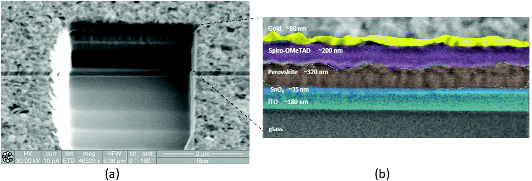 | ||
| Fig. 1 (a) Ion images of FIB cross section of a typical device; (b) enlarged image of the cross section and thickness of different layers measured by FIB. | ||
3. Results and discussion
J–V characteristics and PV parameters for pristine and stored PSCs
Two batches of devices, completed inside the GB and outside the GB, were fabricated on the same day with RH = (30 ± 10)% at 20 °C. Solar cells, after the first electrical measurement, were initially stored for 312 h in the dark and in a box with (30 ± 10)% relative humidity and monitored over time.When a decrease in the cell efficiency was recorded, the devices were placed in a low vacuum chamber (P ∼ 100 mbar) and measured over time again.
The last J–V measurements were performed after 720 h from the fabrication day and after low vacuum exposure. The J–V characteristics of the devices were always measured in humid air for both the batches of devices, constantly monitored but not controlled. In Fig. 2 and 3, the box plot charts of the normal distribution of PSCs are reported for all the PV parameters. In Tables S2 and S3 (ESI†), the average and champion values of each parameter measured over time for both the batches are reported. In the tables, the error values are reported as the standard deviations of three to ten devices averaged together for Voc and Jsc data, while the error propagation was reported for FF and PCE.
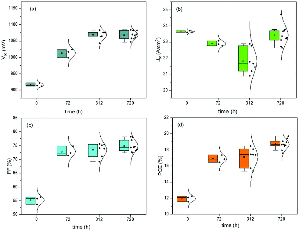 | ||
| Fig. 2 Box plot charts of normal distribution of PV parameters monitored over time for devices completed outside the GB. Pristine devices were measured at time 0, then stored in humid air for 312 h, and measured over time at 72 h and 312 h. Finally, the devices were inserted into a low vacuum chamber and measured at 720 h from the fabrication day. | ||
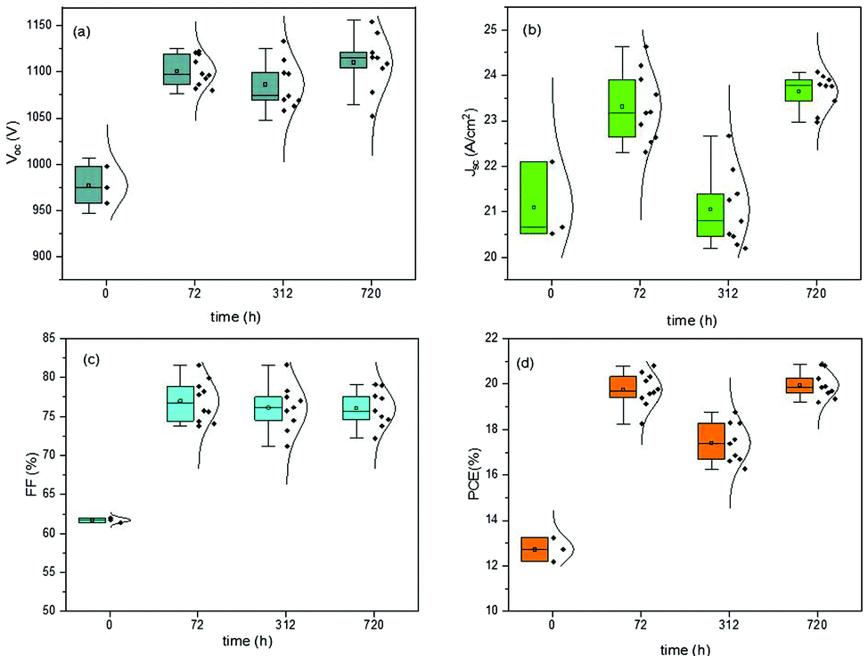 | ||
| Fig. 3 Box plot charts of normal distribution of PV parameters monitored over time for devices completed inside the GB. Pristine devices were measured at time 0, then stored in humid air for 312 h, and measured over time at 72 h and 312 h. Finally, the devices were inserted into a low vacuum chamber and measured at 720 h from the fabrication day. | ||
Furthermore, the oxygen present in the low vacuum chamber continuously improved the interface recombination between the perovskite/HTM and HTM/gold, thereby increasing the Voc. Finally, the best efficiency was obtained for the devices fabricated completely inside the nitrogen-filled glove box and after storage in humid air/low vacuum, for a total period of 720 h from the fabrication day. The batch of PSCs completed outside the GB confirmed the results discussed previously. This set of devices, having been exposed to humid air before gold evaporation, showed a high value of pristine Jsc, probably caused by the doping of water molecules incorporated into the perovskite bulk. As we formerly expected, after 72 h in humid air, this batch of devices completed outside the GB also exhibited a higher Voc, taking part in the oxidation of HTM, and consequently, a higher PCE. An interesting stability in performance was noted after 312 h in humid air and a decrease in PCE was not observed. However, also for these devices, after storage in a low vacuum chamber, PCE improvement was observed, confirming that reversible hydration was also present.5 In Fig. 4, the J–V curves over the storage time of the champion perovskite devices of the two different batches completed inside (Fig. 4a) and outside the GB (Fig. 4b) monitored over time are shown.
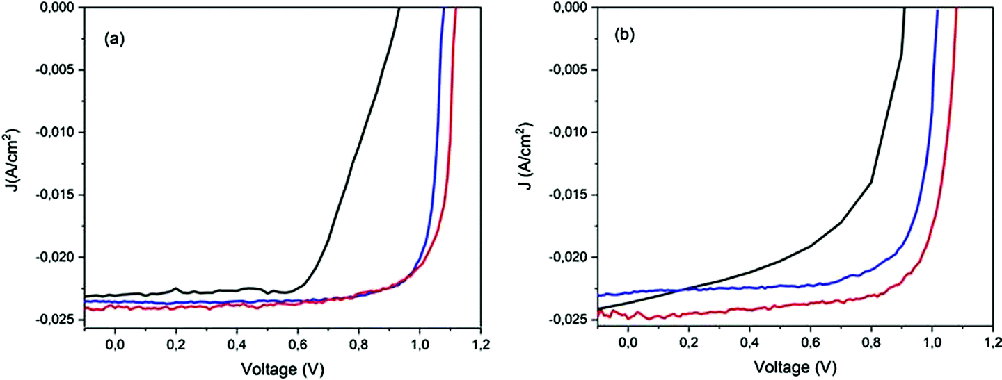 | ||
| Fig. 4 J–V curves acquired over time, before and after storage, for champion devices: pristine (black line), at 72 h (blue line) and at 720 h (red line) from device fabrication day (a) completely inside the GB and (b) outside the GB. | ||
The SEM and EDX elemental mapping of the perovskite film confirmed that moisture changed both the morphology and the bulk composition of the perovskite layer after exposure to humid air before gold evaporation (Fig. 5a, a1 and a2). More grains with smaller areas were observed when the perovskite absorber was exposed to humid air before gold evaporation (Fig. 5a and Fig. S4, ESI†), while larger grain areas were observed (Fig. 5b) when the cells were completed inside the GB. This feature could at least partially explain the better performance of these PSCs.57,58 A proof that oxygen was deeply incorporated into the devices completed outside the GB, and then stored in humid air before gold evaporation, was given from EDX mapping. The presence of oxygen, among the atoms, in the devices exposed to air, before gold evaporation, evidenced the presence of probable hydrate compounds (Fig. 5a1). Moreover, after one storage cycle in low vacuum, only a small reduction of oxygen occurred (Fig. 5a2). Meanwhile, the devices completed inside the glove box, after storage in humid air and low vacuum, did not show the presence of oxygen in the structure, demonstrating a non-significant absorption (Fig. 5b1 and b2).
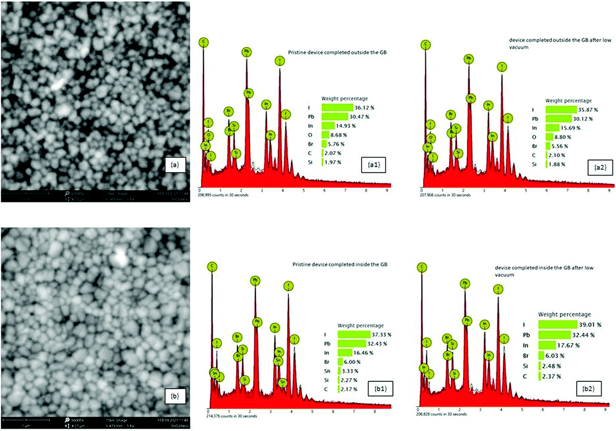 | ||
| Fig. 5 SEM images of perovskite layers (a) after exposure to humid air before gold evaporation for devices completed outside the GB and (b) for devices completed inside the GB immediately after gold deposition. EDX mapping and weight percentage of elemental atoms of pristine devices completed outside the glove box (a1) and after one air/vacuum cycle (a2); pristine devices completed inside the glove box (b1) and after one air/vacuum cycle (b2). | ||
Hysteresis-free behaviour of aged PSCs after storage
Typical hysteresis graphs were shown for the pristine and stored devices after humid air and low vacuum storage (Fig. 6). The J–V data of the pristine devices exhibited a large discrepancy (Fig. 6a) between the reverse and forward scan directions, which decreased after 72 h in humid air (Fig. 6b). A hysteresis-free behaviour was observed for all the devices after 720 h, after a cycle of humid air and low vacuum exposure (Fig. 6c and d). The J–V hysteresis is a dynamic process which can be influenced by both pre-conditions and measurement conditions, and by material properties such as the crystallite size of the perovskite layer and the interfaces between the absorber and the electron/hole transport materials.59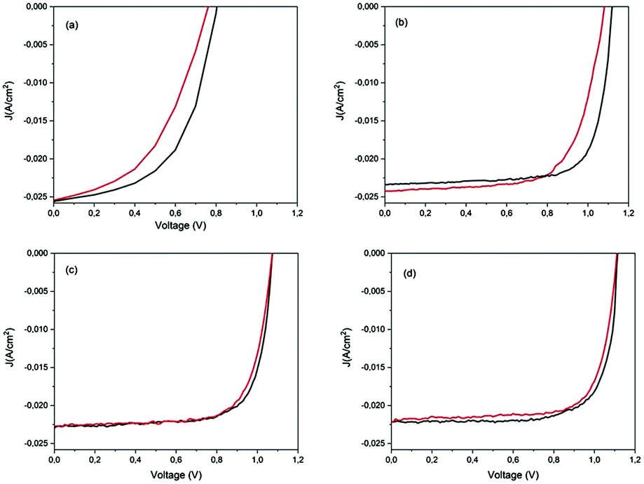 | ||
| Fig. 6 Reverse (dark line) and forward (red line) scans for hysteresis behaviour: (a) pristine PSCs, (b) after 72 h of storage in dark and in humid air, (c) and (d) after 720 h from the fabrication day for devices completed outside and inside the GB, respectively. | ||
In our case, the reduction of hysteresis was dependent on the storage conditions and not on the measurement procedures because the scan rate was always the same and the applied pre-bias was settled to 1.2 V close to Voc. Humid air improves the HTM conductivity and also balances the charge transport between the electrons and holes in the ETM and HTM, thereby reducing the number of surface traps and consequently reducing the hysteresis.
Dark J–V and ideality factor
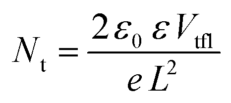
The absence of hysteresis over time allowed a more in-depth evaluation of the diode characteristics with and without illumination. The dark current–voltage curves for four different devices, completed both inside and outside the GB, recorded after 720 h from the fabrication day, are displayed in Fig. S5 (ESI†).When the current starts to increase in a non-linear way, the trap filling process is activated. The kink point between the linear region and the non-linear one is defined using the trap-filled limit voltage (Vtfl) and it is possible to calculate the trap density, according to the space-charge-limited current (SCLC) model, using the equation:60
 | (1) |
 | ||
| Fig. 7 Dark J–V measurements of the devices displaying the Vtfl kink point. | ||
The devices completed inside the GB, after 720 h, have a smaller trap density compared to the devices completed outside the GB. Then, the increase in Voc for the first batch during the storage time is probably due to the decrease in trap density. Probably, the incorporation of water molecules into the devices completed inside the glove box, after gold deposition and filling of deep charge carrier traps, reduces the defects and improves the conductivity of the HTM. However, water molecules incorporated into the devices completed outside the GB, before gold evaporation, leaves rather a larger trap density.
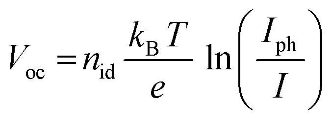
In order to investigate the recombination mechanism of the stored devices, illumination-dependent photovoltaic parameters were measured. To obtain the light-intensity dependent measurements, a set of neutral density filters was used, tuning the AM1.5 light of the solar simulator. The measurements were recorded at 1 sun (100 mW cm−2) and also at 0.4, 0.25, 0.16, 0.1 and 0.03 sun. The recombination was then investigated using the diode ideality factor (nid) extracted from the current–voltage curves measured at the slope of Voc as a function of illumination intensity. Identifying the ideality factor is a reliable way to indicate the dominant recombination mechanism of a solar cell which can be categorized into trap-assisted and bimolecular recombination.63–66 Tress et al.62 summarized that the ideality factor (nid) of PSCs is reliably obtained by light-intensity-dependent Voc measurements because measurements performed using an open circuit are not affected by the parasitic series resistance. For these measurements, nid can be calculated using the linear fit of the Voc as a function of ln(Iph/I) under relative light intensities using the equation:
 | (2) |
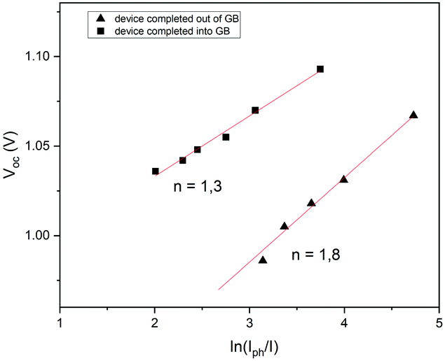 | ||
| Fig. 8 Intensity-dependent Voc for devices completed inside and outside the GB. | ||
To gain insights into charge recombination, we also studied the variation of Jsc as a function of illumination intensity (Fig. S6, ESI†). Many authors have observed a power-law dependence of Jsc upon light intensity (Jsc ∼ Jph ∼ Iα, where Jph is the photocurrent, I is the light intensity and α typically ranges ≤1). A value of α close to 1 indicates weak bimolecular recombination and non-space-charge limited devices, while the deviation of α from unity could be attributed to the bimolecular recombination, space-charge effects and variations in mobility between the holes and electrons.68 The preliminary results show the coefficient α to be 0.76 for the devices completed outside the GB (Fig. S6a, ESI†) and 0.81 for the devices completed inside the GB (Fig. S6b, ESI†), showing sublinear dependence less marked for the second one, probably evidencing a weak bimolecular recombination. These preliminary results are calculated for the devices stored in ambient air showing that the phenomenon of charge recombination depends not only on aging but also on the manufacturing environment, i.e. if the PSCs were exposed to air before or after gold evaporation. All the aged devices were in any case hysteresis-free, and probably, the increase of performances was due to the lower migration of ions and consequently, due to the less charge recombination. The mechanism that rules these phenomena is not yet clear. It could probably be the oxygen or the water present in humid air that fills the deep charge carrier traps, as shown in this work, or it could be the lithium dopant from the HTM that could significantly dope the perovskite absorber layer through diffusion, as reported in a recent study where the authors studied this mechanism, monitoring over a three-day window, with a decrease of spontaneous non-radiative recombination from trap states, providing an increase of photovoltaic performances.70 Moreover, the improvement of PV performances, compared to fresh and aged devices, was just recently studied for all-inorganic perovskite solar cells. The authors showed that all deep defects were reduced after resting the perovskite films overnight probably due to the self-regulation mechanism, connected with the strain released over time, showing the suppression of hysteresis too.71 Immediate understanding of these mechanisms is not possible and a better insight is required to apply multiple dynamic processes under different operating conditions. Several studies have been conducted to measure the charge transfer process, such as time-of-flight secondary-ion mass spectrometry, glow discharge optical emission spectrometry, transient photovoltage decay measurements and electrochemical impedance spectroscopy.21,22,67,72–74 These analyses could give more information on charge transport in PSCs, especially when hysteresis-free devices are obtained. Further investigation is needed to study the devices stored in ambient air, adding information on charge recombination when PV parameters increase over time, by linking the results with fabrication and storage processes.
4. Conclusions
In summary, we studied the effects of humid air and low vacuum storage on un-encapsulated planar devices (glass/ITO/SnO2/triple cation perovskite/Spiro-OMeTAD/Au) fabricated completely inside a N2-filled glove box or with gold contacts deposited outside the glove box. When all the devices, independently of the fabrication procedure, are stored in humid air for 72 h, exposure to oxygen and moisture showed an electrical conductivity enhancement and consequently, an improvement in interface charge transfer. As a result, Voc and FF increased due to the faster charge extraction. The devices showed, after 312 h in humid air, a good stability (less than 5% change) for all the PV parameters, except for Jsc which decreased by about 10%. The subsequent storage in low vacuum preserved the PV performance of all the devices, removing partly the water molecules inside the cell and improving additionally the PV parameters. We found, for the first time, to the best of our knowledge, an impressive increase of power conversion efficiency (PCE) from 13.2% to 20.8% after 72 h of storage in humid air (RH = 30 ± 10%), and a slight increase to 20.9% after low vacuum storage and 720 h from the fabrication day, for PSCs fabricated completely in a nitrogen-filled glove box. Moreover, all the PV parameters increased after storage with the fill factor exceeding 80%, a short circuit current density of about 24 mA cm−2 and an open circuit voltage of 1121 mV, for the champion devices. The hysteresis-free behaviour was also observed for all the devices after 720 h. Preliminary studies on possible charge recombination mechanisms were presented which showed that the devices completed inside the glove box exhibited a weak bimolecular or band-to-band recombination which is confirmed from the higher values of Voc. Improvement of PV parameters of un-encapsulated pristine perovskite solar cells after storage cycles in moderate humid air and low vacuum exposure opens up a new route for following encapsulation procedures.Author contributions
Vera La Ferrara: conceptualization, investigation, formal analysis, writing – original draft, and writing – reviewing and editing. Antonella De Maria: investigation, and writing – reviewing and editing. Gabriella Rametta: investigation, and writing – reviewing and editing. Paola Delli Veneri: project administration, and writing – reviewing and editing.Conflicts of interest
There are no conflicts to declare.Acknowledgements
The authors would like to thank Dr Enrico La Manna, Dr Emanuele Calabrò and Prof. Aldo Di Carlo (Centre for Hybrid and Organic Solar Energy (CHOSE), Rome, Italy), Dr Gennaro Sannino (ENEA and University “Federico II” Naples, Italy) and Dr Annalisa Bruno (Energy Research Institute@NTU, Singapore and ENEA, Italy) for their preliminary insights into tin oxide and triple cation perovskite layers, Dr Luca Serenelli (ENEA, Italy) for software for electrical characterization, and Antonio Romano and Antonio Citarella (ENEA, Italy) for maintenance of measurement equipment and holder-mask manufacturing. This work was supported by the Italian Ministry of Economic Development in the Framework of the Operating Agreement with ENEA for Research on the Electric System.References
- M. Liu, M. B. Johnston and H. Snaith, Nature, 2013, 501, 395–398 CrossRef CAS PubMed.
- H. S. Kim, I. Mora-Sero, V. Gonzalez-Pedro, F. Fabregat-santiago, E. J. Juarez-Perez, N. G. Park and J. Bisquert, Nat. Commun., 2013, 4, 2242 CrossRef PubMed.
- J. J. Yoo, G. Seo, M. R. Chua, T. G. Park, Y. Lu, F. Rotermund, Y. Y. Kim, C. S. Moon, N. J. Jeon, J. P. Correa-Baena, V. Bulovic, S. S. Shin, M. G. Bawendi and J. Seo, Nature, 2021, 590, 587–593 CrossRef CAS PubMed.
- Best Research-Cell Efficiency Chart. https://www.nrel.gov/pv/cell-efficiency.html (accessed 25 March 2021).
- Z. Song, A. Abate, S. C. Watthage, G. K. Liyanage, A. B. Phillips, U. Steiner, M. Graetzel and M. J. Heben, Adv. Energy Mater., 2016, 6, 1600846 CrossRef.
- Z. Hawash, L. K. Ono and Y. Qi, Adv. Mater. Interfaces, 2016, 3, 1600117 CrossRef.
- M. F. M. Noh, N. A. Arzaee, I. N. N. Mumthas, N. A. Mohamed, S. N. F. M. Nasir, J. Safaei, A. R. B. M. Yusoff, M. K. Nazeeruddin and M. A. M. Teridi, J. Mater. Chem. A, 2020, 8, 10481–10518 RSC.
- M. A. Haque, A. Syed, F. H. Akhtar, R. Shevate, S. Singh, K. V. Peinemann, D. Baran and T. Wu, ACS Appl. Mater. Interfaces, 2019, 11, 29821–29829 CrossRef CAS PubMed.
- I. Mesquita, L. Andrade and A. Mendes, Sol. Energy, 2020, 199, 474–483 CrossRef.
- I. Mesquita, L. Andrade and A. Mendes, ChemSusChem, 2019, 12, 2186–2194 CrossRef CAS PubMed.
- E. Ugur, E. Alarousu, J. I. Khan, A. Vlk, E. Aydin, M. De Bastiani, A. H. Balawi, S. P. Gonzalez Lopez, M. Ledinský, S. De Wolf and F. Laquai, Sol. RRL, 2020, 4, 2000382 CrossRef CAS.
- H. A. Dewi, H. Wang, J. Li, M. Thway, R. Sridharan, R. Stangl, F. Lin, A. G. Aberle, N. Mathews, A. Bruno and S. Mhaisalkar, ACS Appl. Mater. Interfaces, 2019, 11, 34178–34187 CrossRef CAS PubMed.
- A. Al-Ashouri, E. Köhnen, B. Li, A. Magomedov, H. Hempel, P. Caprioglio, J. A. Márquez, A. B. M. Vilches, E. Kasparavicius, J. A. Smith, N. Phung, D. Menzel, M. Grischek, L. Kegelmann, D. Skroblin, C. Gollwitzer, T. Malinauskas, M. Jošt, G. Matič, B. Rech, R. Schlatmann, M. Topič, L. Korte, A. Abate, B. Stannowski, D. Neher, M. Stolterfoht, T. Unold, V. Getautis and S. Albrecht, Science, 2020, 370, 1300–1309 CrossRef CAS PubMed.
- G. Nogay, F. Sahli, J. Werner, R. Monnard, M. Boccard, M. Despeisse, F.-J. Haug, Q. Jeangros, A. Ingenito and C. Ballif, ACS Energy Lett., 2019, 4, 844–845 CrossRef CAS.
- E. Lamanna, F. Matteocci, E. Calabrò, L. Serenelli, E. Salza, L. Martini, F. Menchini, M. Izzi, A. Agresti, S. Pescetelli, S. Bellani, A. Easù Del Rìo Castillo, F. Bonaccorso, M. Tucci and A. Di Carlo, Joule, 2020, 4, 865–881 CrossRef CAS.
- Y. Zhang and N. G. Park, J. Mater. Chem. A, 2020, 8, 17420–17428 RSC.
- E. López-Fraguas, B. Arredondo, C. Vega-Colado, G. del Pozo, M. Najafi, D. Martín-Martín, Y. Galagan, J. M. Sánchez-Pena, R. Vergaz and B. Romero, Org. Electron., 2019, 73, 292–298 CrossRef.
- J. Choi, S. Song, M. T. Hörantner, H. J. Snaith and T. Park, ACS Nano, 2016, 10, 6029–6036 CrossRef CAS PubMed.
- F. Giordano, A. Abate, J. P. C. Baena, M. Saliba, T. Matsui, S. H. Im, S. M. Zakeeruddin, M. K. Nazeeruddin, A. Hagfeldt and M. Graetzel, Nat. Commun., 2016, 7, 10379 CrossRef CAS PubMed.
- B. Conings, L. Baeten, T. Jacobs, R. Dera, J. D’Haen, J. Manca and H. G. Boyen, APL Mater., 2014, 2, 081505 CrossRef.
- B. Wang, M. Zhang, X. Cui, Z. Wang, M. Rager, Y. Yang, Z. Zou, Z. L. Wang and Z. Lin, Angew. Chem., Int. Ed., 2020, 59, 1611 CrossRef CAS PubMed.
- X. Meng, X. Cui, M. Rager, S. Zhang, Z. Wang, J. Yu, Y. W. Harn, Z. Kang, B. K. Wagner, Y. Liu, C. Yu, J. Qiu and Z. Lin, Nano Energy, 2018, 52, 123 CrossRef CAS.
- Q. Jiang, L. Zhang, H. Wang, X. Yang, J. Meng, H. Liu, Z. Yin, J. Wu, X. Zhang and J. You, Nat. Energy, 2017, 2, 16177 CrossRef CAS.
- S. Albrecht, M. Saliba, J. P. Correa Baena, F. Lang, L. Kegelmann, M. Mews, L. Steier, A. Abate, J. Rappich, L. Korte, R. Schlatmann, M. K. Nazeeruddin, A. Hagfeldt, M. Grätzel and B. Rech, Science, 2016, 9(1), 81–88, 10.1039/C5EE02965A.
- L. V. Mercaldo, E. Bobeico, A. De Maria, M. Della Noce, M. Ferrara, V. La Ferrara, L. Lancellotti, G. Rametta, G. V. Sannino, I. Usatii and P. Delli Veneri, Proceedings in EU PVSEC 2021, 6–10 September 2021, submitted.
- T. S. Sherkar, C. Momblona, L. Gil-Escrig, J. Ávila, M. Sessolo, H. J. Bolink and L. J. A. Koster, ACS Energy Lett., 2017, 2, 1214–1222 CrossRef CAS PubMed.
- C. M. Wolff, P. Caprioglio, M. Stolterfoht and D. Neher, Adv. Mater., 2019, 31, 1902762 CrossRef CAS PubMed.
- K. Kobbekaduwa, S. Shrestha, P. Adhikari, E. Liu, L. Coleman, J. Zhang, Y. Shi, Y. Zhou, Y. Bekenstein, F. Yan, A. M. Rao, H. Tsai, M. C. Bead, W. Nie and J. Gao, Nat. Commun., 2021, 12, 16362021 Search PubMed.
- L. X. Shi, Z. S. Wang, Z. Huang, W. E. I. Sha, H. Wang and Z. Zhou, AIP Adv., 2018, 8, 025312 CrossRef.
- P. Zhao, B. J. Kim and H. S. Jung, Mater. Today Energy, 2018, 7, 267–286 CrossRef.
- X. Wu, L. Zhang, Z. Xu, S. Olthof, X. Ren, Y. Liu, D. Yang, F. Gao and S. (Frank) Liu, J. Mater. Chem. A, 2020, 8, 8313–8322 RSC.
- A. Abate, M. Saliba, D. J. Hollm, S. D. Stranks, K. Wojciechowski, R. Avolio, G. Grancini, A. Petrozza and H. J. Snaith, Nano Lett., 2014, 14, 3247–3254 CrossRef CAS PubMed.
- C. M. Wolff, L. Canil, C. Rehermann, N. N. Linh, F. Zu, M. Ralaiarisoa, P. Caprioglio, L. Fiedler, M. Stolterfoht, S. Kogikoski Jr, I. Bald, N. Koch, E. L. Unger, T. Dittrich, A. Abate and D. Neher, ACS Nano, 2020, 14, 1445–1456 CrossRef CAS PubMed.
- M. Moriya, D. Hirotani, T. Ohta, Y. Ogomi, Q. Shen, T. S. Ripolles, K. Yoshino, T. Toyoda, T. Minemoto and S. Hayase, ChemSusChem, 2016, 9, 2634–2639 CrossRef CAS PubMed.
- T. J. Jacobsson, J. P. Correa-Baena, E. H. Anaraki, B. Philippe, S. D. Stranks, M. E. F. Bouduban, W. Tress, K. Schenk, J. Teuscher, J. E. Moser, H. Rensmo and A. Hagfeldt, J. Am. Chem. Soc., 2016, 138, 10331–10343 CrossRef CAS PubMed.
- F. Liu, Q. Dong, M. K. Wong, A. B. Djurišić, A. Ng, Z. Ren, Q. Shen, C. Surya, W. K. Chan, J. Wang, A. M. C. Ng, C. Liao, H. Li, K. Shih, C. Wei, H. Su and J. Dai, Adv. Energy Mater., 2016, 6, 1502206 CrossRef.
- Y. X. Tian, A. Merdasa, E. Unger, M. Abdellah, K. Zheng, S. McKibbin, A. Mikkelsen, T. Pullerits, A. Yartsev, V. Sundstrom and I. G. Scheblykin, J. Phys. Chem. Lett., 2015, 6, 4171–4177 CrossRef CAS PubMed.
- A. Ng, Z. W. Ren, Q. Shen, S. H. Cheung, H. C. Gokkaya, S. K. So, A. B. Djurisic, Y. Y. Wan, X. J. Wu and C. Surya, ACS Appl. Mater. Interfaces, 2016, 8, 32805–32814 CrossRef CAS PubMed.
- Z. W. Ren, A. Ng, Q. Shen, H. C. Gokkaya, J. Wang, L. Yang, W. K. Yiu, G. Bai, A. B. Djurisic, W. W. F. Leung, J. H. Hao, W. K. Chan and C. Surya, Sci. Rep., 2014, 4, 6752 CrossRef PubMed.
- W. J. Yin, H. Chen, T. Shi, S. H. Wei and Y. Yan, Adv. Electron. Mater., 2015, 1, 1500044 CrossRef.
- J. Huang, S. Tan, P. D. Lund and H. Zhou, Energy Environ. Sci., 2017, 10, 2284–2311 RSC.
- Z. Song, N. Shrestha, S. C. Watthage, G. K. Liyanage, Z. S. Almutawah, R. H. Ahangharnejhad, A. B. Phillips, R. J. Ellingson and M. J. Heben, J. Phys. Chem. Lett., 2018, 9, 6312–6320 CrossRef CAS PubMed.
- Y. Li, X. Xu, C. Wang, C. Wang, F. Xie, J. J. Yang and Y. Gao, J. Phys. Chem. C, 2015, 119, 23996–24002 CrossRef CAS.
- R. Long, W. Fang and O. V. Prezhdo, J. Phys. Chem. Lett., 2016, 7, 3215–3222 CrossRef CAS PubMed.
- X. Wang, H. Sarvari, H. Dang, Z. Chen and V. Singh, Optik, 2017, 150, 111–116 CrossRef CAS.
- Y. Cho, H. Do Kim, J. Zheng, J. Bing, Y. Li, M. Zhang, M. A. Green, A. Wakamiya, S. Huang, H. Ohkita and A. W. Y. Ho-Baillie, ACS Energy Lett., 2021, 6, 925–933 CrossRef CAS.
- F. Matteocci, L. Cina, E. Lamanna, S. Cacovich, G. Divitini, P. A. Midgley, C. Ducati and A. Di Carlo, Nano Energy, 2016, 30, 162–172 CrossRef CAS.
- F. Corsini and G. Griffini, J. Phys. Energy, 2020, 2, 031002 CrossRef CAS.
- Y. Lv, H. Zhang, R. Liu, Y. Sun and W. Huang, ACS Appl. Mater. Interfaces, 2020, 12, 27277–27285 CrossRef CAS PubMed.
- M. Saliba, T. Matsui, J. Y. Seo, K. Domanski, J. P. Correa-Baena, M. K. Nazeeruddin, S. M. Zakeeruddin, W. Tress, A. Abate, A. Hagfeldtd and M. Grätzel, Energy Environ. Sci., 2016, 9, 1989–1997 RSC.
- M. Saliba, J.-P. Correa-Baena, C. M. Wolff, M. Stolterfoht, N. Phung, S. Albrecht, D. Neher and A. Abate, Chem. Mater., 2018, 30, 4193–4201 CrossRef CAS.
- E. Enz, V. La Ferrara and G. Scalia, ACS Nano, 2013, 7, 6627–6635 CrossRef CAS PubMed.
- Q. Wang, B. Chen, Y. Liu, Y. Deng, Y. Bai, Q. Dong and J. Huang, Energy Environ. Sci., 2017, 10, 516–522 RSC.
- G. E. Eperon, S. N. Habisreutinger, T. Leijtens, B. J. Bruijnaers, J. J. van Franeker, D. W. deQuilettes, S. Pathak, R. J. Sutton, G. Grancini, D. S. Ginger, R. A. J. Janssen, A. Petrozza and H. J. Snaith, ACS Nano, 2015, 9, 9380–9393 CrossRef CAS PubMed.
- A. Abate, T. Leijtens, S. Pathak, J. Teuscher, R. Avolio, M. E. Errico, J. Kirkpatrik, J. M. Ball, P. Docampo, I. McPhersonc and H. J. Snaith, Phys. Chem. Chem. Phys., 2013, 15, 2572–2579 RSC.
- P. Caprioglio, M. Stolterfoht, C. M. Wolff, T. Unold, B. Rech, S. Albrecht and D. Neher, Adv. Energy Mater., 2019, 9, 1901631 CrossRef.
- X. Guo, C. McCleese, W. Gao, M. Wang, L. Sang and C. Burda, Mater. Renewable Sustainable Energy, 2016, 5, 17 CrossRef.
- S. Moghadamzadeh, I. M. Hossain, M. Jakoby, B. A. Nejand, D. Rueda-Delgado, J. A. Schwenzer, S. Gharibzadeh, T. Abzieher, M. R. Khan, A. A. Haghighirad, I. A. Howard, B. S. Richards, U. Lemmer and U. W. Paetzold, J. Mater. Chem. A, 2020, 8, 670–682 RSC.
- G. A. Nemnes, C. Besleaga, A. G. Tomulescu, L. N. Leonat, V. Stancu, M. Florea, A. Manolescu and I. Pintilie, J. Mater. Chem. C, 2019, 7, 5267–5274 RSC.
- R. H. Bube, J. Appl. Phys., 1962, 33, 1733–1737 CrossRef CAS.
- R. A. Awni, Z. Song, C. Chen, C. Li, C. Wang, M. A. Razooqi, L. Chen, X. Wang, R. J. Ellingson, J. V. Li and Y. Yan, Joule, 2020, 4, 644–657 CrossRef CAS.
- W. Tress, M. Yavari, K. Domanski, P. Yadav, B. Niesen, J. P. Correa Baena, A. Hagfeldt and M. Graetzel, Energy Environ. Sci., 2018, 11, 151–165 RSC.
- P. Calado, D. Burkitt, J. Yao, J. Troughton, T. M. Watson, M. J. Carnie, A. M. Telford, B. C. O'Regan, J. Nelson and P. R. F. Barnes, Phys. Rev. Appl., 2019, 11, 044005 CrossRef CAS.
- J. P. Correa-Baena, S. H. Turren-Cruz, W. Tress, A. Hagfeldt, C. Aranda, L. Shooshtari, J. Bisquert and A. Guerrero, ACS Energy Lett., 2017, 2, 681–688 CrossRef CAS.
- O. J. Sandberg, A. Sundqvist, M. Nyman and R. Österbacka, Phys. Rev. Appl., 2016, 5, 044005 CrossRef.
- L. J. A. Koster, V. D. Mihailetchi, H. Xie and P. W. M. Blom, Appl. Phys. Lett., 2005, 87, 203502 CrossRef.
- A. Mahapatra, N. Parikh, P. Kumar, M. Kumar, D. Prochowicz, A. Kalam, M. M. Tavakoli and P. Yadav, Molecules, 2020, 25, 2299 CrossRef CAS PubMed.
- L. J. Koster, V. D. Mihailetchi, H. Xie and P. W. Blom, Appl. Phys. Lett., 2005, 87, 203502 CrossRef.
- Q. Jiang, L. Zhang, H. Wang, X. Yang, J. Meng, H. Liu, Z. Yin, J. Wu, X. Zhang and J. You, Nat. Energy, 2017, 2, 16177 CrossRef CAS.
- C. Xiao, F. Zhang, Z. Li, S. P. Harvey, X. Chen, K. Wang, C.-S. Jiang, K. Zhu and M. Al-Jassim, Matter, 2020, 2, 261–272 CrossRef.
- Z. Yao, Z. Xu, W. Zhao, J. Zhang, H. Bian, Y. Fang, Y. Yang and S. (Frank) Liu, Adv. Energy Mater., 2021, 11, 2100403 CrossRef CAS.
- Z. Li, C. Xiao, Y. Yang, S. P. Harvey, D. Kim, J. A. Christians, M. Yang, P. Schulz, S. U. Nanayakkara, C. S. Jiang, J. M. Luther, J. J. Berry, M. C. Beard, M. M. Al-Jassim and K. Zhu, Energy Environ. Sci., 2017, 10, 1234–1242 RSC.
- H. Lee, S. Gaiaschi, P. Chapon, A. Marronnier, H. Lee, J.-C. Vanel, D. Tondelier, J.-E. Boureé, Y. Bonnassieux and B. Geffroy, ACS Energy Lett., 2017, 2, 943–949 CrossRef CAS.
- A. Pockett and M. J. Carnie, ACS Energy Lett., 2017, 2(7), 1683–1689 CrossRef CAS.
- Q. Jiang, Z. Chu, P. Wang, X. Yang, H. Liu, Y. Wang, Z. Yin, J. Wu, X. Zhang and J. You, Adv. Mater., 2017, 29, 1703852 CrossRef PubMed.
Footnote |
| † Electronic supplementary information (ESI) available. See DOI: 10.1039/d1ma00345c |
| This journal is © The Royal Society of Chemistry 2021 |