
 Open Access Article
 This Open Access Article is licensed under a
 Creative Commons Attribution 3.0 Unported Licence
p-Type molecular doping by charge transfer in halide perovskite†
Julie
Euvrard
 a,
Oki
Gunawan
b,
Xinjue
Zhong
c,
Steven P.
Harvey
d,
Antoine
Kahn
c and
David B.
Mitzi
*ae
a,
Oki
Gunawan
b,
Xinjue
Zhong
c,
Steven P.
Harvey
d,
Antoine
Kahn
c and
David B.
Mitzi
*ae
aDepartment of Mechanical Engineering and Materials Science, Duke University, Durham, North Carolina 27708, USA. E-mail: david.mitzi@duke.edu
bIBM T. J. Watson Research Center, Yorktown Heights, NY, 10598, USA
cDepartment of Electrical and Computer Engineering, Princeton University, Princeton, NJ, 08544, USA
dNational Renewable Energy Laboratory, Golden, CO 80401, USA
eDepartment of Chemistry, Duke University, Durham, North Carolina 27708, USA
First published on 30th March 2021
Abstract
Electronic technologies critically rely on the ability to broadly dope the active semiconductor; yet the promising class of halide perovskite semiconductors so far does not allow for significant control over carrier type (p- or n-) and density. The molecular doping approach offers important opportunities for generating free carriers through charge transfer. In this work, we demonstrate effective p-doping of MAPb0.5Sn0.5I3 films using the molecular dopant F4TCNQ as a grain boundary coating, offering a conductivity and hole density tuning range of up to five orders of magnitude, associated with a 190 meV Fermi level down-shift. While charge transfer between MAPb0.5Sn0.5I3 and F4TCNQ appears efficient, dopant ionization decreases with increasing Pb content, highlighting the need for appropriate energy offset between host and dopant molecule. Finally, we show that electrical p-doping impacts the perovskite optoelectronic properties, with a hole recombination lifetime increase of over one order of magnitude, suggesting passivation of deep traps.
Introduction
Tuning the carrier density from highly n-doped to highly p-doped enables effective semiconductor–metal interfaces, improved transport properties and flexibility in the design of various optoelectronic devices. As new generations of semiconductors emerge, targeting low-cost, large-area, flexible and semi-transparent applications, intensive efforts are being pursued to achieve such targeted control over properties.1–3 Electrical doping in organic semiconductors started initially with exposure to halogen vapors,4,5 later improved with the use of molecular dopants to provide extra carriers to the semiconductor host through a charge transfer process.6–8 Evidence of strong doping in halide perovskites has also been obtained early in the emergence of the halide perovskite field for optoelectronic applications, with semi-metallic conductivities reached for tin-based compounds, and attributed to the propensity of Sn2+ to oxidize to Sn4+.9,10 Unfortunately, precisely and effectively tuning the doping type and level in tin and other halide perovskites has proven particularly challenging and remains a significant bottleneck in the development of perovskite-based technologies.Taking advantage of the experience acquired from doping inorganic and organic semiconductors, various doping strategies have been explored and tested in halide perovskites, including intrinsic defect engineering through precursor ratio variations and extrinsic defect doping.3 However, the extent of achievable doping seems limited by the strong tendency of halide perovskites to compensate charged defects.11,12 Molecular doping appears among the most promising techniques for perovskites, with early works suggesting efficient tuning of the carrier properties at the film surface through charge transfer with a sequentially-deposited molecular layer.13,14 Yet, more homogeneous perovskite doping with molecular dopants is still in its infancy, showing only modest conductivity improvements.15–18 Doping of a particular perovskite host through charge transfer requires appropriate selection of the molecular dopant. p-Type doping can occur if the lowest unoccupied molecular orbital (LUMO) of the molecular dopant lies near or below the valence band maximum (VBM) of the perovskite host. 2,3,5,6-Tetrafluorotetracyanoquinodimethane (F4TCNQ) with a LUMO level at approximately −5.24 eV relative to the vacuum level19 is a widely studied electron acceptor for prospective p-doping of organic semiconductors7,20–24 and more recently halide perovskites.15,17,18 In previous studies, F4TCNQ introduced in MAPbI3 and CsPbI3 nanoparticles has shown a limited p-doping impact, potentially due to the inadequate energy level alignment, given reported ionization energies (IE) of 5.2 eV and 5.81 eV for MAPbI3 and CsPbI3 nanoparticles, respectively.15,17
Here we demonstrate efficient interfacial p-doping in a halide perovskite using molecular dopants directly interspersed in the perovskite precursor solution. To achieve appropriate energy level alignment for charge transfer with F4TCNQ, Pb is blended with Sn to form MAPb1−xSnxI3, leading to a decrease in IE with increasing Sn content (Fig. 1a).25,26 Employing x = 0.5, we show for the first time a tuning range of up to 5 orders of magnitude for halide perovskite conductivity using a molecular dopant. AC Hall effect measurements provide evidence of electrical doping, yielding hole carrier densities from ∼1013 cm−3 to ∼1017 cm−3. p-Doping is further confirmed through measurement of a Fermi level (EF) shift toward the perovskite VBM, along with an increase in work-function (WF), as observed using ultraviolet photoemission spectroscopy (UPS) and Kelvin probe-based contact potential difference (KP-CPD) measurements. The dopant molecules are shown to localize at the perovskite grain boundaries and throughout the film thickness using time-of-flight secondary-ion mass spectroscopy (TOF-SIMS) 3D tomography. Fourier transform infrared spectroscopy (FTIR) measurements support F4TCNQ ionization and confirm the reduced charge transfer efficiency with increased Pb content (increase in the perovskite IE), highlighting the need for appropriate perovskite-dopant energy level alignment for effective doping. Finally, carrier-resolved photo-Hall (CRPH) measurements reveal a deep trap passivation effect from doping, with a hole (majority carrier) lifetime increasing by more than one order of magnitude in conjunction with the doping. These results highlight the potential of molecular doping to effectively tune carrier density and optoelectronic properties in perovskites and open the door to future in-depth studies towards optimized perovskite doping.
 | ||
| Fig. 1 (a) Energy diagram of the MASn0.5Pb0.5I3 perovskite host and F4TCNQ molecular p-dopant, illustrating charge transfer from the top of the perovskite valence band (EV) to the LUMO of the dopant. Upon efficient charge transfer, the Fermi level EF is shifted toward the valence band. The perovskite EV is measured by UPS in this study. (b) MAPb0.5Sn0.5I3 conductivity for different F4TCNQ molar ratio (MR) concentrations. Several samples have been measured for each dopant concentration and the box charts indicate the maximum and minimum values (whiskers), the upper quartile and lower quartile (box) and the mean value (empty square). | ||
Results and discussion
F4TCNQ introduced within the MAPb0.5Sn0.5I3 film
In this study we introduce the molecular dopant, F4TCNQ, directly into the precursor solution, with an intent to spread the dopant throughout the thickness of the perovskite film as uniformly as possible. Fig. 1b displays the conductivity of the undoped and doped perovskite films with four F4TCNQ concentrations from 0.1% to 5% in molar ratio (MR). The film thicknesses needed for the conductivity calculations are extracted from SEM cross-section images (see Fig. S1, ESI†). A four-probe Hall bar method was used to prevent the influence of contact resistance on the conductivity extraction. Undoped MAPb0.5Sn0.5I3 exhibits a conductivity of between 10−6 and 10−5 S cm−1, about two orders of magnitude lower than values reported in the literature for mixed Pb–Sn compounds.27 Differences may arise due to variations in encapsulation quality, as this barrier prevents p-doping through Sn oxidation. Additionally, we noticed a persistent photocurrent effect, with pristine MAPb0.5Sn0.5I3 requiring about one hour in the dark to reach thermal equilibrium (Fig. S2, ESI†). Accordingly, one hour waiting time in the dark before measurement was implemented to ensure reliable dark measurements. Previous studies of conductivity and carrier density in mixed Sn/Pb perovskites may have been impacted by residual photogenerated carriers associated with the persistent photoconductivity effect. Through F4TCNQ doping, the conductivity can be tuned over four to five orders of magnitude, with a maximum conductivity of ∼10−1 S cm−1 obtained with 5% MR F4TCNQ.A significant improvement in conductivity only emerges for samples that were spin coated without the use of antisolvent, which exhibit large grain sizes (∼80 μm for the undoped samples) and incomplete surface coverage (Fig. 2). The perovskite film coverage of >79.5% (Fig. S3, ESI†), however, ensures reaching the percolation threshold (see ESI†), consistent with conductivity values orders of magnitude higher than for the bare glass substrate and epoxy glue. At dopant concentrations of 1% MR and above, darker areas attributed to F4TCNQ can be observed and enhanced in backscattered electron (BSE) SEM imaging mode (Fig. S4, ESI†). At 5% MR, we observe a strong impact of F4TCNQ inclusions on the perovskite morphology, suggesting that high concentrations of molecular dopants may disrupt crystal growth during film formation, possibly explaining the large variability in conductivity measurements for 5% MR doped samples (Fig. 1b).
 | ||
| Fig. 2 SEM images of MAPb0.5Sn0.5I3 with 0% (a; f), 0.1% (b; g), 0.2% (c; h), 1% (d; i) and 5% (e; j) F4TCNQ dopant, using an Everhart–Thornley detector with 100× magnification (a to e) and a Trinity detector with 5000× magnification collecting mostly secondary electrons (f to j). The scale bar is 500 μm for (a) to (e) and 10 μm for (f) to (j). | ||
To better identify the position of F4TCNQ molecules in the perovskite film, TOF-SIMS 3D tomography was performed on 1% doped MAPb0.5Sn0.5I3 samples (Fig. 3). In the summation intensity 2D images, we identify the fluorine signal (Fig. 3b) coming from F4TCNQ molecules, predominantly around the edges of the large grains (which are surrounded by uncoated glass) and also in what we believe are the true grain boundaries, which can be observed in the total signal image (Fig. 3a). The 3D tomography renderings (Fig. 3c and d) further indicate that F4TCNQ is not limited to the film surface, but occupies grain boundaries throughout the thickness of the perovskite film. Measurements were performed on an additional 1% doped sample (Fig. S5, ESI†) showing similar fluorine distribution, and on undoped MAPb0.5Sn0.5I3 (Fig. S6, ESI†) which exhibits uniform (background) fluorine distribution.
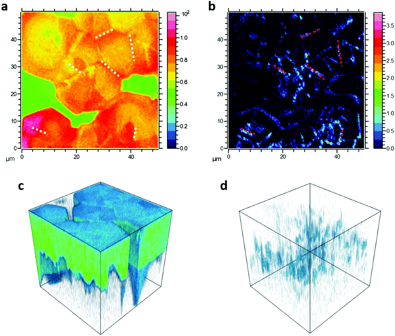 | ||
| Fig. 3 TOF-SIMS 2D images of 1% doped MAPb0.5Sn0.5I3 exhibiting the total signal (a) and the F signal (b). Each image is 50 × 50 μm and the color scale for each image shows the intensity in counts/pixel. The green area in panel (a) corresponds to uncoated glass substrate. White and red dotted lines are drawn as guide to the eye to show examples of grain boundaries visible in the total (a) and F (b) signals. TOF-SIMS 3D tomography rendering of the same dataset showing the signal coming from MA (MA: methylammonium), indicating the presence of the perovskite (c) and the F signal (d). Each 3D reconstruction is 50 × 50 × film thickness μm3. | ||
As shown in Fig. S7 (ESI†), no conductivity increase is measured for doped samples when chlorobenzene and toluene are used as antisolvents during film preparation, possibly due to the solubility of F4TCNQ in these solvents, which may lead to washing away of the dopant during the anti-solvent step. Alternatively, smaller grains (obtained with anti-solvent) are known to lead to a more rapid degradation of the MAPb0.5Sn0.5I3 samples,27 and could therefore account for the lower conductivity. Taking advantage of the wide grains obtained without antisolvent, we can process devices with sufficient stability (>8 days when encapsulated) for targeted characterization (see Fig. S8, ESI†).
Before attempting a deeper analysis to assess electrical doping and its impact on the perovskite optoelectronic properties, we confirmed with X-ray diffraction that no crystalline secondary phases are introduced in the structure and that no trend is observed in major diffraction peak positions with doping (see Fig. S9, ESI†). A slight change in preferred orientation is observed with 5% F4TCNQ, with an increased contribution along the (110) axis. The compositions of the undoped and doped perovskite films are determined from energy dispersive spectroscopy (EDS), yielding a Pb/Sn ratio of 1.1 ± 0.1 (Fig. S10, ESI†). UV-visible absorption spectroscopy was used to extract the perovskite film bandgap, yielding a constant value of 1.26 ± 0.01 eV from 0% to 5% MR (Fig. S11, ESI†), consistent with experimental and theoretical values reported in the literature for MAPb0.5Sn0.5I3.25,26,28
Electrical p-doping
We determine the energy levels at the surfaces of 0% and 1% doped MAPb0.5Sn0.5I3 films using ultraviolet photoelectron spectroscopy (UPS). By combining the WF deduced from the cut-off (Fig. 4a) and the VBM position with reference to the Fermi level EF (Fig. 4b), we extract the ionization energy of 5.11 eV for the pristine perovskite, defined as the energy difference between the vacuum level (Evac) and VBM. This confirms the expected VBM upshift with Sn content and the possibility for charge transfer, given the F4TCNQ LUMO at −5.24 eV.19 Upon addition of 1% MR F4TCNQ, a 190 meV shift of EF toward the VBM is observed while the IE remains unchanged at 5.12 eV (see schematic in Fig. 4c). A similar shift of the WF is observed using both UPS as well as KP-CPD measurements performed in the dark after one hour waiting time (Table S1, ESI†).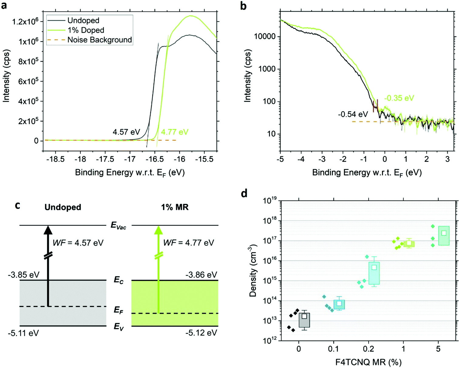 | ||
| Fig. 4 UPS spectra of the photoemission cut-off in linear scale (a) and the VBM edge in semi-logarithmic scale (b) for undoped and 1% doped MAPb0.5Sn0.5I3. The binding energy is with reference to the Fermi level. (c) Band diagram schematic of MAPb0.5Sn0.5I3 with 0% and 1% MR F4TCNQ. The VBM and WF are extracted from UPS measurements. The conduction band minimum EC is deduced from UPS and UV-visible absorption measurements considering a bandgap of 1.26 eV. EVac and EF correspond to the vacuum and Fermi levels, respectively. (d) Hole density of MAPb0.5Sn0.5I3 for different F4TCNQ concentrations in molar ratio (MR) obtained from AC Hall effect measurements. Several samples have been measured for each dopant concentration and the box charts indicate the maximum and minimum values (whiskers), the upper quartile and lower quartile (box) and the mean value (empty square). | ||
To further confirm and assess p-type doping in the bulk, we performed Hall effect measurements using a parallel dipole line (PDL) Hall system with a single harmonic AC magnetic field and distinguish the impact of hole density p and mobility μp on the increase in conductivity with F4TCNQ doping.29 The hole density and mobility are averaged over three to five samples per condition and are displayed in Fig. 4d and Fig. S12 (ESI†), respectively. An example of the Hall signal extraction is given in ESI† (Fig. S13) for an undoped sample. Pristine MAPb0.5Sn0.5I3 exhibits a hole density of (2 ± 1) × 1013 cm−3 and a hole mobility of 2.2 ± 0.9 cm2 V−1 s−1 after one hour waiting time in the dark. This relatively low carrier density shows that mixed Pb–Sn perovskite can reach close to intrinsic properties if Sn oxidation is properly prevented. The addition of F4TCNQ molecules effectively generates free holes in the perovskite film, with a hole density of (8 ± 4) × 1016 cm−3 reached with 1% MR F4TCNQ, while only a slight change is observed in the mobility. A carrier density of up to 5 × 1017 cm−3 can be obtained with 5% MR F4TCNQ (four order of magnitude enhancement over the undoped condition), however with substantial sample-to-sample variability, probably due to the strong film morphology disruption for this doping level (Fig. 2).
Dopant ionization
Upon charge transfer from host to dopant, we expect ionization of F4TCNQ. Ionized F4TCNQ generates specific signatures detectable using optical spectroscopy, given a sufficient concentration (>5–10%), as widely used to assess doping and its extent in organic semiconductors.7,30–32 The absorption features at ∼1.4–1.7 eV attributed to the anion F4TCNQ− interfere with the absorption of the perovskite host with a bandgap of 1.26 eV; however, the cyanovibrational bands of F4TCNQ can be detected using FTIR spectroscopy and provide information on the state of F4TCNQ.30,32 While undoped perovskite exhibits no visible peak in the range of interest, neutral F4TCNQ presents a characteristic peak at 2227 cm−1 corresponding to the b1u stretching mode (Fig. S14, ESI†).31 Upon complete ionization of the molecule to form the anion F4TCNQ−, we expect a shift toward 2194 cm−1.31 Intermediate shifts between neutral and fully ionized positions indicate partial ionization, revealing different degrees of charge transfer between 0 and 100%.30,33 The 5% MR doped MAPb0.5Sn0.5I3 exhibits a signal with multiple peaks that differ from the neutral molecules (Fig. 5a), confirming the existence of a charge transfer between the host and the dopant.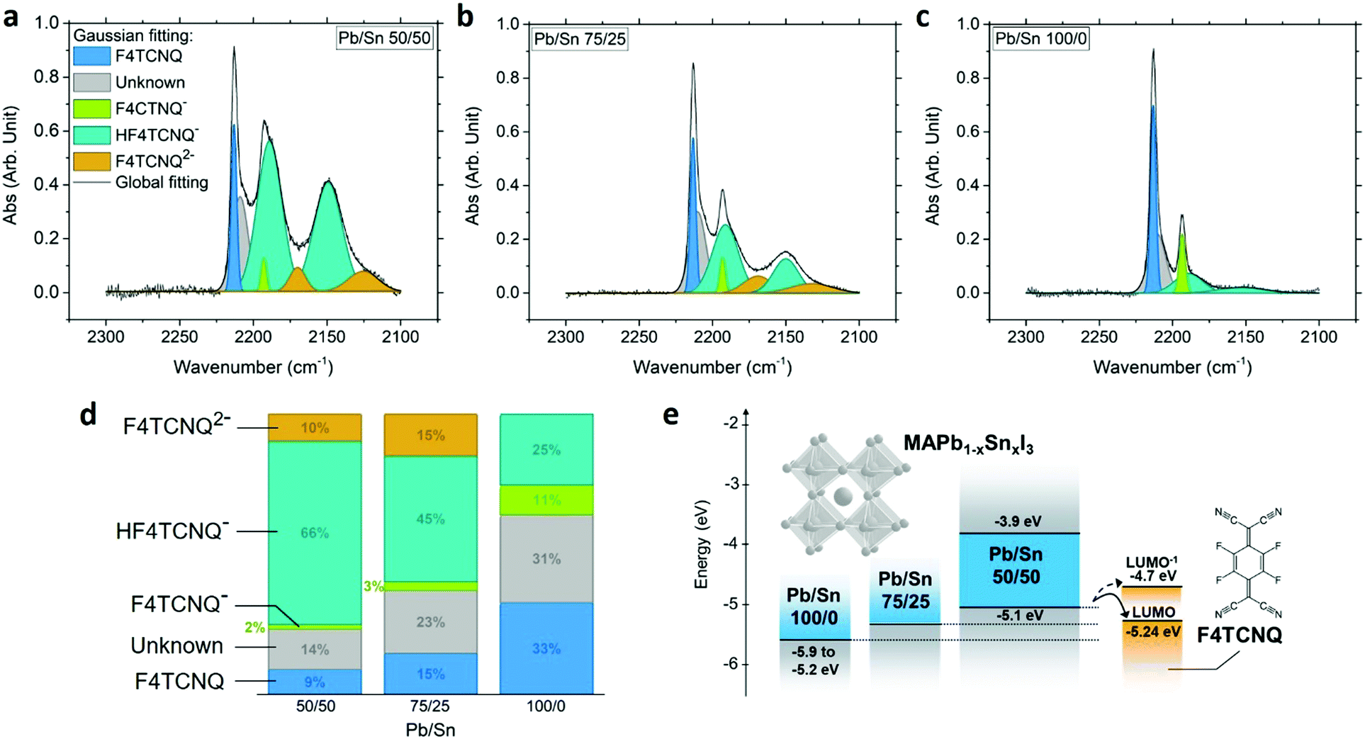 | ||
| Fig. 5 FTIR absorption spectra of the F4TCNQ cyano groups for 5% MR doped MAPb1−xSnxI3 with Pb/Sn ratio of 50/50 (x = 0.5) (a), 75/25 (x = 0.25) (b) and 100/0 (x = 0) (c). (d) Area under the curve associated with F4TCNQ, F4TCNQ−, HF4TCNQ−, F4TCNQ2− and an unknown component, from the Gaussian fitting of the FTIR spectra. See Fig. S15 (ESI†) for the extraction of peak position and area. (e) Energy diagram schematic showing the LUMO of neutral and singly ionized F4TCNQ (LUMO−),19,32 the VBM and CBM of MAPb0.5Sn0.5I3 from UPS and absorption measurements measured in this study, and a schematic view of the VBM evolution for MAPb0.75Sn0.25I3 and MAPbI3.25,26,38,39,60 | ||
A multiple Gaussian peak fitting is performed on the FTIR spectrum to identify the different components of the signal and determine their relative proportions, with a good fit achieved using seven peaks (Fig. S15, ESI†). While one peak positioned at ∼2209 cm−1 remains to be identified and could potentially be attributed to partial charge transfer, all other peaks correspond to known vibrational modes of F4TCNQ and its derivatives. The first sharp peak centered at 2213 cm−1 is attributed to the b2u mode of isolated neutral F4TCNQ,34 suggesting that neutral molecules remain in their isolated form (as opposed to crystalline form) in the final perovskite film. The peaks centered at ∼2193 cm−1 correspond to the b1u mode of fully ionized F4TCNQ (F4TCNQ−).31,34 Signal from the dianion F4TCNQ2− is also observed with broad peaks centered at ∼2170 and 2125 cm−1, attributed to the b1u and b2u + b3g modes.35 The formation of F4TCNQ anion and dianion confirms charge transfer with the perovskite host. Additionally, the FTIR spectrum provides evidence of the singly protonated monoanion HF4TCNQ− with two peaks at ∼2189 and 2150 cm−1.35,36 HF4TCNQ− can be obtained upon reaction of the dianion F4TCNQ2− with weak acids such as residual water.35,37 This reaction is further verified with successive FTIR measurements in air (Fig. S16, ESI†), showing a strong decrease of the F4TCNQ2− signal along with an increase in HF4TCNQ− signal. We therefore conclude that the HF4TCNQ− component results from dianion F4TCNQ2− degradation prior to measurement.
To evaluate the influence of the perovskite VBM position on doping efficiency, we performed FTIR measurements on 5% doped MAPb0.75Sn0.25I3 and MAPbI3 (Fig. 5b and c). A similar processing condition has been used and the corresponding XRD patterns and EDS analysis are provided in Fig. S17 (ESI†). With increasing Pb content we observe an increase in neutral F4TCNQ along with a decrease of the ionized and protonated F4TCNQ contributions (Fig. 5d), consistent with an increase in the perovskite IE with increasing Pb content and a less favorable charge transfer toward the LUMO of the neutral and monoanionic F4TCNQ around −5.24 eV and −4.7 eV, respectively (Fig. 5e).19,32 These data support the hypothesis of charge transfer and highlight the importance of relative energy level positions between the host and the molecular dopant, pointing to the need for a stronger oxidizing agent than F4TCNQ for the pure Pb compound MAPbI3 (IE ∼ 5.4 eV).38,39 We also note the change from yellow to green color of the MAPbI3 precursor solution upon F4TCNQ addition (Fig. S18, ESI†), while all solutions with Sn content remain orange (due to F4TCNQ). As solutions of MAI-F4TCNQ exhibit the same green color (Fig. S18e, ESI†), we hypothesize that the SnI2 precursor inhibits reaction between F4TCNQ and the precursor MAI. While this observation is beyond the scope of this study, it shows that further work is required to better understand the chemistry of the dopant-containing precursor solution before deposition and its potential impact on the final films.
Doping impact on optoelectronic properties
As electrical doping may influence semiconductor optoelectronic properties, we performed carrier-resolved photo-Hall (CRPH)40,41 measurements on undoped and 1% doped MAPb0.5Sn0.5I3 to assess the impact of F4TCNQ addition on carrier mobility, lifetime and diffusion length. The CRPH analysis relies on the evolution of the Hall coefficient H with conductivity σ obtained at different light intensities. Fig. S19 (ESI†) displays the H–σ evolutions for undoped and 1% doped MAPb0.5Sn0.5I3. The slope of the ln![[thin space (1/6-em)]](https://www.rsc.org/images/entities/char_2009.gif) H–lnσ curve (dlnH/dlnσ) is extracted to calculate the mobility difference Δμ:
H–lnσ curve (dlnH/dlnσ) is extracted to calculate the mobility difference Δμ: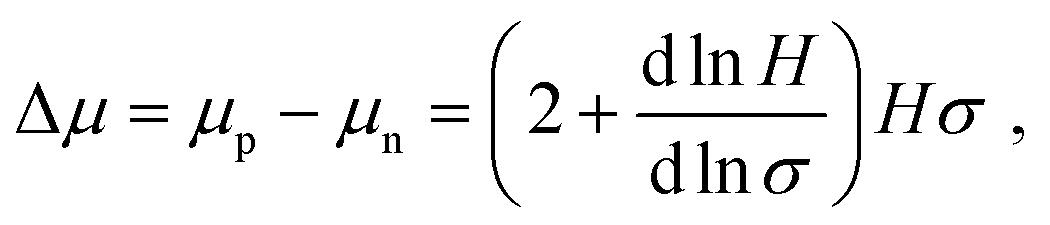 | (1) |
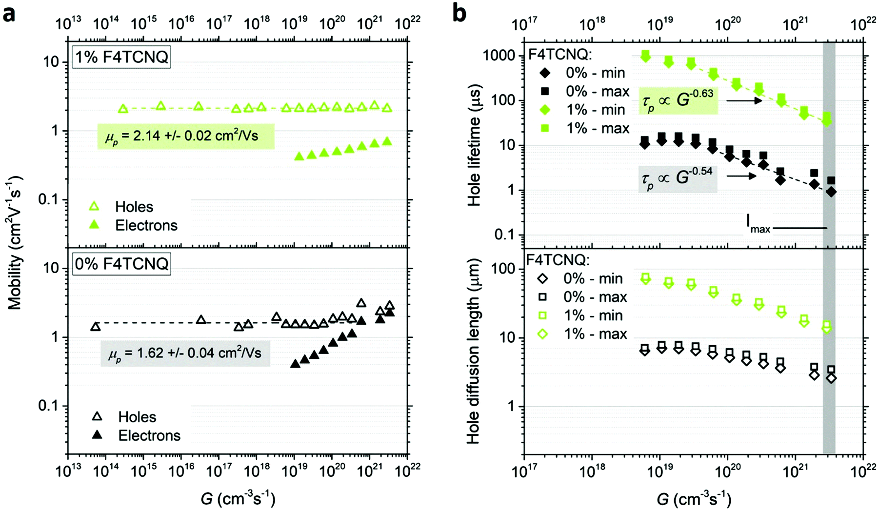 | ||
| Fig. 6 (a) Hole μp and electron μn mobilities as a function of generation rate G extracted from CRPH measurements for 0% and 1% doped MAPb0.5Sn0.5I3. (b) Hole lifetime τp and diffusion length Ld,p for 0% and 1% doped MAPb0.5Sn0.5I3. A linear fit at high light intensity follows a power law relationship τp ∝ Gγ−1. The grey area highlights the data points obtained at the highest light intensity Imax = 30 mW cm−2 (approximately a third of one sun intensity). | ||
The minimum and maximum values of the hole (majority carrier) recombination lifetime τp = Δp/G are calculated for both undoped and doped samples (Fig. 6b), showing a τp decrease with increasing light intensity as expected for majority carrier lifetime when electron traps are being filled.42 For both undoped and doped samples, the majority carrier lifetime decreases with generation rate following a power law with exponent γ−1 (τp ∝ Gγ−1) and γ values of 0.46 and 0.37 for 0% and 1% F4TCNQ, respectively. A value γ < 0.5 suggests the contribution of multiple trap levels in the semiconductor bandgap.42 An increase in hole recombination lifetime τp by one to two orders of magnitude can be observed with 1% F4TCNQ. This observation is consistent with higher photoconductivity with doping (see Fig. S20, ESI†) and suggests passivation of deep traps upon F4TCNQ addition. The hole diffusion length Ld,p can be calculated from μp and τp,
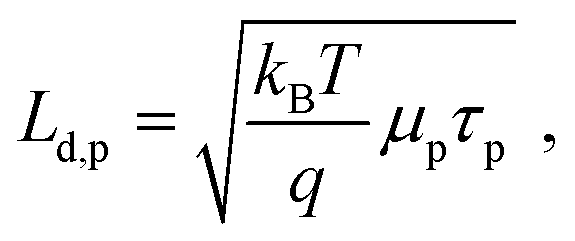 | (2) |
Conclusions
In this work, we show that effective electrical doping is possible in halide perovskites, given an appropriately chosen molecular dopant/perovskite host combination, carefully selected processing conditions, and an accounting for an often-neglected persistent photoconductivity effect. Conductivity tuning over five orders of magnitude has been obtained in MAPb0.5Sn0.5I3 using the molecular dopant F4TCNQ, localized at the perovskite grain boundaries throughout the film thickness as observed from TOF-SIMS tomography. The attribution of conductivity increase to doping is verified with AC Hall effect and UPS measurements, with the charge transfer process also being confirmed using FTIR through the detection of ionized F4TCNQ in the doped film. Moreover, we highlight the importance of relative perovskite VBM and dopant LUMO positions on the doping efficiency, with the pure lead MAPbI3 perovskite expected to be a less appropriate host for F4TCNQ. Finally, CRPH measurements reveal the impact of doping on the optoelectronic properties of the perovskite host, with an increase of the majority carrier lifetime by over one order of magnitude, presumably due to the passivation of deep traps in the mixed Pb/Sn perovskite.Therefore, molecular doping can be viewed as a promising avenue to finely tune electrical properties in halide perovskites, though further work is required to understand and optimize such processes for use in complete devices. Better processing techniques must be developed to deposit continuous and homogeneous doped perovskite films with smaller sample-to-sample variability. To achieve this goal, our understanding of the chemical and physical processes involved in the solution, during crystallization and in the final film must be improved. Additionally, we can expect to face impediments already encountered in organic semiconductor doping, including the formation of aggregates,43–48 instability,36,49–52 or limited doping efficiency.53–55 The latter issue is usually overcome with large concentrations of dopant (few %), which however can negatively impact the film morphology and could be particularly detrimental for crystalline halide perovskites, as observed in the present study for 5% doped MAPb0.5Sn0.5I3. As research progresses toward better control over the halide perovskite electronic properties, alternative molecular dopants with stronger oxidizing capabilities must be considered for compounds with deeper VBM. Additionally, bulk n-type doping should be explored to approach ambivalent properties and gain flexibility in the design of efficient devices.
Experimental section
Device fabrication
All samples were prepared through solution processing. 2,3,5,6-Tetrafluorotetracyanoquinodimethane (F4TCNQ, Sigma Aldrich) was initially dissolved in N,N-dimethylformamide (DMF, 99.8%, anhydrous, Sigma-Aldrich) and dimethyl sulfoxide (DMSO, 99.9%, anhydrous, Sigma-Aldrich) with a 8:2 volume ratio at concentrations of 2 to 10 mg mL−1 depending on the molar ratio targeted in the perovskite film. After one hour of stirring at room temperature, the appropriate volume of F4TCNQ solution was added to the precursors methylammonium iodide (MAI, Dyesol), lead iodide (PbI2, 99.99%, TCI chemicals) and tin(II) iodide (SnI2, anhydrous beads, 99.99%, Sigma Aldrich) to achieve F4TCNQ molar concentrations of 0.1%, 0.2%, 0.5%, 1% and 5%. DMF:DMSO (8:2) was added to achieve a perovskite molar concentration of 1.25 mol L−1. In the case of undoped MAPb0.5Sn0.5I3, only DMF:DMSO was used to dissolve the precursor powders. The solution was stirred at room temperature for one hour for all experiments to prevent any long-term impact of the solvent and reduce variability between experiments. The solutions were filtered using PTFE 0.2 μm filters and deposited within 30 min. Glass substrates were sonicated in deionized water, acetone, and isopropanol for 10 min each followed by a 10 min plasma etch treatment. Spin-coating was used to deposit undoped and doped MAPb0.5Sn0.5I3 solution (5000 rpm for 30 s) and no antisolvent was used during the spin-coating step. The films were annealed at 90 °C for 20 min. To achieve the large grains required to provide sufficient stability, deposition conditions (such as spin coating time) must be fine-tuned to allow crystallization of the film (change from yellow to dark brown color) on the hot plate (and not during spin-coating).
The Hall bars had six terminals with active area dimension of width × length = 2 × 4 mm and were patterned using a mask and a scalpel to remove the surrounding perovskite layer. Gold electrodes (100 nm) were deposited through a shadow mask by thermal evaporation using an Angstrom EvoVac evaporator operating at a base pressure below 2 × 10⁻⁶ torr. The Hall bars were encapsulated with glass using an epoxy glue (from Ellsworth) on the perimeter only. The entire fabrication was done in a nitrogen-filled glovebox with oxygen and water levels below 0.1 ppm.
Thin film characterization
X-ray diffraction (XRD) spectra were measured using a Panalytical Empyrean powder diffractometer with Cu Kα X-ray source and 45 kV/40 mA operating conditions. Top-view and cross-section scanning electron microscope (SEM) images were obtained using an Apreo S by ThermoFisher Scientific operated at 2 kV and 25 pA. Energy dispersive X-ray spectroscopy (EDX) was performed using an Oxford Instruments X-Max-N 150 SDD and an acceleration voltage of 15 kV. UV-vis and FTIR absorption spectroscopy were carried out with a Shimadzu UV-3600 spectrometer and a Thermo Electron Nicolet 8700 spectrometer, respectively. The reflectivity of the Hall bar sample, needed for the calculation of the generation rate, was obtained using an Enlitech QE-R Quantum Efficiency/Reflectivity system with integrating sphere. Current–voltage measurements were performed on Hall bars using a Keithley 4200-SCS analyzer.TOF-SIMS
An ION-TOF TOF-SIMS V spectrometer was utilized for depth profiling and chemical imaging of the perovskite utilizing methods covered in detail in previous reports.56–58 Analysis was completed utilizing a 3-lens 30 kV BiMn primary ion gun. High mass resolution depth profiles were completed with a 30 keV Bi3+ primary ion beam (0.8 pA pulsed beam current); a 50 × 50 μm area was analyzed with a 128:128 primary beam raster. 3-D Tomography and high-resolution imaging was completed with a 30 keV Bi3++ primary ion beam (0.1 pA pulsed beam current); a 50 × 50 μm area was analyzed with a 512:512 primary beam raster. In both cases the primary ion beam dose density was kept below 1 × 10¹²ions cm−2 to remain under the static-SIMS limit. Sputter depth profiling was accomplished with 1 kV Cesium ion beam (7 nA sputter current) with a raster of 150 × 150 microns.
Photoemission spectroscopy and Kelvin probe
Ultraviolet photoemission spectroscopy (UPS) measurements were performed in ultrahigh vacuum (10−10 torr) at room temperature. He I (21.22 eV) photons generated by a discharged lamp were used to probe the work function WF and valence band edges. Valence band spectra were recorded and plotted on a logarithmic intensity scale due to the low density of states near the band edge. Kelvin probe-based contact potential difference (KP-CPD) measurements were conducted in ultrahigh vacuum (10−8 torr) at room temperature in the dark. The CPD between the stainless-steel tip (4 mm) and the sample were recorded. The WF of the tip was calibrated before and after each measurement on a freshly cleaved highly ordered pyrolytic graphite (HOPG). The WF of HOPG was calibrated using UPS. All samples were spin-coated on indium tin oxide (ITO)/glass substrates, stored and transferred in N2 atmosphere without exposing to air.Dark Hall and carrier-resolved photo-Hall measurement
A parallel dipole line (PDL) Hall system was used to generate a unidirectional and pure single harmonic AC magnetic field monitored by a Hall sensor. The sample was mounted at the center of the PDL system where a magnetic field amplitude of 0.57 T is reached. A detailed description of the PDL Hall system can be found elsewhere.29 Light illumination using 638 nm (red) laser was used as light source. The light intensity was modulated over eight orders of magnitude using continuous neutral density filters with a maximum light intensity of 30 mW cm−2. A wedge lens was used to deflect the light beam onto the sample. A beam splitter was used to simultaneously illuminate the sample and a silicon photodetector to monitor the photocurrent at various light intensities and determine the incident absorbed photon density (Gγ) on the sample. A Keithley 2450 Source Meter Unit (SMU) was used to apply the current source and a Keithley 2001 Digital Multi Meter (DMM) for voltage measurement. A Keithley 7065 Hall switch matrix card with high impedance buffer amplifiers was used for routing the signals between the samples, the SMU and DMM. The current of the silicon photodetector was monitored using a Keithley 617 electrometer. The longitudinal and transverse (Hall) resistances from the Hall bars were measured from the minimum to the maximum brightness (to avoid the impact of persistent photoconductivity effects). The analysis of the Hall signal over time was performed using a custom-developed software developed in Matlab.59 A Fourier spectral analysis was performed on the Hall resistance after polynomial background subtraction to identify the Hall signal of the same frequency with the reference oscillating magnetic field. Finally, software lock-in detection was performed to extract the final Hall signal from the raw Hall resistance traces. We used a typical lock-in time constant of 120 s. Additional information on the photo-Hall setup and data analysis can be found elsewhere.40Author contributions
J. E. designed the study, prepared all samples, performed XRD, SEM/EDS, I–V measurements and UV-visible and FTIR spectroscopy, analyzed the dark Hall and CRPH measurements, and wrote the manuscript. O. G. collected the dark Hall and CRPH data and helped with the analysis and the manuscript. X. Z. performed UPS and KP measurements, analyzed the corresponding data and helped with the manuscript. S. H. performed 3D TOF-SIMS measurements, analyzed the corresponding data and helped with the manuscript. A. K. supervised UPS/KP and helped with the manuscript. D. B. M supervised the project and participated in the writing.Conflicts of interest
There are no conflicts to declare.Acknowledgements
This work was supported by the National Science Foundation under grant numbers DMR-2004869 and DMR-1709294. The work was performed in part at the Duke University Shared Materials Instrumentation Facility (SMIF), a member of the North Carolina Research Triangle Nanotechnology Network (RTNN), which is supported by the National Science Foundation (award number ECCS-2025064) as part of the National Nanotechnology Coordinated Infrastructure (NNCI). Work at Princeton University was supported by a grant from the US-Israel Binational Science Foundation (BSF Grant No. 2018349), and by a grant of the National Science Foundation (DMR-1807797). This work was authored in part by the National Renewable Energy Laboratory, operated by Alliance for Sustainable Energy, LLC, for the U.S. Department of Energy (DOE) under Contract No. DE-AC36-08GO28308. The TOF-SIMS was funded as part of the Center for Hybrid Organic Inorganic Semiconductors for Energy (CHOISE), an Energy Frontier Research Center funded by the U.S. Department of Energy, Office of Basic Energy Sciences (BES), Office of Science. The views expressed in the article do not necessarily represent the views of the DOE or the U.S. Government. The U.S. Government retains and the publisher, by accepting the article for publication, acknowledges that the U.S. Government retains a nonexclusive, paid-up, irrevocable, worldwide license to publish or reproduce the published form of this work, or allow others to do so, for U.S. Government purposes.Notes and references
- B. Lüssem, M. Riede and K. Leo, Phys. Status Solidi, 2013, 210, 9–43 CrossRef.
- M. Hiramoto, M. Kikuchi and S. Izawa, Adv. Mater., 2019, 31, 1801236 CrossRef PubMed.
- J. Euvrard, Y. Yan and D. B. Mitzi, Nat. Rev. Mater., 2021 DOI:10.1038/s41578-021-00286-z.
- C. K. Chiang, C. R. Fincher, Y. W. Park, A. J. Heeger, H. Shirakawa, E. J. Louis, S. C. Gau and A. G. MacDiarmid, Phys. Rev. Lett., 1977, 39, 1098–1101 CrossRef CAS.
- Y. Yamamoto, K. Yoshino and Y. Inuishi, J. Phys. Soc. Jpn., 1979, 47, 1887 CrossRef CAS.
- K. Walzer, B. Maennig, M. Pfeiffer and K. Leo, Chem. Rev., 2007, 107, 1233–1271 CrossRef CAS PubMed.
- I. E. Jacobs and A. J. Moulé, Adv. Mater., 2017, 29, 1703063 CrossRef PubMed.
- I. Salzmann and G. Heimel, J. Electron Spectrosc. Relat. Phenom., 2015, 204, 208–222 CrossRef CAS.
- D. B. Mitzi, C. A. Feild, Z. Schlesinger and R. B. Laibowitz, J. Solid State Chem., 1995, 114, 159–163 CrossRef CAS.
- D. B. Mitzi, C. A. Feild, W. T. A. Harrison and A. M. Guloy, Nature, 1994, 369, 467 CrossRef CAS.
- T. Shi, W. J. Yin, F. Hong, K. Zhu and Y. Yan, Appl. Phys. Lett., 2015, 106, 103902 CrossRef.
- T. Shi, W.-J. Yin and Y. Yan, J. Phys. Chem. C, 2014, 118, 25350–25354 CrossRef CAS.
- E. E. Perry, J. G. Labram, N. R. Venkatesan, H. Nakayama and M. L. Chabinyc, Adv. Electron. Mater., 2018, 4, 1800087 CrossRef.
- N. Noel, S. N. Habisreutinger, A. Pellaroque, F. Pulvirenti, B. Wenger, F. Zhang, Y.-H. Lin, O. Reid, J. Leisen, Y. Zhang, S. Barlow, S. R. Marder, A. Kahn, H. Snaith, C. Arnold and B. P. Rand, Energy Environ. Sci., 2019, 12, 3063 RSC.
- W. Q. Wu, Q. Wang, Y. Fang, Y. Shao, S. Tang, Y. Deng, H. Lu, Y. Liu, T. Li, Z. Yang, A. Gruverman and J. Huang, Nat. Commun., 2018, 9, 1625 CrossRef PubMed.
- H. Chen, Y. Zhan, G. Xu, W. Chen, S. Wang, M. Zhang, Y. Li and Y. Li, Adv. Funct. Mater., 2020, 30, 2001788 CrossRef CAS.
- E. A. Gaulding, J. Hao, H. S. Kang, E. M. Miller, S. N. Habisreutinger, Q. Zhao, A. Hazarika, P. C. Sercel, J. M. Luther and J. L. Blackburn, Adv. Mater., 2019, 31, 1902250 CrossRef PubMed.
- L. Zheng, T. Zhu, Y. Li, H. Wu, C. Yi, J. Zhu and X. Gong, J. Mater. Chem. A, 2020, 8, 25431–25442 RSC.
- W. Y. Gao and A. Kahn, J. Phys.: Condens. Matter, 2003, 15, S2757–S2770 CrossRef CAS.
- W. Gao and A. Kahn, Org. Electron., 2002, 3, 53–63 CrossRef CAS.
- W. Gao and A. Kahn, J. Appl. Phys., 2003, 94, 359–366 CrossRef CAS.
- K. H. Yim, G. L. Whiting, C. E. Murphy, J. J. M. Halls, J. H. Burroughes, R. H. Friend and J. S. Kim, Adv. Mater., 2008, 20, 3319–3324 CrossRef CAS.
- Y. Zhang, B. De Boer and P. W. M. Blom, Adv. Funct. Mater., 2009, 19, 1901–1905 CrossRef CAS.
- H. Kleemann, C. Schuenemann, A. A. Zakhidov, M. Riede, B. Lüssem and K. Leo, Org. Electron., 2012, 13, 58–65 CrossRef CAS.
- P. Kanhere, S. Chakraborty, C. J. Rupp, R. Ahuja and Z. Chen, RSC Adv., 2015, 5, 107497–107502 RSC.
- Y. Ogomi, A. Morita, S. Tsukamoto, T. Saitho, N. Fujikawa, Q. Shen, T. Toyoda, K. Yoshino, S. S. Pandey and S. Hayase, J. Phys. Chem. Lett., 2014, 5, 1004–1011 CrossRef CAS PubMed.
- M. Konstantakou and T. Stergiopoulos, J. Mater. Chem. A, 2017, 5, 11518–11549 RSC.
- S. Khatun, A. Maiti and A. J. Pal, Appl. Phys. Lett., 2020, 116, 012104 CrossRef CAS.
- O. Gunawan, Y. Virgus and K. F. Tai, Appl. Phys. Lett., 2015, 106, 062407 CrossRef.
- H. Méndez, G. Heimel, S. Winkler, J. Frisch, A. Opitz, K. Sauer, B. Wegner, M. Oehzelt, C. Röthel, S. Duhm, D. Többens, N. Koch and I. Salzmann, Nat. Commun., 2015, 6, 8560 CrossRef PubMed.
- P. Pingel, L. Zhu, K. S. Park, J. O. Vogel, S. Janietz, E. G. Kim, J. P. Rabe, J. L. Brédas and N. Koch, J. Phys. Chem. Lett., 2010, 1, 2037–2041 CrossRef CAS.
- D. Kiefer, R. Kroon, A. I. Hofmann, H. Sun, X. Liu, A. Giovannitti, D. Stegerer, A. Cano, J. Hynynen, L. Yu, Y. Zhang, D. Nai, T. F. Harrelson, M. Sommer, A. J. Moulé, M. Kemerink, S. R. Marder, I. McCulloch, M. Fahlman, S. Fabiano and C. Müller, Nat. Mater., 2019, 18, 149–155 CrossRef CAS PubMed.
- M. Meneghetti and C. Pecile, J. Chem. Phys., 1986, 84, 4149 CrossRef CAS.
- L. Zhu, E. Kim, Y. Yi and J.-L. Brédas, Chem. Mater., 2011, 23, 5149–5159 CrossRef CAS.
- K. E. Watts, K. E. Clary, D. L. Lichtenberger and J. E. Pemberton, Anal. Chem., 2020, 92, 7154–7161 CrossRef CAS PubMed.
- K. E. Watts, B. Neelamraju, M. Moser, I. McCulloch, E. L. Ratcliff and J. E. Pemberton, J. Phys. Chem. Lett., 2020, 11, 6586–6592 CrossRef CAS PubMed.
- T. H. Le, A. Nafady, X. Qu, L. L. Martin and A. M. Bond, Anal. Chem., 2011, 83, 6731–6737 CrossRef CAS PubMed.
- S. Olthof and K. Meerholz, Sci. Rep., 2017, 7, 40267 CrossRef CAS PubMed.
- J. Endres, D. A. Egger, M. Kulbak, R. A. Kerner, L. Zhao, S. H. Silver, G. Hodes, B. P. Rand, D. Cahen, L. Kronik and A. Kahn, J. Phys. Chem. Lett., 2016, 7, 2722–2729 CrossRef CAS PubMed.
- O. Gunawan, S. R. Pae, D. M. Bishop, Y. Virgus, J. H. Noh, N. J. Jeon, Y. S. Lee, X. Shao, T. Todorov, D. B. Mitzi and B. Shin, Nature, 2019, 575, 151 CrossRef CAS PubMed.
- J. Euvrard, O. Gunawan and D. B. Mitzi, Adv. Energy Mater., 2019, 9, 1902706 CrossRef CAS.
- I. Levine, S. Gupta, A. Bera, D. Ceratti, G. Hodes and H. J. Bolink, J. Appl. Phys., 2018, 124, 103103 CrossRef.
- I. E. Jacobs, E. W. Aasen, J. L. Oliveira, T. N. Fonseca, J. D. Roehling, J. Li, G. Zhang, M. P. Augustine, M. Mascal and A. Moule, J. Mater. Chem. C, 2016, 4, 3454–3466 RSC.
- K. Ferchichi, R. Bourguiga, K. Lmimouni and S. Pecqueur, Synth. Met., 2020, 262, 116352 CrossRef CAS.
- J. Euvrard, A. Revaux, P.-A. Bayle, M. Bardet, D. Vuillaume and A. Kahn, Org. Electron., 2018, 53, 135–140 CrossRef CAS.
- J. Gao, J. D. Roehling, Y. Li, H. Guo, A. J. Moulé and J. K. Grey, J. Mater. Chem. C, 2013, 1, 5638–5646 RSC.
- D. T. Scholes, S. A. Hawks, P. Y. Yee, H. Wu, J. R. Lindemuth, S. H. Tolbert and B. J. Schwartz, J. Phys. Chem. Lett., 2015, 6, 4786–4793 CrossRef CAS PubMed.
- F. M. McFarland, L. R. Bonnette, E. A. Acres and S. Guo, J. Mater. Chem. C, 2017, 5, 5764–5771 RSC.
- T. Nunes Domschke, O. Bardagot, A. Benayad, R. Demadrille, A. Carella, R. Clerc and A. Pereira, Synth. Met., 2020, 260, 116251 CrossRef CAS.
- M. L. Tietze, B. D. Rose, M. Schwarze, A. Fischer, S. Runge, J. Blochwitz-Nimoth, B. Lüssem, K. Leo and J. L. Brédas, Adv. Funct. Mater., 2016, 26, 3730–3737 CrossRef CAS.
- A. Dai, A. Wan, C. Magee, Y. Zhang, S. Barlow, S. R. Marder and A. Kahn, Org. Electron., 2015, 23, 151–157 CrossRef CAS.
- R. Kroon, D. Kiefer, D. Stegerer, L. Yu, M. Sommer and C. Müller, Adv. Mater., 2017, 29, 1700930 CrossRef PubMed.
- I. Salzmann, G. Heimel, M. Oehzelt, S. Winkler and N. Koch, Acc. Chem. Res., 2016, 49, 370–378 CrossRef CAS PubMed.
- P. Pingel and D. Neher, Phys. Rev. B: Condens. Matter Mater. Phys., 2013, 87, 115209 CrossRef.
- A. Mityashin, Y. Olivier, T. Van Regemorter, C. Rolin, S. Verlaak, N. G. Martinelli, D. Beljonne, J. Cornil, J. Genoe and P. Heremans, Adv. Mater., 2012, 24, 1535–1539 CrossRef CAS PubMed.
- S. P. Harvey, J. Messinger, K. Zhu, J. M. Luther and J. J. Berry, Adv. Energy Mater., 2020, 10, 1903674 CrossRef CAS.
- S. P. Harvey, F. Zhang, A. Palmstrom, J. M. Luther, K. Zhu and J. J. Berry, ACS Appl. Mater. Interfaces, 2019, 11, 30911–30918 CrossRef CAS PubMed.
- S. P. Harvey, Z. Li, J. A. Christians, K. Zhu, J. M. Luther and J. J. Berry, ACS Appl. Mater. Interfaces, 2018, 10, 28541–28552 CrossRef CAS PubMed.
- O. Gunawan and M. A. Pereira, US Pat. 9772385, 2017 Search PubMed.
- P. Schulz, E. Edri, S. Kirmayer, G. Hodes, D. Cahen and A. Kahn, Energy Environ. Sci., 2014, 7, 1377–1381 RSC.
Footnote |
| † Electronic supplementary information (ESI) available. See DOI: 10.1039/d1ma00160d |
| This journal is © The Royal Society of Chemistry 2021 |