DOI:
10.1039/D1MA00114K
(Paper)
Mater. Adv., 2021,
2, 3613-3619
Porous fibres of a polymer blend for broadband microwave absorption
Received
7th February 2021
, Accepted 29th March 2021
First published on 29th March 2021
Abstract
This study is on the advantages of introducing pores in polymer blend fibres in broadband microwave absorption. The electrospun porous and non-porous fibres of a blend, polyvinyl butyral and poly(3,4-ethylenedioxythiophene)polystyrene sulfonate-PEDOT:PSS (PPPS), are explored. The porous PPPS fibres (PPPS-f) demonstrated an outstanding reflection loss (RL) bandwidth (8.2–12.4 GHz, X-band) with a minimum RL of −23 dB, whereas the non-porous PPPS-f of the same thickness did not exhibit even adequate levels of RL. A high dielectric loss tangent and the electromagnetic attenuation constant (with a phase constant) are the major factors contributing to this difference. Additionally, impedance matching and the electromagnetic energy density are observed to be the major factors in porous PPPS-f achieving this excellent microwave absorption bandwidth, a finding supported by microwave simulation data. A bi-layer structure of porous PPPS-f and non-porous PPPS-f is also proposed to achieve an X-band absorption bandwidth at minimum thickness. An android mobile app is also developed to identify the RL of single and bi-layered porous PPPS-f and non-porous PPPS-f conveniently.
Introduction
Rapid growth in electronics, especially high-power electronic instruments, means more chances of electromagnetic signal interference,1–3 affecting not only humans but also the proper functioning of electronic devices and defense security devices that use the X-band (8.2–12.4 GHz) frequency.1,2 Great effort has been made to combat these interferences through various designs, such as by introducing magnetic and dielectric components, incorporation of morphological patterns, and using tailor-made materials,1–7 thus the need for apposite materials with electrical conductivity, multifunctionality, and processability. Polyvinylbutyral (PVB) has excellent moisture barrier properties and has received tremendous attention as a device encapsulation material, especially in organic electronics.4–6 Additionally, PVB is lightweight and has stretchability, which encompasses application areas such as portable electronics and wearable devices,7 whereas it lacks electrical conductivity. A recent investigation shows that the microwave dielectrics of a conducting polymer, poly(3,4-ethylenedioxythiophene)polystyrene sulfonate (PEDOT:PSS), based blend can be easily tuned, through various types of morphology.7,8
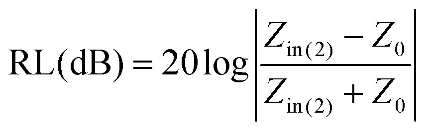
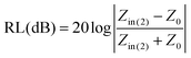
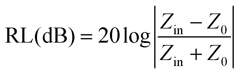
The microwave absorption property is understood in terms of reflection loss (RL), and it is expressed as (metal-backed),6–10
| | 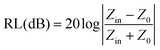 | (1) |
where
Z0 (= 377 Ω) is the free space intrinsic impedance and
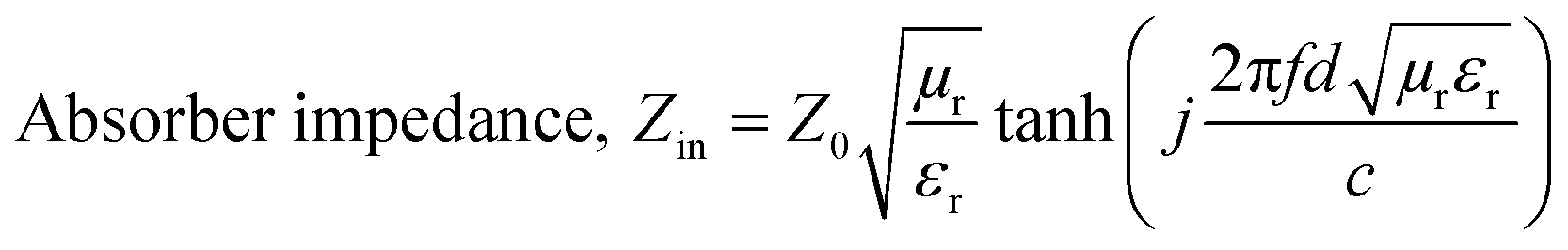
| |  | (2) |
where
εr is the relative permittivity (
εr =
ε − i
ε) and
μr is the relative permeability (
μr =
μ − i
μ) of the material (for a non magnetic material,
μ = 1 and
μ = 0),
f is the frequency,
d is the thickness of the single layer absorbing material, and
c is the velocity of light. For practical applications, the minimum RL value should be −10 dB, which corresponds to 90% absorption.
1
Various research groups have reported microwave absorption through morphology tuning.9–13 However, reports on absorption bandwidth (RL ≤ −10 dB) engineering through morphology tuning are very limited. To achieve the entire X-band RL ≤ −10 dB with a single layer is a challenge.9 Porous microwave dielectric materials are believed to be an ideal lightweight broadband microwave absorber.12,13 The key interest in porous materials for microwave absorption is that they can provide a better impedance matching degree and effective permittivity, multiple reflections, and high stored electromagnetic energy density, resulting in broadband absorption.10,14–16 The present work evaluates, for the first time, the effect of both morphological patterning, by creating pores on the surface of fibers, and the use of a novel polymer blend, PVB-PEDOT:PSS (PPPS), on the microwave absorption behavior. The porous fibers and non-porous solid fibres are fabricated through optimized electrospinning parameters.
Results and discussion
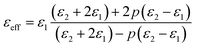
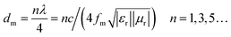
The schematic of the electrospinning setup for the non-porous PPPS fibres (non-porous PPPS-f) and porous PPPS fibres (porous PPPS-f) is shown in Fig. 1(a). The recorded SEM images of the electrospun non-porous PPPS-f are shown in Fig. 1(b). In Fig. 1(b), the PPPS-f obtained using isopropyl alcohol are non-porous, smooth with uniform surfaces, and have average diameters of 931 ± 11 nm. Fig. 1(c) shows the recorded SEM images of porous PPPS-f. The porous PPPS-f obtained using a solvent mixture of methanol and isopropyl alcohol (Fig. 1(c)) possess nanopores of irregular size and have diameters of 1030 ± 9 nm. These porous fibres are slightly larger than the non-porous ones and have striated surfaces. During the electrospinning of porous PPPS-f the methanol evaporates due to high vapour pressure, thus creating pores on the fibers and imparting a more irregular morphology.
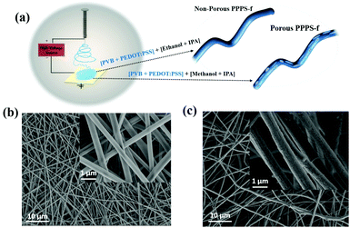 |
| | Fig. 1 (a) Schematic of the electrospinning setup for non-porous PPPS-f and porous PPPS-f. (b) Surface morphology of non-porous PPPS-f, and (c) surface morphology of porous PPPS-f. | |
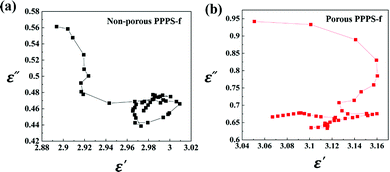
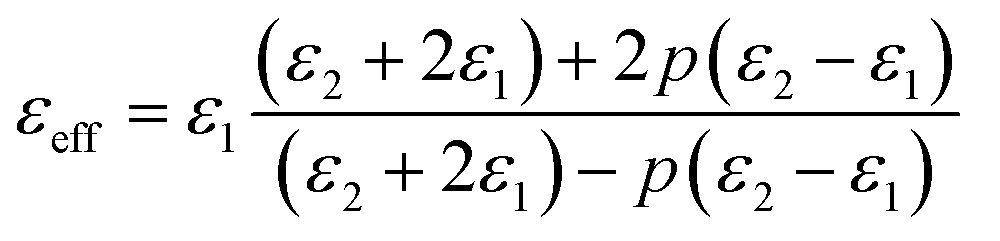
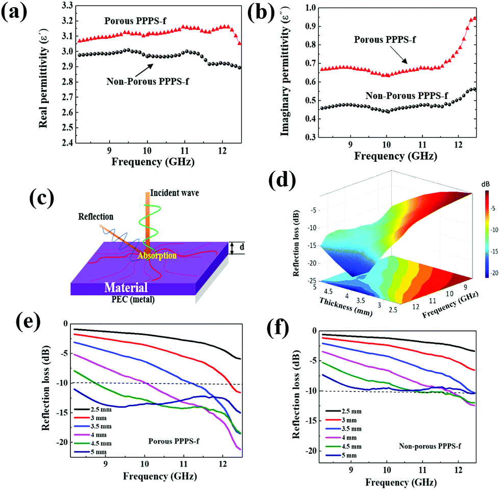
The variation of the electromagnetic parameters, viz., the real part of the permittivity, ε′ (corresponding to the storage ability of electric energy), and the imaginary part of the permittivity, ε′′ (corresponding to the dissipation of electric energy inside the material),4,6 of both porous and non-porous PPPS-f are shown in Fig. 2(a) and (b), respectively. In Fig. 2(a), the ε′ value (∼3.1) of the porous PPPS-f predominates over that of the non-porous PPPS-f. In Fig. 2(b), significant differences in the ε′′ values (across the X-band) are observed between the porous and non-porous PPPS-f. The recorded ε′′ values of the porous PPPS-f are in the range of 0.65–0.95, whereas those of the non-porous PPPS-f show less variation and are in the range of 0.45–0.55, in the frequency range of 8.2–12.4 GHz. The observed variation of the electromagnetic parameters is due to the non-linear phenomenon which is associated with charge polarization due to point effects, the skin effect, polarized centres and interfacial polarization.6–10 The interfacial polarization for the porous PPPS-f is expected to be higher than that of the non-porous PPPS-f, due to the presence of voids, and is approximated from the change of the ε′′ value i.e., Δε′′.10 The value of Δε′′ for the porous PPPS-f is ∼0.3, whereas for the non-porous PPPS-f it is ∼0.1, clearly indicating that interfacial polarization is prevalent in the porous PPPS-f. In comparison to ε′′ as observed, the variation in ε′ of both the porous and non-porous PPPS-f is not so effective. This lower variation in ε′ could be due to the presence of voids with a larger diameter in the porous PPPS-f.11 This variation can also be understood through Maxwell–Garnett (MG) theory,11 which indicates the medium's effective permittivity. According to MG theory, the effective permittivity (εeff) can be expressed as:11
| |  | (3) |
where
ε1 and
ε2 represent the permittivity of the solid-state and gas phase, respectively, and
p is the volume fraction of the guest in the effective medium. As for the gas phase, the permittivity is nearly 1; therefore, here
ε2 can be considered as 1. Thus, from
eqn (3), it is clear that
εeff will decrease with an increase in the void concentration. Hence, less pronounced variation is observed in the porous PPPS-f; in other words, the porous PPPS-f have better impedance matching properties.
 |
| | Fig. 2 Variation of the recorded (a) real permittivity and (b) imaginary permittivity of porous PPPS-f and non-porous PPPS-f in the X-band. (c) Schematic of the absorbing structure, and (d) 3D reflection loss (RL) plot of porous PPPS-f. Thickness dependent reflection loss (dB) of (e) porous PPPS-f and (f) non-porous PPPS-f. | |
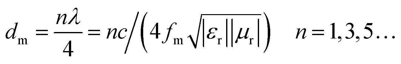
The microwave absorption properties of a material can be understood in terms of reflection loss (RL) for a perfect electric conductor (PEC) or metal backed condition,6–10 as shown in Fig. 2(c). The thickness-dependent 3D RL plot of the porous PPPS-f is shown in Fig. 2(d). Fig. 2(e) and (f) show the RL for different thicknesses (2.5–5 mm) of the porous and non-porous PPPS-f, respectively. The porous PPPS-f exhibit an optimum RL, with an excellent bandwidth (RL ≤ −10 dB). In fact, single-layer porous PPPS-f cover effective absorption for the entire X-band, with a minimum RL value (−15 dB), whereas no specific RL bandwidth is seen for the non-porous PPPS-f. For both the porous and non-porous PPPS-f, the variation of the RL in the X-band follows a nearly linear trend until 4 mm thickness. In the porous PPPS-f, the minimum RL values are −11 dB, −18 dB and −23 dB for thicknesses of 3 mm, 3.5 mm and 4 mm, respectively (Fig. 2(d and e)). Further observation shows that, as the thickness is increased to 5 mm, the minimum RL peak tends towards the low-frequency region. The RL fluctuation in Fig. 2(d–f) is due to the quarter wavelength resonance9–13 (arises due to geometrical or structural effects) and it can be correlated with a matching thickness (dm) and matching frequency (fm),
| |  | (4) |
From
eqn (4), it is clear that the optimal RL intrinsically depends on
dm and
fm, and for a particular pair (
dm,
fm) strong dissipation of the incident electromagnetic wave energy takes place resulting in excellent absorption.
9–13 In other words, for a particular thickness, the minimum RL value peak of the absorber (porous PPPS-f, non-porous PPPS-f) is associated with a specific frequency, and since
dm and
fm are inversely related, therefore, on increasing the thickness the RL peak shifts towards the low frequency region.
9–13
The density of the porous PPPS-f is less (0.39 g cm−3) than the non-porous PPPS-f (0.51 g cm−3); therefore, the specific RL (SRL) value, i.e., RLmin (RL ≤ −10 dB)/density, is very high for the porous PPPS-f. The factor SRL/thickness (d) is more realistic as it intrinsically depends on the RL, density and thickness of the absorption material.2 The obtained SRL/d of the porous PPPS-f is 102.5 dB cm2 g−1, whereas this factor is 0 for the non-porous PPPS-f (for 5 mm thickness) in the frequency range 8.2–12.4 GHz. Thus, it indicates the lightweight microwave absorption characteristics of the porous PPPS-f.
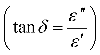
The major factors contributing in turn to this outstanding RL bandwidth of the porous PPPS-f are the dielectric loss tangent  , electromagnetic (EM) attenuation coefficient (α), phase constant (β), EM energy density and impedance matching.3–6 The tan
![[thin space (1/6-em)]](https://www.rsc.org/images/entities/char_2009.gif) δ values of both the porous and non-porous PPPS-f are shown in Fig. 3(a). In the X-band, the tanδ values range between 0.21 and 0.31 for the porous PPPS-f and 0.15 and 0.18 for the non-porous PPPS-f. Thus, the tanδ values for the porous PPPS-f are predominant and indicate high absorption capability.
δ values of both the porous and non-porous PPPS-f are shown in Fig. 3(a). In the X-band, the tanδ values range between 0.21 and 0.31 for the porous PPPS-f and 0.15 and 0.18 for the non-porous PPPS-f. Thus, the tanδ values for the porous PPPS-f are predominant and indicate high absorption capability.
 |
| | Fig. 3 Variation of the (a) dielectric loss tangent, (b) attenuation constant, (c) phase constant and (d) normalized EM energy density with respect to ε0|E0|2 of the porous PPPS-f and non-porous PPPS-f in the frequency range 8.2–12.4 GHz. CST-Microwave Studio simulated accepted power (PA) results for various thicknesses of the (e) porous PPPS-f and (f) non-porous PPPS-f in the frequency range 8.2–12.4 GHz (X-band). | |
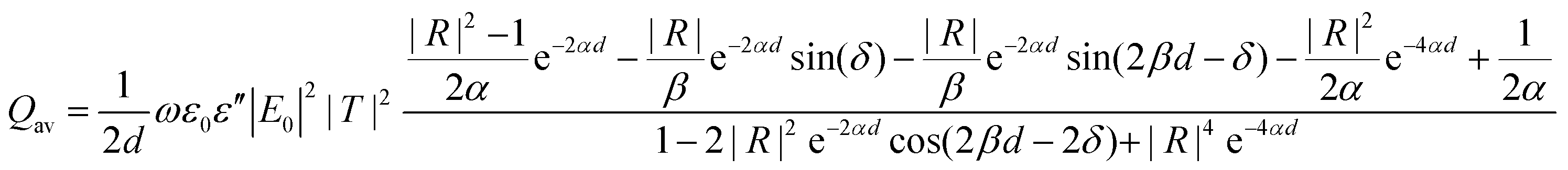
According to electromagnetic theory, the microwave power absorption per unit volume due to the dielectric loss (W m−3) can be expressed as17
| |  | (5) |
where
ω is the angular frequency,
E0 is the amplitude of the microwave electric field strength, and
T and
R are the transmission and reflection coefficients at the interface between free space and the magnetic dielectric medium, respectively.
α and
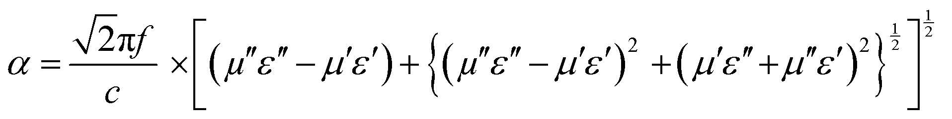
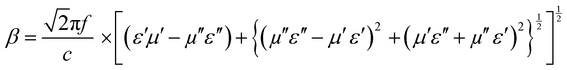
β are the electromagnetic (EM) field attenuation factor and phase constant, respectively, which can be expressed as,
17| | 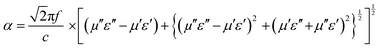 | (6) |
| | 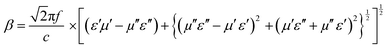 | (7) |
The calculated EM attenuation coefficient (
α)
3,6 values of both the porous and non-porous PPPS-f shown in
Fig. 3(b) are between 35 and 70 and 25 and 40, respectively. The tan
δ values of the porous PPPS-f are predominant; therefore, as expected, the
α values of the porous PPPS-f are also very high. Thus, excellent EM attenuation is taking place in the porous PPPS-f. The phase constant (
β) is also an important factor as the contribution of dielectric loss (
QE) to the microwave power absorption per unit volume (W m
−3) also depends on it.
17 The variation of the calculated
β value of the porous PPPS-f and non-porous PPPS-f is shown in
Fig. 3(c).
Fig. 3(c) indicates that the
β value of the porous PPPS-f (
β value range 330–500) is intrinsically predominant as compared to the non-porous PPPS-f (
β value is 320–470). Thus, the high
α and
β values indicate the high microwave power absorption density of the porous PPPS-f as compared to the non-porous PPPS-f. To determine the average power absorption density in the porous PPPS-f and non-porous-PPPS-f, the incident
E0 is assumed to be 4754 V m
−1 (commonly used for most microwave applications including household) for 8.2 GHz. The obtained
Qav of 5 mm thick porous PPPS-f and non-porous PPPS-f was 59052535.5 W m
−3 and 58275345.86 W m
−3 respectively. The difference in
Qav,
i.e., Δ
Qav, was found to be 777189.7 W m
−3, indicating excellent microwave power absorption characteristics of the porous PPPS-f.
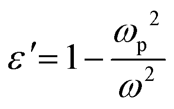
According to electromagnetism theory,18 the total electromagnetic energy density consists of two terms, viz., the stored electromagnetic energy density (us) and dissipated electromagnetic energy density (ud). Mathematically, it can be expressed as,18
| | 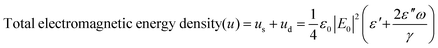 | (8) |
where
γ is the damping frequency. The
γ value can be calculated from the relations

and

, where
ωp parameterizes the interaction strength between the dipole oscillators in the medium and the electric field. The normalized electromagnetic energy density (
u) of the porous PPPS-f and non-porous PPPS-f is shown in
Fig. 3(d). The normalized
u value of the porous PPPS-f is higher than the non-porous PPPS-f. Thus, it indicates the high relative absorption bandwidth of the porous PPPS-f as compared to the non-porous PPPS-f. In order to validate the above discussion, standard EM simulations are carried out using CST-Microwave Studio [4, 6, and 9]. The resulting power levels accepted by both the porous and non-porous PPPS-f are shown in
Fig. 3(e) and (f), respectively. The simulation results indicate that the power accepted by the porous PPPS-f is greater than that for the non-porous PPPS-f, especially for the 5 mm thickness.
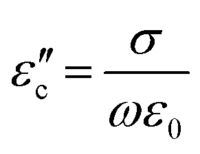
The loss mechanism of electromagnetic waves also can be understood from the EM power conversion due to the charge transport (Pc) and relaxation (Pp). Based on Debye theory,19,20 two factors, viz., εc′′ (corresponds to the contribution of charge transport to ε′′) and εp′′ (corresponds to the contribution of relaxation to ε′′), are considered, and ε′′ = εc′′ + εp′′. The Pc and Pp values intrinsically depend on εc′′ and εp′′, respectively. The εc′′ value19,20 depends on the electrical conductivity ( , σ is the conductivity).19,20 As shown in Fig. 4(a and b), the Cole–Cole plots show that in the porous PPPS-f semicircles (each semicircle corresponds to dielctric relaxation9,19) are observed. It suggests that εp′′ can not be ignored. Hence energy conversion due to dielectric relaxation is also an important factor in the porous PPPS-f, resulting in better absorption.
 |
| | Fig. 4 Cole–Cole plot of the (a) non-porous PPPS-f and (b) porous-PPPS-f. | |
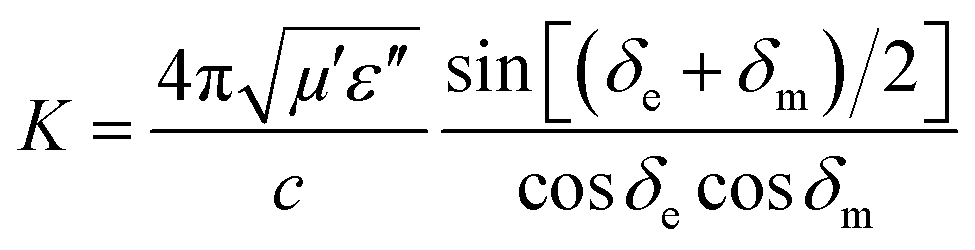
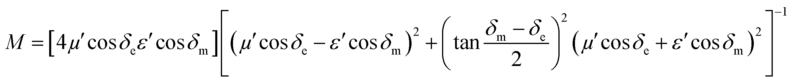
The high dielectric loss tangent and high EM-attenuation (α) are the key factors in the porous PPPS-f for excellent electromagnetic loss, resulting in a high electromagnetic power absorption density. However, the EM impedance matching is another key factor in the porous PPPS-f. The presence of nanopores in the PPPS-f leads to better EM impedance matching through the effective permittivity; consequently, it contributes to achieve a better RL.11 The relationship between the EM impedance matching degree (Δ) and RL value was reported by Zhai et al.21Δ is expressed as,21
where
K and
M depend on the relative complex permittivity and permeability as follows,
21| | 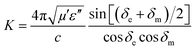 | (10) |
| | 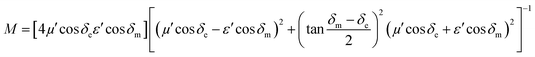 | (11) |
A smaller
Δ value implies better microwave absorption characteristics (or minimum RL value).
21 The calculated
Δ value for the porous PPPS-f (2–0.58) was found to be less than that for the non-porous PPPS-f (2.9–1.1) in the X-band for the studied thicknesses (1–5 mm). Thus, the obtained
Δ value analysis suggests that the porous PPPS-f possess better EM impedance matching and microwave absorption characteristics than the non-porous PPPS-f. Further, the presence of pores may lead to an additional pathway for electromagnetic energy losses.
12 This process can be understood through the antenna mechanism as well as through multiple reflections.
12 According to the antenna mechanism,
4,13 the incident microwave energy propagates through fibres in the form of a microcurrent, acting as a receiver antenna and transmitting the energy to the microcurrent. The presence of more nanopores (where the surface area to volume ratio is very high) increases the resistance in the fibres; therefore, energy is lost and is absorbed primarily throughout the porous PPPS-f. In addition, the existence of dihedral angles (created by the nanopores) in the porous PPPS-f may create the space for multiple reflections and thus increased the propagation paths of the microwaves in the absorber, resulting in more absorption.
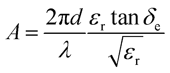
According to electromagnetic theory,22 the electromagnetic absorption coefficient (A) of a plane EM wave can be expressed as,22
| | 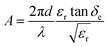 | (12) |
where
λ is the wavelength

.
Fig. 5(a) and (b) show the obtained
A values of the non-porous PPPS-f and porous PPPS-f, respectively. The
A value of non-porous PPPS-f was obtained to be 0.1–0.43 (for 1–5 mm thickness,
Fig. 5(a)). As shown in
Fig. 5(b), for 5 mm thick porous PPPS-f, the
A value lies in the range 0.35–0.73. A remarkable improvement of “
A” was found in the porous PPPS-f as compared to the non-porous PPPS-f. Thus, it reveals that the microwave absorption characteristics of the porous PPPS-f are much stronger than the non-porous PPPS-f.
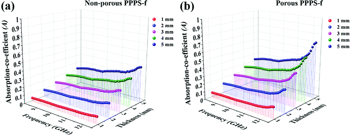 |
| | Fig. 5 Absorption coefficient (A) of the (a) non-porous PPPS-f and (b) porous PPPS-f in the X-band (8.2–12.4 GHz). | |
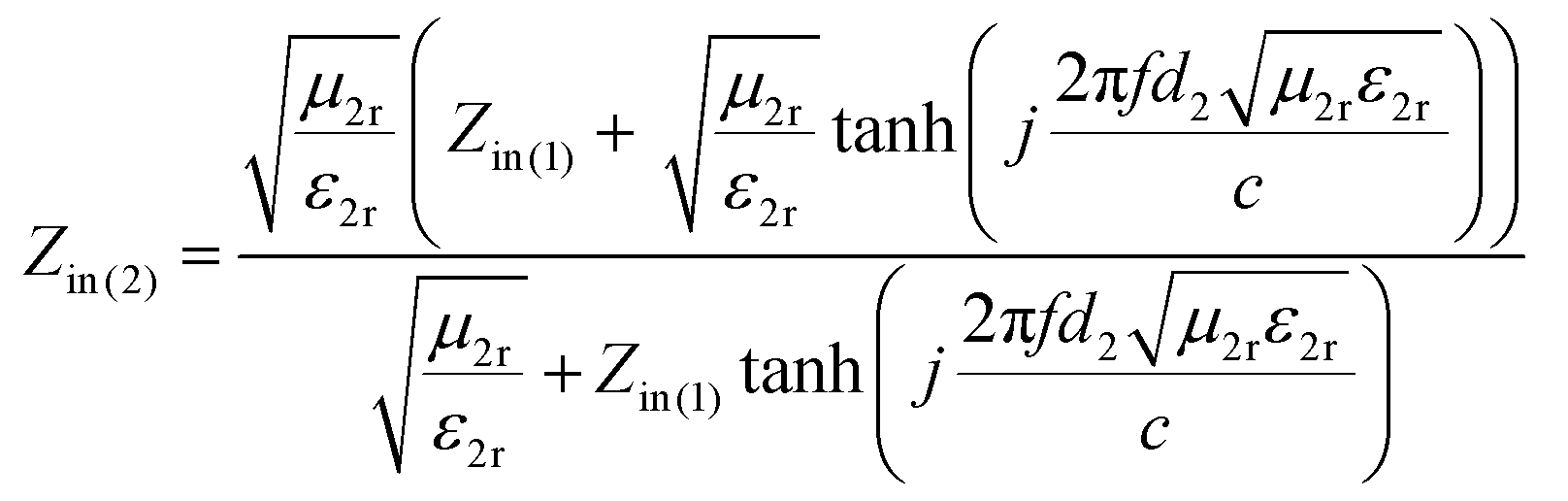
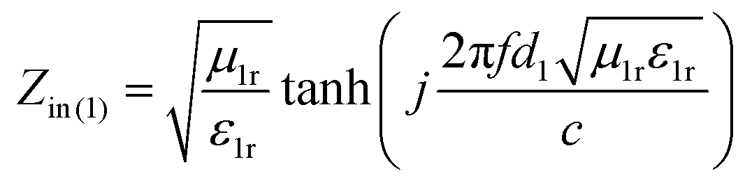
A tandem structure is preferred for high absorption with a high absorption bandwidth at minimum thickness.23–25 As a case study, a bi-layer structure of porous PPPS-f and non-porous PPPS-f is also studied. As shown in Fig. 6(a), the porous PPPS-f are on top with thickness d1 and the non-porous PPPS-f, having thickness d2, are kept at the bottom and are PEC or metal backed. The RL of this structure can be expressed as,24,25
| |  | (13) |
Here,
| | 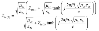 | (14) |
| | 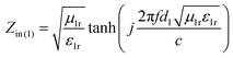 | (15) |
Here,
ε1r and
μ1r correspond to the relative permittivity and permeability of the
d1 layer and
ε2r and
μ2r correspond to the relative permittivity and permeability of the
d2 layer.
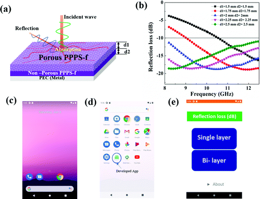 |
| | Fig. 6 (a) Schematic of the proposed bi-layer structure. (b) Reflection loss (dB) for different d1 and d2 values of the bi-layer structure in the frequency range 8.2–12.4 GHz. Screenshot of (c) the home page of the Google Pixel phone, (d) the developed app and (e) the app home page. | |
The obtained RL for different d1 and d2 values is shown in Fig. 6(b). The minimm RL value −19 dB is obtained with entire X-band absorption for d1 = 2 mm and d2 = 2 mm. Thus, it shows that a 4 mm thick bi-layer structure of porous PPPS-f (on top) and non-porous PPPS-f (bottom) exhibits an excellent absorption bandwidth (RL ≤ −10 dB) in the frequency range 8.2–12.4 GHz, which is comparatively less thick than a single layer of porous PPPS-f (5 mm).
In order to identify the RL value easily and quickly for different thicknesses of porous PPPS-f and non-porous PPPS-f, an android app is developed (for both single layer and bi-layer). The mobile application is created using Android Studio (2.3.3) which is based on Java programming. The screenshots (Google Pixel) of the developed mobile application are shown in Fig. 6(c–e).
Conclusions
Therefore, through this study, it can be said that the electrospun porous PPPS-f exhibit outstanding absorption bandwidth (RL ≤ −10 dB) across the entire X-band (8.2–12.4 GHz) of microwave absorption, with a minimum RL value of −23 dB for a 5 mm thickness. In contrast, for the same thickness, the non-porous PPPS-f reveal an inadequate RL value. The mechanisms studied indicate that both the dielectric loss tangent and the electromagnetic attenuation are intrinsically predominant in the porous PPPS-f. The microwave power absorption density due to the dielectric loss is very high for the porous PPPS-f as compared to the non-porous PPPS-f. Further, the presence of nanopores in the porous PPPS-f has contributed to impedance matching, multiple reflections and high stored electromagnetic energy density, resulting in excellent bandwidth. The microwave simulation data supports the experimental observation, implying that the porous structure fibre morphology can enhance the RL compared to the plain fibre morphology. The tandem structure of bi-layered porous PPPS-f and non-porous PPPS-f shows an excellent X-band absorption bandwidth at relatively lower thickness (4 mm), indicating a most promising porous PPPS-f and non-porous PPPS-f combination for efficient microwave absorption.
Experimental
PVB, purchased from Synpol Pvt. Ltd, is dissolved in solvents such as methanol and isopropyl alcohol (S D Fine Chem. Ltd) to obtain a 15% (w/v) solution. The solution is blended with 1 ml of PEDOT:PSS, purchased from Clevios Heraeus. The electrospinning is carried out at an applied voltage of 10 kV (source: Gamma DC high voltage instrument, USA) with a flow rate of 1 ml h−1 (maintained by a Holmarc SPLF-2D) and a tip-to-collector distance of 8 cm on an aluminum grounded collector for a period of 1 h. For the porous fibres a mixture of methanol and isopropyl alcohol (1:1) is used, whereas for the non-porous fibres only isopropyl alcohol is used. The surface morphology of the electrospun fibres is investigated using a field emission scanning electron microscope (FESEM, Carl Zeiss). The electrospun fibres are compressed and electromagnetic parameters such as the relative permittivity, εr, (εr = ε − iε), and relative permeability, μr, (μr = μ − iμ), are measured using an Agilent vector network analyser (Agilent N5201) in the X-band (8.2–12.4 GHz) through the standard waveguide method.
Conflicts of interest
There are no conflicts to declare.
Acknowledgements
The authors would like to acknowledge the Government of India, Ministry of Defence Aeronautics Research & Development Board (ARDB/01/2031900/M/I) for financial support of this work.
References
- B. Zhao, X. Guo, W. Zhao, J. Deng, G. Shao, B. Fan, Z. Bai and R. Zhang, ACS Appl. Mater. Interfaces, 2016, 8(42), 28917–28925 CrossRef CAS PubMed.
- F. Shahzad, M. Alhabeb, C. B. Hatter, B. Anasori, S. Man-Hong, C. M. Koo and Y. Gogotsi, Science, 2016, 353(6304), 1137–1140 CrossRef CAS PubMed.
- P. J. Bora, K. J. Vinoy, P. C. Ramamurthy, Kishore and G. Madras, Electron. Mater. Lett., 2016, 12(5), 603–609 CrossRef CAS.
- P. J. Bora, I. Azeem, K. J. Vinoy, P. C. Ramamurthy and G. Madras, ACS Omega, 2018, 3(12), 16542–16548 CrossRef CAS PubMed.
- S. Gupta, S. Seethamraju, P. C. Ramamurthy and G. Madras, Ind. Eng. Chem. Res., 2013, 52(12), 4383–4394 CrossRef CAS.
- P. J. Bora, M. Porwal, K. J. Vinoy, Kishore, P. C. Ramamurthy and G. Madras, Composites, Part B, 2018, 134, 151–163 CrossRef CAS.
- P. Li, D. Du, L. Guo, Y. Guo and J. Ouyang, J. Mater. Chem. C, 2016, 4(27), 6525–6532 RSC.
-
K. K. Khanum, P. J. Bora, K. J. Vinoy and P. C. Ramamurthy, 2016 3rd International Conference on Emerging Electronics, ICEE 2016, 2017.
- P. Liu, L. Li, L. Wang, T. Huang, Q. L. Zhao, K. L. Zhang, X. M. Bian and Z. L. Hou, Phys. Status Solidi A, 2017, 214, 12 Search PubMed.
- H. Lv, Y. Guo, G. Wu, G. Ji, Y. Zhao and Z. J. Xu, ACS Appl. Mater. Interfaces, 2017, 9(6), 5660–5668 CrossRef CAS PubMed.
- B. Zhao, J. Deng, L. Liang, C. Zuo, Z. Bai, X. Guo and R. Zhang, CrystEngComm, 2017, 19(41), 6095–6106 RSC.
- B. Zhao, X. Zhang, J. Deng, Z. Bai, L. Liang, Y. Li and R. Zhang, Phys. Chem. Chem. Phys., 2018, 20(45), 28623–28633 RSC.
- R. F. Zhuo, L. Qiao, H. T. Feng, J. T. Chen, D. Yan, Z. G. Wu and P. X. Yan, J. Appl. Phys., 2008, 104, 9 CrossRef.
- G. Li, T. Xie, S. Yang, J. Jin and J. Jiang, J. Phys. Chem. C, 2012, 116(16), 9196–9201 CrossRef CAS.
- Y. Huang, Y. Wang, Z. Li, Z. Yang, C. Shen and C. He, J. Phys. Chem. C, 2014, 118(45), 26027–26032 CrossRef CAS.
- Z. Wu, K. Tian, T. Huang, W. Hu, F. Xie, J. Wang, M. Su and L. Li, ACS Appl. Mater. Interfaces, 2018, 10(13), 11108–11115 CrossRef CAS PubMed.
- Z. Peng, J. Y. Hwang and M. Andriese, IEEE Trans. Magn., 2013, 49, 1163–1166 CAS.
- F. D. Nunes, T. C. Vasconcelos, M. Bezerra and J. Weiner, J. Opt. Soc. Am., 2011, 28(6), 1545–1552 Search PubMed.
- M. Cao, X. Wang, W. Cao, X. Fang, B. Wen and J. Yuan, Small, 2018, 14, 1800987 CrossRef PubMed.
- J. Dalal, S. Lather, A. Gupta, R. Tripathi, A. S. Maan, K. Singh and A. Ohlan, Adv. Mater. Technol., 2019, 4, 1900023 CrossRef CAS.
- M. Zhi, C. Chen-Tao, L. Qing-Fang and W. Jian-Bo, Chin. Phys. Lett., 2012, 29(3), 038401 CrossRef.
- M. S. Cao, W. L. Song, Z. L. Hou, B. Wen and J. Yuan, Carbon, 2010, 48, 788–796 CrossRef CAS.
- M. Du, Z. Yao, J. Zhou, P. Liu, T. Yao and R. Yao, Synth. Met., 2017, 223, 49–57 CrossRef CAS.
- M. Han, Y. Ou and L. Deng, J. Magn. Magn. Mater., 2009, 321, 1125–1129 CrossRef CAS.
- J. L. Xie, M. Han, L. Chen, R. Kuang and L. Deng, J. Magn. Magn. Mater., 2007, 314, 37–42 CrossRef CAS.
Footnote |
| † Contributions of both the authors are equal. |
|
| This journal is © The Royal Society of Chemistry 2021 |
Click here to see how this site uses Cookies. View our privacy policy here. 
 Open Access Article
 This Open Access Article is licensed under a Creative Commons Attribution-Non Commercial 3.0 Unported Licence
 *abc,
Khadija K.
Khanum†
b,
Riya K.
Ramesh
b,
K. J.
Vinoy
d and
Praveen C.
Ramamurthy
*ab
*abc,
Khadija K.
Khanum†
b,
Riya K.
Ramesh
b,
K. J.
Vinoy
d and
Praveen C.
Ramamurthy
*ab

 , electromagnetic (EM) attenuation coefficient (α), phase constant (β), EM energy density and impedance matching.3–6 The tan
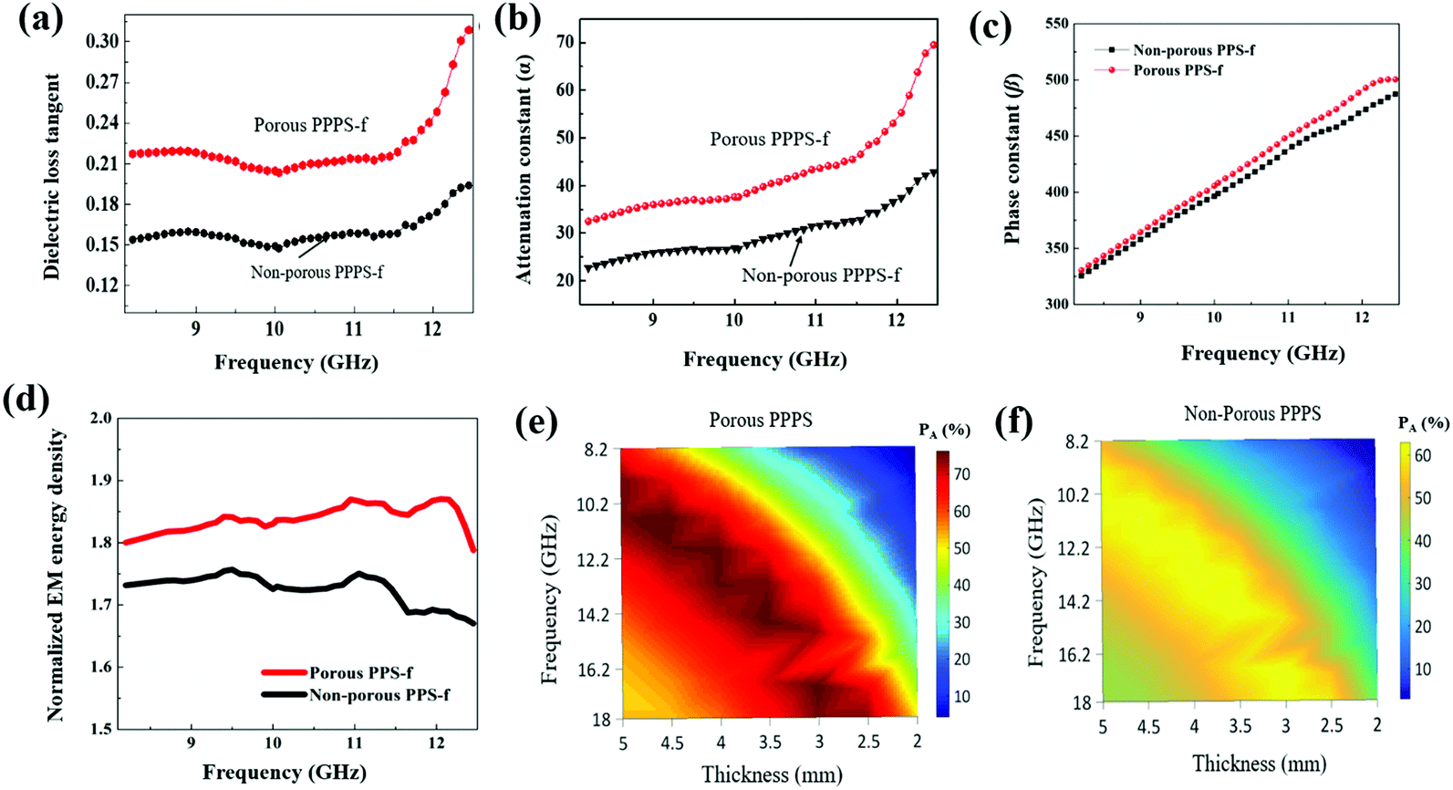

 and
and 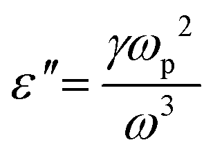 , where ωp parameterizes the interaction strength between the dipole oscillators in the medium and the electric field. The normalized electromagnetic energy density (u) of the porous PPPS-f and non-porous PPPS-f is shown in Fig. 3(d). The normalized u value of the porous PPPS-f is higher than the non-porous PPPS-f. Thus, it indicates the high relative absorption bandwidth of the porous PPPS-f as compared to the non-porous PPPS-f. In order to validate the above discussion, standard EM simulations are carried out using CST-Microwave Studio [4, 6, and 9]. The resulting power levels accepted by both the porous and non-porous PPPS-f are shown in Fig. 3(e) and (f), respectively. The simulation results indicate that the power accepted by the porous PPPS-f is greater than that for the non-porous PPPS-f, especially for the 5 mm thickness.
 , σ is the conductivity).19,20 As shown in Fig. 4(a and b), the Cole–Cole plots show that in the porous PPPS-f semicircles (each semicircle corresponds to dielctric relaxation9,19) are observed. It suggests that εp′′ can not be ignored. Hence energy conversion due to dielectric relaxation is also an important factor in the porous PPPS-f, resulting in better absorption.
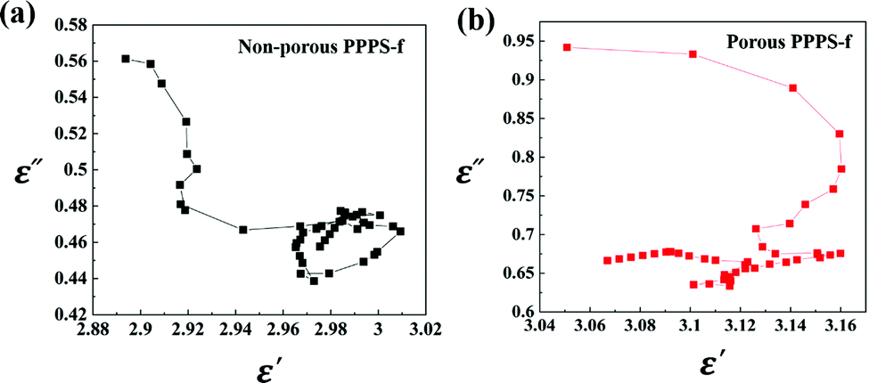
 . Fig. 5(a) and (b) show the obtained A values of the non-porous PPPS-f and porous PPPS-f, respectively. The A value of non-porous PPPS-f was obtained to be 0.1–0.43 (for 1–5 mm thickness, Fig. 5(a)). As shown in Fig. 5(b), for 5 mm thick porous PPPS-f, the A value lies in the range 0.35–0.73. A remarkable improvement of “A” was found in the porous PPPS-f as compared to the non-porous PPPS-f. Thus, it reveals that the microwave absorption characteristics of the porous PPPS-f are much stronger than the non-porous PPPS-f.