
 Open Access Article
 This Open Access Article is licensed under a
 Creative Commons Attribution 3.0 Unported Licence
Enhanced phase transition and infrared photoresponse characteristics in VO2(M1) thin films synthesized by DC reactive sputtering on different substrates
Inyalot Jude
Tadeo
 *,
Saluru B.
Krupanidhi
and
Arun M.
Umarji
*,
Saluru B.
Krupanidhi
and
Arun M.
Umarji
Materials Research Centre, Indian Institute of Science, Bengaluru, 560012, Karnataka, India. E-mail: inyalottadeo@iisc.ac.in
First published on 14th April 2021
Abstract
VO2 is a material with high potential for low-cost optoelectronic, switching and energy saving devices. This work presents the synthesis of smooth high-quality VO2(M1) thin films on quartz (VO2-Qu) and c-sapphire (VO2-Saph) substrates by two-step DC reactive sputtering with enhanced semiconductor-to-metal transition (SMT) and infrared (IR) photoresponse characteristics. Phase formation and purity were confirmed by XRD and Raman measurements. Morphological analysis by AFM and SEM revealed the nanosized nature of the films with a surface roughness of 37 ± 0.5 nm and 48 ± 1 nm for VO2-Qu and VO2-Saph thin films respectively. The VO2-Qu and VO2-Saph thin films exhibit thermally activated SMT temperature (TSMT) of 71 °C and 68 °C with resistance change of 4 and 5 orders of magnitude respectively. Infrared (λ = 1064 nm and 1550 nm) photoresponse characteristics of the low-cost photodetector fabricated based on the synthesized VO2(M1) films increase with a decrease in film roughness. The responsivity increases in the order VO2-Qu (14.02 mA W−1) > VO2-Saph (11.12 mA W−1) under an IR (λ = 1064 nm, 250 mW cm−2) laser at a bias voltage of 10 V. The higher energy (λ = 1064 nm) laser yields an enhanced photoresponse compared to the lower energy (λ = 1550 nm) laser owing to the efficient generation of charge carriers with a higher laser energy. This work provides a way for the large-scale synthesis of high-quality VO2(M1) thin films for various device applications.
1. Introduction
Vanadium dioxide (VO2) is a narrow bandgap (0.6–1.0 eV) n-type phase change material1–6 and is widely studied due to its ability to undergo reversible 1st order semiconductor to metal transition at ∼68 °C, usually accompanied by a drastic resistance change of 3–5 orders of magnitude.3,7–10 This is followed by a change in its optical, transport, magnetic and electrical properties.11,12 These exciting properties make VO2 an appealing material for application in many switching devices like smart windows,13–15 field-effect transistors (FETs),11,16 micro-bolometers,17 thermal rectifiers18 and actuators19 due to the extremely fast switching time, as little as 100 femtoseconds.20,21 In technological advancement, phase change materials22–24 and photodetectors play a key role in several optoelectronic devices as they facilitate the conversion of light of different wavelengths into electric signals. IR photodetectors are of great importance to many sectors ranging from civilian to military.25 Photodetectors have large market value emanating from their numerous applications, including remote sensing, thermography, high-resolution imaging, environmental monitoring, astronomy, industrial processing control, scientific research, military, security checks, night vision cameras, light-wave communication and optoelectronic circuits.25–27 To develop high quality optical and electronic thin film devices based on VO2, the phase must be stabilized, surface roughness should be reduced, and a jump in resistance of at least 3 orders of magnitude must be attained in the films. Monoclinic (M1) VO2 thin films synthesized by numerous single-step and two-step techniques like chemical vapor deposition,28 DC reactive sputtering29 and ultrasonic nebulized spray pyrolysis of aqueous combustion mixtures30 have been shown as low-cost infrared photodetectors. However, the roughness and infrared photoresponse performance of the thin films vary with the substrate's nature and the deposition technique.28–31 Thus, it is vital to understand the crystallization behavior and infrared photoresponse characteristics of VO2(M1) thin films synthesized on different substrates to elucidate the phase formation to improve the quality of films for various device applications. Numerous other techniques like pulsed laser deposition,32 sol–gel,33 atomic layer deposition,34 atmospheric pressure chemical vapor deposition,35 spray pyrolysis,36–38 spin-coating,39 metal–organic chemical vapor deposition,40 molecular beam epitaxy,41 and hydrothermal42 and electron beam evaporation43 have been used to synthesize thin films of VO2 exhibiting a resistance change of 3–5 orders of magnitude on different substrates for various applications. Most switching applications require functional SMT materials like VO2 that show a large resistance drop, sharp hysteresis loop and large transition contrast.44,45 However, phase inhomogeneity and interfacial mismatch between the substrate and the active material greatly hinder their application by rendering reduced transition strength, large hysteresis and low transition contrast, which are profoundly shown to be dependent on the substrate and other thin film deposition parameters.45 Of late, an enormous amount of research has been geared towards improving the crystallinity and stoichiometry of functional materials where the thin film deposition parameters like temperature, pressure and substrate nature are investigated.6,45 The choice of substrate depends on cost and target application. For instance, Si-based substrates like Si(100), PtSi, p-Si and n-Si are employed in FET based industries while non-Si substrates like glass, quartz, and sapphire are used in thermal and optical devices.2,3,46,47 The sapphire substrate is known to yield polycrystalline VO2 films exhibiting a change in resistance of 4–5 orders of magnitude.2,46,47 Thus, a thorough understanding of the effect of the substrate is greatly desired for effective use of VO2 thin films in various devices.Herein, smooth, high-quality VO2(M1) films were synthesized on quartz and c-sapphire substrates by two-step DC reactive sputtering. DC reactive sputtering is a robust technique that yields large-area high-quality, smooth thin films on a large-scale with specific stoichiometry for several device applications.29,48,49 The choice of substrates was based on their structural and physical properties. Quartz is an amorphous substrate and has low thermal conductivity which is particularly useful for high temperature applications. Sapphire has high thermal conductivity which allows quick switching of the deposited films, which is useful for pixel-based applications.2,46,47 Also, the transparent nature of quartz and sapphire substrates makes them useful in various optical industries. The two-step synthesis technique was employed due to the challenges in the synthesis of single-phase VO2 thin films29,31 coupled with the effectiveness of our well established reduction technique reported elsewhere,50 in yielding high-quality VO2(M1) thin films. The influence of the substrate on the SMT and IR photoresponse properties of the synthesized VO2(M1) thin films was investigated where it had a profound effect on the structure, SMT and IR photoresponse characteristics of the films.
2. Experimental
2.1. Synthesis
The VO2(M1) thin films were achieved in a two-step process. In the first step, V2O5 thin films were synthesized on quartz and c-sapphire substrates by a DC reactive sputtering (Hydro Pneo Vac Technologies) unit using deposition conditions specified in Table 1. All the substrates were placed on the heater plate at the same time and equilibrated for 30 minutes to ensure uniform deposition temperature. It is assumed that the temperature measured at the heater base plate is in equilibrium with surface temperatures of the different substrates. The base chamber pressure was attained before commencing the deposition process. The working pressure was kept constant throughout the deposition time. Reactant gases consisting of oxygen and argon were maintained at a flow rate of 0.05 and 5 sccm respectively, using MKS mass flow controllers. Pre-sputtering was done for 15 minutes to remove any contamination on the target material before the deposition of thin films commenced, which was performed in a 0.095 m3 chamber at a substrate temperature of 450 °C for 45 minutes. This gave phase pure V2O5 thin films.| Parameter | Value |
|---|---|
| Target | V metal (2′′ × 0.25′′, 99.99% pure) |
| Substrate | Quartz and c-sapphire |
| Distance between the target and substrate | 10 cm |
| Base chamber pressure | 5.3 × 10⁻⁵ mbar |
| Working pressure | 8.1 × 10⁻³ mbar |
| Power | 200 W |
| Argon flow rate | 5 sccm |
| Oxygen flow rate | 0.05 sccm |
| Deposition temperature | 450 °C |
| Duration of deposition | 45 minutes |
The second step involved a controlled reduction of synthesized V2O5 films to give VO2(M1) films using our well established reduction technique.50 A schematic diagram of the in-house built reduction setup is given in Fig. 1. Briefly, the sample is placed in a quartz tube with one of its ends closed and kept in a tubular furnace. The other end of the tube is attached to a specially designed coupler which is used to connect it to a bubbler containing a hydrocarbon like n-hexane, benzene or toluene. The bubbler is in turn connected to a nitrogen gas cylinder through the mass flow controller (MKS Instruments, USA) which is used to control the flow rate as the gas saturates with the hydrocarbon. N2 gas, saturated with the hydrocarbon, was continuously flowed into the furnace at a rate of 45 sccm. The as synthesized V2O5 thin films were kept in the reduction chamber at 550 °C for 2 hours and then cooled to room temperature giving phase pure VO2 thin films.
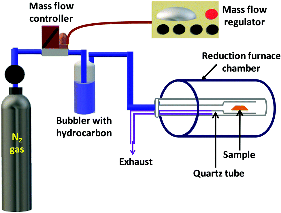 | ||
| Fig. 1 Schematic diagram of the in-house built setup used to reduce V2O5 thin films into VO2 thin films. | ||
The V–O phase diagram,8,51 specifically the correlation between the partial pressure of oxygen, temperature and the phase stability were used to deduce optimum conditions for reduction so that single phase VO2 would result. The synthesized thin films were represented by sample codes as given in Table 2.
| Sample code (V2O5 based) | Sample code (VO2 based) | Substrate |
|---|---|---|
| V2O5-Qu | VO2-Qu | Quartz |
| V2O5-Saph | VO2-Saph | c-Sapphire |
2.2. Characterization
Phase purity was analyzed from X-ray diffraction measurements carried out using a PANalytical instrument with Cu Kα radiation (1.5418 Å) at a scan rate of 2° min−1. Phase formation and its purity were confirmed from Raman measurements recorded using the Horiba JobinYvon HR-Raman-123 microPL spectrometer at a wavelength of 532 nm. The thin film morphology was investigated using a non-contact mode A.P.E. Research A100-AFM atomic force microscope and an Inspect F50 field emission scanning electron microscope. The Veeco Dektak 6M surface profilometer was used to measure the thickness of thin films. SMT characteristics of VO2(M1) thin films were studied from electrical measurements performed using a DC electrical probe station equipped with the ATT thermal controller and coupled with a B1500A semiconductor device analyzer.2.3. Fabrication of a photodetector device
The IR photodetector devices used for the photodetection studies were fabricated by depositing electrical contacts comprising of Cr (6 nm)/Au (80 nm) and measuring 1 mm × 1 mm in width and length on top of the synthesized VO2 thin films by thermal evaporation aided by a mask. The photoresponse properties of devices were recorded using a Keithley SMU2400 source meter. A CNI MDL-III 1550 nm laser with an optical coupler of ∼2 mm and an MIL-III 1064 nm laser (beam radius of 2.5 mm) were used as the infrared source.3. Results and discussion
3.1. Structural characterization: XRD studies
Fig. 2a presents the XRD patterns of V2O5-Qu and V2O5-Saph thin films deposited by DC reactive sputtering. The synthesized V2O5-Qu and V2O5-Saph thin films were then reduced to give VO2-Qu and VO2-Saph thin films respectively, whose phase formation and purity were confirmed from their XRD patterns shown in Fig. 2b.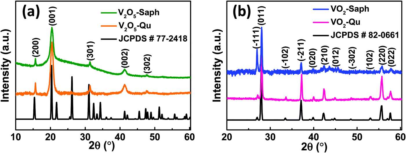 | ||
| Fig. 2 XRD patterns of (a) V2O5-Qu and V2O5-Saph thin films; and (b) VO2-Qu and VO2-Saph thin films deposited by DC reactive sputtering. | ||
All thin films deposited were phase pure as no impurity peak of other vanadium oxides was detected. The V2O5 was indexed to the Pmmn space group of the orthorhombic crystal system (JCPDS #77-2418),52,53 and VO2 was indexed to the monoclinic (M1) phase of VO2 with the space group P21/c (JCPDS #82-0661).28–31,54 Achieving the right conditions for thin film deposition and reduction, most especially temperature, oxygen partial pressure and using a nitrogen atmosphere saturated with hydrocarbons to yield the desired VO2(M1) films is one of the greatest accomplishments of this study.
3.2. Raman spectroscopy studies
The phase formation and purity of the synthesized VO2(M1) thin films were further confirmed from room temperature Raman measurements. Fig. 3a shows the room temperature Raman spectra of V2O5-Qu and V2O5-Saph thin films deposited by DC reactive sputtering. All the V2O5-Qu and V2O5-Saph thin films featured 10 Raman peaks at peak positions matching those reported for crystalline V2O5.53,55–59 The Raman peaks observed were assigned to various bending and stretching vibrational modes of V2O5 as 102(Ag), 145(B2g, B3g), 197(B1g), 283(B3g, B2g), 304(Ag), 404(Ag), 487(Ag), 528(Ag), 703(B3g, B2g) and 995(Ag) cm−1.53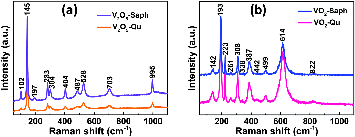 | ||
| Fig. 3 Room temperature Raman spectra of (a) V2O5-Qu and V2O5-Saph thin films; and (b) VO2-Qu and VO2-Saph thin films deposited by DC reactive sputtering. | ||
Fig. 3b shows the Raman spectra, taken at room temperature, for VO2-Qu and VO2-Saph thin films synthesized by two-step DC reactive sputtering. The Raman spectra of VO2-Qu and VO2-Saph thin films showed 11 distinct peaks corresponding to monoclinic (M1) VO216,28–31,60,61 further proving the phase purity of the synthesized thin films. The peaks were observed at positions 142, 193, 223, 261, 308, 338, 387, 442, 499, 614 and 822 cm−1 and were assigned to the phonon modes B1g, Ag, Ag, Ag, Ag, Ag, Ag, Eg, Ag, Ag and B2g respectively, of VO2(M1).16,62
3.3. Morphological analysis
The surface morphology of the deposited VO2(M1) thin films was investigated using AFM and SEM. Fig. 4 shows 3D AFM images of VO2-Qu and VO2-Saph thin films deposited by two-step DC reactive sputtering. They clearly show the smooth nature of the thin films having well-grown and uniform grains. The VO2-Qu and VO2-Saph thin films deposited by two-step DC reactive sputtering had relatively low surface roughness of 37 ± 0.5 and 48 ± 1 nm respectively, justifying their suitability for use in several optical devices as they scatter light to a lesser extent.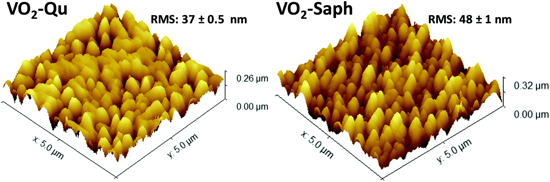 | ||
| Fig. 4 3D AFM images of VO2-Qu and VO2-Saph thin films synthesized by two-step DC reactive sputtering. | ||
The thickness of the deposited VO2(M1) thin films was 150–160 nm from Veeco Dektak 6M surface profilometer measurements.
Fig. 5 shows SEM images of VO2-Qu and VO2-Saph thin films synthesized by two-step DC reactive sputtering. They clearly show the well-grown grains, packed and continuous, suitable for application in various optoelectronic and switching devices. The substrate effect is visible on the shape, size and compactness of grains, with VO2-Saph thin films showing the most compact and largest particle size. The average particle size, determined using Image-J software63 was 155 ± 7 nm and 260 ± 4 nm for VO2-Qu and VO2-Saph thin films respectively.
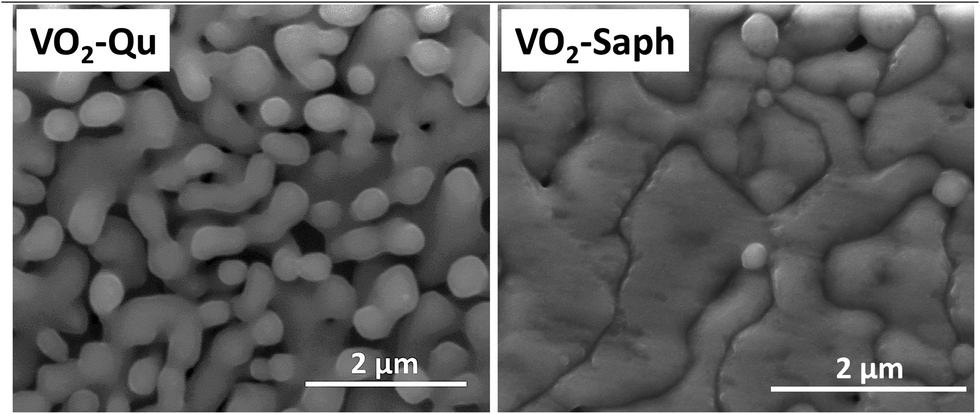 | ||
| Fig. 5 SEM images of VO2-Qu and VO2-Saph thin films deposited by two-step DC reactive sputtering. | ||
3.4. Electrical studies
The electrical properties were analysed from I–V measurements recorded on VO2-Qu and VO2-Saph thin films as a function of temperature (25 °C to 110 °C). The resistance (R) obtained from the slope of voltage versus the current plot was then plotted against temperature. Fig. 6(a and c) show plots of normalized resistance (R(T)/R(RT)) versus temperature for VO2-Qu and VO2-Saph thin films respectively. The dependence of resistivity of VO2 thin films on the temperature is an indication of SMT and the magnitude of resistance change shows the quality of the thin films. The VO2-Qu and VO2-Saph thin films exhibited an abrupt first-order SMT with a change in resistance of 4 and 5 orders of magnitude respectively. The highest resistance change (5 orders of magnitude switching) exhibited by VO2-Saph thin films is comparable to that shown by single crystals64 of VO2 and it indicates complete growth of thin films with good connectivity.2,47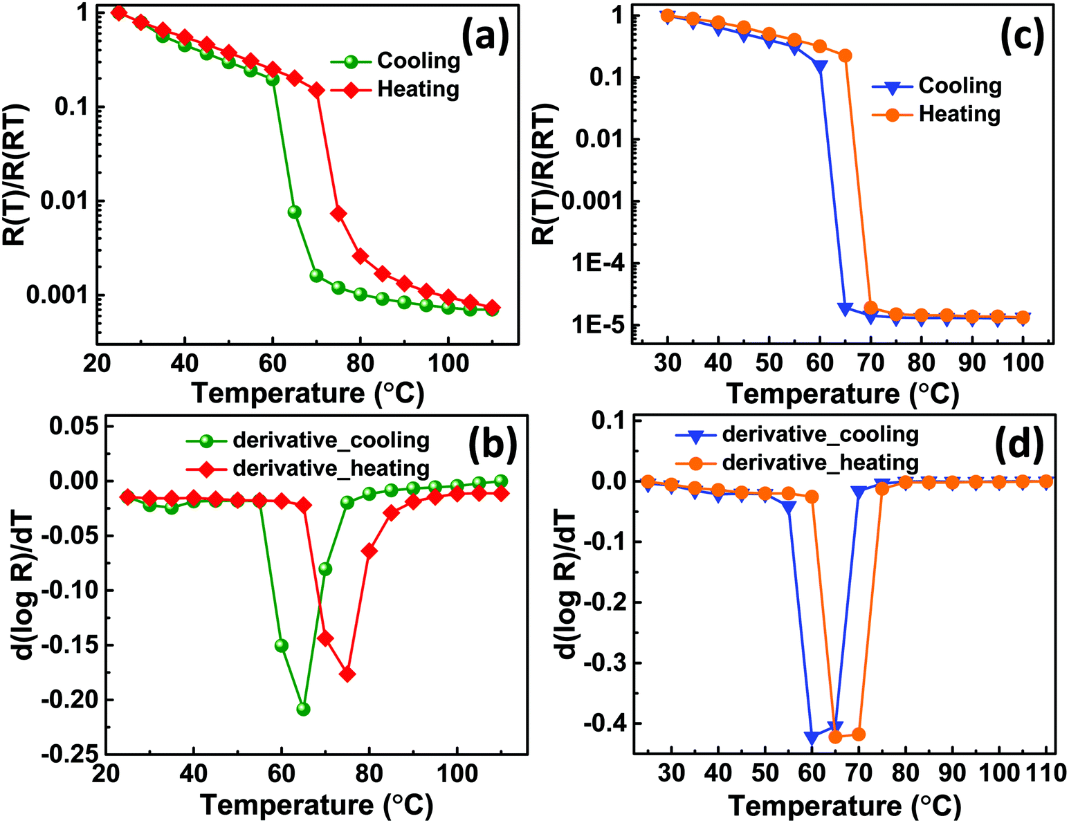 | ||
Fig. 6 (a and c) Normalized resistance as a function of temperature plots for VO2-Qu and VO2-Saph thin films respectively; (b and d) heating and cooling derivative d(log![[thin space (1/6-em)]](https://www.rsc.org/images/entities/char_2009.gif) R)/dT plots for VO2-Qu and VO2-Saph thin films respectively, deposited by two-step DC reactive sputtering. R)/dT plots for VO2-Qu and VO2-Saph thin films respectively, deposited by two-step DC reactive sputtering. | ||
Fig. 6(b and d) show the derivative plots for VO2-Qu and VO2-Saph thin films from which the SMT temperatures (TSMT) were obtained. The TSMT was observed not to happen at a single temperature as different peaks were identified during heating and cooling cycles. The VO2-Qu and VO2-Saph thin films exhibited thermally activated TSMT of 71 °C and 68 °C, respectively, which was in agreement with other reports.3,10,47 The resistance ratio (ΔA), expressed as  indicates the strength of the transition where R(T1), R(T) and R(Tm) denote the resistance at initial/room temperature (T1/RT), any temperature (T), and maximum/final temperature (Tm) respectively. The resistance ratio (ΔA), transition width (ΔT), thermal hysteresis (ΔTh) and the temperature coefficient of resistance (TCR), which measures the change in resistance of a material per degree of temperature change, were determined as given in Table 3.
| Sample | VO2-Qu | VO2-Saph | VO2–Si(100)29 |
|---|---|---|---|
| Surface roughness (nm) | 37 ± 0.5 | 48 ± 1 | 8 ± 0.7 |
| Transition temperature, Tc (°C) | 71 | 68 | 68 |
| Transition width, ΔT (°C) | 9 | 5 | 10 |
| Thermal hysteresis, ΔTh (°C) | 10 | 5 | 10 |
| Resistance ratio, ΔA on heating | 1356 | 75187 |
164 |
| Resistance ratio, ΔA on cooling | 1425 | 75216 |
181 |
| TCR at 30 °C (% K−1) on heating | −1.25 | −1.25 | −1.24 |
| TCR at 30 °C (% K−1) on cooling | −1.25 | −1.25 | −1.24 |
| E a (± error) (meV) on heating | 364 ± 11 | 336 ± 22 | 228 ± 12 |
| 318 ± 3 | 48 ± 6 | 198 ± 16 | |
| E a (± error) (meV) on cooling | 128 ± 15 | 21 ± 11 | 119 ± 7 |
| 370 ± 4 | 399 ± 10 | 361 ± 56 |
The VO2-Saph thin films exhibited the highest switching ratio and the lowest hysteresis width, which are desirable for fabricating high-quality devices used for various switching applications. It's clear from Table 3 that the synthesized VO2-Qu and VO2-Saph thin films exhibit better SMT characteristics than VO2(M1) films deposited on Si(100) substrate by the same deposition technique.29 The high values of resistance ratio shown by all thin films are attributed to the complete formation of the monoclinic (M1) phase of VO2 with no other phase.28–31 No appreciable change in the TCR values was observed for all the films; the recorded values were consistent with the literature reports.65,66 The activation energies, Ea of VO2-Qu and VO2-Saph thin films were determined from the relation R(T) = R0eEa/kBT where Ea is the slope of lnR(T) versus 1/kBT plot.29–31 The activation energies of the deposited VO2(M1) thin films were determined for both heating and cooling curves as shown in Fig. 7. The VO2-Saph thin films showed the highest (5 orders of magnitude) change in resistance and exhibited the lowest activation energies in the high-temperature phase.
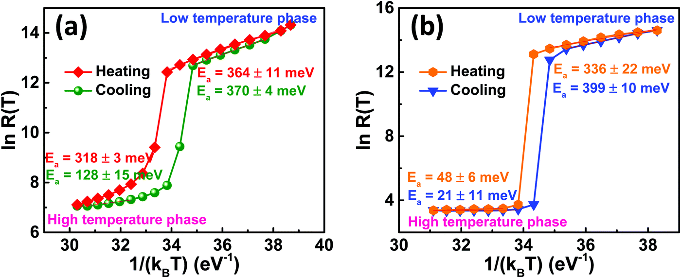 | ||
| Fig. 7 Activation energy studies from lnR(T) against 1/kBT plot during heating and cooling cycles for (a) VO2-Qu and (b) VO2-Saph thin films synthesized by two-step DC reactive sputtering. | ||
Also, it has the maximum change in Ea on switching, indicating that the high-temperature phase is almost entirely metallic with a sapphire substrate. VO2 in the ‘metallic’ phase is considered a ‘poor metal’.67–69 Also, the ‘metallic’ phase might not be ideally metallic because of the presence of defects due to the deposition technique and conditions.69
3.5. Photodetection studies
The photoresponse characteristics of the fabricated photodetector devices based on the synthesized VO2(M1) thin films were investigated by shining an infrared laser (λ = 1064 nm and 1550 nm) under different power densities at room temperature. The schematic diagram of the fabricated device is presented in Fig. 8a. Fig. 8b shows room temperature I–V curves in the dark and on illuminating with a 1064 nm laser at different intensities for photodetector fabricated based on VO2-Qu thin films. The curves were linear, signifying the ohmic nature of contacts. VO2-Saph thin films exhibited similar I–V curves.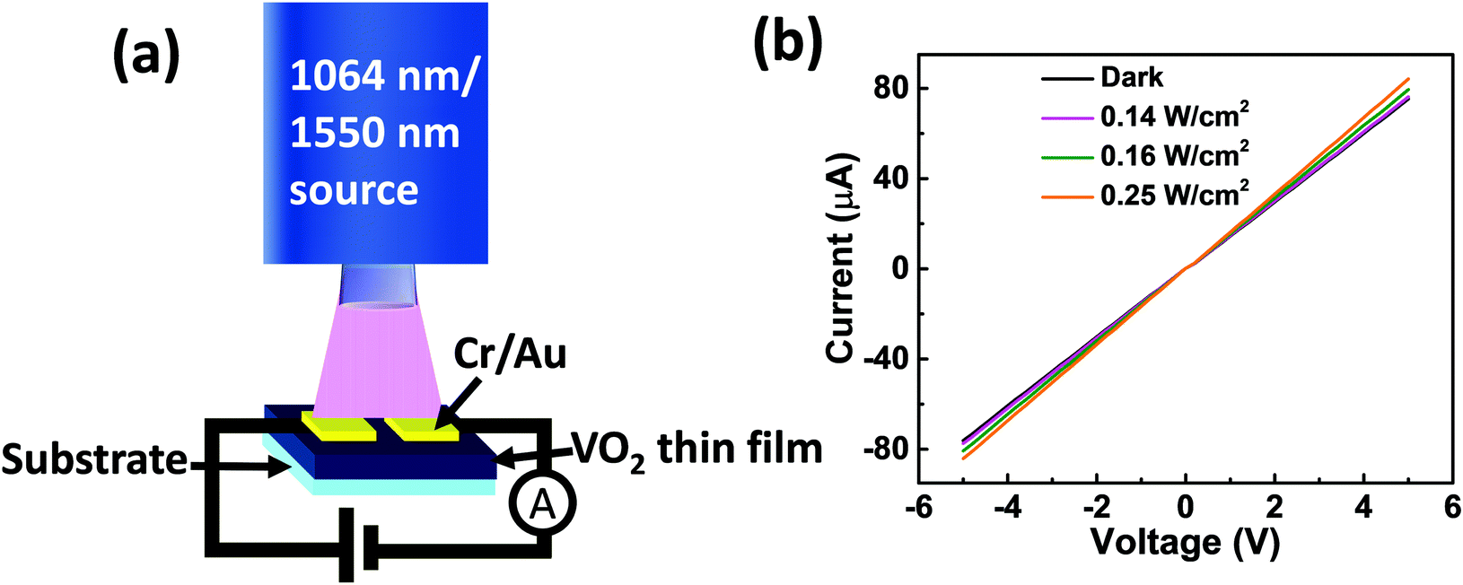 | ||
| Fig. 8 (a) Device schematic and (b) I–V curves for the device fabricated based on VO2-Qu thin films in the dark and on illuminating with infrared (1064 nm) laser at different power densities. | ||
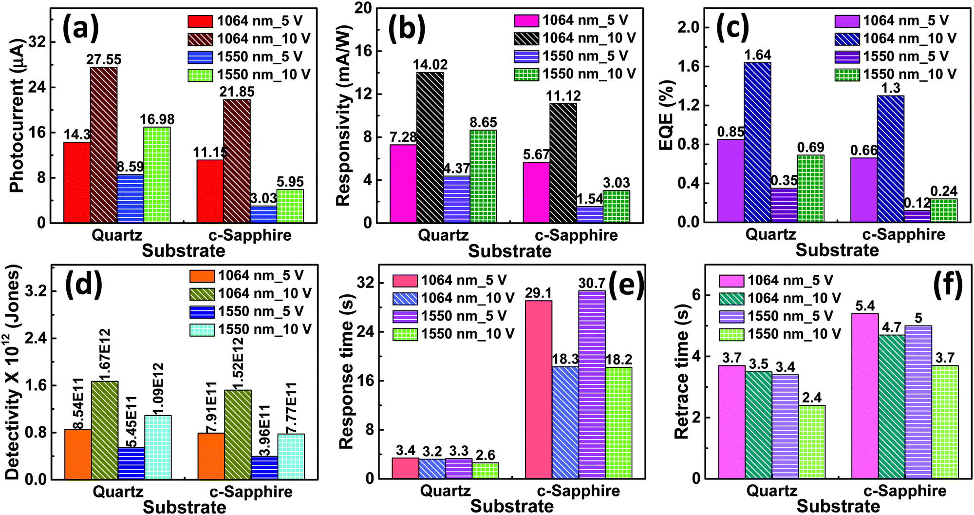
Fig. 9(a–d) shows the change in photocurrent with respect to time for the photodetector fabricated based on (a and b) VO2-Qu and (c and d) VO2-Saph thin films upon illumination with (a and c) 1064 nm laser and (b and d) 1550 nm laser under constant power density of 250 mW cm−2 at a bias voltage of 5 V and 10 V. The photoresponse increased with the increase in bias voltage, an observation consistent with the power law.70
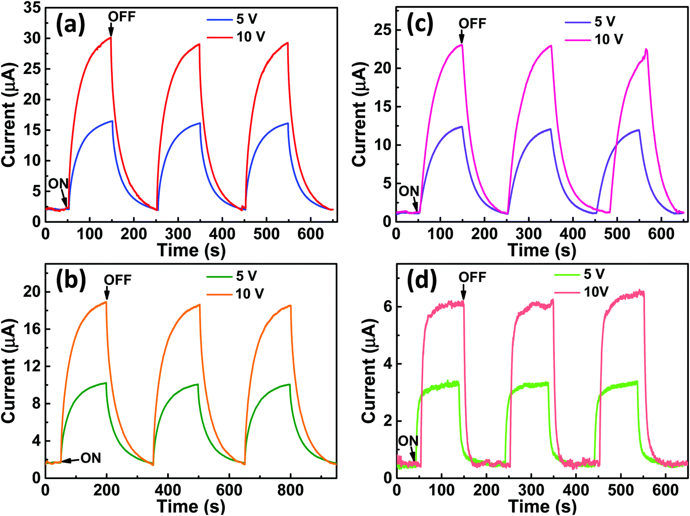 | ||
| Fig. 9 ON and OFF photoresponse characteristics of the fabricated device based on (a and b) VO2-Qu and (c and d) VO2-Saph thin films deposited by two-step DC reactive sputtering upon illumination with a (a and c) 1064 nm laser and (b and d) 1550 nm laser under constant power density of 250 mW cm−2 at 5 V and 10 V bias voltage. | ||
The increase in photocurrent is attributed to the efficient separation of charge carriers with fewer trap states and interaction between photogenerated carriers at higher bias. At lower bias trap states, the interactions between the photogenerated carriers (electron–hole pairs) are involved in the recombination kinetics of photocarriers which leads to a low photocurrent.70,71 The photoresponse was repeated for many cycles but only a few cycles are given to avoid clutter. The photocurrent, given in Fig. 10a, was observed to increase with a reduction in the thin film surface roughness under both cases of laser energies. The photocurrent increased in the order: VO2-Qu (8.59–27.55 μA) > VO2-Saph (3.03–21.85 μA) while the surface roughness varied as VO2-Qu (RMS: 37 ± 0.5 nm) < VO2-Saph (RMS: 48 ± 1 nm). This trend in photoresponse exhibited by the synthesized thin films can be ascribed to the effect of light scattering, which reduces with a reduction in the surface roughness of thin films. The responsivity indicates how the efficiency of a detector responds to the optical signal.72Rλ is defined as photocurrent realized per unit power of incident light on the effective area of the device and expressed as 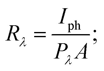 where Iph is photocurrent Iph = Ilight − Idark, Pλ is power density and A is the effective area of the device.71,72 EQE is a ratio of the number of electron–hole pairs (ne) with a contribution to the photocurrent to the total number of incident photons (nphotons). It is defined as a measure of the number of photons absorbed to the number of incident photons and expressed as
 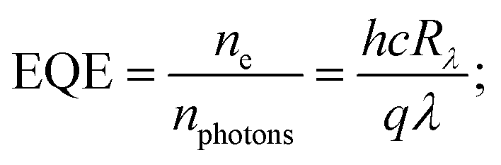 where h is Planck's constant, c is the speed of light, q is the electron charge and λ is the wavelength of the laser used.70,71 Detectivity determines the sensibility of a device to detect weak optical signals and is calculated from the relation
 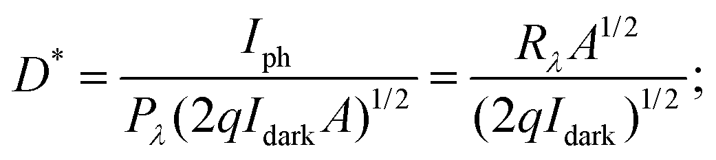 where A, the effective area of detector, is in cm2.71,73 A high detectivity indicates a better performance of the photodetector.
 | ||
| Fig. 10 Comparison of photoresponse properties of the photodetector fabricated based on VO2-Qu and VO2-Saph thin films synthesized by two-step DC reactive sputtering under illumination with IR (λ = 1064 nm and 1550 nm) laser in a constant power density of 250 mW cm−2 at a bias voltage of 5 V and 10 V; (a) photocurrent, (b) responsivity, (c) EQE, (d) detectivity, (e) response time and (f) retrace time. | ||
Fig. 10(b–f) show responsivity, quantum efficiency, detectivity, response time and retrace time respectively, of the photodetector fabricated based on VO2-Qu and VO2-Saph thin films upon illumination with an IR (λ = 1064 nm and 1550 nm) laser with a power density of 250 mW cm−2 at 5 V and 10 V bias. In all thin films, the infrared photoresponse of the photodetector decreased with an increase in the surface roughness of the thin films, which can be ascribed to the effect of increased light scattering arising from the increased surface roughness of the thin films.74 The performance of our photodetector devices are compared with previously reported infrared photodetector devices in Table 4.28,30,70,71,75 The responsivity and the detectivity exhibited by our devices at both laser energies (λ = 1064 nm and 1550 nm) are better than those reported.28,30,70,71,75
| IR photodetector | R λ (mA W−1) at λ (nm) | D* (jones) at λ (nm) | τ resp (s) | τ retr (s) | ||
|---|---|---|---|---|---|---|
| 1064 | 1550 | 1064 | 1550 | |||
| R λ is responsivity, D* is detectivity, τresp is response time and τretr is retrace time. | ||||||
| VO2(M1) thin films30 | 1.54 | 3.53 × 10¹⁰ | 1.17 | 1.08 | ||
| SnS2 thin films71 | 1.8 | 1011 | 2.5 | 3.68 | ||
| WS2 monolayer70 | 6.6 | 0.004 | 0.005 | |||
| VO2(M1) thin films28 | 7.13 × 10⁻² | 1.06 × 10¹¹ | 2.23 | 3.67 | ||
| VO2(M1) thin films29 | 40.1 | 3.0 × 10¹² | 0.1–0.14 | 0.1–1.2 | ||
| P3HT–PCBM polymer75 | 3.01 | 7.97 × 10⁸ | 4.9 | 6.3 | ||
| This work | ||||||
| VO2-Qu thin films | 14.02 | 8.65 | 1.67 × 10¹² | 1.09 × 10¹² | 2.5–3.2 | 2.4–3.5 |
| VO2-Saph thin films | 11.12 | 3.03 | 1.52 × 10¹² | 7.77 × 10¹¹ | 18.2–18.3 | 3.7–4.7 |
The dynamic response of the fabricated device to IR source can be described by exponential equations I(t)growth = Idark + αet/τ1 + βet/τ2 and I(t)decay = Idark + χe−t/τ1 + γe−t/τ2 for growth and decay respectively,71,76,77 where t is time for ON or OFF cycles; Idark is dark current, τ1 and τ2 are time constants; α, β, χ and γ are the scaling constants. The response and the retrace time were determined from the solutions to those 2nd order exponential equations by fitting one cycle of each of the growth and decay response curves, at 5 V and 10 V. The average response time constants were then computed from the relation 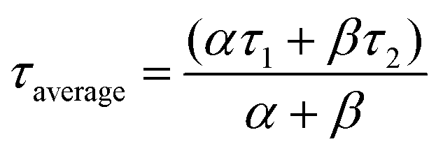 .71 The response time and retrace time exhibited by our devices were comparable to those reported. The mechanism of photodetection is based on the principle of the photovoltaic effect. It involves the generation of excess free electron–hole pairs (charge carriers) by a material absorbing photons with photon energy greater than the material's bandgap which leads to a reduction in its electrical resistance.78 Before the application of bias, charge carriers present in VO2(M1) thin films are free. On application of an external bias, the barrier is overcome, charge carriers go to respective electrodes contributing to the dark current and the metal-semiconductor interface gets depleted of charge carriers. On illuminating the photodetector device fabricated based on the synthesized VO2(M1) thin films with the photon energy of λ = 1064 nm or 1550 nm ∼1.16 eV or 0.8 eV respectively, which is greater than the bandgap of VO2 (0.6–0.7 eV),3,79 the VO2(M1) thin film absorbs the radiation, charge carriers (excitons) are generated and separated by applied bias. These carriers collect at the electrodes and add to the available dark current making up the recorded photocurrent.78 To rule out the substrate's contribution to the photocurrent, photodetection measurements were done on bare quartz and c-sapphire substrates. No appreciable photocurrent was recorded on the bare substrates suggesting that the VO2(M1) thin films entirely account for the observed photocurrent.
4. Conclusions
Smooth phase pure VO2(M1) thin films could be deposited on quartz and c-sapphire substrates by two-step DC reactive sputtering. Phase formation and purity were confirmed by XRD and Raman measurements. Morphological analysis by AFM and SEM revealed the nanosized nature of VO2(M1) thin films with a surface roughness of 37 ± 0.5 nm and 48 ± 1 nm for VO2-Qu and VO2-Saph thin films respectively, which is smooth enough for various device applications. SMT studies showed an abrupt 1st order transition of the thin films across the transition temperature of 68 °C with a resistance change of 4 and 5 orders of magnitude for VO2-Qu and VO2-Saph thin films respectively which was higher than that reported for VO2(M1) films deposited on a Si(100) substrate29 by the same technique. The low-cost infrared photodetectors fabricated based on the synthesized VO2(M1) thin films exhibited high IR (λ = 1064 nm and 1550 nm) photoresponse properties. The IR photoresponse of the fabricated devices was dependent on the surface roughness of thin films. Responsivity increased in the order VO2-Qu (14.02 mA W−1) > VO2-Saph (11.12 mA W−1) under an IR (λ = 1064 nm, 250 mW cm−2) laser at a bias voltage of 10 V. An enhanced photoresponse (responsivity of 11.12–14.02 mA W−1 and a detectivity of 1.52 × 10¹²–1.67 × 10¹² jones) was realized with a higher energy (λ = 1064 nm) laser as compared to a lower energy (λ = 1550 nm) laser (responsivity of 3.03–8.65 mA W−1 and detectivity of 7.77 × 10¹¹–1.09 × 10¹² jones) attributed to efficient generation of charge carriers at higher laser energy. These results show the suitability of the synthesis technique employed and the substrate choice to prepare VO2(M1) thin films for different applications in optoelectronic and switching devices.Author contributions
All the authors contributed to the writing of the manuscript. Inyalot Jude Tadeo: (first and corresponding author) carrying out experiments, formal analysis, manuscript writing, review and editing. Saluru B. Krupanidhi: conceptualization, supervision, review and editing. Arun M. Umarji: conceptualization, supervision, formal analysis, review and editing.Conflicts of interest
There are no conflicts to declare.Acknowledgements
Authors acknowledge the Indian Institute of Science, Bengaluru, India, through the Micro and Nano Characterization Facility at the Centre for Nano Science and Engineering (CeNSE) for providing characterization facilities. Prof. Karuna Kar Nanda is acknowledged for his technical insights. Inyalot Jude Tadeo greatly thanks the Indian Institute of Science, Bengaluru, through the Office of International Relations for granting him his PhD fellowship.References
- W. Li, S. Ji, K. Qian and P. Jin, J. Colloid Interface Sci., 2015, 456, 166–173 CrossRef CAS PubMed.
- D. Ruzmetov, K. T. Zawilski, S. D. Senanayake, V. Narayanamurti and S. Ramanathan, J. Phys.: Condens. Matter, 2008, 20, 465204 CrossRef PubMed.
- Z. Yang, C. Ko and S. Ramanathan, Annu. Rev. Mater. Res., 2011, 41, 337–367 CrossRef CAS.
- C. N. Berglund and H. J. Guggenheim, Phys. Rev., 1969, 185, 1022–1033 CrossRef CAS.
- W. W. Li, J. J. Zhu, X. F. Xu, K. Jiang, Z. G. Hu, M. Zhu and J. H. Chu, J. Appl. Phys., 2011, 110, 1–6 Search PubMed.
- D. P. Zhang, M. D. Zhu, Y. Liu, K. Yang, G. X. Liang, Z. H. Zheng, X. M. Cai and P. Fan, J. Alloys Compd., 2016, 659, 198–202 CrossRef CAS.
- C. Wu, F. Feng and Y. Xie, Chem. Soc. Rev., 2013, 42, 5157–5183 RSC.
- J. Nag and R. F. Haglund, J. Phys.: Condens. Matter, 2008, 20, 264016 CrossRef.
- Y. Ke, S. Wang, G. Liu, M. Li, T. J. White and Y. Long, Small, 2018, 14, 102025 Search PubMed.
- F. J. Morin, Phys. Rev. Lett., 1959, 3, 34–36 CrossRef CAS.
- D. Ruzmetov, D. Heiman, B. B. Claflin, V. Narayanamurti and S. Ramanathan, Phys. Rev. B: Condens. Matter Mater. Phys., 2009, 79, 10–13 CrossRef.
- M. Liu, H. Y. Hwang, H. Tao, A. C. Strikwerda, K. Fan, G. R. Keiser, A. J. Sternbach, K. G. West, S. Kittiwatanakul, J. Lu, S. A. Wolf, F. G. Omenetto, X. Zhang, K. A. Nelson and R. D. Averitt, Nature, 2012, 487, 345–348 CrossRef CAS PubMed.
- Z. Zhang, Y. Gao, Z. Chen, J. Du, C. Cao, L. Kang and H. Luo, Langmuir, 2010, 26, 10738–10744 CrossRef CAS PubMed.
- F. Xu, X. Cao, H. Luo and P. Jin, J. Mater. Chem. C, 2018, 6, 1903–1919 RSC.
- Z. Wen, Y. Ke, C. Feng, S. Fang, M. Sun, X. Liu and Y. Long, Adv. Mater. Interfaces, 2020, 2001606 Search PubMed.
- J. M. Wu and L. B. Liou, J. Mater. Chem., 2011, 21, 5499 RSC.
- B. Wang, J. Lai, H. Li, H. Hu and S. Chen, Infrared Phys. Technol., 2013, 57, 8–13 CrossRef CAS.
- C. L. Gomez-Heredia, J. A. Ramirez-Rincon, J. Ordonez-Miranda, O. Ares, J. J. Alvarado-Gil, C. Champeaux, F. Dumas-Bouchiat, Y. Ezzahri and K. Joulain, Sci. Rep., 2018, 8, 1–11 CAS.
- A. Rúa, F. E. Fernández and N. Sepúlveda, J. Appl. Phys., 2010, 107, 1–5 Search PubMed.
- R. M. Briggs, I. M. Pryce and H. A. Atwater, Opt. Express, 2010, 18, 11192–11201 CrossRef CAS PubMed.
- F. E. F. Horacio Coy, R. Cabrera and N. Sepúlveda, J. Appl. Phys., 2010, 108, 113115 CrossRef.
- M. N. Julian, C. Williams, S. Borg, S. Bartram and H. J. Kim, Optica, 2020, 7, 746 CrossRef CAS.
- F. Zhang, X. Xie, M. Pu, Y. Guo, X. Ma, X. Li, J. Luo, Q. He, H. Yu and X. Luo, Adv. Mater., 2020, 32, 1908194 CrossRef CAS PubMed.
- A. K. U. Michel, S. Meyer, N. Essing, N. Lassaline, C. R. Lightner, S. Bisig, D. J. Norris and D. N. Chigrin, Adv. Optical Mater., 2021, 9, 2001243 CrossRef CAS.
- J. Hou, Z. Wang, Z. Ding, Z. Zhang and J. Zhang, Sol. Energy Mater. Sol. Cells, 2018, 176, 142–149 CrossRef CAS.
- S. C. H. Woong Choi, M. Yeon Cho, A. Konar, J. Hak Lee and G.-B. Cha, Adv. Mater., 2012, 24, 5832–5836 CrossRef PubMed.
- Y.-H. Chang, W. Zhang, Y. Zhu, Y. Han, J. Pu, J.-K. Chang, W.-T. Hsu, J.-K. Huang, C.-L. Hsu, M.-H. Chiu, T. Takenobu, H. Li, C.-I. Wu, W.-H. Chang, A. T. S. Wee and L.-J. Li, ACS Nano, 2014, 8, 8582–8590 CrossRef CAS PubMed.
- B. Rajeswaran, I. J. Tadeo and A. M. Umarji, J. Mater. Chem. C, 2020, 8, 12543–12550 RSC.
- I. J. Tadeo, D. Bhardwaj, D. Sheela, S. B. Krupanidhi and A. M. Umarji, J. Mater. Sci.: Mater. Electron., 2020, 31, 4687–4695 CrossRef CAS.
- I. J. Tadeo, E. P. Mukhokosi, S. B. Krupanidhi and A. M. Umarji, RSC Adv., 2019, 9, 9983–9992 RSC.
- I. J. Tadeo, B. Rajeswaran and A. M. Umarji, J. Phys. D: Appl. Phys., 2020, 53, 185104 CrossRef CAS.
- J. Jian, X. Wang, L. Li, M. Fan, W. Zhang, J. Huang, Z. Qi and H. Wang, ACS Appl. Mater. Interfaces, 2017, 9, 5319–5327 CrossRef CAS PubMed.
- Y. Ningyi, L. Jinhua and L. Chenglu, Appl. Surf. Sci., 2002, 191, 176–180 CrossRef.
- F. Mattelaer, K. Geryl, G. Rampelberg, T. Dobbelaere, J. Dendooven and C. Detavernier, RSC Adv., 2016, 6, 114658–114665 RSC.
- C. S. Blackman, C. Piccirillo, R. Binions and I. P. Parkin, Thin Solid Films, 2009, 517, 4565–4570 CrossRef CAS.
- B. W. Mwakikunga, E. Sideras-Haddad and M. Maaza, Opt. Mater., 2007, 29, 481–487 CrossRef CAS.
- M. Benkahoul, M. K. Zayed, A. Solieman and S. N. Alamri, J. Alloys Compd., 2017, 704, 760–768 CrossRef CAS.
- M. M. Margoni, S. Mathuri, K. Ramamurthi, R. R. Babu and K. Sethuraman, Thin Solid Films, 2016, 606, 51–56 CrossRef CAS.
- M. Li, S. Ji, J. Pan, H. Wu, L. Zhong, Q. Wang, F. Li and G. Li, J. Mater. Chem. A, 2014, 2, 20470–20473 RSC.
- M. B. Sahana, G. N. Subbanna and S. A. Shivashankar, J. Appl. Phys., 2002, 92, 6495–6504 CrossRef CAS.
- P. Schiffer, D. G. Schlom, J. W. Tashman, J. H. Lee, H. Paik, J. A. Moyer, R. Misra, J. A. Mundy and T. Spila, Appl. Phys. Lett., 2015, 063104 Search PubMed.
- J. Zhang, J. Li, P. Chen, F. Rehman, Y. Jiang, M. Cao, Y. Zhao and H. Jin, Sci. Rep., 2016, 6, 27898 CrossRef CAS PubMed.
- F. Ureña-Begara, A. Crunteanu and J. P. Raskin, Appl. Surf. Sci., 2017, 403, 717–727 CrossRef.
- C. Zhang, C. Koughia, Y. Li, X. Cui, F. Ye, S. Shiri, M. Sanayei, S. J. Wen, Q. Yang and S. Kasap, Appl. Surf. Sci., 2018, 440, 415–420 CrossRef CAS.
- C. Zhang, C. Koughia, O. Güneş, J. Luo, N. Hossain, Y. Li, X. Cui, S. J. Wen, R. Wong, Q. Yang and S. Kasap, J. Alloys Compd., 2020, 848, 1–13 CrossRef.
- S. Ramanathan, Thin Film Metal-Oxides: Fundamentals and Applications in Electronics and Energy, Springer, New York, USA, 2010 Search PubMed.
- J. Yoshida, H. Ando and N. Kokubo, Jpn. J. Appl. Phys., 2007, 46, 738–743 CrossRef.
- M. Jiang, X. Cao, S. Bao, H. Zhou and P. Jin, Thin Solid Films, 2014, 562, 314–318 CrossRef CAS.
- M. Ohring, The Materials Science of Thin Films, Academic Press, USA, 1992 Search PubMed.
- R. Bharathi, R. Naorem and M. Umarji, J. Phys. D: Appl. Phys., 2015, 48, 305103 CrossRef.
- J. Haber, M. Witko and R. Tokarz, Appl. Catal., A, 1997, 157, 3–22 CrossRef CAS.
- K.-Y. Pan and D.-H. Wei, Nanomaterials, 2016, 6, 140 CrossRef PubMed.
- I. J. Tadeo, R. Parasuraman, S. B. Krupanidhi and A. M. Umarji, Nano Express, 2020, 1, 010005 CrossRef.
- L. Fan, Y. Chen, Q. Liu, S. Chen, L. Zhu, Q. Meng, B. Wang, Q. Zhang, H. Ren and C. Zou, ACS Appl. Mater. Interfaces, 2016, 8, 32971–32977 CrossRef CAS PubMed.
- R. Baddour-Hadjean, V. Golabkan, J. P. Pereira-Ramos, A. Mantoux and D. Lincot, J. Raman Spectrosc., 2002, 33, 631–638 CrossRef CAS.
- M. Castriota, E. Cazzanelli, A. Fasanella and D. Teeters, Thin Solid Films, 2014, 553, 127–131 CrossRef CAS.
- S. H. Lee, H. M. Cheong, M. J. Seong, P. Liu, C. E. Tracy, A. Mascarenhas, J. R. Pitts and S. K. Deb, Solid State Ionics, 2003, 165, 111–116 CrossRef CAS.
- Q. Su, C. K. Huang, Y. Wang, Y. C. Fan, B. A. Lu, W. Lan, Y. Y. Wang and X. Q. Liu, J. Alloys Compd., 2009, 475, 518–523 CrossRef CAS.
- L. Abello, E. Husson, Y. Repelin and G. Lucazeau, Spectrochim. Acta, 1983, 39A, 641–651 CrossRef CAS.
- G. I. Petrov, V. V. Yakovlev and J. Squier, Appl. Phys. Lett., 2002, 81, 1023–1025 CrossRef CAS.
- C. L. Gomez-Heredia, J. A. Ramirez-Rincon, D. Bhardwaj, P. Rajasekar, I. J. Tadeo, J. L. Cervantes-Lopez, J. Ordonez-Miranda, O. Ares, A. M. Umarji, J. Drevillon, K. Joulain, Y. Ezzahri and J. J. Alvarado-Gil, Sci. Rep., 2019, 9, 1–14 CAS.
- C. Chen, R. Wang, L. Shang and C. Guo, Appl. Phys. Lett., 2008, 93, 2–5 Search PubMed.
- C. A. Schneider, W. S. Rasband and K. W. Eliceiri, Nat. Methods, 2012, 9, 671–675 CrossRef CAS PubMed.
- A. H. J. De Natale and P. J. Hood, J. Appl. Phys., 1989, 66, 5844–5850 CrossRef.
- B. D. Gauntt, E. C. Dickey and M. W. Horn, J. Mater. Res., 2009, 24, 1590–1599 CrossRef CAS.
- N. Chi-Anh, H. J. Shin, K. Kim, Y. H. Han and S. Moon, Sens. Actuators, A, 2005, 123–124, 87–91 CrossRef.
- R. Bharathi, R. Naorem and A. M. Umarji, J. Phys. D: Appl. Phys., 2015, 48, 305103 CrossRef.
- Z. Yang, S. Hart, C. Ko, A. Yacoby and S. Ramanathan, J. Appl. Phys., 2011, 110, 033725 CrossRef.
- Z. Yang, C. Ko and S. Ramanathan, J. Appl. Phys., 2010, 108, 073708 CrossRef.
- Z. Jia, J. Xiang, F. Wen, R. Yang, C. Hao and Z. Liu, ACS Appl. Mater. Interfaces, 2016, 8, 4781–4788 CrossRef CAS PubMed.
- E. P. Mukhokosi, S. B. Krupanidhi and K. K. Nanda, Sci. Rep., 2017, 7, 15215 CrossRef PubMed.
- L. Wang, J. Jie, Z. Shao, Q. Zhang, X. Zhang, Y. Wang, Z. Sun and S. T. Lee, Adv. Funct. Mater., 2015, 25, 2910–2919 CrossRef CAS.
- W. Feng, J. Bin Wu, X. Li, W. Zheng, X. Zhou, K. Xiao, W. Cao, B. Yang, J. C. Idrobo, L. Basile, W. Tian, P. H. Tan and P. A. Hu, J. Mater. Chem. C, 2015, 3, 7022–7028 RSC.
- N. Zhong, X. Zhu, Q. Liao, Y. Wang, R. Chen and Y. Sun, Appl. Opt., 2013, 52, 3937–3945 CrossRef PubMed.
- S. Dias and S. B. Krupanidhi, Mater. Res. Express, 2016, 3, 105006 CrossRef.
- H. Chang, Z. Sun, M. Saito, Q. Yuan, H. Zhang, J. Li, Z. Wang, T. Fujita, F. Ding, Z. Zheng, F. Yan, H. Wu, M. Chen and Y. Ikuhara, ACS Nano, 2013, 7, 6310–6320 CrossRef CAS PubMed.
- S. Ghosh, B. K. Sarker, A. Chunder, L. Zhai and S. I. Khondaker, Appl. Phys. Lett., 2010, 96, 163109 CrossRef.
- S. M. Sze, Physics of Semiconductor Devices, John Wiley & Sons, New Jersey, USA, 2nd edn, 1981 Search PubMed.
- J. Yoon, H. Kim, X. Chen, N. Tamura, B. S. Mun, C. Park and H. Ju, ACS Appl. Mater. Interfaces, 2016, 8, 2280–2286 CrossRef CAS PubMed.
| This journal is © The Royal Society of Chemistry 2021 |