
 Open Access Article
 This Open Access Article is licensed under a
 Creative Commons Attribution 3.0 Unported Licence
Enrichment of the field emission properties of NiCo2O4 nanostructures by UV/ozone treatment†
Mansi
Pathak
 a,
Pallavi
Mutadak
b,
Pratap
Mane
c,
Mahendra A.
More
b,
Brahmananda
Chakraborty
*de,
Dattatray J.
Late
*f and
Chandra Sekhar
Rout
*a
a,
Pallavi
Mutadak
b,
Pratap
Mane
c,
Mahendra A.
More
b,
Brahmananda
Chakraborty
*de,
Dattatray J.
Late
*f and
Chandra Sekhar
Rout
*a
aCentre for Nano and Material Science, Jain University, Jain Global Campus, Jakkasandra, Ramanagaram, Bangalore – 562112, India. E-mail: r.chandrasekhar@jainuniversity.ac.in; csrout@gmail.com
bCentre for Advanced Studies in Materials Science and Condensed Matter Physics, Department of Physics, Savitribai Phule Pune University, Pune 411007, India
cSeismology Division, Bhabha Atomic Research Centre, Trombay, Mumbai-400085, India
dHigh Pressure & Synchroton Radiation Physics Division, Bhabha Atomic Research Centre, Trombay, Mumbai-400085, India
eHomi Bhabha National Institute, Mumbai-400094, India. E-mail: brahma@barc.gov.in
fCentre for Nanoscience & Nanotechnology, Amity University Maharashtra, Mumbai-Pune Expressway, Bhatan, Post – Somathne, Panvel, Maharashtra 410206, India. E-mail: datta099@gmail.com; djlate@mum.amity.edu
First published on 1st March 2021
Abstract
Herein, UV/O3 treatment was imposed on the hydrothermally synthesized spinel NiCo2O4 urchin like structure to study its enhancement effect on the field electron emission properties. The FE studies revealed that UV/O3 treated NiCo2O4 possesses a 4.38 V μm−1 turn on field at 1 μA and an emission current density of 386 μA cm−2, whereas pristine NiCo2O4 retains 5.69 V μm−1 turn on field at 1 μA and 168 μA cm−2 emission current density. The enhancement in the FE characteristics of UV/O3 treated NiCo2O4 is attributed to the change in the electronic structure of the emitter due to UV/O3 treatment. Experimental data were supported through electronic structure simulations using Density Functional Theory technique. We have achieved the modification of the electronic properties of spinel NiCo2O4 due to the oxygen vacancy created by UV/O3 treatment. There is an enhancement of electronic states near the Fermi level due to oxygen vacancy. The computed work function reduces when oxygen vacancy is introduced on the surface of pristine NiCo2O4 which justifies the enhancement in the field electron emission after UV/O3 treatment. Due to O vacancy, there is charge gain by the 3d orbital of Ni and Co whereas there is a charge loss by the 2p orbital of the O atom near the vacancy. The results suggest UV/O3 treatment can be practiced in the field electron emission investigation to retain a good current density for practical applications.
Introduction
The extraction of electrons from the surface of a material through a solid vacuum potential barrier by quantum mechanical tunnelling induced by an external electric field is known as field electron emission (FE). Field electron emission has attracted considerable attention because of its numerous applications in technologies such as electron sources in free electron lasers,1 field emission scanning electron microscopy (FESEM),2 microwave generation, X-ray tubes,3 RF amplification, and field emission displays.4,5 The extraction of an appreciable field emission current at a low applied electric field is technologically important for field emission devices. Hence the development of field emitters with a low turn on electric field, capable of delivering stable large emission currents is of significance. The field emission performance is strongly dependent on the work-function, electrical conductivity, mechanical strength, aspect ratio and chemical alertness of the emitter.6 Modification of the cathode materials leads to the enhancement of the local electric field on the emitter surface, resulting in a reduced turn on field.7,8 Transition metal oxides are fascinating functional materials having the s-shell of the positive metallic ions and are always fully filled with electrons; however, their d-shells may not be completely filled.9 This characteristic leads to unique properties which involve reactive electronic transition, good electrical characteristics and so on. A number of single-phase binary metal oxide systems such as NiMoO4,10 ZnCo2O4,11,12 MnCo2O4,13 CoFe2O4,14 NiFe2O4,15 NiCo2O4,16etc. have been explored for the FE properties. Furthermore, ternary metal oxides have drawn particular attention due to their better electronic conductivity. Recently, ternary nickel cobalt oxide (NiCo2O4) has been studied widely because of its high electronic conductivity as it contributes charges from both nickel and cobalt ions.17 Spinel nickel cobaltite (NiCo2O4) is an intriguing functional metal oxide as an important member of the Co-based binary transition metal oxides family.18 Spinel NiCo2O4 retains superior electronic conductivity compared to nickel oxide or cobalt oxide, owing to the blended valence of the same positive ions in the structure.19,20 Low cost and non-toxicity make this material a promising candidate. This feature is highly beneficial for the development of NiCo2O4 as a field emitter. However, it suffers from poor electrical conductivity.17The electrical conductivity is a main factor for the field emission improvement and is strongly dependent on the work function. Recently researchers have been trying various methods to improve the conductivity in transition metal oxides by surface modification, doping and defects or vacancy creation. Several strategies have been used to introduce oxygen vacancies in metal oxides to overcome the drawback, as it helps in improving the charge carrier concentration and reduces resistance. The modification using UV/O3 treatment is much effective for defect creation as it does not involve any chemical additives. While effective delocalization of electrons in UV/O3 treated NiCo2O4 can be observed due to the loss of oxygen atom from previously occupied 2p orbitals of Co3+ and Ni2+. The oxygen vacancy can suitably tune the electronic structure. The oxygen vacancy promotes the reactivity of active sites and also, they are known as donor defects that results in increased current density. The half-metallic behaviour of NiCo2O4 decreases by introducing oxygen vacancy which enhances the conductivity.41 For the improvement of FE properties, various treatments are carried out by researchers such as plasma treatment,21 laser irradiation,22 and coating of low work function material.23 UV/O3 treatment suggests the possible formation of oxygen vacancies. Whereas short time exposure (20–30 s) occupies the oxygen vacancy defects on the surface and creates interstitial species.53,54 Most commonly in spinel's oxygen vacancy and cation inversion (change in the valence state of cations) are the main factors that lead to change in their properties.55,56 The present article aims UV/O3 treatment of NiCo2O4 to improve its FE properties. Here we have used long time exposure of the sample to UV/O3 treatment that shows improved work function. Experimental findings were supported by theoretical simulations using Density Functional Theory (DFT) technique. We have computed the electronic structure and work function of spinel NiCo2O4 before and after UV/O3 treatment.
Experimental
Materials
A facile hydrothermal method was involved in the synthesis of spinel NiCo2O4. All the chemicals of analytical grade were used without further modification. The chemicals used are cobalt nitrate hexahydrate (Co(NO3)2·6H2O), nickel nitrate hexahydrate (Ni(NO3)2·6H2O), urea (CH4N2O), ethanol LR and distilled water.Synthesis
For the synthesis of spinel NiCo2O4, 30 mM Ni(NO3)2·6H2O and 60 mM Co(NO3)2·6H2O were initially dissolved in 30 ml of distilled water followed by the gradual addition of 100 mM urea (dissolved in 10 ml of distilled water), the solution was stirred magnetically for 45 minutes at room temperature until a homogeneous light pink coloured solution was obtained. The mixture was then transferred to a 50 ml Teflon lined stainless steel autoclave. The hydrothermal reaction was carried out at 200 °C for 12 h. The obtained precipitate was filtered and washed with distilled water and ethanol. Finally, the product was vacuum dried at 60 °C for 12 h and annealed at 350 °C for 3 h. The material was ready for further characterization.Characterization
The crystallographic information and phase purity of the product was investigated using an X-ray diffractometer (XRD, Rigaku Ultima IV having an NI-filter for Cu-Kα radiation, λ = 0.1541 nm). The detailed morphological analysis was obtained by field emission scanning electron microscopy (FESEM, JEOL JSM-7100F, JEOL Ltd, Singapore) and elemental analysis was carried out using an energy dispersive spectroscope (EDS, JEOL with a 129 eV resolution silicon drift detector with 15 kV accelerating voltage). To study the vibrational modes, Raman spectra were collected in a range of 100–1200 cm−1 on a confocal laser micro-Raman spectrometer (Reinshaw via Raman microscopy, a He–Ne laser with a power of 1 mW cm−2 and an excitation wavelength of 532 nm). The compositional analysis was performed using X-ray photoelectron spectroscopy under ultrahigh vacuum conditions (XPS, Thermo K Alpha+ spectrometer, Al Kα X-rays with 1486.6 eV energy). Further detailed morphological analysis was carried out using transmission electron microscopy (TEM, TALOS F200S G2, 200 kV, FEG, CMOS camera 4k × 4k). The specific surface area and pore size distribution of the materials were obtained using BET (Brunnauer–Emmett–Teller) and BJH (Barrett–Joyner–Halenda) analysers (BELSORP max, Japan).UV/O3 treatment
The material was exposed for 3 minutes to UV/O3 irradiation using a UV system along with four custom built UVC ozone producing lamps (ACS-40W4-UVO, ACS UV technologies, Bangalore). The mechanism involves three basic steps: ozone generation, ozonolysis and cleaning or surface modification. For ozone generation, a low-pressure discharge mercury lamp that generates two wavelengths viz., 184.9 and 253.7 nm is used for the photosensitized oxidation process where molecular oxygen is dissociated due to exposure to UV light to produce ozone. At 184.9 nm the UV line decomposes the oxygen molecule to produce ozone and can be given by the following equation,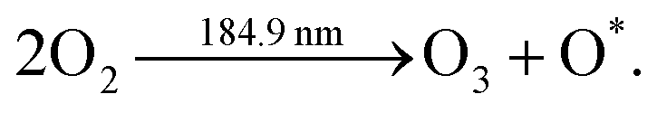 | (1) |
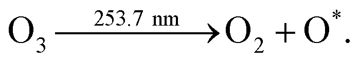
Furthermore, the ozonolysis process involves the decomposition of ozone to produce a high energy oxygen radicle O* upon exposure to UV light of 253.7 nm wavelength, shown by the following equation,
 | (2) |
The highly reactive atomic oxygen reacts with the material to clean the contaminants from the surface of the material. Also, it increases the oxygen-rich stoichiometric properties and surface functionalities and creates defects in the material upon prolonged exposure.
Field emission
The field electron emission investigation, viz. current density (J) versus applied electric field (E) and emission current (I) versus time (t) were measured in a planar ‘diode’ configuration at a base pressure of 1 × 10⁻⁸ mbar. A typical ‘diode’ configuration consists of a phosphor coated semi-transparent screen (a circular disc having a diameter of 4 cm) as an anode. The cathode (pristine and UV/O3 treated NiCo2O4) was pasted on a stainless steel holder with the help of carbon tape which is connected to a linear motion drive. Before recording the FE measurements, pre-conditioning of the cathode was carried out by maintaining it at ∼2 kV for 30 minutes, so as to remove loosely bound particles or contaminants by residual gas ion bombardment. FE measurements were performed at a constant separation of ∼1000 μm, between the anode and cathode. The emission current was measured on a Keithely electrometer (6514) with a sweeping dc voltage applied to the cathode with a step of 40 V (0–40 kV, Spellman, U.S.). Using a computer-controlled data acquisition system, the field emission current stability was recorded at the pre-set (5 μA) current value. The reproducibility of the FE results was checked for two samples synthesized under identical conditions.Computational details
We have executed the theoretical calculations using the Density Functional Theory (DFT) code VASP24–27 combined with PAW–GGA as the exchange–correlation functional28 for the simulations. The plane wave cutoff energy is 500 eV and the Brillion zone is sampled employing a Monkhorst–Pack29 mesh of 8 × 8 × 1 and 8 × 8 × 8 k-points for surface and bulk structure, respectively. We have considered the convergence criterion for Hellmann–Feynman forces as 0.01 eV Å−1 and total energy convergence as 10−6 eV.Results and discussion
Well defined diffraction peaks confirm the phase formation and crystallinity of the as-synthesized material by XRD analysis. Fig. 1 shows the comparison of the XRD pattern of pure NiCo2O4 and UV/O3 treated NiCo2O4, abbreviated as NCO and NCO-UVT, respectively. The sharpness of the diffraction peaks indicates the high crystallinity of the as-grown samples. The representative peaks at 2θ values of 18.9, 31.1, 36.6, 38.2, 44.6, 55.2, 59.1, and 64.9 can be indexed to (111), (220), (311), (222), (400), (422), (511), and (440) planes of the cubic spinel crystalline phase of NiCo2O4 (JCPDS No. 73-1702) belonging to the Fd![[3 with combining macron]](https://www.rsc.org/images/entities/char_0033_0304.gif) m space group (No. 227). Fig. S2 (ESI†) shows the diffraction pattern of NiCo2O4-UVT with the corresponding Rietveld refinement. The inset shows the crystallographic structure derived from the experimental results. Well fitted parameters obtained by the Rietveld plot with fair R-Bragg = 0.190 and goodness of fit = χ2 = 1.55 show good agreement between the calculated and experimental data. The lattice parameters for NiCo2O4-UVT and NiCo2O4 are estimated to be 8.135 Å and 8.11 Å, respectively. A notable change in the lattice parameters refers to the formation of a spinel structure with ionic deficiency. The slight shift (0.189) in the peak belongs to (220) plane towards lower angle also suggests the formation of oxygen vacancy defects.30,31
m space group (No. 227). Fig. S2 (ESI†) shows the diffraction pattern of NiCo2O4-UVT with the corresponding Rietveld refinement. The inset shows the crystallographic structure derived from the experimental results. Well fitted parameters obtained by the Rietveld plot with fair R-Bragg = 0.190 and goodness of fit = χ2 = 1.55 show good agreement between the calculated and experimental data. The lattice parameters for NiCo2O4-UVT and NiCo2O4 are estimated to be 8.135 Å and 8.11 Å, respectively. A notable change in the lattice parameters refers to the formation of a spinel structure with ionic deficiency. The slight shift (0.189) in the peak belongs to (220) plane towards lower angle also suggests the formation of oxygen vacancy defects.30,31
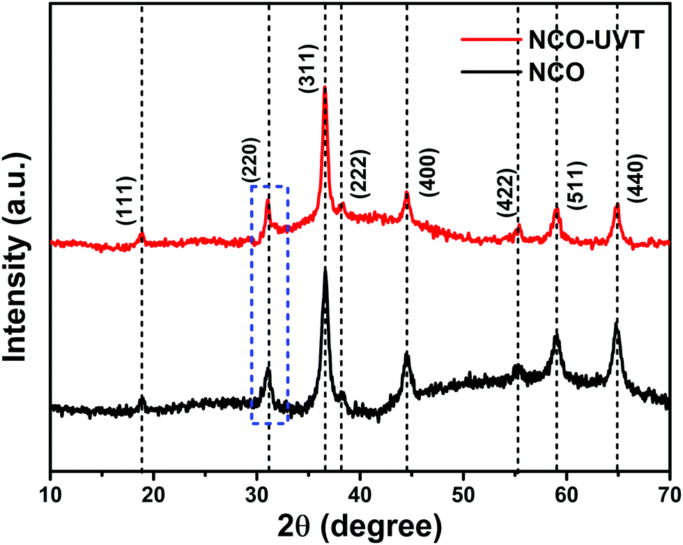 | ||
| Fig. 1 XRD patterns ofNiCo2O4, and NiCo2O4-UVT. | ||
The surface morphology of the samples has been analysed using field emission scanning electron microscopy (FESEM). Fig. 2(a and b) shows an urchin like morphology consisting of numerous nanorods epitaxially growing from the centre. No significant change in the morphology was observed in NiCo2O4 and UV/O3 treated NiCo2O4. The flower like morphology of NiCo2O4-UVT is displayed in Fig. 2(c and d). The chemical composition is confirmed by energy dispersive X-ray spectroscopy (EDAX) analysis. Fig. S1(c and d) (ESI†) illustrates that the molar ratio of Ni![[thin space (1/6-em)]](https://www.rsc.org/images/entities/char_2009.gif) :Co is about 1:2, with a decrease in the atomic oxygen percentage in NiCo2O4-UVT clearly suggesting vacancy formation. The UV/O3 treated NiCo2O4 sample was further characterized by transmission electron microscopy (TEM) Fig. S1(a and b) (ESI†). Urchins like nanostructures are constructed by nanorods with a diameter of 50 to 70 nm covered with particles ranging from 15–30 nm. The random orientation of the lattice phase (HRTEM) manifests the polycrystallinity of UV/O3 treated NiCo2O4. An interplanar distance of 0.28 and 0.25 nm can be assigned to the distances of the (220) and (311) planes of the NiCo2O4 crystal, respectively. The SAED pattern of NiCo2O4 (inset Fig. S1(b), ESI†) shows well-defined rings, which further confirms the polycrystalline intrinsic quality.
:Co is about 1:2, with a decrease in the atomic oxygen percentage in NiCo2O4-UVT clearly suggesting vacancy formation. The UV/O3 treated NiCo2O4 sample was further characterized by transmission electron microscopy (TEM) Fig. S1(a and b) (ESI†). Urchins like nanostructures are constructed by nanorods with a diameter of 50 to 70 nm covered with particles ranging from 15–30 nm. The random orientation of the lattice phase (HRTEM) manifests the polycrystallinity of UV/O3 treated NiCo2O4. An interplanar distance of 0.28 and 0.25 nm can be assigned to the distances of the (220) and (311) planes of the NiCo2O4 crystal, respectively. The SAED pattern of NiCo2O4 (inset Fig. S1(b), ESI†) shows well-defined rings, which further confirms the polycrystalline intrinsic quality.
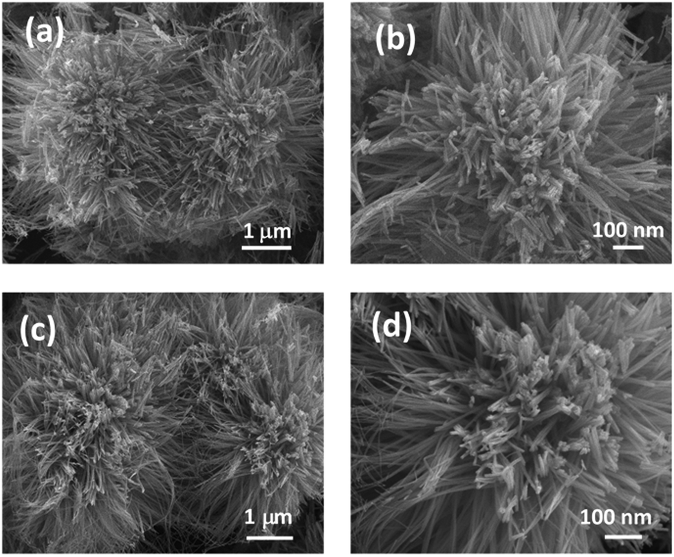 | ||
| Fig. 2 FESEM images of (a and b) NiCo2O4 and (c and d) NiCo2O4-UVT. | ||
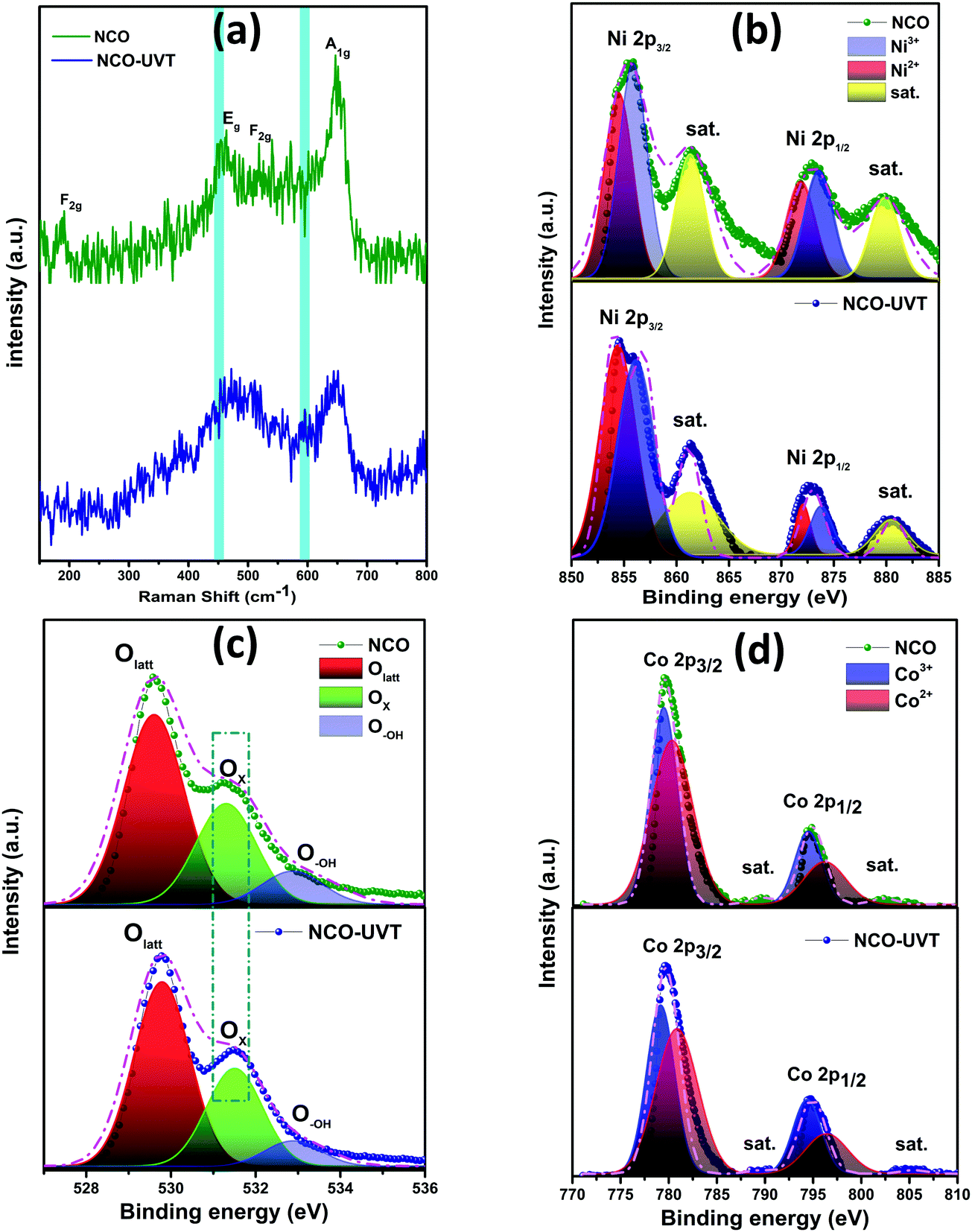
Fig. S3 (ESI†) shows the N2 adsorption–desorption isotherms of NiCo2O4 and UV/O3 treated NiCo2O4. Hysteresis loops of the type IV isotherm (Fig. S3, ESI†) reflect the formation of a mesoporous structure.32 Also, the BET surface area of UV/O3 treated NiCo2O4 is calculated to be 96.06 m2 g−1. The increased surface area of NiCo2O4-UVT is due to defect sites, which reflects the probable oxygen defects.33 The reduction in the surface area resulting from the lattice oxygen vacancy implies the inverse dependency of the lattice oxygen content.34–36 The pore diameter distribution calculated by the Barrett–Joyner–Halenda (BJH) method using the desorption branch of the nitrogen isotherm is shown in Fig. S3(b) (ESI†), a major pore size distribution ranges from 3 to 6 nm. Further detailed compositional analysis including defects due to oxygen vacancies were depicted by the powerful Raman spectroscopic technique. The Raman spectra of both the samples were collected within the spectral range of 150–800 cm−1 are displayed in Fig. 3(a). Raman active vibrational bands correspond to A1g + Eg + 3F2g phonon excitation modes, reassuring the polarization selection rules for an ideal spinel structure.37 Peaks appearing at 191, 515 and 617 cm−1 are attributed to the F2g mode whereas the peaks at 652 and 456 cm−1 correspond to the A1g and Eg modes of vibration. Spectra from both the samples show Co–O and Ni–O vibrations. Signals belonging to the –OH group were not observed hence confirming the decomposition of hydroxide species after thermal treatment. The peak assigned to 652 cm−1 of the A1g mode depicts the stretching of the oxygen atoms at the octahedral sites associated with Co3+ ions in the tetrahedral sites, however, a notable reduction in the same peak may indicate the formation of defects.38 In the detailed observation of Raman bands (Fig. S4(a), ESI†), a sudden peak at 595 cm−1 indicates the formation of oxygen vacancies. The peaks at 456 and 515 cm−1 correspond to the combined vibration of octahedral and tetrahedral oxygen present in the lattice.39 The blue shift at 453 cm−1 in the NiCo2O4-UVT spectrum confirms the oxygen vacancy defect creation and is displayed in Fig. S4(a) (ESI†).40
 | ||
| Fig. 3 (a) Raman spectra of NiCo2O4, and NiCo2O4-UVT. Comparison of high resolution XPS spectra of NiCo2O4, and NiCo2O4-UVT (b) Ni2p, (c) O1s and (d) Co2p. | ||
XPS analysis was performed to study the defects and oxygen vacancies as well as for the structural and compositional analysis. Fig. S4(b) (ESI†) shows the recorded survey spectra. The comparative high resolution XPS spectra of Co2p, Ni2p and O1s of NiCo2O4 and NiCo2O4-UVT is illustrated in Fig. 3(b–d). a well-defined Gaussian fitting method was implemented for the deconvolution of the core level elemental spectra. The best fitted spectra for Ni 2p with two spin orbit doublet and two shakeup satellites (denoted by Sat.) are displayed in Fig. 3(b). The peaks around the binding energy of 854 and 871 eV are assigned to the Ni2+ state and the peaks at 855 and 872 eV are attributed to the Ni3+ state, respectively. The atomic ratios of each element were obtained by the comparison of the covered area obtained by the fitting of curves, as summarized in Table S1 (ESI†). The fitted peak area in high resolution Ni 2p spectra shows a significant reduction in intensity by a slight degree, implying the reduction of Ni3+ to Ni2+. Also, the higher Ni3+/Ni2+ atomic ratio for UV/O3 treated NiCo2O4 indicates the formation of defects due to oxygen vacancies at the surface.41,42 The O defects that are formed may be attributed to the B-type of oxygen vacancy as the charge balance is counted by partial substitution Ni3+ for Ni2+ at the octahedral B-sites which indicates the decreased interaction of the Ni–O vacancy with octahedral Ni and increased interaction between tetrahedral Ni and O.38,55–57 Relatively not much change in the atomic ratio of the Co 2p spectra is observed. The peaks at 780 and 796 eV belong to Co2+ whereas the peaks at 779 and 794 eV are ascribed to the Co3+ state.43 Besides, the core level spectra of O 1s with three major peaks provide the confirmation of oxygen vacancy defect formation after UV/O3 treatment. The typical metal–oxygen (O2−) bonding is represented by the peak at around 529 eV. The peak at a slightly higher binding energy of 533 eV can be observed due to the coordination of the hydroxyl (–OH) species of adsorbed water molecules on the surface and defect caused due to the low oxygen coordination content.58 The obvious peak at 531 eV is mainly attributed to defects sites and oxygen vacancy sites.44,45 The relative enhancement in the Ox peak clarifies the oxygen deficient region in the lattice. Also, the high Ox ratio in NiCo2O4-UVT indicates the increased oxygen vacancies and low coordination on M–O bonds. Thus, core level O 1s spectral features enable the understanding of oxygen vacancy creation when exposed to UV/O3 treatment.
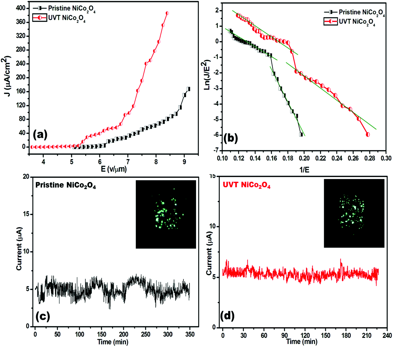
The typical plot of the emission current density (J) as a function of the applied electric field (E) is shown in Fig. 4(a). From the (J–E) plot, the turn on field, defined as the field required to draw emission current density of ∼1 μA cm−2 is found to be 5.69 and 4.38 V μm−1 for the pristine and UV/O3 treated NiCo2O4, respectively. While the threshold field (the field at which the current density starts to shoot up exponentially is termed as threshold field at ∼10 μA cm−2) is 6.21 and 5.32 V μm−1 for the pristine and UV/O3 treated NiCo2O4 emitters, respectively. Interestingly a high emission current density of ∼386 μA cm−2 has been extracted from the UV treated NiCo2O4 emitter at a relatively lower applied electric field of 8.40 V μm−1, than the pristine (∼168 μA cm−2 emission current density at 9.15 V μm−1 applied electric field). The comparative field emission properties of both the emitters are listed in Table 1.
 | ||
| Fig. 4 FE characteristics of pristine and UV/O3 treated NiCO2O4 emitters (a) J–E plot; (b) F–N plot; emission current stability (I–t) plot; (c) pristine and (d) UV/O3 treated NiCo2O4. FE images are shown in the insets of (c and d). The images display a number of tiny spots corresponding to the emission from the most protruding edges of the emitters. | ||
| Field emitter | Turn on filed at 1 μA cm−2 (V μm−1) | Threshold field at 10 μA cm−2 (V μm−1) | Maximum emission current density drawn (μA cm−2) |
|---|---|---|---|
| NiCo2O4 | 5.69 | 6.21 | 168 |
| UVT-NiCo2O4 | 4.38 | 5.32 | 386 |
The FE characteristics were further analysed using the Fowler–Nordheim (FN) theory. The relationship between the current density and applied electric field can be represented as,
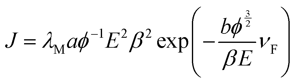 | (3) |
Emission current stability is one of the essential parameters for a field emitter to be considered for practical application. A plot of the emission current (I) as a function of time (t) is depicted in Fig. 4(c). The emission current stability plots were recorded at a pre-set current of 5 μA for more than 3 hours. The emission current stability for the UV treated NiCo2O4 emitter is found to be very good and characterized by a very low number of fluctuations about the mean current value (∼μA) compared to the pristine one. The fluctuations can be attributed to adsorption/desorption of residual gaseous species on the emitter surface.48 The FE image is shown in the inset of Fig. 4(c and d). The image displays a number of tiny spots, corresponding to the emission from the most protruding edges of the emitters.
Theoretical results and discussion
For this simulation, we have considered the spinel structure of NiCo2O4 whose DFT optimized bulk structure is displayed in Fig. 5(a). The computed lattice parameter is 8.09 Å, agreeing well with the experimental value of 8.11 Å.49 In spinel NiCo2O4, the Ni ions are octahedrally coordinated with oxygen ions and Co ions are tetrahedrally coordinated, as depicted in Fig. 5(a). DFT optimized Ni–O and Co–O bond lengths are 1.93 and 1.92 Å, respectively. Fig. 5(b) shows the relaxed structure of bulk NiCo2O4 with two O vacancy introduced in it due to UV/O3 treatment. | ||
| Fig. 5 DFT optimized bulk structure of (a) NiCo2O4 and (b) NiCo2O4 with O vacancy; blue, red and pink spheres indicate Ni, Co and O atoms respectively. | ||
To acheive modification of the electronic properties, in Fig. 6 we have plotted electronic density of states for pristine NiCo2O4 and NiCo2O4 with O vacancy. We can see that the bulk NiCo2O4 has only electronic states in the lower spin channel at the Fermi level. This signifies that bulk NiCo2O4 is half-metallic in nature, agreeing with the results from the literature.50 When O vacancy is introduced, half-metallicity is lost as we can see the electronic states in both spin channels are around the Fermi level in Fig. 6(b). Also, there is an enhancement in the states which may increase the conductivity of the material.
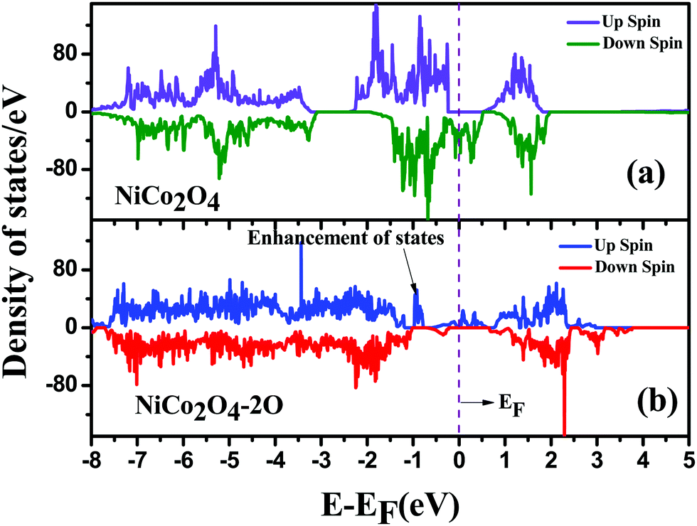 | ||
| Fig. 6 Density of States for (a) bulk NiCo2O4 and (b) bulk NiCo2O4 with double oxygen vacancy; the Fermi level is shown by a dotted line. | ||
To calculate the work function of the material, we have generated surface of NiCo2O4 from the relaxed bulk structure and performed geometry optimization. The relaxed structures of the NiCo2O4 surface without and with O vacancy are depicted in Fig. 7(a).
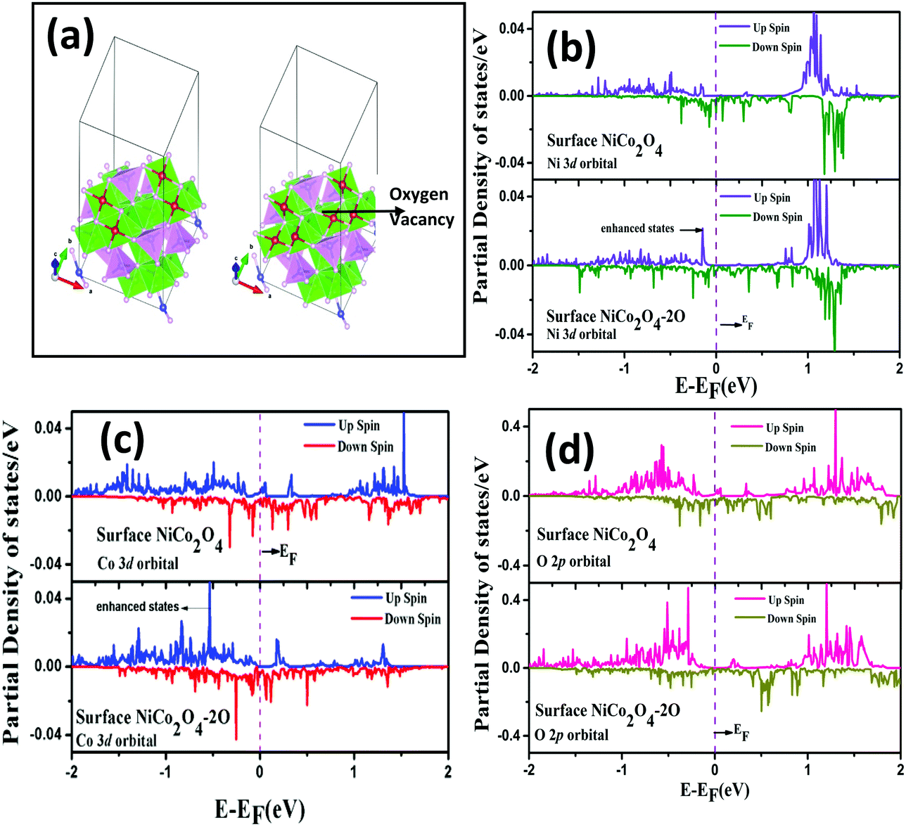 | ||
| Fig. 7 (a) DFT optimized surface structure of (right) NiCo2O4 and (left) NiCo2O4 with O vacancy; blue, red and pink spheres indicate Ni, Co and O atoms respectively, (b) partial density of states of the Ni 3d orbital for the NiCo2O4 surface before (upper panel) and after (upper panel) the 2 oxygen vacancies, (c) partial density of states for Co 3d orbital for the NiCo2O4 surface before (upper panel) and after (upper panel) the 2 oxygen vacancies and (d) partial density of states for the O 2p orbital of the NiCo2O4 surface before (upper panel) and after (upper panel) the 2 oxygen vacancies; the Fermi level is shown by a dotted line. | ||
Computation of work function
To provide theoretical support for enhanced field emission properties of UV/O3 treated NiCo2O4, we computed the work function for the surface of NiCo2O4 before and after O vacancy (UV/O3 treatment) using the following expression,| Φ = EVac − EF | (4) |
For NiCo2O4, EF = 1.91776 eV and EVac = 7.50 eV. So, the computed work function is found to be 5.59 eV, which is in good agreement with the earlier reported value of 5.53 eV.16,51 For NiCo2O4 with oxygen vacancy, EF = 1.85521 eV and ϕ = 7.07 eV and the value of work function is 5.22 eV. So, we can see that there is substantial reduction in the value of work function which is one of the reasons for improved field emission performance for the UV treated NiCo2O4. A similar reduction in work function is obtained for the case of graphene oxide supported VSe2.52 Oxygen vacancy leading to defects in the structure may be one of the reasons for the reduction in the work function.
In order to achieve modification of electronic orbitals, in Fig. 7(b–d), we have plotted the 3d orbital of Ni and Co and 2p orbital of O before and after the O vacancy in the NiCo2O4 surface. We can see that for 3d orbitals of Ni and Co around the vacancy, there is an enhancement in the electronic states near the Fermi level due to the introduction of O vacancy, whereas for the O 2p orbital near the vacancy, there is a slight reduction in the states near the Fermi level. So, there is charge gain by the 3d orbitals of Ni and Co close to the vacancy and there is charge loss for the 2p orbital of the O atom near the vacancy. So, the UV/O3 treatment leads to a rearrangement of the electronic charges near the O vacancy leading to a reduction in the work function which justifies the improved field emission properties after UV/O3 treatment.
Conclusion
The UV/O3 treated NiCo2O4 emitter exhibits enhanced FE behaviour in contrast to the pristine NiCo2O4 emitter, in terms of lower values of turn-on and threshold fields, and competency to deliver large emission current density at a relatively lower applied field. Using extensive DFT calculations, we have studied the modifications in electronic properties of spinel NiCo2O4 due to the introduction of O vacancy as a result of UV/O3 treatment. The O vacancy makes enhancement in electronic states near the Fermi level. There is a rearrangement of electronic charges near the vacancy attributing to a substantial reduction in work function which supports the improved field emission characteristics measured in the experiment after UV/O3 treatment. The computed work function reduces when oxygen vacancy is introduced on the surface of pristine NiCo2O4 which justifies the enhancement in the field electron emission after UV/O3 treatment which supports the experimental findings. Thus, the material with induced oxygen vacancy defects can be further used for FE applications.Conflicts of interest
Authors declare no conflict of interest.Acknowledgements
This work was financially supported by the Department of Science and Technology (DST)-SERB Early Career Research project (Grant No. ECR/2017/001850), the DST-Nanomission (DST/NM/NT/2019/205(G)), and the Karnataka Science and Technology Promotion Society (KSTePS/VGST-RGS-F/2018-19/GRD NO. 829/315). BC thanks Dr.Nandini Garg and Dr T. Sakuntala for the support. BC also acknowledges Dr S. M. Yusuf and Dr A K Mohanty for their support and encouragement. We also acknowledge the BARC computer center where this work was carried out, and thank the staff for their help.References
- V. A. Guzenko, A. Mustonen, P. Helfenstein, E. Kirk and S. Tsujino, Microelectron. Eng., 2013, 111, 114–117 CrossRef CAS.
- Y. Saito, S. Oishi, S. Yamazaki, H. Nakahara, H. Murata and T. Ohno, in 2016 29th International Vacuum Nanoelectronics Conference (IVNC), 2016, pp. 1–2.
- G. Z. Yue, Q. Qiu, B. Gao, Y. Cheng, J. Zhang, H. Shimoda, S. Chang, J. P. Lu and O. Zhou, Appl. Phys. Lett., 2002, 81, 355–357 CrossRef CAS.
- K. L. Jensen, Phys. Plasmas, 1999, 6, 2241–2253 CrossRef CAS.
- X. Li, M. Li, L. Dan, Y. Liu and T. Chuanxiang, Phys. Rev. ST Accel. Beams, 2013, 16, 123401 CrossRef.
- L. Chen, H. Yu, J. Zhong, L. Song, J. Wu and W. Su, Mater. Sci. Eng., B, 2017, 220, 44–58 CrossRef CAS.
- A. K. Singh, S. R. Suryawanshi, M. A. More, S. Basu and S. Sinha, Appl. Surf. Sci., 2017, 396, 1310–1316 CrossRef CAS.
- C. M. Collins, R. J. Parmee, W. I. Milne and M. T. Cole, Adv. Sci., 2016, 3, 1500318 CrossRef PubMed.
- T. Guo, M.-S. Yao, Y.-H. Lin and C.-W. Nan, CrystEngComm, 2015, 17, 3551–3585 RSC.
- P. K. Bankar, S. Ratha, M. A. More, D. J. Late and C. S. Rout, Appl. Surf. Sci., 2017, 418, 270–274 CrossRef CAS.
- S. B. Kokane, S. R. Suryawanshi, R. Sasikala, M. A. More and S. D. Sartale, Mater. Chem. Phys., 2017, 194, 55–64 CrossRef CAS.
- S. Ratha, R. T. Khare, M. A. More, R. Thapa, D. J. Late and C. S. Rout, RSC Adv., 2015, 5, 5372–5378 RSC.
- K. K. Naik, R. T. Khare, M. A. More, D. J. Late and C. S. Rout, RSC Adv., 2016, 6, 29734–29740 RSC.
- S. M. Ansari, S. R. Suryawanshi, M. A. More, D. Sen, Y. D. Kolekar and C. V. Ramana, Chem. Phys. Lett., 2018, 701, 151–156 CrossRef CAS.
- S. V. Bhosale, S. R. Suryawanshi, S. V. Bhoraskar, M. A. More, D. S. Joag and V. L. Mathe, Mater. Res. Express, 2015, 2, 95001 CrossRef.
- K. K. Naik, R. T. Khare, R. V. Gelamo, M. A. More, R. Thapa, D. J. Late and C. S. Rout, Mater. Res. Express, 2015, 2, 95011 CrossRef.
- M. Pathak, J. R. Jose, B. Chakraborty and C. S. Rout, J. Chem. Phys., 2020, 152, 64706 CrossRef CAS PubMed.
- Q. Li, L. Zeng, J. Wang, D. Tang, B. Liu, G. Chen and M. Wei, ACS Appl. Mater. Interfaces, 2011, 3, 1366–1373 CrossRef CAS PubMed.
- W. Qiu, H. Xiao, M. Yu, Y. Li and X. Lu, Chem. Eng. J., 2018, 352, 996–1003 CrossRef CAS.
- Y. Zhu, X. Ji, Z. Wu, W. Song, H. Hou, Z. Wu, X. He, Q. Chen and C. E. Banks, J. Power Sources, 2014, 267, 888–900 CrossRef CAS.
- P. M. Koinkar, D. Yonekura, R.-I. Murakami, T. Moriga and M. A. More, Mod. Phys. Lett. B, 2015, 29, 1540030 CrossRef.
- K. F. Chen, K. C. Chen, Y. C. Jiang, L. Y. Jiang, Y. Y. Chang, M. C. Hsiao and L. H. Chan, Appl. Phys. Lett., 2006, 88, 193127 CrossRef.
- S. B. Fairchild, T. C. Back, P. T. Murray, M. M. Cahay and D. A. Shiffler, J. Vac. Sci. Technol., A, 2011, 29, 31402 CrossRef.
- G. Kresse and J. Hafner, Phys. Rev. B: Condens. Matter Mater. Phys., 1993, 47, 558–561 CrossRef CAS PubMed.
- G. Kresse and J. Hafner, Phys. Rev. B: Condens. Matter Mater. Phys., 1994, 49, 14251–14269 CrossRef CAS PubMed.
- G. Kresse and J. Furthmüller, Comput. Mater. Sci., 1996, 6, 15–50 CrossRef CAS.
- G. Kresse and J. Furthmüller, Phys. Rev. B: Condens. Matter Mater. Phys., 1996, 54, 11169–11186 CrossRef CAS PubMed.
- J. P. Perdew, K. Burke and M. Ernzerhof, Phys. Rev. Lett., 1996, 77, 3865–3868 CrossRef CAS PubMed.
- H. J. Monkhorst and J. D. Pack, Phys. Rev. B: Solid State, 1976, 13, 5188–5192 CrossRef.
- C. Li, X. Han, F. Cheng, Y. Hu, C. Chen and J. Chen, Nat. Commun., 2015, 6, 7345 CrossRef CAS PubMed.
- D. Lim, H. Kong, C. Lim, N. Kim, S. Se and B. Sh, Int. J. Hydrogen Energy, 2019, 44, 23775–23783 CrossRef CAS.
- C. Nethravathi, C. R. Rajamathi, M. Rajamathi, X. Wang, U. K. Gautam, D. Golberg and Y. Bando, ACS Nano, 2014, 8, 2755–2765 CrossRef CAS PubMed.
- M. Lammert, M. T. Wharmby, S. Smolders, B. Bueken, A. Lieb, K. A. Lomachenko, D. D. Vos and N. Stock, Chem. Commun., 2015, 51, 12578–12581 RSC.
- V. Makwana, Y.-C. Son, A. Howell and S. Suib, J. Catal., 2002, 210, 46–52 CrossRef CAS.
- H. Hayashi, K. Hirao, M. Toriyama, S. Kanzaki and K. Itatani, J. Am. Ceram. Soc., 2001, 84, 3060–3062 CrossRef CAS.
- D. Prieur, W. Bonani, K. Popa, O. Walter, K. W. Kriegsman, M. H. Engelhard, X. Guo, R. Eloirdi, T. Gouder, A. Beck, T. Vitova, A. C. Scheinost, K. Kvashnina and P. Martin, Inorg. Chem., 2020, 59, 5760–5767 CrossRef CAS PubMed.
- P. Bhojane, S. Sen and P. M. Shirage, Appl. Surf. Sci., 2016, 377, 376–384 CrossRef CAS.
- M. N. Iliev, P. Silwal, B. Loukya, R. Datta, D. H. Kim, N. D. Todorov, N. Pachauri and A. Gupta, J. Appl. Phys., 2013, 114, 33514 CrossRef.
- P. Nayak, M. Sahoo and S. K. Nayak, Ceram. Int., 2020, 46, 3818–3826 CrossRef CAS.
- L. Wu, Q. Zhang, J. Hong, Z. Dong and J. Wang, Chemosphere, 2019, 221, 412–422 CrossRef CAS PubMed.
- D. Yan, W. Wang, X. Luo, C. Chen, Y. Zeng and Z. Zhu, Chem. Eng. J., 2018, 334, 864–872 CrossRef CAS.
- Y. Liu, P. Liu, W. Qin, X. Wu and G. Yang, Electrochim. Acta, 2019, 297, 623–632 CrossRef CAS.
- M. Pathak, D. Tamang, M. Kandasamy, B. Chakraborty and C. S. Rout, Appl. Mater. Today, 2020, 19, 100568 CrossRef.
- H. Yuan, J. Li, W. Yang, Z. Zhuang, Y. Zhao, L. He, L. Xu, X. Liao, R. Zhu and L. Mai, ACS Appl. Mater. Interfaces, 2018, 10, 16410–16417 CrossRef CAS PubMed.
- Y. Zeng, Z. Lai, Y. Han, H. Zhang, S. Xie and X. Lu, Adv. Mater., 2018, 30, 1802396 CrossRef PubMed.
- A. A. Al-Tabbakh, M. A. More, D. S. Joag, I. S. Mulla and V. K. Pillai, ACS Nano, 2010, 4, 5585–5590 CrossRef CAS PubMed.
- L. M. Baskin, O. I. Lvov and G. N. Fursey, Phys. Status Solidi, 1971, 47, 49–62 CrossRef CAS.
- P. K. Bankar, P. S. Kolhe, P. R. Mutadak, A. Kawade, K. M. Sonawane and M. A. More, Phys. E, 2021, 125, 114363 CrossRef CAS.
- Y. Bitla, Y.-Y. Chin, J.-C. Lin, C. N. Van, R. Liu, Y. Zhu, H.-J. Liu, Q. Zhan, H.-J. Lin, C.-T. Chen, Y.-H. Chu and Q. He, Sci. Rep., 2015, 5, 15201 CrossRef CAS PubMed.
- X. Shi, S. L. Bernasek and A. Selloni, J. Phys. Chem. C, 2016, 120, 14892–14898 CrossRef CAS.
- C. Zhang, X. Geng, S. Tang, M. Deng and Y. Du, J. Mater. Chem. A, 2017, 5, 5912–5919 RSC.
- S. Ratha, P. Bankar, A. S. Gangan, M. A. More, D. J. Late, J. N. Behera, B. Chakraborty and C. S. Rout, J. Phys. Chem. Solids, 2019, 128, 384–390 CrossRef CAS.
- X.-B. Shi, M.-F. Xu, D.-Y. Zhou, Z.-K. Wang and L.-S. Liao, Appl. Phys. Lett., 2013, 102, 233304 CrossRef.
- S. Bai, Z. Wu, X. Xu, Y. Jin, B. Sun, X. Guo, S. He, X. Wang, Z. Ye, H. Wei, X. Han and W. Ma, Appl. Phys. Lett., 2012, 100, 203906 CrossRef.
- C. Wu, L. liu, R. Xu, K. Zhang, C. Zhen, L. Ma and D. Hou, Mater. Sci. Eng., B, 2021, 263, 114886 CrossRef CAS.
- K. Zhang, C. Zhen, W. Wei, W. Guo, G. Tang, L. Ma, D. Hou and X. Wu, RSC Adv., 2017, 7, 36026–36033 RSC.
- P. D. Battle, A. K. Cheetham and J. B. Goodenough, Mater. Res. Bull., 1979, 14, 1013–1024 CrossRef CAS.
- P. Wang, C. Wu, C. Zhen, G. Li, C. Pan, L. Ma and D. Hou, Phys. B, 2019, 561, 147–154 CrossRef CAS.
Footnote |
| † Electronic supplementary information (ESI) available. See DOI: 10.1039/d1ma00032b |
| This journal is © The Royal Society of Chemistry 2021 |