
 Open Access Article
 This Open Access Article is licensed under a Creative Commons Attribution-Non Commercial 3.0 Unported Licence
Photoconductive PbSe thin films for infrared imaging†
Mool C.
Gupta
 *,
Joel T.
Harrison
and
Md Toriqul
Islam
*,
Joel T.
Harrison
and
Md Toriqul
Islam
Department of Electrical and Computer Engineering, University of Virginia, Charlottesville, VA 22904, USA. E-mail: mg9re@virginia.edu
First published on 18th April 2021
Abstract
Lead selenide (PbSe) emerged 70+ years ago for its unique photoconductive sensitivity to the mid-wave infrared (MWIR) spectrum; however, new and exciting research continues to ignite interest in this material to this day. PbSe has endured primarily due to its high IR responsivity at room temperature (uncooled), large-area application space, and low-cost fabrication. PbSe has a large nominal Bohr exciton radius (∼46 nm) that allows bandgap tuning from 0.27 eV to as far as 2.0 eV by manipulation of grain size and morphology. This review aims to summarize the most recent state-of-the-art progress in PbSe photoconductivity research, including synthesized quantum-dots (QDs) and novel manufacturing methods.
 Mool C. Gupta | Mool C. Gupta received his PhD degree in physics from Washington State University, Pullman, WA, USA, in 1973. He was a Postdoctoral Fellow at Cornell University and a Senior Research Fellow at the California Institute of Technology. From 1998 to 2005, he was Director of the Applied Research Center at Old Dominion University. Since 2005, he has been the Langley Distinguished Professor in the Electrical and Computer Engineering Department at the University of Virginia. He is the Founding Director of the NSF Industry/University Cooperative Research Center for Lasers and Plasmas at the University of Virginia. His current research interests include the applications of high-powered lasers for solar cell manufacturing, thermophotovoltaics, photonic devices, laser micro-texturing of surfaces, and infrared detectors. He is Editor-in-Chief of the Handbook of Photonics, CRC Press, 1st and 2nd edition. He has over 250 scientific publications in various technical journals and has been awarded 29 U.S. and international patents. Dr Gupta is also a Fellow of the Optical Society of America, a Fellow of IEEE society, an Inductee of the Kodak Inventor's Gallery, Chair of the NRC NASA Technology Roadmap Materials Panel, and Principal Investigator for DARPA, ARO, NASA, NSF, DOE, and AFSOR. |
 Joel T. Harrison | Joel Harrison is a PhD student at the University of Virginia and employee for the Department of Navy. He received his Master degree from the University of Virginia in 2014 in electrical engineering with a focus on solid state physics and material science. He received a bachelors degree in Electrical Engineering from Virginia Commonwealth University in 2001. From 2001 to 2009, he worked in the semiconductor industry as a failure analysis engineer for Motorola in Phoenix, AZ and Infineon Technologies in Richmond, VA. From 2009 to present, he has worked for the Department of Defense where he specializes in microelectronics and failure analysis. |
 Md Toriqul Islam | Md Toriqul Islam is currently a PhD student in the Department of Electrical and Computer Engineering at the University of Virginia. He received his Master of Science in Electrical and Computer Engineering from the University of Alabama at Birmingham, Master in Information Technology from the University of Dhaka, and Bachelors in Electrical Engineering from the Military Institute of Science and Technology, Bangladesh. Before starting his graduate studies, Toriqul was a lead software engineer at Samsung R&D Institute Bangladesh. His current research focuses on thin-films development, electrical and optical characterization, laser pulse annealing, laser processing for semiconductor devices, and photodetectors. |
1. Introduction
Infrared (IR) imagers usually detect thermal radiation in the form of photons emitting from objects and mapping (patterns) to identify any object's presence or the object's properties itself. IR radiation wavelengths are generally categorized into four regions, near-wavelength IR (NIR) ranges from 0.78 to 1.4 μm, short-wavelength IR (SWIR) ranges from 1.4 to 3.0 μm, mid-wavelength IR (MWIR) ranges from 3.0 to 5.0 μm, and long-wavelength IR (LWIR) ranges from 8.0 to 12.0 μm.1,2 Lead salts such as lead selenide (PbSe) and lead sulfide (PbS) are the first semiconductor materials used as IR detectors and still the leading choice of detectors for IR sensing applications operating in the 1 to 5 μm spectral range.3,4 All the forms of PbSe, such as polycrystalline, monocrystalline, and QDs, are being researched and used for IR imaging applications. Many new nanostructures and technologies have been investigated in the last few decades to reduce the cost and improve the IR detection system's performance. However, the current IR detection technology is costly, difficult to fabricate, and operates in the low-temperature range.The PbSe thin films have unique intrinsic physical properties and band structure, widely used for the NIR and MWIR range applications. The PbSe polycrystalline thin films are widely used for IR detectors,5–9 IR Photoluminescence,10 diode laser,11 up-conversion imaging devices,12 imaging sensor devices,13–16 thermoelectric coolers,17 and IR solar cells.3 Recently, the PbSe QD thin films are also being used for IR photodetectors,18–21 photovoltaic cells,22–28 IR electroluminescent,29 thermoelectric,30,31 laser,32 and field-effect transistor (FET).33–35
Some of the most common applications of IR imaging sensors are night vision, military missile tracking, surveillance systems, search and rescue, research, medical imaging, food production, quality control, industry defect imaging, precision temperature measurement, environmental sensing, meteorology, climatology, and exoplanet exploration.1,2,10,18 The MWIR and LWIR are important for lossless free-space communications and astronomy due to their high transparency in the atmosphere. IR detection is a non-contact and non-destructive method, which is very useful for defect detection in electronic circuits, semiconductor chips, device control, paved road condition control, and various other monitoring activities.1 Nowadays, military aircraft use high-performance IR cameras to scan the battlefield in weak visibility conditions. IR radiations mostly come from a thermal source and are less absorbed and scattered in the atmosphere compared to the visible light, which can provide a large amount of information of the source such as temperature, compounds, geometry, location in space, and atmosphere of the source.2 Even molecular level information can be identified because each molecule has its unique IR signature. Various medical tools such as blood vein monitoring, brain trauma detection, diabetic neuropathy, thermography, and cancer cell detection work based on IR imaging.1
The lead salt materials (PbS and PbSe) offer some advantages over competing materials, but some challenges need to be addressed. Various detector materials are being used for IR detection, which should be small in size, lightweight, low power, and low-cost systems.36 One of MWIR imaging sensors' essential requirements is that they should be operable in the cryogenic temperature range to achieve a satisfactory signal-to-noise ratio (SNR).6 It is required to prevent the thermal generation of charge carriers; otherwise, it will increase the noise in the device performance.5,36 The uncooled polycrystalline PbSe is an excellent choice for this regime. It can outperform other materials such as single crystalline indium antimonide (InSb) and mercury cadmium telluride (HgCdTe, also known as MCT).6 The indium arsenide (InAs), InSb, and HgCdTe photodetectors also work properly at very cold temperatures, but their system performance requires the increased size, cost, and complexity.36 The pyroelectric or bolometric materials-based photodetectors can be considered for a broad range of wavelengths, but they have low sensitivity and slow response speed.36 The indium gallium arsenide (InGaAs) offers a good choice for photodetection (both standard and extended). The standard InGaAs photodiode provides excellent sensitivity and high speed but is limited to upper wavelength sensitivity up to 1.7 μm.36 The extended InGaAs photodiode also provides considerable sensitivity, but it can only be extended up to 2.3 μm.36 So, InGaAs photodiode is not a good choice for general applications considering the 3 to 5 μm wide range of wavelengths.
The PbSe offers reduced size, weight, and low power requirements for IR imaging and sensing devices.6 The lead salt narrow bandgap IV–VI semiconductor alloys have provided an exceptional degree of freedom in IR detector design because of their energy bandgap tunability, high optical absorption coefficient, high electron mobility, and low charge carrier thermal generation rate.1,5,17 The PbSe is a direct bandgap material, which shows a narrow bandgap of around 0.27 eV at room temperature (RT).5,19 The bulk PbSe semiconductor exhibits some crucial characteristics such as crystal structure of cubic form, large exciton Bohr radius, small effective masses for both electrons and holes, and a large dielectric constant.19 The large dielectric constant leads to a low exciton binding energy, and thus charges are almost free due to low scattering loss,37 which inherently favors total photocurrent generation. This semiconductor compound has a multivalley band structure with band extrema at the L point of the Brillouin zone (BZ).10 The energy bands of PbSe are arranged in a nearly mirror-like configuration relative to the Fermi level. The band structure of both bulk and monolayer PbSe is shown in Fig. 1. Energy bands are shown by considering different symmetry points, where the valence band maximum and the conduction band minimum of bulk PbSe lie at the L point of the BZ. The band structure is mirror-like due to the similar effective mass of electrons and holes in the material (me* ≈ mh*). It has the advantage of reducing the nonradiative Auger recombination by one or two orders of magnitude compared to the narrow gap III–V and II–VI semiconductors.10
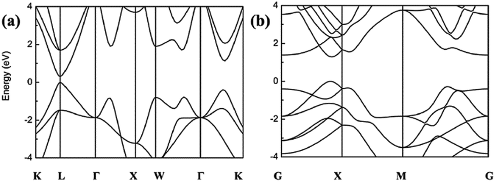 | ||
| Fig. 1 Band structures of (a) bulk and (b) monolayer PbSe.38 (Reproduced from ref. 38 with permission of The Royal Society of Chemistry, Journal of Materials Chemistry C.) | ||
A photoconductor works like a resistor, where the conductivity changes with the number of incident photons. Photons with energy higher than the PbSe bandgap energy are absorbed to produce electron–hole pairs, which controls the total conductivity of the PbSe.36 Since the PbSe is a small bandgap material; it can detect low-energy photons. The PbSe thin films can be made both ambipolar and unipolar; thus, they show both n-type and p-type conductivity. The conductivity of the as-deposited polycrystalline PbSe depends on the ratio of Pb and Se, Pb-rich films are n-type, and Se-rich films are p-type.39,40,69
The molecular beam epitaxy (MBE) grown monocrystalline PbSe on CaF2/Si(111) heterostructure by Li et al.41 showed majority carriers mobility of 647 cm2 V−1 s−1 and 9.875 × 103 cm2 V−1 s−1 respectively at 300 K and 77 K, which increased to 1.073 × 103 cm2 V−1 s−1 and 29.912 × 103 cm2 V−1 s−1 with an in situ surface treatment. Zhao et al.42 indicated the annealing effect on mobility for a similar structure, where PbSe monocrystalline film showed p-type carrier mobility of 400 cm2 V−1 s−1 and 1.05 × 104 cm2 V−1 s−1 respectively at 300 K and 77 K, which increased to 530 cm2 V−1 s−1 and 2.19 × 104 cm2 V−1 s−1 after annealing at 300 °C for 2 hours.42 Tetyorkin et al.43 reported the n-type mobility of monocrystalline PbSe film as 1.5 × 104 cm2 V−1 s−1 at 77 K, using the thermal evaporation technique.
For monocrystalline PbSe films, mobility is relatively high, but it is much lower for the polycrystalline films due to heavy disorder in the film.44 The mobility of polycrystalline n-type PbSe film varies between 60–120 cm2 V−1 s−1 at RT and increases with decreasing temperature, such as 210 cm2 V−1 s−1 at 100 K, deposited using the physical vapor deposition (PVD) process.7 The mobility of polycrystalline p-type PbSe film was reported as 68.5 cm2 V−1 s−1 at RT, using the chemical bath deposition (CBD) process.45 Recently, Yang et al.46 reported high mobility of 8.323 × 103 cm2 V−1 s−1 at RT for nanostructured polycrystalline PbSe thin film using electron beam evaporation and O+ beam implantation followed by an annealing process.
Recent reports show both ambipolar and unipolar quantum-confined FET with different electron and hole mobility. Zhang et al.18 reported an intrinsic PbSe QD vertical FET with hole mobility and electron mobility of 2.5 cm2 V−1 s−1 and 2 cm2 V−1 s−1, respectively. Oh et al.47 reported quantum-confined single nanowire (SNW) PbSe FETs using a deposited p-type film with a hole mobility of 65 (±10) cm2 V−1 s−1 at RT and 1000 (±100) cm2 V−1 s−1 at 20 K. Oh et al.47 also reported predominantly n-type PbSe SNW FET with electron mobility of 10 (±5) cm2 V−1 s−1 at RT and 100 (±10) cm2 V−1 s−1 at 20 K.
Most of the literature suggested that oxygen could convert n-type PbSe into p-type and form a p–n junction.7 Humphrey indicated that halogens could be used to convert a PbSe film from n-type to p-type; however, the maximum sensitivity was accomplished only through the use of oxygen.48,49 Qui et al. showed that iodine plays the most critical role in the sensitization procedure of p-type PbSe photoconductor, where oxygen can be used to improve the PbSe sensitivity.9 While, Zhao et al. proposed a p–n junction charge separation model by showing that the iodine converts the surface of p-type PbSe crystallites into n-type.50
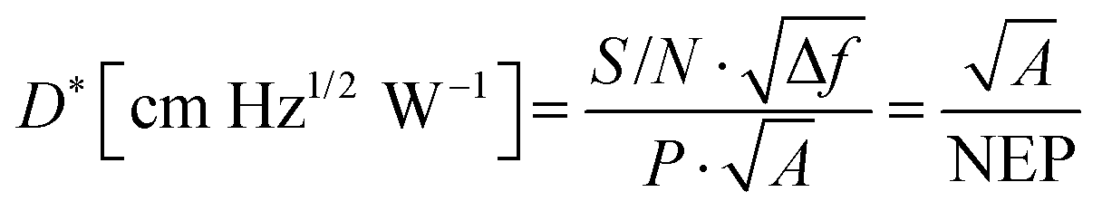
It has been shown that the p–n junction characteristics strongly influence the photoconductivity performance, and it also can provide optimal sensitivity at the highest possible operating temperature.7 Usually, a simple voltage divider bias circuit is used to measure the radiation, where the voltage across the load resistor varies with incident radiation.36 So far, the highest photo detectivity (D*) of the MWIR PbSe thin films is reported as of 4.2 × 1010 cm Hz1/2 W−1 at RT by using a CaF2 antireflection (AR) coating.8 Without the AR coating, the highest D* is reported as 2.8 × 1010 cm Hz1/2 W−1 at RT.9
The PbSe bulk resistance is temperature-dependent, typically in the order of 3%/°C.36 Sun et al.51 showed that the electrical resistivity of the sputtered polycrystalline PbSe thin film has negative temperature dependence, measured in the 25 °C to 100 °C temperature range. Recently Ganguly et al.44 also reported linear response of resistance versus temperature (R–T) and benchmarked with Northrop Grumman Corporation (NGC) polycrystalline PbSe detectors, shown in Fig. 5(c). Generally, lead chalcogenide QD films exhibit positive temperature coefficients of resistance except for PbSe QD films, in which resistance decreases with increasing temperature.52–54 When bulk resistance of the sensitized polycrystalline PbSe thin film decreases due to the rising temperature, then the bolometric signal overlaps with the photoconductive signal. During film performance analysis, it becomes very difficult to differentiate between bolometric signal and photoconductive signal. The best solution is to keep the photodetector under constant temperature.
Several researchers have reported PbSe QDs based devices by shifting bandgap energy allowing different optoelectronic applications to cover a large spectral range from MWIR to NIR.19 The strong quantum confinement effect is used to tune the bandgap by controlling their size (the QD diameter).18,19 The PbSe QDs offer attractive optoelectronic properties such as multiple exciton generation (MEG), small exciton binding energy, large dipole moment, high purity crystals, strong light absorption, and good photo-stability, which ultimately increases the quantum efficiency.6,18,19 The PbSe QD is a promising material for IR imaging applications, which also have the advantages of low-cost solution processability, flexibility, and easy scale-up production compared to other photodetector semiconductors.19 However, the conductivity and photoresponsivity of the QDs are limited by the low carrier mobility because the photocurrent is proportional to the carrier mobility.18 Great efforts need to be focused on improving the carrier concentration, carrier mobility, and carrier lifetime.
The performance of lead salt IR detectors depends on many factors of the fabrication process, such as crystallization, annealing atmosphere, including gas concentration and temperature, number of annealing stages, the final size of crystallites, and crystal morphology.3 So, understanding the operation mechanism and providing a quantitative experimental model for optimization of those factors is crucial to have higher efficient PbSe IR detectors. Researchers have used different types of fabrication methods to prepare PbSe devices, such as CBD, PVD, chemical vapor deposition (CVD), MBE, electrodeposition (ED), atomic layer deposition (ALD), synthesized QD (SQD), and e-beam defined QD (EBDQD). Among those, CBD and PVD are most widely used by industry due to their high-quality crystal structure.6 The physical properties of the developed PbSe thin films are controlled by different parameters such as the method of deposition, substrate material, substrate temperature, cleanliness of the substrate, rate of deposition, deposition periods, and the background pressure.17 There is still research going on for PbSe thin film process improvement of existing deposition technology, as well as some new techniques are offered such as photochemical, sonochemical, pulsed laser deposition (PLD), and laser-sintered deposition (LSD).17
Monocrystalline PbSe photovoltaic detectors are also getting researchers' attention for MWIR and LWIR large format focal plane array (FPA) thermal imaging applications.3 With advanced fabrication technology, it is possible to integrate photodetectors with electronic readouts to make detector FPAs, which is now one of the key research focus.5 Single crystalline or polycrystalline PbSe thin films can be grown on silicon substrates to fabricate FPA because it allows large area uniformity and easy integration with Si wafer.3 However, it faces a fundamental challenge of high dislocation density because of a large mismatch in lattice constant and thermal expansion coefficient between PbSe film and Si wafers.3 Further research is needed to reduce film defects and their impact on charge recombination. Several techniques are already being experimented with and proposed, such as buffer layer and strained layers techniques, lateral growth, selected area growth, and ex situ treatment techniques such as annealing, even though the success is limited due to the nature of fundamental material physics.3
2. Properties
2.1 Intrinsic properties of PbSe
This review focuses on PbSe; however, much of what is covered applies to PbTe and PbS as well. There are many properties of PbSe that attract researchers; its narrow and direct bandgap (0.27 eV)55 and large nominal Bohr exciton radius (∼46 nm)55,56 offer superior versatility for tuning of the spectral photoresponse. The narrow intrinsic (bulk) bandgap of PbSe makes it sensitive to the MWIR regime of the electromagnetic (EM) spectrum. The relatively large Bohr exciton radius enables its strong quantum confinement characteristics. Each of these properties is interesting alone, but combined, it allows for an exceptional ability to shift the bandgap and spectral range of optical photoresponsivity precisely. Furthermore, the large Bohr radius allows relatively reproducible and straightforward thin-film processing to obtain nanocrystals with unique properties. This allows investigations of quantum size effects of a more stable material with dimensions that do not have a large surface to volume ratio.55PbSe attracts interests in both solar cells and thermoelectric research as well. The presence of an intrinsic electric field is imperative for enhancing third-generation solar cells.57 The MEG phenomenon has been explored for the next generation of photovoltaic devices and could play an important role.57 Gordi et al. show that the intrinsic electric field of all Pb-chalcogenides affects the absorptivity spectra yet has a relatively insignificant effect on the MEG quantum probabilities, allowing enhancements in solar cell efficiency.57Table 1 lists the useful properties of PbSe.
| Crystal properties | Physical properties | ||
|---|---|---|---|
| Crystal type | Cubic | Density (g cm−3) | 8.15 |
| Structure | Halite | Lattice constant (Å) | 6.124 |
| Space group | Fm3m | Molecular weight (g mol−1) | 286.2 |
| Electronic properties (293 K) | Thermal properties | ||
|---|---|---|---|
| Bandgap (eV) | 0.26 | Thermal conductivity (W m−1 k−1) | 1.7 |
| Electron mobility (cm2 V−1 s−1) | 1000 | Melting point (°C) | 1067 |
| Hole mobility (cm2 V−1 s−1) | 900 | Heat of formation (kJ mol−1) | 393 |
Many optical properties are energy and wavelength (λ) dependant. Table 2 summarizes the dielectric constant (ε* = ε1 + iε2), complex refractive index (n* = n + ik), absorption coefficient (α) and normal-incidence reflectivity (R). As for thermoelectric properties, recent work by Du et al. has shown that high-pressure sintering (HPS) following mechanical alloying (MA) of PbSe can achieve a figure of merit (ZT) of ∼0.57 at 600 K.59 PbSe is now attracting attention as an alternative to PbTe due to the lower cost of Se compared to Te, high stability, and wider operating temperature.60 Recent work by Ekuma et al. shows evidence of improvements in ZT by introducing defect states in a monolayer of intrinsic PbSe, in the form of Se vacancies.61
| eV | λ (nm) | ε1 | ε2 | n | k | α (cm−1) | R |
|---|---|---|---|---|---|---|---|
| 0.001 | 1![[thin space (1/6-em)]](https://www.rsc.org/images/entities/char_2009.gif) 240000 240000 |
−169.7 | 960.3 | 20.1 | 23.9 | 2.4 × 10³ | 0.92 |
| 0.005 | 248000 |
−94.3 | 322.4 | 11.0 | 14.7 | 7.4 × 10³ | 0.88 |
| 0.01 | 124000 |
−50.1 | 24.8 | 1.7 | 7.3 | 7.4 × 10³ | 0.89 |
| 0.05 | 24800 |
20.2 | 0.2 | 4.5 | 0.02 | 8.7 × 101 | 0.41 |
| 0.1 | 12400 |
22.31 | 4.7 | 0.42 | |||
| 0.2 | 6200 | 23.3 | 4.8 | 0.43 | |||
| 0.3 | 4133 | 25.3 | 1.1 | 5.0 | 0.1 | 3.2 × 10³ | 0.45 |
| 0.4 | 3100 | 24 | 2.9 | 4.9 | 0.3 | 1.2 × 10⁴ | 0.44 |
| 0.5 | 2480 | 0.3 | 1.5 × 10⁴ | ||||
| 1 | 1240 | 0.6 | 5.8 × 10⁴ | ||||
| 1.5 | 827 | 24.6 | 16.6 | 5.2 | 1.6 | 2.4 × 10⁵ | 0.49 |
| 2 | 620 | 20.0 | 21.1 | 5.0 | 2.1 | 4.3 × 10⁵ | 0.54 |
| 2.5 | 496 | 10.3 | 32.4 | 4.7 | 3.4 | 8.7 × 10⁵ | 0.57 |
| 3 | 413 | −9.7 | 24.2 | 2.9 | 4.2 | 1.3 × 10⁶ | 0.65 |
| 4 | 310 | −5.9 | 7.5 | 1.4 | 2.8 | 1.1 × 10⁶ | 0.59 |
| 4.5 | 276 | −4.7 | 5.8 | 1.2 | 2.5 | 1.1 × 10⁶ | 0.57 |
| 5 | 248 | −3.7 | 4.3 | 1.0 | 2.2 | 1.1 × 10⁶ | 0.54 |
One of the most exciting aspects of PbSe is how its properties contrast with other semiconductors. The bandgap of most semiconductors widens with pressure and decreases with temperature, while the bandgap of PbSe narrows with pressure and increases with temperature.63 This is discussed in detail by Wei et al.64 and Svane et al.65 and is related to spin–orbit phenomena as a consequence of band ordering at the L point.66 Using the potential, Ekuma et al. calculated a 1% compression of the lattice parameter for PbSe, resulted in a 0.11 eV bandgap decrease.66 Streltsov et al. showed that with sufficient pressure (13–25 GPa), PbSe transitions from a cubic (NaCl) semiconductor to an orthorhombic (CsCl) metal and superconductor.67
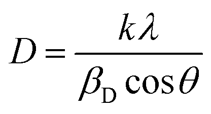
Thin films are susceptible to the coefficient of thermal expansion (CTE) mismatch, which can translate to strain. This is particularly important in stacked thin-films and nanocrystalline geometries where confinement occurs. Many groups monitor crystalline strain with X-ray diffraction (XRD); however, one must be mindful of the convolution between the XRD parameters used for determining nonuniform crystalline strain and grain size.68 The changes in stress and changes in grain size can be hard to delineate. Nonuniform induced lattice strain broadens XRD peaks and changes full-width half-maximum (FWHM) parameters. Thermal annealing can relieve nonuniform lattice strains; however, it can also grow and cause grain merging. The FWHM parameter is used to determine grain size using Scherrer's equation.
 | (1) |
The value D represents the diameter of the average grain based on a dimensionless factor of (k) close to unity, the wavelength of the X-ray source (λ), the full-width half-maximum (βD), and the Bragg angle (θ).
Transmission Electron Microscopy (TEM) is the most accurate method for determining domain size and variation as well as crystalline quality, albeit TEM analysis offers only a localized representation of the material properties.
While single-crystalline PbSe can be readily produced with MBE or ALD, polycrystalline forms of PbSe offer many advantages to IR sensor applications. This will be described in more detail under the photoconductivity section. Due to the absorption coefficient (Table 2) and to maximize the S/N of the photoresponse, polycrystalline thin films of 200 nm–2.0 μm thickness are generally targeted. Polycrystalline grain size can be modulated in many ways like substrate temperature and surface conditions but typically ranges from 100 to 500 nm. It should be noted that crystallite size can be the same or smaller than gain size. Grain size should not be confused with crystallite size as individual grains are often polycrystalline.
2.2 Photoconductivity
The high electron and hole mobility of intrinsic (bulk) PbSe allows for highly electrically conductive polycrystalline thin films at RT. This, as well as good optical absorption properties, enables high photoresponsivity under photon excitation. The blue-shift in the band absorption edge is the result of the strong confinement characteristics of PbSe. This shift is so easily achieved, many groups have shifted the bandgap from the intrinsic gap of 0.27 eV to as much as 1.8 eV, corresponding to wavelengths of 4.6 μm to 690 nm, respectively.While PbSe has been used as an infrared responsive material for over 70 years, the photoconductive mechanisms are still under debate. The models depend heavily on the grain morphology, sensitization, and deposition/synthesis method. PbSe films are often near stoichiometrically balanced (1:1); however, this is highly dependent on the deposition method and conditions during material deposition. It is well understood that intrinsic PbSe (p-type or n-type) is not IR responsive-without additional processing referred to as sensitization. While this section focuses on the intrinsic properties of PbSe (bulk), photoconductivity cannot be described without a description of the process required to enable this property.
Some groups refer to sensitization as oxidation or thermal annealing in the air; however, while the process is simple and many groups can achieve IR responsivity with relative ease, the conditions have significant implications for maximizing photon absorption, achieving linear responsivity (Fig. 2), and detectivity. There are a variety of accepted models for how thermal oxidation enables an IR response in PbSe. The general understanding is that oxidation between PbSe grain boundaries (core–shell p–n junction model) or layered film interfaces (vertical p–n junction model) forms a potential barrier that acts as an electron trap. The incident photon generates an e–h pair, and the barrier traps the electron, resulting in enhanced hole carrier lifetime. This influences the conductivity and, under an external electric field, translates to a change in conductance. Optimization of sensitization for applications such as FPA usually utilizes halogen doping, often iodine. This is necessary to increase the IR photoconductivity signal. Hechster et al. observed that annealing in a chlorine environment, as opposed to oxygen, improved the signal-to-noise ratio in thin films of PbSe.70
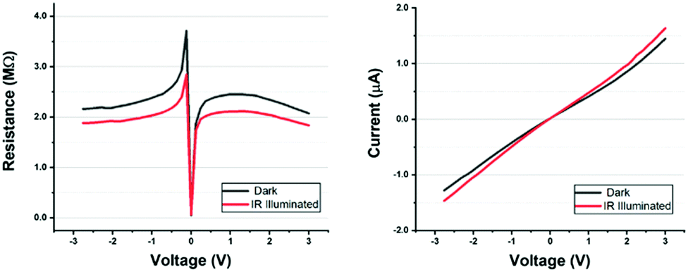 | ||
| Fig. 2 Photocurrent response curves of a sensitized PbSe polycrystalline thin film (2 μm), dark and illuminated, with a 4–5 μm light source (18 mW cm−2).71 (Reproduced from ref. 71 with permission of the Elsevier, Journal of Alloys and Compounds.) | ||
3. Thin-film fabrication
Research in PbSe-based photodetector development can be broken down into two categories based on the targeted wavelength of photosensitivity. Historically, PbSe has been used for MWIR photodetector applications based on the intrinsic (bulk) optical bandgap of 0.27 eV, centering the IR photosensitivity around a wavelength of 4.4 μm. In the recent decade, however, much of the research in PbSe is focused on exploiting the quantum confinement phenomena by modulating and reducing the crystallite size below the Bohr radius. The modulation of photosensitivity of PbSe can be shifted to a wavelength as short as 690 nm, with an optical bandgap of 1.8 eV. This potentially allows the broadband photosensitivity of PbSe to span across MWIR, SWIR, NIR, and into the optically visible regime (690 nm–4.4 μm). For this reason, a delineation will be made between reviewing PbSe-based photodetector fabrication for MWIR application and those intended for shorter wavelengths.
3.1 Fabrication of MWIR PbSe thin films
Vast amounts of research have gone into increasing the infrared responsivity of PbSe thin films and better understanding the properties around its intrinsic (bulk) optical bandgap (0.27 eV), centered around a wavelength of ∼4.4 μm. The majority of progress in this area has been accomplished using the CBD method, which is also the preferred deposition method for achieving the highest IR responsivity.72–75The CBD process is low-cost, and the setup is straightforward, requiring commonly available chemical lab facilities and equipment. Various precursor chemistries shown in Table 3 are used as sources of lead and selenium. The deposition rates and film properties are primarily controlled by chemical concentrations, bath temperature, pH, and surfactants. The morphology can vary significantly from a very highly ordered cubic polycrystalline thin-film to a vertically columnar grain or even loosely packed precipitated (just-touching) crystal particles. The substrate conditions (material type, crystallinity, roughness, and type) can influence the polycrystalline orientation from a random mix of crystalline orientation76 to a single preferred orientation.77
| Source | Year | Substrate | Recipe |
|---|---|---|---|
| Grozdanov84 | 1998 | Glass, polyester | 10–12 mL 0.5 M Pb(NO3)2 + 2 M NaOH + 10 mL 1 M Na2SeSO3. T = 70 °C; pH = 10. Selenosulfate: 1 M Na2SO3 + 1 M Se followed by sintering |
| Sarkar85 | 2006 | Glass | 60 mM Pb(CH3COO)2 + 50 mM Na2SeSO3 + 0.6 M KOH. pH = 13. Selenosulfate: 0.5 M Na2SO3 + 0.2 M Se |
| 2006 | 60 mM Pb(CH3COO)2 + 50 mM Na2SeSO3 + 160 mM TSC. pH = 10.5. Selenosulfate: 0.5 M Na2SO3 + 0.2 M Se | ||
| Hankare86 | 2003 | Glass | 10 mL 0.25 M Pb(NO3)2 + 1 M tartaric acid + 1 M KOH + 10 mL 0.25 M Na2SeSO3. T = 4.85–25 °C |
| Kassim87 | 2010 | Glass | 20 mL 0.15 M Pb(NO3)2 + 10 mL triethanolamine + 20 mL 0.15 M Na2SeO4. T = 25–80 °C; pH = 6 |
| Jang72–74 | 2019 | SiO2/Si | 1 M Pb(CH3COO)2 + 1 M CH4N2Se + KOH. T = 80 °C; t = 1 h; pH = 10. Oxidation at 460 °C for 6.25 min. Iodization at 300 °C for 6.25 min |
| Templeman88 | 2014 | GaAs | 60 mM Pb(CH3COO)2 + 50 mM Na2SeSO3 + KOH. pH > 13. Selenosulfate: 0.5 M Na2SO3 + Se |
| Gorer89 | 1995 | Glass | 60 mM Pb(CH3COO)2 + 160–320 mM TSC + 50 mM Na2SeSO3 + KOH. pH = 10. Selenosulfate: 0.5 M Na2SO3 + 0.2 M Se (70 °C, several hours) |
| 60 mM Pb(CH3COO)2 + 0.6–4.3 M KOH + 50 mM Na2SeSO3. pH > 13. Selenosulfate: 0.5 M Na2SO3 + 0.2 M Se (70 °C, several hours) |
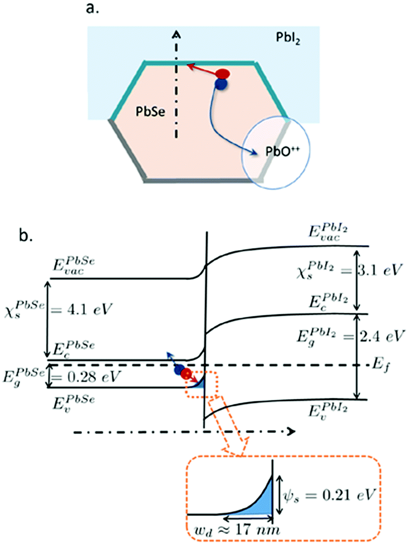 | ||
| Fig. 3 Interface model and band diagram of a junction between PbSe grains and PbI2 layer.44 (Reproduced from ref. 44 with permission of the AIP Publishing, Journal of Applied Physics.) | ||
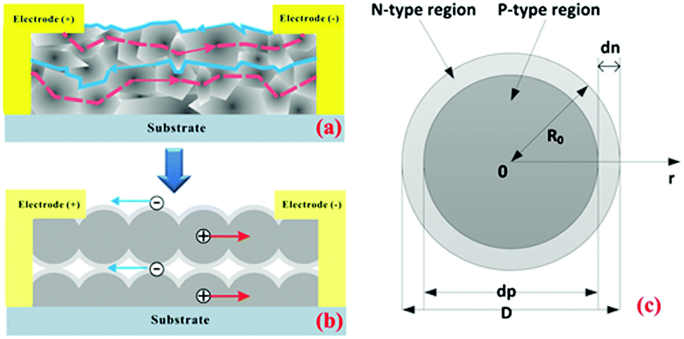 | ||
| Fig. 4 Core–shell junction interface for the charge separation model for PbSe.50 (Reproduced from ref. 50 with permission of the AIP Publishing, Journal of Applied Physics.) | ||
All discussion of MWIR sensitization of PbSe should be prefaced with a heavy emphasis on the fact that all films are not created equal. The many ways to form, deposit or synthesize PbSe along with significant variations of morphology and the volatility of selenium is crucial when comparing one group's results from another. Many oxidized forms of PbSe exhibit p-type conduction properties with larger bandgaps (Table 5). Also, while iodine is used as an n-type dopant in PbSe, the iodization process reacts with PbSe and the many forms of PbxSeyOz to form a layer of PbI2, which is a p-type semi-insulator (Eg = 2.3 eV). While a particular process may form a specific p or n-type PbSe film, all thermal processing, with or without oxygen or iodine, impact the stoichiometry of PbSe and begin to transition and change the homogeneity of the film regardless of the deposition method. The initial film conduction type, film morphology, thickness, film density, grain size, porosity are just a few film properties that should be considered before making any conclusions. Many researchers have successfully formed different junctions with different combinations of sensitization. For example, Yang et al.78 reported MWIR response with oxidation alone on p-type PbSe but not on n-type, and Jang et al.72 reported a p–p isotype heterojunction on a layered film stack of PbI2 on p-type PbSe.
Many groups reported that both oxidation and iodization must occur to achieve any appreciable IR photoresponse in thin-films of PbSe.72–75,79,80 Until recently, the understanding is that oxidation of the top ∼50% of the polycrystalline PbSe film, as well as along grain boundaries, produces forms of PbSeO3 or Pb3O2(SeO3), which acts as a large bandgap, potential barrier, selectively trapping electrons and extending hole carrier lifetime to allow transport to electrodes. The role of iodine was accepted by most as aiding in the recrystallization and assisting in the controlled incorporation of oxygen into the PbSe lattice. Regardless of the model, the electron traps must be formed for PbSe to have a photoconductive response to IR light. Whatever the way it is achieved, the sensitization process results in a significant increase in the film's conductivity.
Many believe the purpose of iodine is to aid in the solid-state sintering and rapid recrystallizaiton75 of PbSe and PbSeO3. Golubchenko et al. reported that the presence of iodine reduces the formation temperature of the oxyselenites such as PbSeO3 by more than 100 K.81,82 While this may be one of its roles, recent work by Jang et al. and Suh et al. show that the symbiotic relationship between oxygen and iodine is multipurpose.73,75,83 Regardless of the order and role of oxygen and iodine, both thermal processes reduce selenium content in the upper part of the PbSe film to form PbI2 and various PbSexIyOz, and PbSexO1−x complexes. The net results are reduced selenium content, the formation of lead oxide/PbI2 layers, and the diffusion of iodine and oxygen into the PbSe film and/or along PbSe grain boundaries. Both Jang et al. and Suh et al. show that iodine incorporation in the actual CBD deposition bath is necessary to incorporate iodine into the PbSe lattice during the film deposition, in addition to a subsequent thermal iodization process to form a PbI2 layer.73,75,83
Jang et al. reported the chemical reactions during oxidations and iodization, respectively.60 Qiu et al. reported the iodization of PbSe releasing Se gas during PbI2 formation.90
| 6PbSe + 9O2 → 2Pb3O2(SeO3) + 4SeO2(g) | (2) |
| 2Pb3O2(SeO3) + 6I2 → 6PbI2 + 2SeO2(g) + 3O2(g) | (3) |
| PbSe + I2 → PbI2 + Se(g) | (4) |
Jang et al.60 reported and proved experimentally that the upper part of the PbI2 layer acts as passivation, a high Eg barrier (Eg = 2.3 eV), and aids in reducing the non-radiative recombination of e–h pairs. Jang also reports the interaction of the oxidation and iodization is complex and thoroughly explains the significance of band alignment of the materials and the location of the Fermi level.72 However, Jang states iodization without oxidation can result in rapid conversion of the entire thin-film to PbI2. This agrees with reaction (4) above in that iodization, alone, will volatilize all the Se to form a 100% PbI2 film. Jang et al. report that following iodization, XRD data suggest very little oxygen remains in a crystalline form of their fully sensitized film. They suggest that the oxidation of the top layer serves both to better control the iodization process in the formation of the top PbI2 layer and form electron traps by incorporating oxygen into the bottom layer PbSe crystals and grain boundaries. It is stated that iodization without oxidation may be possible under appropriate process conditions.74 Oxygen is still necessary to act as electron traps, but this suggests sufficient oxygen content may be incorporated into the PbSe lattice during the CBD deposition process and thermal iodization. This is supported by documented improvements in photoconductivity for thermal evaporative deposition of PbSe under poor vacuum conditions, allowing oxygen incorporation during film formation.74
Suh and Humphrey et al. state that “the photoconductive responsivity is proportional to the resistivity and the response time of the sensor. Therefore, for a photoconductive sensor to have a high responsivity, it is necessary to have a high resistivity and long response or carrier lifetime”.48,49,75 Suh et al. reports that vapor pressure during iodization following oxidation play a significant role in forming of the PbI2.75 Suh further concludes that iodine atoms both inside and outside of the PbSe microcrystals may work together to induce effective solid-state sintering leading to the redistribution of oxygen atoms in the effective atomic sites.75
Contrary to the commonly accepted sensitization process, several groups have adopted a hybrid sensitization process whereby iodization occurs first by annealing in an I2 and O2 atmosphere at 220 °C for 15 minutes followed by annealing in O2 only, at 450 °C for 1 hour.79,80,91 The reduced hybrid iodization temperature suggests that minimal reaction occurs between the iodine and the PbSe, possibly lending to slow diffusion of iodine along grain boundaries. Even if only interstitially, the presence of the iodine may help promote the recrystallization and incorporation of oxygen into the bottom PbSe in the subsequent oxidation step at 450 °C. Suppose Golubchenko et al. are correct, and the presence of iodine reduces the formation temperature of oxyselenites by 100 °C; in that case, this process may be successfully forming the critical electron traps inside the PbSe crystallite and along grain boundaries.81,82 Any PbI2 formed during the hybrid-iodization step would reflow during the subsequent 450 °C oxidation process given the 402 °C melting point of PbI2.
Many groups report XRD data revealing different forms of PbSe-oxides and PbSeI-oxides. High IR responsivity is achieved in thin films of PbSe spanning all forms. Some groups report better performance with one form; however, the evidence is supported with empirical data only. Regardless, the one common property of all forms of these lead-oxide and lead-iodide compounds is a large bandgap (Table 4), providing an electron trapping barrier.
| Lead chalcogenide | Bohr radius (nm) | Bulk bandgap Eg (eV) | QD Eg range (eV) |
|---|---|---|---|
| PbS | 18 | 0.41 | 0.60–1.6 |
| PbSe | 46 | 0.28 | 0.35–1.7 |
| PbTe | 150 | 0.31 | 0.60–1.1 |
A fascinating study by Hechster et al. shows that annealing in a chlorine environment, instead of oxygen, improved the signal-to-noise ratio in thin films of PbSe.70 While many groups report evidence of high IR responsivity in PbSe thin-films with a particular setup, there is still a significant amount of contradicting data suggesting a more systematic bottom-up approach may be necessary to better understand the complexities of the sensitization of PbSe thin-films for MWIR photodetector.
Ganguly et al. published the first comprehensive physics-based material-to-system model for monolithic polycrystalline PbSe photodetectors for a CBD process developed by industry.44 Characterization data from fabricated photodetectors were fed into the model, interconnecting the band structure of the PbSe film to the SPICE-based compact model from Northrop Grumman and the University of Virginia experimental teams. This accounted for effects such as material variability and operating conditions and was validated on two independent sets of experiments by benchmarking I–V, low bias R–T, and D*–V data provided by experiments.44 The results of these data are shown in Fig. 5.44 Additionally, the group projected future photodetector performance based on anticipated materials improvements and operating conditions. This is the first step towards developing a comprehensive model for PbSe photodetectors design.
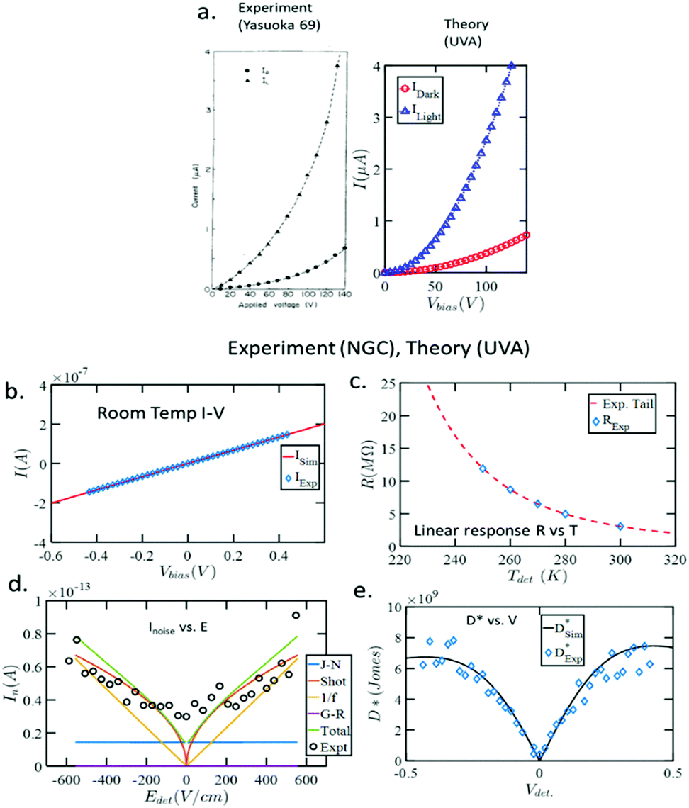 | ||
| Fig. 5 (a) Benchmarking dark and light IV of a classic experiment (1970).95 (b) Benchmarking RT IV of detectors fabricated at Northrop Grumman (2017). (c) Linear response RT benchmarked with NGC detectors. (d) Benchmarking of various noise mechanisms with experimentally measured noise. (e) Benchmarking of DV between the theoretical model and the experimentally measured detector performance.44 (Reproduced from ref. 44 with permission of the AIP Publishing, Journal of Applied Physics). | ||
While this section is specifically focused on CBD fabrication for MWIR photodetector application, Borousan et al. reported an impressive level of grain size control using a CBD method they refer to as coprecipitation92 developed by Shiravizadeh et al. Borousan's work was intended for solar applications in the Vis-NIR regime; however, they show by using surfactants in the CBD process, they can modulate the morphology and crystallite size from 2.0 μm to 35 nm.92 The surfactant-free sample produced with the coprecipitation method (larger grains) can make PbSe films in the MWIR regime.
The use of surfactants in the CBD process for MWIR photodetectors is promising. Smirnova et al. reported the addition of ammonium iodide (NH4I) in the CBD bath, influencing the grain size and morphology. It did not impact the ∼1:1 stoichiometry of the PbSe. In contrast, the concentration of NH4I in the bath linearly affects the Pb:I atomic ratio and increases the PbSe lattice parameter suggesting iodine is being incorporated into the PbSe crystals during deposition.93 This work does not report any influence on the oxidation step of the sensitization process nor impact on IR photoconductivity or responsivity. Subsequent work reported by Yurk et al. and Maskaeva builds on this by evaluating the influence of adding antioxidants and NH4I to the CBD bath during PbSe deposition.94
Several antioxidants were evaluated by Yurk and were found to heavily impact the stability of the selenurea precursor chemistry for up to five days. Higher alkalinity was found to increase the decomposition of selenurea, but Na2SO3 and C6H8C6 were found to have a stabilizing effect. A small amount of reduction in the PbSe lattice constant and an increase in the share of nanocrystals and optical bandgap were also reported (0.78–1.0 eV).94 Maskeave et al. combined the NH4I and antioxidants and reported a PbSe crystallite size ranging from 60 to 2 nm; however, the bandgaps reported, post anneal, were found to range from 0.27 to 0.35 eV.96 It is unclear what caused the discrepancy between their reported optical bandgap. Maskaeva also introduced both NH4I and performed a thermal anneal. The anneal may have merged the crystallites to a scale above the Bohr radius of PbSe to achieve an optical bandgap of bulk PbSe. The presence of elevated iodine levels (NH4I) may have influenced PbSe crystal growth and oxygen incorporation into the PbSe grain, making the films optical bandgap correlate to larger crystallite geometry associated with MWIR wavelengths.
PbSe deposition via CBD is reported as being highly sensitive to substrate type and surface conditions with respect to morphology, crystalline preference, and adhesion. Shandalov et al. reported that their CBD process resulted in superior wetting and adhesion to GaAs substrate as opposed to SiO2 and glass.97 They reported poor adhesion and lack of a continuous film for SiO2. Others successfully deposited a high-quality continuous PbSe film on thermally oxidized silicon substrates by roughening the surface for better adhesion and grain nucleation.72–74,83
Kim et al. synthesized colloidal PbSe particles using a novel CBD-like solution-based method and spin-coated to form a PbSe film on various substrates (glass, ITO, and PET). The films were annealed in an Ar atmosphere, and a near-perfect (200) preferential orientation PbSe films were achieved by controlling the acetate (CH3COO−):nitrate (NO3−) ratios. The choice of chemistries modified the polarity of the chemistry, leading to this highly preferred crystalline orientation.98
Kumar et al. deposited a PbSe film on a glass substrate and fully sensitized to achieve an impressive D* of 2.8 × 1010 cm Hz1/2 W−1.76,77 Kumar provides extensive TEM and SAED analysis and thoroughly documents the key finding of this high D* film. A schematic depicting the TEM and SAED results in the layout of a comprehensive picture of the chemical and morphological properties for fabricating high IR responsive PbSe film.
Qiu et al. reported a thin-film fabrication method to better tune a PbSe-based thin-film sensitive to a specific optical bandgap/wavelength.99 They used a two-step CBD process to deposit PbSe NC on top of CdS NCs to form a heterojunction. Instead of growing a film with specific wavelength sensitivity, Qiu formed a PbSe-based film with significant quantum confinement characteristics (blue-shift) followed by thermal annealing to both repair crystalline order, reduce interface defects and grow the PbSe grains (red-shift).
Red-shifting via thermal annealing allows a more controllable means of tailoring the film to a specific IR wavelength as opposed to controlling with only a film deposition process. Thermal annealing potentially offers a linear and cumulative solution of tuning the film bandgap and band alignment. Qui et al. show how with increasing temperature and time, they can adjust the optical sensitivity of a PbSe-QD/CdS heterojunction between Visible to MWIR. With increasing temperature, both crystalline defects are reduced, and the dark photocurrent is suppressed. They achieved a sensitivity Rpeak of 0.36 A W−1 and a D* of 4.2 × 108 cm Hz1/2 W−1 with a cutoff wavelength of 4.2 μm.99
Templeton et al. reported a unique morphology controlled by substrate temperature during their CBD deposition process.100 By varying the substrate temperature between 15–40 °C, they were able to obtain distinct PL signals ranging from 1.9–4.4 μm in wavelength, respectively.100 The deposition rate was slow; however, the columnar morphology could be beneficial for maximizing absorption by scattering light. There was no mention of sensitization.
Rapid progress in using different complexing agents, precursors chemistries, and QD precipitation methods proves CBD has the flexibility to cover the IR spectrum while remaining relatively simple and inexpensive. While other deposition processes are used to grow thin films, CBD is a very mature process, and this assures CBD will remain in heavy use. While other methods are increasing in use and offer advanced process control, there is still a need for material development and process maturation.
The PVD is grouped with thermal evaporation and sputtering from high purity, physical targets in a very controlled chamber environment with precision vacuum, temperature-controlled platens, and a choice between inert and reactive carrier gasses.
These vapor-based processes offer the benefit of a more controlled deposition rate and better uniformity. Sinh et al. used a thermal evaporation process to deposit thin-films of PbSe doped with Cd, CdI, CdSe, and Sn.101 The group deposited layers of these doped and alloyed films on both silicon and glass substrates. The morphology varied from randomly oriented nanocrystals to preferentially oriented cuboids (20–500 nm). They also show a transition from an ordered cuboid morphology to a much smaller and flat film of elongated nanorod101 and control of the morphology with doping and subsequent thermal annealing. The Sn doping significantly influences the morphology, allowing nanorods of 50 nm diameter, yet interestingly had no impact on bandgap (0.27 eV). The Cd and CdI doped samples showed a similar change in morphology with annealing yet showed a significant bandgap shift. Addition results from this group were reported by Saraf and showed similar results with additional optical characterization. The Cd-doped PbSe films were reported of having a bandgap of 0.52–0.54 eV, corresponding to an optical wavelength sensitivity of 2.4–2.3 μm, respectively.102
Sun et al. acknowledged, “the optical and photoelectric properties of PbSe thin-films are intensely affected by the crystal structure which is mainly determined by the growth process.”103 Sun reported results from a thermodynamic simulation, confirmed with experimental results, the optical characteristics of PbSe grain grown via PVD on different substrates. Sun deposited PbSe on monocrystalline silicon substrates of (100) and (111) orientation. They reported the complex relationship between the two primary preferred PbSe (200 & 220) orientations with substrate orientation, and dependency on the interface and strain energy variation.103
Sun et al. reported that the preferred orientations are obtained with variations of interface and strain energies during the growth process.103 It should be noted that some PbSe photodetectors are grown on insulators, such as on thermally grown SiO2, which is amorphous. This is an important finding as control of crystal properties is critical to achieving a repeatable and manufacturable photodetector process.
While many groups chose to continue to perform research on the more mature CBD deposition method, physical vapor deposition will undoubtedly produce mature and enable much more advanced photodetectors as well as other device types. The advantage of tight process controls will become key, and the costs will go down as the volume of demand increases. It is expected that more integration of deposition methods will become more common, as seen with the reports above by Qiu et al.99
3.2 Fabrication for VIS-SWIR PbSe thin films
The vast majority of SWIR to visible photodetector research relating to lead chalcogenides is PbS-based. As a result, PbS is a much more mature and understood material; however, interest in PbSe for photodetectors and photovoltaics is building momentum. Research in PbSe is beginning to eclipse PbS due to its smaller bandgap, larger Bohr exciton radius, and wider QD bandgap range (Table 4). The bandgap can be tuned to large or shorter values by a further change in QD size, and the values shown in Table 4 are just for a limited range based on the cited paper. Eqn (5) is a simplified form of the Brus equation showing the relationship between the bulk bandgap and the effect of quantum confinement in QDs with QD radius (R) and carrier effective mass (m*). PbSe is also gaining traction on PbTe for thermoelectric applications due to its high performance and lower costs.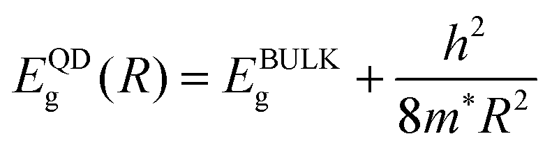 | (5) |
Fabrication of reduced crystallite sizes below the Bohr exciton radius of 46 nm can be accomplished using many different methods, including but not limited to CBD, PVD, and CVD. However, the most successful and widely used method for synthesizing nanocrystal (NC) or QD PbSe, is the hot-injection method. While other methods are capable of producing and modulating PbSe QD size and thus spectral photoresponse, it is unclear how well these methods can repeatably target a specific spectral response for a given application. QD size is just one variable of many that can impact spectral response, so tight process controls must be achievable for any fabrication method to prevail past the research phase. Deposition methods with less process control, such as CBD, may potentially struggle to fabricate on a larger scale and maintain tight process controls such as chemical bath concentrations leading to a cross-wafer nonuniformity and wafer-to-wafer variation. Many research groups using other synthesizing methods for fabricating QD do so by varying process parameters such as temperature to scale the QD size; however, determination of the photoresponse is often limited to optical characterization with photoluminescence (PL) or optical absorption spectra (Tauc plots).
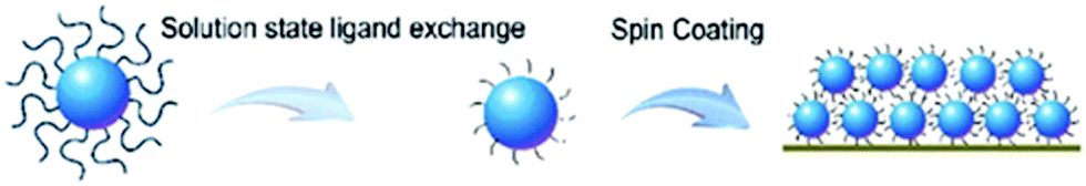 | ||
| Fig. 6 QD Ligand formation and exchange process.108 (Reproduced from ref. 108 with permission of The Royal Society of Chemistry, Energy & Environmental Science.) | ||
Hu et al. report that the most effective and widely-used ligand exchange process uses purely atomic ligands such as iodine and bromine or a hybrid of these halogens with a short organic ligand such as mercaptopropionic (MPA) or ethanedithiol (EDT).107 Hu reports a comprehensive description of the ligand exchange process as well as the entire fabrication process from synthesis to choosing appropriate capping materials for band-aligning metal contacts107 (Fig. 7). The ligand-induced surface dipole presents a means of control over the absolute energy of QD by as much as 0.9 eV, as shown in Fig. 7 (right).
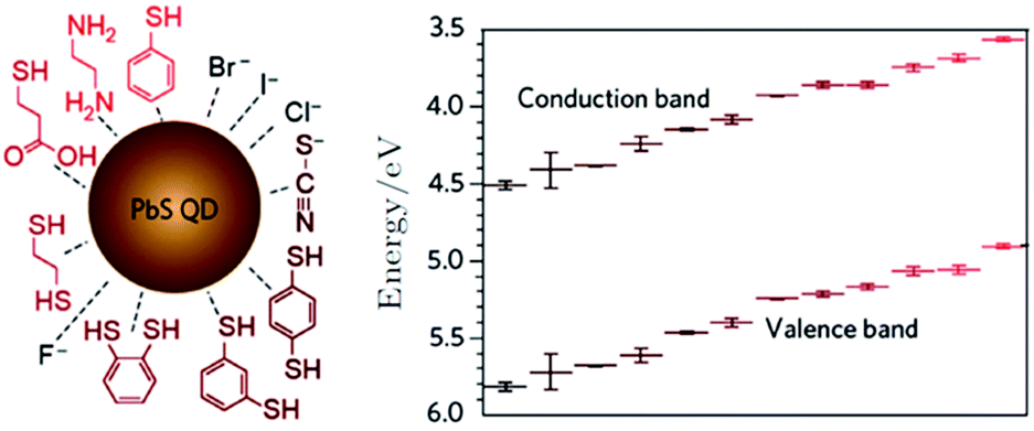 | ||
| Fig. 7 QD Ligand exchange types for PbS with absolute band energies and their respective bandgap shifts with different ligands due to their respective surface dipole.109 (Reproduced from ref. 109 with permission of the American Chemical Society, Nano.) | ||
Dai et al. proposed a new core–shell model where the PbSe core QD is stoichiometrically balanced while the shell (surface atoms) are free of Se and effectively a pure Pb layer.110 It was unclear if this was inherent to the synthesis process; however, this appeared to be the case and is consistent regardless of the Se-precursor, Se-TBP (tributylphosphine), or Se-TOP (trioctylphosphine). Dai reported through convincing and rigorous means that a single layer of Pb exists on the surface of the QDs and was consistent across a population of 18 samples.110
The outer pure-Pb layer of QDs may react and form a passivation layer of PbI2 during the ligand exchange process. Compared to tightly packed grains of PbSe thin films, the QD's higher exposed surface and higher surface to volume ratio allow for a higher PbI2 or PbO/PbSeOx to PbSe ratio. This may provide the necessary electron trapping barrier as well as passivation of the surface. It may also be accomplished without a high-temperature thermal process due to the nanoscale geometries. A native oxide, similar to RT native oxides of silicon, maybe all that is necessary to form a high-bandgap electron trap barrier for QD. Table 5 lists the various forms of PbSe-oxides and PbI2 with their respective bandgaps. The presence of a halogen-based barrier may further improve this minority carrier trapping mechanism.
| Material | Crystal | E g (eV) |
|---|---|---|
| PbSe | Cubic | 0.27 |
| PbSeO3 | Monoclinic | 3.2 |
| PbI2 | Rhombohedral | 2.3 |
| PbO | Orthorhombic | 2.8 |
| PbO | Tetragonal | 1.9 |
| Pb3O4 | Tetragonal | 2.1 |
| Pb12O19 | Monoclinic | 1.3 |
| Pb2O3 | Monoclinic | 1.4 |
| PbO2 | Tetragonal, rutile | 1.5 |
| PbO2 | Tetragonal, columbite | 1.4 |
Shuklov et al. reported a comprehensive review specifically for lead chalcogenide QD synthesis, including an evaluation of all the most effective methods.105 Shuklov provides substantial detail from a chemistry perspective as well as the latest understanding of advantages and disadvantages for each synthesis of PbSe QDs.105 According to Shuklov, there are dozens of methods for synthesizing PbSe QDs, and all come with different trade-offs.
3.3 Discussion on Fabrication of PbSe QD
One interesting observation that is not clearly explained between the bulk property of PbSe versus those exhibiting quantum confinement (blue-shift) is the need for thermal sensitization. As described above (MWIR section), thin-films of PbSe with Eg closer to the bulk level (∼0.35–0.28 eV) require oxidation and iodization to enable any measurable photoconductive response. Many researchers have achieved a substantial photoresponse using QD without thermal oxidation or iodization. Iodine has been shown to impact many parameters in PbSe; however, it is still unclear which are essential to enabling substantial photoconductivity for thin films. The use of halogens in QD films to enable a photoresponse may support the notion that iodine's primary role in PbSe films is to passivate and form a large bandgap barrier for electrons.72 QD also uses halogen-based ligands to shift the bandgap (Fig. 7) by applying their surface dipole and controlling the carrier density. The ligand-induced surface dipole presents a means of control over the total energy of QD by as much as 0.9 eV, as shown in Fig. 7 (right). We know that iodine also acts as a substitution site for oxygen into the PbSe lattice and lowers the activation energy of recrystallization. These may be less critical in QD films as their surfaces are more sensitive to oxygen exposure. Additionally, the large surface to volume ratio may allow a larger percent of PbSe to get more sufficiently doped with oxygen atoms from the colloidal solution and precursor chemistry in the QD synthesis.While a separate thermal sensitization step with oxygen and halogens does not appear to be necessary to enable a high photoresponse for QDs, many researchers are using halogen-based coatings on QDs to replace the organic ligands inherent in the synthesis of QD. Many are finding the benefits of coating QD with halogens (iodine, bromine, and chlorine) to increase conductivity and passivate QDs to stabilize them from degradation due to oxidation.105
It should also be noted that while many researchers have successfully modulated the photoresponse of PbSe nanocrystals between Vis and MWIR, the data is empirically collected, and the correlation between crystallite size and optical spectra is usually performed using Scherrer's formula taken from XRD spectra. While TEM is usually used to determine the size and monodispersing of PbSe QDs, XRD is often used for determining crystallite sizes for more traditional thin film deposition of PbSe. This has many sources of error, and crystallite size correlation to optical spectra varies significantly between literature, even within the same group.94,96 For this reason, much work is needed to address the accuracy and precision for repeatability of any nanocrystal or QD synthesis process and understand these discrepancies. This is expected as this field is in the material development phase. Many challenges lay ahead; however, the progress looks promising for a wide variety of applications from thermoelectric, optoelectronics, photovoltaics, and photodetectors.
Eqn (6) is provided by Moreels et al. for correlating optical bandgap of PbSe QD of various diameters (d) between 2 and 20 nm.105,111 This allows a determination of the spectral position of the first optical transition based on particle size.
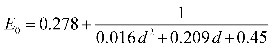 | (6) |
The value E0 represents the optical bandgap of PbSe QDs and d represents the diameter of the QD (Fig. 8).
 | ||
| Fig. 8 Plot of eqn (6)111 showing the relationship between the optical bandgap based on QD diameter. | ||
4. IR photodetector devices
IR detection devices work based on a photo-sensitive material, which can absorb IR radiation and convert the absorbed light into a detectable electrical signal. Semiconductor-based materials are leading this field due to their strong light absorption properties. Other materials are being researched and proposed as an alternative, but their quantum efficiency (QE) is very low. Different types of semiconductor materials (i.e., different bandgaps) are required for detecting different IR ranges. The photodetector performance can be improved by engineering the electronic properties (detectivity and quantum efficiency) of the absorbing material and increasing the coupling of light to the electronic states of the absorbing material. Despite the advantages and ranges of applications of highly sensitive IR cameras, they require cryogenic cooling, which makes them bulky and increases the maintenance cost.1,2There are mainly three parameters considered in the market point of view: volume, performance, and cost.2 The IR photonic detectors are being fabricated with low volume and quite a high efficiency, but their cost is high. Even though the applications of IR imaging systems are increasing rapidly. The key research focus of future IR technologies is to reduce the cost of IR cameras or devices and improve performances. The vital research of PbSe photodetector is focused on: (1) improving efficiency, (2) fabricating large imaging FPAs (most applications require arrays of detectors), (3) fabricating RT or thermoelectric cooled imaging systems (i.e., increasing operating temperature), (4) integrating with silicon microcircuit technologies to make more compact and low-cost systems, and (5) fabricating at mass production.1,2 The trade-off between all of the above factors will be required for the best figure of merits.
4.1 Types of photodetectors
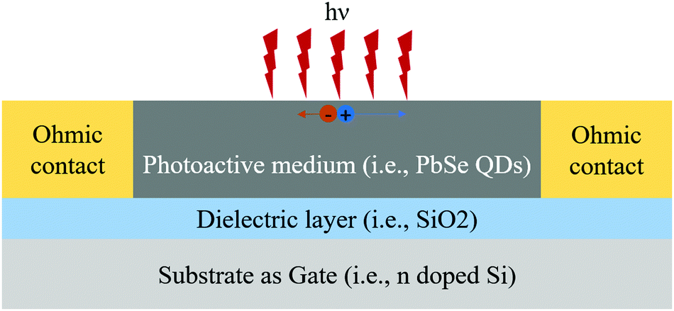
The IR imaging systems mainly use three types of basic device architecture, based on photoconductor, phototransistor, and photodiode. Different types of substrates for the detector development have been used, such as glass, Si, quartz, sapphire, GaAs, and transparent conductive oxides, but mostly glass and silicon are preferred based on cost.3 However, glass is not so well suited for MWIR range photodetection due to the lack of transparency. The choice of substrate depends on the type of structure and application. Different electrodes as ohmic contacts are being experimented for efficient generated carrier collection such as with their work function, silver (Ag, 4.7 eV),47,112 gold (Au, 5.1 eV),18,47,113,114 platinum (Pt, 6.35 eV),19,115 titanium (Ti, 4.33 eV),7,113,115 chromium (Cr, 4.5 eV),47,113 aluminium (Al, 4.2 eV),24,47 and graphene (∼4.56 eV).116,117 Choosing a proper electrode is a major concern for appropriate ohmic contact design while reducing the overall cost of the IR imaging devices. | ||
| Fig. 9 Device schematic of PbSe thin-film photodetector.121 (Reproduced from ref. 121 with permission of the Multidisciplinary Digital Publishing Institute, Nanomaterials). | ||
Photoconductor-based devices are generally used for IR applications such as imaging sensors and motion detection.121 Generally, the electrodes are placed on top of the film using a mask to create ohmic contacts and have the window for incident light absorption. Two ohmic contacts (considered as source and drain electrodes) are separated by a window known as the photoactive layer. The ohmic contact resistance is an essential parameter for the photo-sensing properties because the ratio of electrical resistance under illumination to dark conditions is maximized when the junction resistance is negligible.112 The device works under an applied bias voltage. The photoactive layer generates carriers (temporary changes in carrier density) under illumination, which are collected by the electrodes. The majority type of carriers has a shorter transit time than minority carriers and quickly traverse to an electrode, while the other electrode maintains the charge neutrality by providing additional carries, which defines the total gain.121
The responsivity of a detector depends on the amount of gain from the device. However, if the photodetector is limited by the noise then there is a possibility that the higher gain signals will also have higher noise levels. These kinds of photodetectors are not appropriate for highly sensitive applications. So, the design parameters should be optimized for high quantum efficiency and lower dark current.122
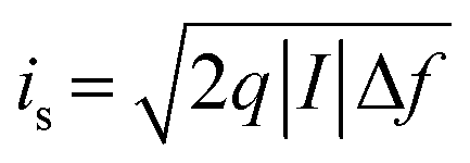
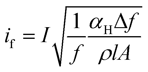
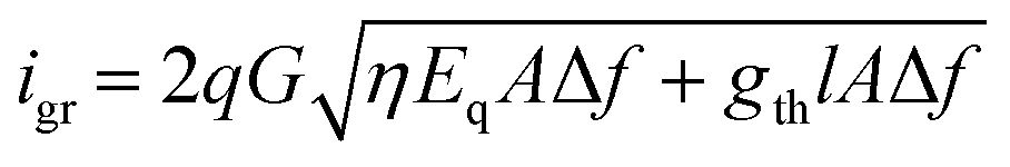
Generally, four types of noise mechanisms44 are considered for photodetector performance analysis, which are (1) thermal (Johnson–Nyquist) noise due to the carriers thermal agitation, (2) shot noise due to a finite number of carriers passing through the detector film, (3) flicker (1/f) noise due to an averaging effect of stochastic paths taken by the carriers through the transport, and (4) generation–recombination noise due to stochasticity of the generation–recombination (G–R) of carriers in the detector.
The Johnson noise current (ij),44,123 shot noise current (is),44,123 1/f noise current (if),44 and G–R noise current (igr)123 are given by the following equations, respectively.
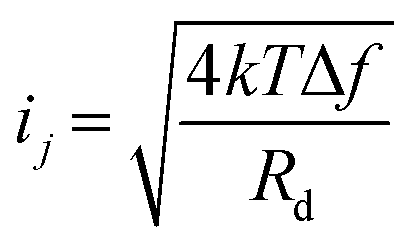 | (7) |
 | (8) |
 | (9) |
 | (10) |
So, the total noise current (in)123 can be expressed as the sum of the power of all noise sources, given in the following eqn (11).
| in2 = ij2 + is2 + if2 + igr2 | (11) |
For the last two decades, researchers are more focused on the QD form of PbSe for IR imaging devices. Because the PbSe QD can expand the range of current technologies and easily integrate with the complementary metal–oxide–semiconductor (CMOS) technology.121 However, ligands and dangling bonds on the surface of PbSe QDs work as barriers in charge transfer, which deteriorates the performance of the devices.114 The general device structure is the same as shown in Fig. 9, while the PbSe layer is developed using a QD form of the material, which is shown and discussed by Nakotte et al.121
 | ||
| Fig. 10 Schematic of a PbSe photoFET device structure.121 (Reproduced from ref. 121 with permission of the Multidisciplinary Digital Publishing Institute, Nanomaterials.) | ||
The modulation of drain–source current transport is controlled through the gate electrode by using an applied gate voltage.121 Charges are introduced into the conductive channel due to the applied gate voltage, which can be used to tune transport and control the total conductivity. For example, holes can be introduced by a negative applied bias to increase the conductivity of p-type lead chalcogenide QD films.121 Thus, the photoFETs architecture is more preferred for the QD-based detectors design to control the carrier modulation dynamics. For the same reason, the photoFETs design architecture is more effective than the photoconductors design.
The QD-based PbSe photoFETs with metallic (Au/Ag) nanowire transparent electrodes have been reported for the NIR regime applications with a high responsivity of 2 × 10⁴ A W−1 and a high specific D* of 7 × 10¹² Jones at low operation voltage (∼1 V).18
The D* of a photodiode can be defined by the following eqn (12).124 The D* indicates the signal to noise (S/N) ratio in an AC signal obtained from a detector to the input incident energy of 1 watt (W). The D* is normalized to the detector area of 1 cm2 and a noise bandwidth of 1 Hz, for easier comparison of different detectors.
 | (12) |
 | (13) |
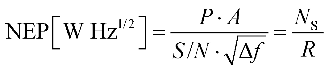
 comes from the total noise current eqn (11) and Rλ is the photoresponsivity at the peak wavelength λP.
Several papers calculated and reported D* for QD-based photodiode detectors by ignoring G–R noise, and sometimes even Johnson noise in MWIR. This could potentially lead to unrealistically high D*. Even though the G–R noise in high-quality monocrystalline photodiode can be ignored, but it should be considered for polycrystalline and nano-structured (QD, NW, etc.) films in which recombination at interfaces could be high.
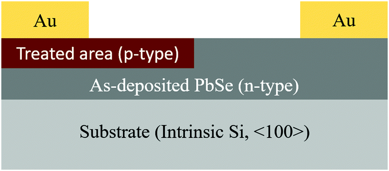
A photodiode device structure with a p–n junction is shown in Fig. 11, which is more like a planar architecture. A PbSe thin film (n-type) was deposited on top of an intrinsic Si wafer followed by a sensitization process to convert the top part of the thin film from n-type to p-type.114 Thus, it forms a p–n junction. Usually, in the photodiode, a moderate reverse bias is used to operate and create an effective depletion region, which results in a unity gain. However, under a large bias voltage, it can work in the avalanche mode and results in a gain higher than one.121 Applications necessitating fast response time usually use the photodiode configuration for detection.
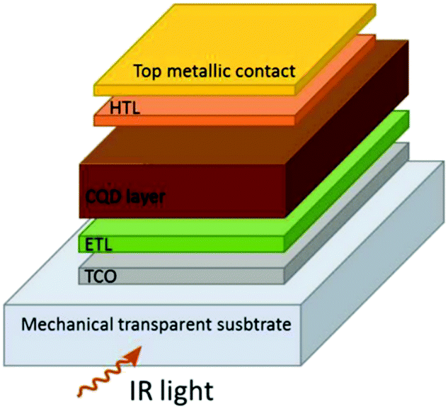 | ||
| Fig. 12 The general architecture of QD-based photodiode in vertical geometry.125 (Reproduced from ref. 125 with permission of the Frontiers in Chemistry, Nanoscience.) | ||
The most important gain of this structure is to utilize two separate layers for carrier transport (electron transport layer (ETL) and hole transport layer (HTL)). The key advantage of this configuration is that it induces an in-built electric field which makes the device operate nearly at zero volts biasing; thus, it can provide low dark current.125
A transparent conductive oxide (TCO) layer is deposited on top of the substrate. The conducting layers are indium tin oxide (ITO) and fluoride doped tin oxide (FTO).125 The ETL layer is deposited on top of the TCO layer and then annealed at high temperature; most widely used materials are inorganic layers made of ZnO or TiO2.125 The PbSe QD layer is deposited on top of the ETL layer with an average thickness of 200 to 400 nm considering the light absorption requirement, fabrication challenges, and transport diffusion length.125 The HTL layer is deposited on top of the QD layer; the most widely used material is MoO3.125 Finally, the metallic contact layer is deposited on top of the HTL layer. This general structure can also be applied with inverted geometry depending on the combination of the n- and p-type layers. At first, Chuang et al. reported a photovoltaic device architecture consisting of 10 layers of tetrabutylammonium (TABI)-capped PbS QDs and two layers of 1,2-ethanedithiol (EDT)-capped PbS QDs.126 Similarly, a double thin layer PbSe-EDT QDs, and PbSe-TABI QDs photodetector was fabricated by Zhu et al. for broadband applications.127 Interestingly, the QD-based photodetectors are commercially available (by SWIR Vision Systems). However, it is necessary to address the challenges such as material (synthesis and QD coupling), device (light–matter coupling, band alignment, noise, and responsivity), and camera integration (stability, FPA, pixel scaling, and hybrid fabrication with readout integrated circuit, ROIC).125
4.2 Advanced PbSe photodetector devices (state-of-the-art)
These various results of the fabrication of photodetectors were published in peer-reviewed journals. The reported figures of merit (R and D*) can vary significantly. While D* is intended to normalize the photoresponse for comparing many types of detectors, the method of determining D* is not trivial. It should also be noted that while many of the following photodetector devices, as fabricated, produce impressive figures of merit, the fabrication method and or device designs are not practical for practical applications. For instance, many of the active areas of these devices are covered by metal pads that are opaque to IR wavelengths. The illumination angle is limited to a very narrow range from an oblique angle.Hu et al. provided a thorough review of lead chalcogenide-based QD photodetectors and describes many important properties and characteristics as well as a description of the many types of photodetector configurations and synthesis methods.107 While much of the content of Hu's review is PbS-based, it provides a good overview of recent QD-based photodetectors beyond the scope of this review article.
The potential for broadband photodetectors using PbSe QDs is rapidly being realized due to the need for scientific, commercial, and industrial applications. Zhu et al. successfully produced a broadband PbSe QD-based photodetector with high photoresponsivity and detectivity from UV to MWIR (350–2500 nm).127 The group reportedly produced a multi-layer broadband photodetector that circumvented the low absorption coefficient of PbSe QDs by forming an n-type TBAI – (tetrabutylammonium iodide) capped layer of QDs on top of a p-type EDT (ethylene diamine tartrate (EDT)-capped PbSe QD layer. The group reported success in applying a hole-trap-assisted photomultiplication effect to boost the external quantum efficiency (EQE) ranging from NIR to MWIR.127 They reported an EQE of over 450% in the visible range and 120% in the NIR range.
Additionally, the group modified their ZnO electron extraction layer (EEL) used for suppressing the dark current by applying conjugated polyelectrolyte, which reduces hole transport in the dark but improves conductivity under illumination with photoinduced self-doping. They reported this dramatically improved the D* from the UV to the MWIR region. The group reported a D* of over 1012 Jones in the visible and 4 × 10¹¹ Jones in the MWIR region. It should be noted that the EDT and TBAI used for capping the PbSe QD are used in a ligand exchange process that removes the organic ligands. In the case of TBAI, the capping material is iodine-based (tetrabutylammonium iodide).
As mentioned in the MWIR section above, Qui et al. report a promising method of first achieving strong quantum confinement (blue-shift) properties with their ligand-free CBD process followed by a thermal anneal for fine-tuning the specific spectral response (red-shift).99 This group formed a PbSe-QD/CdS heterojunction allowing a photodetector tuning starting at visible with a potential range (red-shifting) back to MWIR (4.5 μm). With the growing demand for broadband IR photodetectors, the intermingling of multiple synthesis methods and materials will continue to stretch the capabilities of this rapidly growing technology. Hybrid films and stacked layers forming creative junctions and band alignment are sure to advance.
One type of IR photodiode detector was demonstrated by forming a p–n junction between PbSe and n-type metal oxides like ZnO or TiO2. The metal oxide layer acts as an electron-transporting layer, and the dark current of this configuration is reportedly two orders of magnitude lower than a Schottky-type photodiode.107 Sulaman et al. configured a PbS0.4Se0.6/ZnO(NP)/ITO photodiode and reported a D* of 1.3 × 10¹³ Jones129 illuminated under a 980 nm laser. The same group configured a broad IR photodiode by blending CH3NH3PbBr3 QDs with PbS0.4Se0.6 QDs and reported an equally impressive R of 21.48 A W−1 and a D* of 3.59 × 10¹³ Jones under 532 nm laser illumination and an R of 22.16 A W−1 and a D* of 3.70 × 10¹³ Jones under 980 nm laser illumination.107
Jiang et al. reported in 2015 the figure of merit performance of a tandem photodiode using a stack of glass/ITO/PEDOT:PSS/PbSe QDs/ZnO/(poly-TPD)/PbSe QDs/ZnO/Al. The group reported a D* of 4.7 × 10¹³ Jones at RT illuminated under an 1100 nm source of 34 mW cm−2. According to the group, this performance was achieved by addressing the dark current by introducing the intermediate Poly-TPD (poly(N,N′-bis-4-butylphenyl-N,N′-bisphenyl)benzidine) layer (IL), which fundamentally transitions the carrier transport mechanism from the previously dominant nearest-neighbor hopping (NNH) to recombination of carriers at the IL interface.130
Sulaman et al. reported a tandem broadband photodiode composed of a stack of ITO/PEDOT:PSS/CsPbBr3:PbS0.4Se0.6/ZnO/PVK/CsPbBr3:PbS0.4Se0.6/ZnO/Au with a maximum D* of 6.8 × 10¹³ Jones with an R of 27 A W−1 illuminated with a 980 nm wavelength using a 57.8 mW source.131 While this performance was impressive, it was further improved by introducing a 50 nm PMMA dielectric between the ZnO and PVK layers. This further enhanced the performance by increasing the maximum D* to 1.32 × 10¹⁴ Jones and an R of 27.72 A W−1 under the same illumination conditions.131 This research group explained that the presence of an appropriately thin dielectric layer of 50 nm of PMMA between the two sub-photodetectors acts as a trap-induced capacitor on either side of the PMMA, allowing holes and electrons to be repeatedly stored and extracted by the trap states. “The two interfaces play the role of ‘capacitor’ to cause the high photocurrent after re-setting applied voltage under illumination.”131 The group reports their enhanced tandem photodiode performance is above any previously reported traditionally inorganic or perovskites-based photodetectors.131
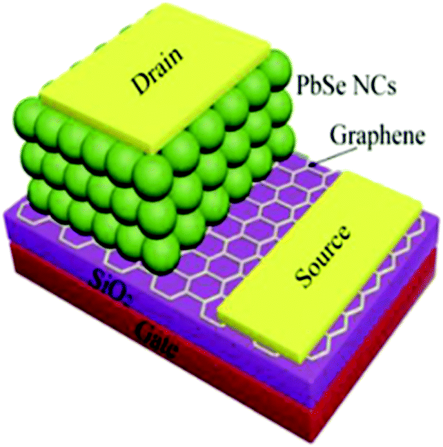
Che et al. produced a PbSe-based vertical phototransistor (VPT) with a graphene electrode.132 The group reports the Schottky barrier height between the graphene and the PbSe NCs can effectively modulate the carrier transport by utilizing the tuneable Fermi-energy properties of graphene.132 An illustration of the device can be seen in Fig. 13. Che reports a D* of 1.3 × 10¹⁰ Jones and an R of 1.1 × 10⁴ A W−1 illuminated under 36 mW cm−2.132 The group reported the measurements using a wavelength of 808 nm for absorption spectrum. It was not clear if they used 808 nm for the figure of merit measurements.
 | ||
| Fig. 13 Illustration and x-section of PbSe NC-based VPT.132 (Reproduced from ref. 132 with permission of the Elsevier, Optical Materials.) | ||
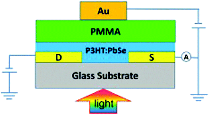
Wang et al. reported a successfully implemented vertical field-effect transistor (VFET) photodetector using an inverted design (compared to common gate orientation) with a solution-based PbSe QD fabrication. The group fabricated a device, as shown in Fig. 14, with an Au(Gate)/PMMA(930 nm)/P3HT:PbSe(55 nm)/Au (source, drain) configuration.133 The device performance was a D* of 5.02 × 10¹² Jones and an R of 500 A W−1 by illumination using a 980 nm laser with a 40 mW cm−2 and biased at VDS of −40 V and a VG = −40 V. The group reported that the inverted configuration is highly stable in air and further improvements will be realized by implementing a ligand exchange process.133
 | ||
| Fig. 14 Illustration and top-down of PbSe NC-based VFET.133 (Reproduced from ref. 133 with permission of the IEEE, Photonics Technology Letters.) | ||
Zhang et al. fabricated a traditionally oriented VFET using Au and Ag nanowires as a transparent source electrode (Fig. 15). By defining the channel length via the ultra-thin PbSe QD layer, (260 nm), superior photoconductive properties were observed, such as ambipolar operation at voltages as low as 1 V at RT.18 Their device D* and R reported as of 7 × 10¹² Jones and 2 × 10⁴ A W−1, respectively, and was illuminated with an 808 nm source with an irradiance of 1.25 mW cm−2.18 Liu et al. reported work that addresses progress on air-stabilized QD mobility by infilling their sulfide-capped PbSe QD films with ALD deposited amorphous alumina. They achieved a 7 cm2 V−1 s−1 electron mobility.34
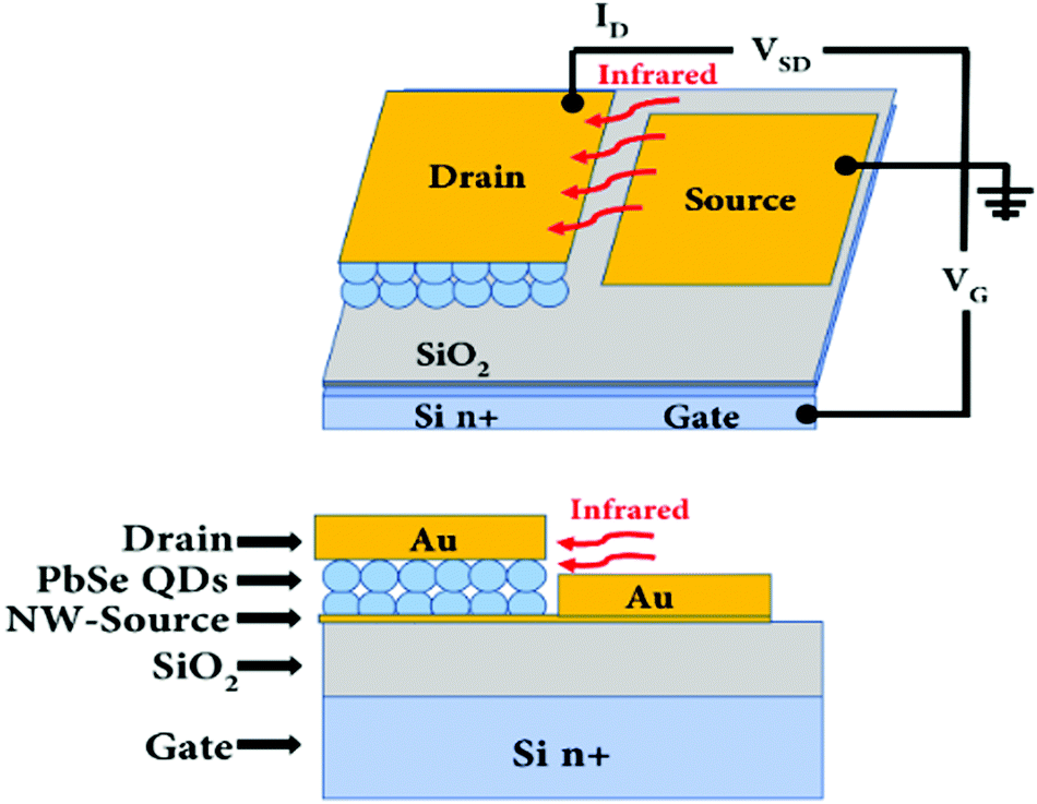 | ||
| Fig. 15 Illustration of top-down and cross-section of PbSe NC-based VFET.18 | ||
4.3 Focal plane array (FPA) structure
Irrespective of the design structures, the fabrication of the PbSe detectors in the FPA format is the key to many applications. Next, we examine the development of the general FPA format improved over time and the requirements for the current technology (Fig. 16), which is applicable for all IR imaging devices with different materials.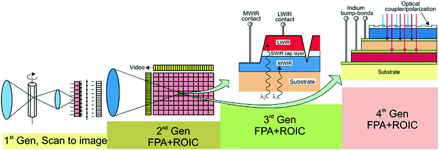 | ||
| Fig. 16 Four generations of IR detector systems that have evolved for all types of applications: first generation (scanning systems), second-generation (staring systems with electronic scanning), third-generation (staring systems with a large number of pixels and bi-color functionality), and fourth-generation (staring systems with a very large number of pixels, multi-color functionality, and other on-chip functions; e.g., better radiation/pixel coupling, avalanche multiplication in pixels, and polarization/phase sensitivity).134–136 (Reproduced from ref. 134 with permission of the AIP Publishing, Applied Physics Reviews.) | ||
The 1st generation was based on linear arrays of photoconductor without multiplexing functions. The 2nd was based on 2-D arrays of photodiodes with multiplexing on a focal plane silicon chip for electronic scanning of more than a megapixel of elements. The 3rd generation first added bi-color functionality by implementing two layers of thin-film to capture two different wavelength ranges simultaneously. This system is still evolving and improving while the 4th generation is already being introduced. However, the 4th generation is not well defined yet but expected to extract more information from a scanned system. It supports the largest number of pixels, higher frame rates, better thermal resolution, multicolor functionality, advanced color processing algorithms to further improve sensitivity, and other on-chip functions that require a high processing ROIC implementation in the device.134,135
Last few decades, IR imaging device fabrication is completely based on FPA, including the ROIC system, because FPA technology has revolutionized IR detection techniques. The functions of ROICs are pixel deselecting, antiblooming on each pixel, subframe imaging, output preamplifiers, and including yet other functions.4 The IR sensor chip is assembled by connecting 2-D arrays of detectors with indium bumps to an ROIC chip.
Two different architecture can be used for FPA fabrication, which is a hybrid and monolithic process. The hybrid technology is well established for other types of materials, especially cooled IR detectors, use this method.4 The monolithic technology is being researched for the uncooled PbSe FPA fabrication to reduce the fabrication costs and utilize the areas to their best. A well-organized FPA, including ROIC using monolithic fabrication technology, is shown in Fig. 17, fabricated using a wet chemical growth process. A continuous single or polycrystalline film is grown and then annealed for p–n junction development on a flat substrate, which already includes ROIC layout and works as a seed crystal as well as a mechanical support for the device.3
 | ||
| Fig. 17 Schematic of a p–n junction PbSe FPA monolithically integrated with ROIC by direct wet chemical growth.3 (Reproduced from ref. 3 with permission of the SPIE Digital Library, Proceedings of SPIE.) | ||
A monolithic photovoltaic Pb-salt based FPAs grown on Si substrates with integrated ROIC for MWIR range (3–5 μm) applications was developed by Zogg et al.137 The PbSe thermoelectrically cooled (TE-cooled) imaging sensor was developed on the ROIC substrate by Green et al. and has shown step by the step fabrication process.13 A low-cost 320 × 240 uncooled lead salt FPA camera was fabricated onto a CMOS multiplexer ROIC by Imager Litton Electro-Optical Systems.138 Keeping these structures in mind, the most challenging part is manufacturing the FPA with pixel downsizing and coupling to the ROIC.
The pixel size is an important parameter for FPA design. The pixel size of current IR technologies is limited to 10 to 50 μm because of the indium bump hybridization to the ROIC, which is highly complex for less than 10 μm pixel size.125 With the advancement of the QD materials processing, the FPA design challenges need to be addressed. The QD active layer can be directly deposited on a CMOS ROIC. However, developing homogeneous films while downsizing the pixel size and minimizing the pixel-to-pixel crosstalk could be a major issue. Interestingly, Arquer et al.139 have shown that the solution-processed QDs fabricated on top of the ROIC resulted in improved sensitivity and minimization of crosstalk. Another factor of necessary concern of the QD-based photodetectors is stability.
4.4 Solar cell applications
PbSe QDs are strong absorbers that can efficiently convert each incident photon into multiple excitons (carrier multiplication) with the photon energy higher than the bandgap of the QD, which led to the QD solar cell experiments.121 The large bulk exciton Bohr radius of PbSe creates strong quantum confinement in colloidal nanocrystals and allows bandgap and absorption edge tuning across the entire visible spectrum.24 Ma et al. fabricated a Schottky junction based PbSe QD solar cell on a glass substrate (Fig. 18) with ITO/PEDOT/PbSe/aluminum structure and reported efficiency of 4.57% with an open-circuit voltage (VOC) around 0.6 V.24 Zhu et al. used a SnO2 buffer layer to improve the performance and reported efficiency of 9.67% with VOC around 577.1 mV.25 Ahmad et al. reported the best PV device with the highest power conversion efficiency of 10.68%, fabricated using PbSe QD inks.26 Ma et al.24 also suggested that VOC can be increased by optimizing PbSe nanoparticle diameter, which eventually increases the overall efficiency. Also, photocurrent decreases with size because of the reduced absorption and increased recombination. Even though MEG leads to photovoltaic experiments, the MEG approach is not well suited for photon energy available in the solar spectrum. Also, the PbSe solar cell power conversion efficiency is limited by the poor air stability26,27 and low VOC due to the small bandgap24 of PbSe QDs and defects during film deposition.26 | ||
| Fig. 18 Schematic diagram of the Schottky junction-based PbSe solar cell.24 (Reproduced from ref. 24 with permission of the American Chemical Society, Nano.) | ||
The unique properties of PbSe QDs, such as tunable bandgap, easy surface modification, simple synthesis, and low-temperature solution processing, are the main reasons for a wide range of applications for various optoelectronic devices, including laser.115,140 SWIR to the visible integrated up-conversion imaging device is also proposed with a heterostructure where the PbSe nano-layer is used as an absorber.12
4.5 Enhancement of device performance
The performance of infrared photodetector (IRPD) devices can be increased by mainly two methods, which are by engineering the electronic properties of the absorbing material for improving detectivity (i.e., quantum efficiency) and by increasing the coupling of light to the electronic states of the absorbing material.1 The QD and semiconductor superlattice (SL) structures are being used to enhance the materials' quantum efficiency. New emerging nanostructures are being used to enhance the coupling of light with the IRPD, such as subwavelength structures (SWSs), antireflection (AR) coatings,8 nanoantenna surface plasmonic,6,141 photonic crystals (PCs), monolithic integrated PbSe with other materials,113 interference filters,113,142 and metamaterials.1 Moreover, the hybrid structure mostly provides better performance compared to a single structure, but it comes with higher costs and more fabrication complexity.143,144 Grayer et al.6 investigated and proposed a surface plasmonic structure shown in Fig. 19 to improve MWIR sensitivity and increase the operating temperature of PbSe photoconductive detectors.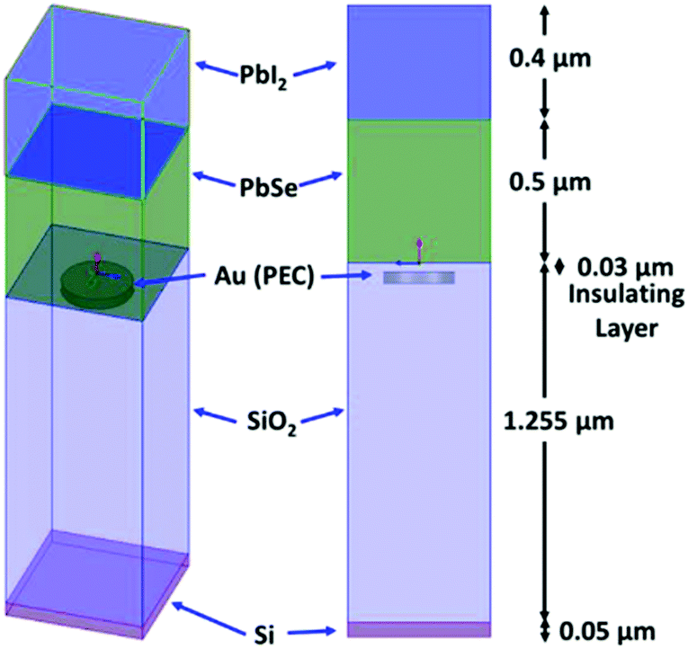 | ||
| Fig. 19 Schematic diagram of the proposed surface plasmon at the SiO2–PbSe interface.6 (Reproduced from ref. 6 with permission of the SPIE Digital Library, Proceedings of SPIE.) | ||
Unique electronic and optical properties can be achieved by fabricating the QD from the PbSe materials. Because of the zero dimensionality, QD-based IRPD devices can be fabricated at a lower cost, which offers higher QE than traditional IRPDs and operates at a higher temperature. In the last decade, the QD form is becoming more emerging for IRPD devices because of its quantum confinement characteristics. Most of the reported QD photoconductors work in the NIR to the MWIR regime and are based on the lead chalcogenide.1 Researcher has tried various ways to improve the overall efficiency of the IRPD devices.
4.6 Commercial devices
A list of uncooled PbSe commercial devices for MWIR imaging is shown in Table 6 with the device performances and parameters. These data are collected from the data sheets provided by the manufacturers. Even though the active area size (mm2) ranges from 1 × 1 mm2 to 10 × 10 mm2, for a good comparison, the device performances are noted for 2 × 2 mm2 devices. Most manufacturers mentioned the ranges of temperature for operation, but the performance decreases with increasing operating temperature. So, RT measurements are considered for comparison. A lot of companies have also fabricated cooled commercial devices with an extra layer for cooling to increase the sensitivity. However, this increases not only the cost of the device but also the complexity of the fabrication process.| Manufacturer | Detector size (mm2) | Spectral range (μm), peak (λp) | Operating temp. (K) | Dark res. (MΩ) | Detectivity, D* (p) (cm Hz1/2 W−1) | Peak sensitivity, ℜ(λ) (V W−1) |
|---|---|---|---|---|---|---|
| Thorlabs | 2 × 2 | 1.5 to 4.8 | 243 to 323 | 0.1–3.0 | 2.5 × 10⁹ | 1.5 × 10³ (Min.) |
| Peak at 4.0 | 3.0 × 10³ (Typ.) | |||||
| Hamamatsu | 2 × 2 to 3 × 3 | 1.5 to 4.8 | 243 to 323 | 0.3–1.5 | 8.0 × 10⁸ | 7.0 × 10² (Min.) |
| Peak at 4.3 | 1.0 × 10³ (Typ.) | |||||
| Laser Components | 1 × 1 to 6 × 6 | 1.0 to 4.7 | 208 to 363 | 0.1–2.5 | 1.8 × 10¹⁰ | 1.05 × 10⁴ (Min.) |
| Peak at 4.0 | 2.1 × 10⁴ (Typ.) | |||||
| AP Technologies | 1 × 1 to 6 × 6 | 1.0 to 5.0 | 233 to 358 | 0.5–2.5 | 2.0 × 10¹⁰ | 7.5 × 10³ (Min.) |
| Peak at 3.6 to 3.8 | ||||||
| 1.5 × 10⁴ (Typ.) | ||||||
| Teledyne Judson Tech. | 1 × 1 to 3 × 3 | 2.0 to 6.0 | 208 to 298 | 0.1–2.0 | 5.0 × 10⁹ | 7.5 × 10³ (Min.) |
| Peak at 3.8–4.0 | 2.1 × 10⁴ (Typ.) | |||||
| EOC Inc. | 1 × 1 to 10 × 10 | 2.0 to 6.0 | 208 to 298 | 0.1–4.0 | 1.5 × 10¹⁰ | 5.0 × 10³ (Min.) |
| Peak at 3.8 | 2.0 × 10⁴ (Typ.) | |||||
| New England Photoconductor | 1 × 1 to 10 × 10 | Peak at 3.8 | 208 to 298 | 0.1–4.0 | 1.5 × 10¹⁰ | 5.0 × 10³ (Min.) |
| 2.0 × 10⁴ (Typ.) | ||||||
| Opto Diode Corporation | 1 × 1 to 6 × 6 | 1.0 to 5.0 | 233 to 358 | 0.5–2.5 | 2.0 × 10¹⁰ | 7.5 × 10³ (Min.) |
| Peak at 3.6 to 3.8 | 1.5 × 10⁴ (Typ.) | |||||
| Infrared Materials, Inc. | 1 × 1 to 10 × 10 | 1.0 to 5.5 | 233 to 358 | 0.1–3.5 | 1.8 × 10¹⁰ | 1.12 × 10⁴ (Min.) |
| Peak at 3.8 | 2.25 × 10⁴ (Typ.) | |||||
| EOS Inc. | 1 × 1 to 5 × 5 | 1.0 to 4.5 | 243 to 295 | 0.2–1.0 | 5.0 × 10⁹ | 4.0 × 10³ (Min.) |
| Peak at 3.8 | ||||||
| TrinamiX GmbH | Multi-pixel | 1.0 to 5.0 | 243 to 343 | 0.3–20 | 1.8 × 10¹⁰ | 1.12 × 10⁴ (Min.) |
| Peak at 3.8 | 2.25 × 10⁴ (Typ.) | |||||
| New Infrared Technologies | 1 × 1 to 2 × 2 | 1.0 to 5.0 | 233 to 358 | 0.8–1.0 | 2.0 × 10⁹ | 1.12 × 10⁴ (Min.) |
| Peak at 3.7 | 4.5 × 10³ (Typ.) | |||||
| Agiltron Inc. | 1 × 1 to 6 × 6 | 2.0 to 5.0 | 298 | 0.2–5.0 | 2.0 × 10⁹ | 7.5 × 10³ (Typ.) |
5. Alternative approaches for IR detectors
Recently IR detector based on germanium tin or silicon germanium tin (GeSn/SiGeSn) alloy and 2D materials are being researched and used for imaging application ranging from SWIR to MWIR. When so-called α-Sn (gray tin) is incorporated into Ge with a ratio of 10% and below, the alloy transforms from indirect bandgap to direct bandgap,145 and it lowers the absorption edges of Ge. The Ge1−ySny layer in both GeSn binary and SiGeSn ternary alloy has some unique properties145–147 for photodetection applications such as (i) strain-relaxed and low threading-defect densities (105 cm−2) (for <1 μm in thickness), (ii) low growth temperatures (250 to 350 °C) and thermal stability for conventional semiconductor processing (up to 750 °C), (iii) tuneable bandgap (0.5 to 0.8 eV) and tuneable lattice constants (5.65 to 5.8 Å), (iv) extremely flat surface, (v) selective growth on Si and Ge substrate, (vi) film surface preparation by simple chemical cleaning for subsequent ex situ epitaxy, (vii) CMOS compatible and suitable for large-scale and low-cost integration, and (viii) low-power operation. However, there is a huge fabrication challenge for both GeSn binary and SiGeSn ternary alloy due to the very low solubility145 of α-Sn in Ge and Si. Despite the fabrication challenges, the GeSn/SiGeSn alloy is a promising material for future photodetector applications due to its outstanding characteristics. Some of the common applications147 of the GeSn/SiGeSn thin films are photodetectors, photovoltaics, laser diodes, IR amplifiers, electro-optical modulators, and electro-optical (EO) routing switches.Table 7 summarizes recent photodetectors development based on GeSn and SiGeSn alloy by using mostly CVD and MBE fabrication processes. Other fabrications methods have also been experimented with, such as solid phase epitaxy (SPE), sputtering, and PLD.148–151 The device structure follows mostly p–i–n configuration with the highest D*152 of 4.6 × 109 cm Hz1/2 W−1 and highest responsivity146 of 2.85 A W−1 at 1.55 μm wavelength. However, most of the research is focused on GeSn photodetectors due to the fabrication complexity of SiGeSn ternary alloy. Both single crystalline153–155 and polycrystalline156–158 GeSn thin films are reported for photodetection with the absorption coefficient of the polycrystalline form is higher than the single crystalline due to the scattering effect at the grain boundaries. However, the electrical resistivity of the polycrystalline form could be lower than the single crystalline form because the grain boundaries generate holes in Ge-based semiconductors.
| Type | Structure | Fabrication process | E g (eV) | Thick. (nm) | Sn (%) | IR range (μm) | Temp. (K) | Detectivity, D* (cm Hz1/2 W−1) | Responsivity (A W−1) at λp |
|---|---|---|---|---|---|---|---|---|---|
| Alloy146 | p–i–n (GeSn) | CVD | 95 | 10.0 | 1.55 | 77 | 4.0 × 10⁹ | 2.85 at 1.55 | |
| 300 | 0.26 at 1.55 | ||||||||
| Alloy165 | p–i–n (GeSn) | MBE | 300 | 4.0 | 1.2–2.0 | 300 | 0.181 at 1.55 | ||
| Alloy166 | p–i–n (GeSn) | MBE | 200 | 1.3, 2.7 | 1.2–1.7 | 300 | 0.1 at 1.55 | ||
| Alloy167 | p–i–n (GeSn) | MBE | 0.71 | 820 | 3.0 | 0.8–1.8 | 300 | 0.52, 0.23, 0.12 at 1.31, 1.54, 1.64 | |
| Alloy168 | p–i–n (GeSn) | MBE | 0.64 | 300 | 0.5 | 1.23–1.7 | 300 | 0.1 at 1.55 | |
| Alloy169 | p–i–n (GeSn) | MBE | 0.8 | 300 | 4.2 | 1.55 | 300 | 0.218 at 1.55 | |
| Alloy170 | p–i–n (GeSn) | CVD | 0.54 | 200 | 7.0 | Up to 2.2 | 77 | 4.0 × 10⁹ at 1.55 | 0.3 at 1.55 |
| 0.52 | 200 | 10.0 | Up to 2.6 | 300 | |||||
| Alloy171 single (QW) | p–i–n (GeSn) | CVD | 0.57 | 20 | 9.0 | 0.75–2.4 | 300 | 0.1 | |
| Alloy172 (multi-QW) | p–i–n (GeSn) | MBE | 0.56 | 10 × 15 | 10.0 | 1.53–2.0 | 300 | 0.216 at 1.53 | |
| 0.023 at 2.0 | |||||||||
| Alloy152 (single layer) | p–i–n (GeSn) | CVD | 95 | 10.0 | Up to 2.2 | 77 | 4.6 × 10⁹ at 1.55 | 1.63 at 1.55 | |
| Up to 2.4 | 300 | ||||||||
| Alloy173 (multi-QW) | p–i–n (SiGeSn) | Lithographic process | 0.76 | 4 × 10 | 6.5, 11.4 | 1.24–1.9 | 300 | 0.049 at 1.25 | |
| Alloy174 (multi-QW) | p–i–n (SiGeSn) | MBE | 6–10 | 7.1 | 1.55 | 300 | 0.17 at 1.55 | ||
| Alloy175 | p–i–n (SiGeSn) | CVD + MBE | 0.7 | 500–1000 | 1.2–5 | 1.15–1.45 | 300 | 0.15–0.36 |
Various 2D materials, including graphene, transition metal dichalcogenides (TMDs), hexagonal boron nitride (hBN), and black phosphorus (BP), have been researched for various photonics and optoelectronics applications focusing on mid-infrared photodetectors.159,160 The 2D materials offer some unique advantages such as MIR bandgaps, small size, high carrier mobility, easy integration, ultrafast photoresponse, and broadband absorption.159,160 It can be designed to a single (atomic level) or a few layers, which are mechanically robust and naturally passivated on the surface. Thus, it can be integrated into other structures without worrying about the lattice mismatch issue that usually happens in bulk materials.159 Both electronic structure and optical properties of the 2D materials are controllable, considered promising candidates for MIR integrated photonics.
Graphene is the first single-layered material discovered, which exhibits excellent electron mobility at RT.159 Unlike graphene, some indirect bandgap semiconductor materials of the TMD family (MoS2, WS2, MoSe2, and WSe2) exhibit direct bandgap (1.57 to 2.0 eV) when thinned down to a single layer, which enables stronger photoluminescence.159 Some noble metal TMDs, such as PtS2, PtSe2, PdS2, and PdSe2, are also being investigated for MIR detectors due to their suitable MIR bandgaps and high environmental stability.159 The puckered (honeycomb) structure of monolayer BP leads to anisotropic physical properties, which results in anisotropic optical absorption and photoluminescence.159 This unique structure enables BP for monolithic integration with traditional CMOS technology (silicon) and the possibility of placing on different substrates. All these 2D materials can be tuned to MIR bandgap ranges with controlling doping and defect. The 2D materials can be configured into heterostructures even with different types of material by using the van der Waals force. Many 2D heterostructures (graphene-hBN, graphene-BP, TMD-hBN, and TMD-graphene) have been proposed with wide-ranging electronic and optical properties.
Current commercial photodetectors have the limitations of operating at low temperatures to avoid high dark current or require a cooling process to operate at higher temperatures. The 2D materials can be used to overcome this challenge for MIR photodetectors. Fang et al.159 and long et al.160 summarized the performances (spectrum range, responsivity, response time, and detectivity) of a list of MIR photodetectors based on the 2D-materials and their heterostructures. Most of these reported studies were mainly focused on graphene, BP, and heterostructures. For the MIR region, the maximum reported photo responsivity is around 82 A W−1 for a BP 2D material, whereas the highest D* is around 4.9 × 10⁹ Jones for a b-AsP-MoS2 heterostructure. Long et al.160 compared the traditional photodetectors with 2D-based photodetectors based on operating temperature, spectral range, and bandgap values.
The present and future research efforts of IR technology should be focused on lowering the system's cost by reducing device size, weight, and power consumption (SWaP). The ultimate target is to fabricate a high operating temperature (HOT) photodetector for FPA applications, characterized by high quantum efficiency and dark current lower than the shot noise from system background flux current and the flicker (1/f) noise.122 The PbSe based photodetectors offer a promising solution to address these challenges.
Among group II–VI, the HgCdTe (MCT) thin film is a premium material for high-performance photodetectors in the NIR-LWIR range due to its tunable bandgap over a wide spectral range, high absorption coefficient, high carrier mobility, and long carrier lifetime.161–163 However, it has some major drawbacks such as the most expensive material, FPA integration with SOIC due to large lattice mismatch with Si, requires cryogenic cooling leads to a bulky system, low dark current density, and requires advanced plasma dry etching technology leads to severe manufacturing costs.122,161,163,164 High carrier lifetimes lead to a high gain but reduce quantum efficiency.161 It has deficient performance at higher operating temperatures due to a high Auger recombination rate, which leads to increased loss, otherwise known as Auger theoretical limit.162
Recently, new improvements are reported to fabricate FPA by using MCT QDs for infrared photodetection. MCT QD-based photodetectors could be a potential candidate due to their negative bandgap Eg = −0.15 eV and large Excitonic Bohr radius, which ensures the quantum confinement effect at the desired spectral range.176,177 Chatterje et al. reported MCT-based FPA by drop-casting synthesized QD over Si ROIC to evaluate low176 temperature response and shockwave dispersion technique for RT177 response.
Some groups also reported that HgTe QD is a good choice for MWIR to LWIR infrared imaging because it exhibits optical gaps larger than the bulk HgTe. Buurma et al.178 demonstrated MWIR thermal imaging photoconductive HgTe CQD films, which were drop cast on a commercial silicon ROIC chip. Also, Keuleyan et al.179 reported HgTe QD MWIR photodetectors with an RT photoresponse even beyond 5 μm.
Among group III–V, the InGaAs and InSb are the most appropriate materials for NIR-SWIR range photodetectors.161 The drawbacks of these materials are not enough photoresponse in the MWIR range, expensive material, difficulty of FPA integration, CMOS incompatibility with ROIC, high manufacturing cost, and low thermal reliability.161,180 The GeSn based photodetector is a promising research focus for future applications due to its outstanding characteristics in the NIR-SWIR range, including CMOS compatibility. However, it has some significant drawbacks such as not enough photoresponse in the MWIR range, surface segregation, precipitations, defect accumulation in low-temperature epitaxy, high fabrication cost, and high lattice mismatch between Si and GeSn (>4%), which requires an additional Ge buffer layer leading to fabrication complexity.181
Even though 2D materials and their heterostructures are promising for future MWIR photodetectors, still its performance is lower than traditional detectors on the global market (i.e., PbSe, InGaAs, and HgCdTe) due to the infancy stage of technology.122 It also suffers from slow photodetection speed, shot noise limit, and flicker noise.161 Intensive research is needed to understand the controlling defects, the impact of substrate, impurity, and theoretical model to control both electronic and optical properties. Also, an investigation is required on novel fabrication processes to integrate IR detectors into the photonic integrated chip for further advancement, including precise and large-scale assembly of 2D materials. Another challenge is to fabricate 2D materials into the FPA form, which is barely investigated.
The photoconductive PbSe thin film can outperform its competing materials, especially considering the HOT photodetectors, applicable IR range (NIR-MWIR), and FPA integration with CMOS technology. Some challenges need to be addressed first, which are significant flicker noise, poor long-term stability, bad photoresponse uniformity, high dielectric constant, and understanding the physics behind the activation of the film.142 Northrop Grumman reported monolithic PbSe detector integrated FPA with Si ROIC including thermoelectric cooling for photonic and uncooled IR imaging applications.162
The Centro de Investigación y Desarrollo de la Armada (CIDA) reported an innovative technology for processing polycrystalline PbSe thin film which offers good reproducibility, good uniformities, long term stability, plain Si substrates (no textured) compatibility, compatibility with existing Si CMOS technology, simple and affordable, compatible with complex multilayer structures (interference filters), and imaging device monolithically integrated with ROIC for FPA imaging.142 The PbSe materials limitation such as flicker noise and high dielectric constant can be minimized by using a specific ROIC and the processing capabilities of advanced nanoelectronics.
6. Conclusion
The PbSe thin film focal plane arrays play an essential role for imaging in the spectral range of 1 to 5 microns. Sensitization is a critical step to achieve high IR sensitivity, but a fundamental understanding of the mechanism is still lacking. This review provides state-of-the-art PbSe thin film work for IR imaging, including quantum dots. We have discussed the various methods for thin-film fabrication, IR detection, device designs, and applications. With recent progress in PbSe QD-based thin films and devices, this material continues to play an important role in IR imaging applications. Some of the challenges include lowering noise for RT operation, integration with silicon electronics, fundamental understanding of detection mechanism, and long-term stability.Author contributions
Mool C. Gupta: conceptualization, funding acquisition, project administration, resources, supervision, writing – review and editing. Joel T. Harrison: data curation, investigation, validation, formal analysis, visualization, writing – original draft, writing – review and editing. Md Toriqul Islam: data curation, investigation, validation, formal analysis, visualization, writing – original draft, writing – review and editing.Conflicts of interest
There are no conflicts of interest to declare.Acknowledgements
We acknowledge the support from the NIA Langley professor Program and NSF IUCRC Center.References
- C. L. Tan and H. Mohseni, Emerging technologies for high performance infrared detectors, Nanophotonics, 2018, 7, 169–197 Search PubMed.
- A. Karim and J. Y. Andersson, Infrared detectors: Advances, challenges and new technologies, IOP Conf. Ser.: Mater. Sci. Eng., 2013, 51, 12001 CrossRef CAS.
- B. Weng, J. Qiu, L. Zhao, Z. Yuan, C. Chang and Z. Shi, Recent development on the uncooled mid-infrared PbSe detectors with high detectivity, Quantum Sens. Nanophoton. Devices XI, 2013, 8993, 899311 CrossRef.
- A. Rogalski, History of infrared detectors, Opto-Electron. Rev., 2012, 20, 279–308 Search PubMed.
- Y. X. Ren, T. J. Dai, W. B. Luo and X. Z. Liu, Evidences of sensitization mechanism for PbSe thin films photoconductor, Vacuum, 2018, 149, 190–194 CrossRef CAS.
- J. S. Grayer, S. Ganguly and S.-S. Yoo, Embedded surface plasmon resonant disc arrays for improved MWIR sensitivity and increased operating temperature of PbSe photoconductive detectors, SPIE Digital Library, Proceedings of SPIE, 2019, 11082, 81 Search PubMed.
- V. Kasiyan, Z. Dashevsky, C. Minna Schwarz, M. Shatkhin, E. Flitsiyan, L. Chernyak and D. Khokhlov, Infrared detectors based on semiconductor p–n junction of PbSe, J. Appl. Phys., 2012, 112(8), 086101 CrossRef.
- B. Weng, J. Qiu, Z. Yuan, P. R. Larson, G. W. Strout and Z. Shi, Responsivity enhancement of mid-infrared PbSe detectors using CaF2 nano-structured antireflective coatings, Appl. Phys. Lett., 2014, 104(2), 021109 CrossRef.
- J. Qiu, B. Weng, Z. Yuan and Z. Shi, Study of sensitization process on mid-infrared uncooled PbSe photoconductive detectors leads to high detectivity, J. Appl. Phys., 2013, 113(10), 103102 CrossRef.
- Z. Dashevsky, V. Kasiyan, G. Radovsky, E. Shufer and M. Auslender, Sixth International Conference on Advanced Optical Materials and Devices (AOMD-6), 2008, 7142, 71420L-71420L-12.
- Z. Feit, J. Fuchs, D. Kostyk and W. Jalenak, Liquid phase epitaxy grown PbSnSeTe/PbSe double heterostructure diode lasers, Infrared Phys. Technol., 1996, 37, 439–443 CrossRef CAS.
- G. Sarusi, T. Templeman, E. Hechster, N. Nissim, V. Vitenberg, N. Maman, A. Tal, A. Solodar, G. Makov, I. Abdulhalim, I. Visoly-Fisher and Y. Golan, Nanophotonics VI, 2016, p. 9884 Search PubMed.
- K. Green, S.-S. Yoo and C. Kauffman, Infrared Technology and Applications XL, 2014, vol. 9070, p. 90701G Search PubMed.
- J. M. Martin, J. L. Hernández, L. Adell, A. Rodriguez and F. López, Arrays of thermally evaporated PbSe infrared photodetectors deposited on Si substrates operating at room temperature, Semicond. Sci. Technol., 1996, 11, 1740–1744 CrossRef CAS.
- A. Muñoz, J. Meléndez, M. C. Torquemada, M. T. Rodrigo, J. Cebrián, A. J. De Castro, J. Meneses, M. Ugarte, F. López, G. Vergara, J. L. Hernández, J. M. Martín, L. Adell and M. T. Montojo, PbSe photodetector arrays for IR sensors, Thin Solid Films, 1998, 317, 425–428 CrossRef.
- M. T. Rodrigo, F. J. Sánchez, M. C. Torquemada, V. Villamayor, G. Vergara, M. Verdú, L. J. Gómez, J. Diezhandino, R. Almazán, P. Rodríguez, J. Plaza, I. Catalán and M. T. Montojo, Polycrystalline lead selenide x–y addressed uncooled focal plane arrays, Infrared Phys. Technol., 2003, 44, 281–287 CrossRef CAS.
- T. Namitha Asokan, K. S. Urmila and B. Pradeep, Structural, optical, transient photoconductivity studies and low temperature thermoelectric power measurements on reactively evaporated lead selenide thin films, J. Mater. Sci.: Mater. Electron., 2016, 27, 5646–5653 CrossRef CAS.
- H. Zhang, Y. Zhang, X. Song, Y. Yu, M. Cao, Y. Che, J. Wang, J. Yang, H. Dai, G. Zhang and J. Yao, High performance PbSe colloidal quantum dot vertical field effect phototransistors, Nanotechnology, 2016, 27(42), 425204 CrossRef PubMed.
- M. Thambidurai, Y. Jang, A. Shapiro, G. Yuan, H. Xiaonan, Y. Xuechao, Q. J. Wang, E. Lifshitz, H. V. Demir and C. Dang, High performance infrared photodetectors up to 28 μm wavelength based on lead selenide colloidal quantum dots, Opt. Mater. Express, 2017, 7, 2326–2335 CrossRef CAS.
- M. Sulaman, S. Yang, A. Bukhtiar, C. Fu, T. Song, H. Wang, Y. Wang, H. Bo, Y. Tang and B. Zou, High performance solution-processed infrared photodetector based on PbSe quantum dots doped with low carrier mobility polymer poly(N-vinylcarbazole), RSC Adv., 2016, 6, 44514–44521 RSC.
- J. Gao, S. C. Nguyen, N. D. Bronstein and A. P. Alivisatos, Solution-processed, high-speed, and high-quantum-efficiency quantum dot infrared photodetectors, ACS Photonics, 2016, 3, 1217–1222 CrossRef CAS.
- Z. Zhang, J. Yang, X. Wen, L. Yuan, S. Shrestha, J. A. Stride, G. J. Conibeer, R. J. Patterson and S. Huang, Effect of halide treatments on PbSe quantum dot thin films: Stability, hot carrier lifetime, and application to photovoltaics, J. Phys. Chem. C, 2015, 119, 24149–24155 CrossRef CAS.
- J. J. Choi, Y. F. Lim, M. K. E. B. Santiago-Berrios, M. Oh, B. R. Hyun, L. Sun, A. C. Bartnik, A. Goedhart, G. G. Malliaras, H. D. Abruña, F. W. Wise and T. Hanrath, PbSe nanocrystal excitonic solar cells, Nano Lett., 2009, 9, 3749–3755 CrossRef CAS PubMed.
- W. Ma, S. L. Swisher, T. Ewers, J. Engel, V. E. Ferry, H. A. Atwater and A. P. Alivisatos, Photovoltaic performance of ultrasmall PbSe quantum dots, ACS Nano, 2011, 5, 8140–8147 CrossRef CAS PubMed.
- M. Zhu, X. Liu, S. Liu, C. Chen, J. He, W. Liu, J. Yang, L. Gao, G. Niu, J. Tang and J. Zhang, Efficient PbSe colloidal quantum dot solar cells using SnO2 as a buffer layer, ACS Appl. Mater. Interfaces, 2020, 12, 2566–2571 CrossRef CAS PubMed.
- W. Ahmad, J. He, Z. Liu, K. Xu, Z. Chen, X. Yang, D. Li, Y. Xia, J. Zhang and C. Chen, Lead selenide (PbSe) colloidal quantum dot solar cells with >10% efficiency, Adv. Mater., 2019, 31, 593 Search PubMed.
- J. Zhang, J. Gao, C. P. Church, E. M. Miller, J. M. Luther, V. I. Klimov and M. C. Beard, PbSe quantum dot solar cells with more than 6% efficiency fabricated in ambient atmosphere, Nano Lett., 2014, 14, 6010–6015 CrossRef CAS PubMed.
- L. Hu, Z. Zhang, R. J. Patterson, S. B. Shivarudraiah, Z. Zhou, M. Ng, S. Huang and J. E. Halpert, PbSe quantum dot passivated via mixed halide perovskite nanocrystals for solar cells with over 9% efficiency, Sol. RRL, 2018, 2(12), 1800234 CrossRef.
- J. S. Steckel, S. Coe-Sullivan, V. Bulović and M. G. Bawendi, 1.3 μm to 1.55 μm tunable electroluminescence from PbSe quantum dots embedded within an organic device, Adv. Mater., 2003, 15, 1862–1866 CrossRef CAS.
- W. Liang, A. I. Hochbaum, M. Fardy, O. Rabin, M. Zhang and P. Yang, Field-effect modulation of seebeck coefficient in single PbSe nanowires, Nano Lett., 2009, 9, 1689–1693 CrossRef CAS PubMed.
- W. Liang, O. Rabin, A. I. Hochbaum, M. Fardy, M. Zhang and P. Yang, Thermoelectric properties of p-type PbSe nanowires, Nano Res., 2009, 2, 394–399 CrossRef CAS.
- B. Weng, J. Ma, L. Wei, L. Li, J. Qiu, J. Xu and Z. Shi, Room temperature mid-infrared surface-emitting photonic crystal laser on silicon, Appl. Phys. Lett., 2011, 99(22), 221110 CrossRef.
- S. J. Oh, D. K. Kim and C. E. R. Kagan, Remote doping and Schottky barrier formation in strongly quantum confined single PbSe nanowire field-effect transistors, ACS Nano, 2012, 6, 4328–4334 CrossRef CAS PubMed.
- Y. Liu, J. Tolentino, M. Gibbs, R. Ihly, C. L. Perkins, Y. Liu, N. Crawford, J. C. Hemminger and M. Law, PbSe quantum dot field-effect transistors with air-stable electron mobilities above 7 cm2 V−1 s−1, Nano Lett., 2013, 13, 1578–1587 CrossRef CAS PubMed.
- R. Graham and D. Yu, High carrier mobility in single ultrathin colloidal lead selenide nanowire field effect transistors, Nano Lett., 2012, 12, 4360–4365 CrossRef CAS PubMed.
- Brian Elias, Recent Developments in Photoconductive Infrared Arrays, Recent Developments in Photoconductive Infrared Arrays, in SENSOR + TEST Conferences, 2009, vol. 1, pp. 243–248.
- S. L. Elizondo, F. Zhao, J. Kar, J. Ma, J. Smart, D. Li, S. Mukherjee and Z. Shi, Dielectric charge screening of dislocations and ionized impurities in PbSe and MCT, J. Electron. Mater., 2008, 37, 1411–1414 CrossRef CAS.
- X. B. Li, P. Guo, Y. N. Zhang, R. F. Peng, H. Zhang and L. M. Liu, High carrier mobility of few-layer PbX (X = S, Se, Te), J. Mater. Chem. C, 2015, 3, 6284–6290 RSC.
- S. J. Oh, C. Uswachoke, T. Zhao, J. H. Choi, B. T. Diroll, C. B. Murray and C. R. Kagan, Selective p- and n-doping of colloidal PbSe nanowires to construct electronic and optoelectronic devices, ACS Nano, 2015, 9, 7536–7544 CrossRef CAS PubMed.
- F. Briones, D. Golmayo and C. Ortiz, The role of oxygen in the sensitization of photoconductive PbSe films, Thin Solid Films, 1981, 78, 385–395 CrossRef CAS.
- D. Li, J. Ma, S. Mukherjee, G. Bi, F. Zhao, S. L. Elizondo and Z. Shi, A new in situ surface treatment during MBE-grown PbSe on CaF2/Si(111) heterostructure, J. Cryst. Growth, 2009, 311, 3395–3398 CrossRef CAS.
- F. Zhao, J. Ma, D. Li, S. Mukherjee, G. Bi and Z. Shi, Influence of oxygen post-growth annealing on optical and electrical properties of PbSe thin films, J. Electron. Mater., 2009, 38, 1661–1665 CrossRef CAS.
- V. V. Tetyorkin, A. Y. Sipatov, F. F. Sizov, A. I. Fedorenko and A. Fedorov, (001)-Oriented lead selenide films grown on silicon substrates, Infrared Phys. Technol., 1996, 37, 379–384 CrossRef CAS.
- S. Ganguly, M. H. Jang, Y. Tan, S. S. Yoo, M. C. Gupta and A. W. Ghosh, A multiscale materials-to-systems modeling of polycrystalline PbSe photodetectors, J. Appl. Phys., 2019, 126(14), 143103 CrossRef.
- M. H. Jang, S. S. Yoo, M. T. Kramer, N. K. Dhar and M. C. Gupta, Electrical transport properties of sensitized PbSe thin films for IR imaging sensors, Semicond. Sci. Technol., 2019, 34(6), 065009 CrossRef CAS.
- H. Yang, G. Wang, X. Li and J. Zheng, A nano-structured PbSe polycrystalline material prepared by ion beam implantation: Properties and comparison with the diffusion counterpart, J. Alloys Compd., 2019, 786, 449–456 CrossRef CAS.
- S. J. Oh, Designing Nanomaterials For Electronic And Optoelectronic Devices Through Charge Carrier Control, University of Pennsylvania, 2014 Search PubMed.
- J. N. Humphrey and R. L. Petritz, Photoconductivity of lead selenide: Theory of the mechanism of sensitization, Phys. Rev., 1957, 105, 1736–1740 CrossRef CAS.
- J. N. Humphrey and W. W. Scanlon, Photoconductivity in lead selenide, Exp. Phys. Rev., 1957, 105, 469–476 CrossRef CAS.
- L. Zhao, J. Qiu, B. Weng, C. Chang, Z. Yuan and Z. Shi, Understanding sensitization behavior of lead selenide photoconductive detectors by charge separation model, J. Appl. Phys., 2014, 115(8), 084502 CrossRef.
- X. Sun, K. Gao, X. Pang, H. Yang and A. A. Volinsky, Structure and composition effects on electrical and optical properties of sputtered PbSe thin films, Thin Solid Films, 2015, 592, 59–68 CrossRef CAS.
- T. N. Otto and D. Yu, Positive temperature coefficient of resistance and bistable conduction in lead selenide quantum dot thin films, J. Phys. Chem. C, 2013, 117, 3713–3717 CrossRef CAS.
- B. L. Wehrenberg, D. Yu, J. Ma and P. Guyot-Sionnest, Conduction in charged PbSe nanocrystal films, J. Phys. Chem. B, 2005, 109, 20192–20199 CrossRef CAS PubMed.
- T. S. Mentzel, V. J. Porter, S. Geyer, K. MacLean, M. G. Bawendi and M. A. Kastner, Charge transport in PbSe nanocrystal arrays, Phys. Rev. B: Condens. Matter Mater. Phys., 2008, 77, 7 CrossRef.
- M. Shandalov and Y. Golan, Microstructure and morphology evolution in chemical solution deposited semiconductor films: 2. PbSe on as face of GaAs(111), EPJ Appl. Phys., 2004, 28, 51–57 CrossRef CAS.
- J. E. Murphy, M. C. Beard, A. G. Norman, S. P. Ahrenkiel, J. C. Johnson, P. Yu, O. I. Mićić, R. J. Ellingson and A. J. Nozik, PbTe colloidal nanocrystals: Synthesis, characterization, and multiple exciton generation, J. Am. Chem. Soc., 2006, 128, 3241–3247 CrossRef CAS PubMed.
- M. Gordi, M. K. Moravvej-Farshi and H. Ramezani, Effects of electric fields on multiple exciton generation, ChemPhysChem, 2018, 19, 2782–2787 CrossRef CAS PubMed.
- D. R. Lide, CRC Handbook of Chemistry and Physics, 79th edn, CRC Press, Boca Raton, FL, 1998 Search PubMed.
- J. Du, T. Su, H. Li, S. Li, M. Hu, H. Fan, Q. Hu and H. Zhu, Rapid synthesis of PbSe by MA and HPS and its thermoelectric properties, J. Mater. Sci.: Mater. Electron., 2020, 31, 6855–6860 CrossRef CAS.
- H. Wang, Y. Pei, A. D. Lalonde and G. J. Snyder, Heavily doped p-type PbSe with high thermoelectric performance: An alternative for PbTe, Adv. Mater., 2011, 23, 1366–1370 CrossRef CAS PubMed.
- C. E. Ekuma, Effects of vacancy defects on the electronic and optical properties of monolayer PbSe, J. Phys. Chem. Lett., 2018, 9, 3680–3685 CrossRef CAS PubMed.
- S. Adachi, Optical Constants of Crystalline and Amorphous Semiconductors, Springer US, 1999 Search PubMed.
- M. Schlüter, G. Martinez and M. L. Cohen, Pressure and temperature dependence of electronic energy levels in PbSe and PbTe, Phys. Rev. B, 1975, 12, 650–658 CrossRef.
- S. H. Wei and A. Zunger, Electronic and structural anomalies in lead chalcogenides, Phys. Rev. B: Condens. Matter Mater. Phys., 1997, 55, 13605–13610 CrossRef CAS.
- A. Svane, N. E. Christensen, M. Cardona, A. N. Chantis, M. Van Schilfgaarde and T. Kotani, Quasiparticle self-consistent GW calculations for PbS, PbSe, and PbTe: Band structure and pressure coefficients, Phys. Rev. B: Condens. Matter Mater. Phys., 2010, 81(24), 245120 CrossRef.
- C. E. Ekuma, D. J. Singh, J. Moreno and M. Jarrell, Optical properties of PbTe and PbSe, Phys. Rev. B: Condens. Matter Mater. Phys., 2012, 85(8), 085205 CrossRef.
- S. V. Streltsov, A. Y. Manakov, A. P. Vokhmyanin, S. V. Ovsyannikov and V. V. Shchennikov, Crystal lattice and band structure of the intermediate high-pressure phase of PbSe, J. Phys.: Condens. Matter, 2009, 21(38), 385501 CrossRef CAS PubMed.
- A. Khorsand Zak, W. H. Abd Majid, M. E. Abrishami and R. Yousefi, X-ray analysis of ZnO nanoparticles by Williamson–Hall and size-strain plot methods, Solid State Sci., 2011, 13, 251–256 CrossRef CAS.
- A. E. Goldberg and G. R. Mitchell, Occurrence of natural p–n junctions in lead selenide, J. Chem. Phys., 1954, 22, 220–222 CrossRef CAS.
- E. Hechster and G. Sarusi, Design and measurements of the absorption section of an up-conversion device based on PbSe quantum-dots, Opt. Mater., 2015, 50, 188–192 CrossRef CAS.
- J. T. Harrison, E. Pantoja, M. H. Jang and M. C. Gupta, Laser sintered PbSe semiconductor thin films for Mid-IR applications using nanocrystals, J. Alloys Compd., 2020, 849, 156537 CrossRef CAS.
- M. H. Jang, P. M. Litwin, S. S. Yoo, S. J. McDonnell, N. K. Dhar and M. C. Gupta, Mid-wavelength infrared photo response and band alignment for sensitized PbSe thin films, J. Appl. Phys., 2019, 126(10), 105701 CrossRef.
- M. Jang, E. Hoglund, P. Litwin, S.-S. Yoo, S. McDonnell, J. Howe and M. Gupta, Photoconductive mechanism of IR sensitive iodized pbse thin films via strong hole-phonon interaction and minority carrier diffusion, Appl. Opt., 2020, 59, 10228–10235 CrossRef PubMed.
- M. H. Jang, S. S. Yoo, M. T. Kramer, N. K. Dhar and M. C. Gupta, Properties of chemical bath deposited and sensitized PbSe thin films for IR detection, Semicond. Sci. Technol., 2019, 34(11), 115010 CrossRef CAS.
- Y. Suh and S.-H. Suh, Effect of iodine doping in the deposition solution and iodine vapor pressure in the sensitization treatment on the properties of PbSe films, Opt. Eng., 2017, 56, 9 CrossRef.
- P. Kumar, M. Pfeffer, E. Schweda, O. Eibl, J. Qiu and Z. Shi, PbSe mid-IR photoconductive thin films (part I): Phase analysis of the functional layer, J. Alloys Compd., 2017, 724, 316–326 CrossRef CAS.
- P. Kumar, M. Pfeffer, C. Berthold and O. Eibl, PbSe mid-IR photoconductive thin films (part-II): Structural analysis of the functional layer, J. Alloys Compd., 2018, 735, 1654–1661 CrossRef CAS.
- H. Yang, L. Chen, J. Zheng, K. Qiao and X. Li, Influence of as-deposited conductive type on sensitization process of PbSe films, Appl. Phys. A: Mater. Sci. Proc., 2016, 122, 7 Search PubMed.
- H. Yang, X. Li, G. Wang and J. Zheng, The electrical properties of carrier transport between lead selenide polycrystallites manipulated by iodine concentration, AIP Adv., 2018, 8(8), 085316 CrossRef.
- H. Yang, L. Chen, X. Li and J. Zheng, Intrinsic stoichiometry optimization of polycrystalline lead selenide film in the sensitization process by iodine concentration regulation, Mater. Lett., 2016, 169, 273–277 CrossRef CAS.
- N. V. Golubchenko, V. A. Moshnikov and D. B. Chesnokova, Doping effect on the kinetics and mechanism of thermal oxidation of polycrystalline PbSe layers, Inorg. Mater., 2006, 42, 942–950 CrossRef CAS.
- N. V. Golubchenko, V. A. Moshnikov and D. B. Chesnokova, Investigation into the microstructure and phase composition of polycrystalline lead selenide films in the course of thermal oxidation, Glas. Phys. Chem., 2006, 32, 337–345 CrossRef CAS.
- Y. Suh, S. H. Suh, S. Y. Lee and G. H. Kim, Morphological and microstructural evolution of PbSe films grown on thermally oxidized Si(111) substrates by chemical bath deposition, Thin Solid Films, 2017, 628, 148–157 CrossRef CAS.
- I. Grozdanov, M. Najdoski and S. K. Dey, A simple solution growth technique for PbSe thin films, Mater. Lett., 1999, 38, 28–32 CrossRef CAS.
- S. K. Sarkar, S. Kababya, S. Vega, H. Cohen, J. C. Woicik, A. I. Frenkel and G. Hodes, Effects of solution pH and surface chemistry on the postdeposition growth of chemical bath deposited PbSe nanocrystalline films, Chem. Mater., 2007, 19, 879–888 CrossRef CAS.
- P. P. Hankare, S. D. Delekar, V. M. Bhuse, K. M. Garadkar, S. D. Sabane and L. V. Gavali, Synthesis and characterization of chemically deposited lead selenide thin films, Mater. Chem. Phys., 2003, 82, 505–508 CrossRef CAS.
- A. Kassim, S. M. Ho, A. H. Abdullah and S. Nagalingam, XRD, AFM and UV-Vis optical studies of PbSe thin films produced by chemical bath deposition method, Sci. Iran., 2010, 17, 139–143 CAS.
- T. Templeman, M. Biton, T. Safrani, M. Shandalov, E. Yahel and Y. Golan, Chemically deposited PbSe thin films: Factors deterring reproducibility in the early stages of growth, CrystEngComm, 2014, 16, 10553–10559 RSC.
- S. Gorer, A. Albu-Yaron and G. Hodes, Chemical solution deposition of lead selenide films: A mechanistic and structural study, Chem. Mater., 1995, 7, 1243–1256 CrossRef CAS.
- J. Qiu, L. L. McDowell and Z. Shi, Room-temperature cubic perovskite thin films by three-step all-vapor conversion from PbSe to MAPbI3, Cryst. Growth Des., 2019, 19, 2001–2009 CrossRef CAS.
- M. C. Torquemada, M. T. Rodrigo, G. Vergara, F. J. Sánchez, R. Almazán, M. Verdú, P. Rodríguez, V. Villamayor, L. J. Gómez, M. T. Montojo and A. Muñoz, Role of halogens in the mechanism of sensitization of uncooled PbSe infrared photodetectors, J. Appl. Phys., 2003, 93, 1778–1784 CrossRef CAS.
- F. Borousan, R. Yousefi and P. Shabani, Tuning the size of PbSe nanocubes for solar-cell applications, Mater. Lett., 2020, 268 Search PubMed.
- Z. I. Smirnova, V. M. Bakanov, L. N. Maskaeva, V. F. Markov and V. I. Voronin, Effect of an iodine-containing additive on the composition, structure, and morphology of chemically deposited lead selenide films, Phys. Solid State, 2014, 56, 2561–2567 CrossRef CAS.
- V. M. Yurk, L. N. Maskaeva, V. F. Markov and V. G. Bamburov, Effect of antioxidants on stability of aqueous solutions of selenurea and on properties of lead selenide films obtained with these antioxidants, Russ. J. Appl. Chem., 2019, 92, 394–403 CrossRef CAS.
- Y. Yasuoka and M. Wada, Photoconductivity of PbSe films, Jpn. J. Appl. Phys., 1970, 9, 452–457 CrossRef CAS.
- L. N. Maskaeva, V. M. Yurk, V. F. Markov, M. V. Kuznetsov, V. I. Voronin, R. D. Muhamediarov and G. V. Zyrianov, Composition, structure and functional properties of nanostructured PbSe films deposited using different antioxidants, Mater. Sci. Semicond. Process., 2020, 108, 104867 CrossRef CAS.
- M. Shandalov and Y. Golan, Microstructure and morphology evolution in chemical solution deposited semiconductor films: 3. PbSe on GaAs vs. Si substrate, EPJ Appl. Phys., 2005, 31, 27–30 CrossRef CAS.
- D. Kim and H. S. Kim, Solution-processed fabrication of perfectly (200)-oriented lead selenide thin films, Mater. Lett., 2018, 215, 191–194 CrossRef CAS.
- J. Qiu, B. Weng, L. L. McDowell and Z. Shi, Low-cost uncooled MWIR PbSe quantum dots photodiodes, RSC Adv., 2019, 9, 42516–42523 RSC.
- T. Templeman, S. Sengupta, N. Maman, E. Bar-Or, M. Shandalov, V. Ezersky, E. Yahel, G. Sarusi, I. Visoly-Fisher and Y. Golan, Oriented attachment: A path to columnar morphology in chemical bath deposited PbSe thin films, Cryst. Growth Des., 2018, 18, 1227–1235 CrossRef CAS.
- N. B. Singh, C. Cooper, P. Strobbia, N. Prasad, C. H. Su, B. Arnold and F.-S. Choa, Nanomorphology and performance of pure and doped lead selenide for infrared detector, Opt. Eng., 2017, 56(7), 077106 CrossRef.
- S. Saraf, C. Cooper, C. H. Su, F.-S. Choa, B. Arnold, B. Cullum, D. Sachs, P. DiPaula and N. B. Singh, Design of materials for IR detectors using high Z elements for high energy radiation environment, SPIE Digital Library, Proceedings of SPIE, 2019, 50, 109801A Search PubMed.
- X. Sun, K. Gao, X. Pang, Q. Sun and J. Li, Thermodynamic energy variation diagram to speculate preferred growth orientation of magnetron sputtered PbSe thin films on monocrystalline silicon substrates, Appl. Surf. Sci., 2018, 452, 1–10 CrossRef CAS.
- M.-H. Jang, M. T. Kramer, S.-S. Yoo and M. C. Gupta, Laser annealing to improve PbSe thin film photosensitivity and specific detectivity, Appl. Opt., 2020, 59, 9409–9414 CrossRef.
- I. A. Shuklov and V. F. Razumov, Lead chalcogenide quantum dots for photoelectric devices, Russ. Chem. Rev., 2020, 89, 379–391 CrossRef CAS.
- C. Burda, X. Chen, R. Narayanan and M. A. El-Sayed, Chemistry and properties of nanocrystals of different shapes, Chem. Rev., 2005, 105, 1025–1102 CrossRef CAS PubMed.
- J. Hu, Y. Shi, Z. Zhang, R. Zhi, S. Yang and B. Zou, Recent progress of infrared photodetectors based on lead chalcogenide colloidal quantum dots, Chinese Phys. B, 2019, 28(2), 020701 CrossRef CAS.
- R. Wang, Y. Shang, P. Kanjanaboos, W. Zhou, Z. Ning and E. H. Sargent, Colloidal quantum dot ligand engineering for high performance solar cells, Energy Environ. Sci., 2016, 9(4), 1130–1143 RSC.
- P. R. Brown, D. Kim, R. R. Lunt, N. Zhao, M. G. Bawendi, J. C. Grossman and V. Bulović, Energy level modification in lead sulfide quantum dot thin films through ligand exchange, ACS Nano, 2014, 8, 5863–5872 CrossRef CAS PubMed.
- Q. Dai, Y. Wang, X. Li, Y. Zhang, D. J. Pellegrino, M. Zhao, B. Zou, J. Seo, Y. Wang and W. W. Yu, Size-dependent composition and molar extinction coefficient of PbSe semiconductor nanocrystals, ACS Nano, 2009, 3, 1518–1524 CrossRef CAS PubMed.
- I. Moreels, K. Lambert, D. De Muynck, F. Vanhaecke, D. Poelman, J. C. Martins, G. Allan and Z. Hens, Composition and size-dependent extinction coefficient of colloidal PbSe quantum dots, Chem. Mater., 2007, 19, 6101–6106 CrossRef CAS.
- T. S. Bhat, S. A. Vanalakar, R. S. Devan, S. S. Mali, S. A. Pawar, Y. R. Ma, C. K. Hong, J. H. Kim and P. S. Patil, Compact nanoarchitectures of lead selenide via successive ionic layer adsorption and reaction towards optoelectronic devices, J. Mater. Sci.: Mater. Electron., 2016, 27, 4996–5005 CrossRef CAS.
- J. Diezhandino, G. Vergara, G. Pérez, I. Génova, M. T. Rodrigo, F. J. Sánchez, M. C. Torquemada, V. Villamayor, J. Plaza, I. Catalán, R. Almazán, M. Verdú, P. Rodriguez, L. J. Gómez and M. T. Montojo, Monolithic integration of spectrally selective uncooled lead selenide detectors for low cost applications, Appl. Phys. Lett., 2003, 83, 2751–2753 CrossRef CAS.
- Y. X. Ren, T. J. Dai, W. B. Luo and X. Z. Liu, Fabrication of lead selenide thin film photodiode for near-infrared detection via O2-plasma treatment, J. Alloys Compd., 2018, 753, 6–10 CrossRef CAS.
- W. Heiss, M. Böberl, T. Schwarzl, G. Springholz, J. Fürst and H. Pascher, Applications of lead-salt microactivities for mid-infrared devices, IEE Proc. Optoelectron., 2003, 150, 332–336 CrossRef CAS.
- Y. J. Yu, Y. Zhao, S. Ryu, L. E. Brus, K. S. Kim and P. Kim, Tuning the graphene work function by electric field effect, Nano Lett., 2009, 9, 3430–3434 CrossRef CAS PubMed.
- R. Yan, Q. Zhang, W. Li, I. Calizo, T. Shen, C. A. Richter, A. R. Hight-Walker, X. Liang, A. Seabaugh, D. Jena, H. Grace Xing, D. J. Gundlach and N. V. Nguyen, Determination of graphene work function and graphene–insulator–semiconductor band alignment by internal photoemission spectroscopy, Appl. Phys. Lett., 2012, 101, 2 Search PubMed.
- Z. Huang, M. Gao, Z. Yan, T. Pan, F. Liao and Y. Lin, Flexible infrared detectors based on p–n junctions of multi-walled carbon nanotubes, Nanoscale, 2016, 8, 9592–9599 RSC.
- J. C. Costa, F. Spina, P. Lugoda, L. Garcia-Garcia, D. Roggen and N. Münzenrieder, Flexible sensors—from materials to applications, Technologies, 2019, 7, 35 CrossRef.
- P. Sahatiya, S. K. Puttapati, V. V. S. S. Srikanth and S. Badhulika, Graphene-based wearable temperature sensor and infrared photodetector on a flexible polyimide substrate, Flex. Print. Electron., 2016, 1(2), 025006 CrossRef.
- T. Nakotte, H. Luo and J. Pietryga, PbE (E = S, Se) colloidal quantum dot-layered 2D material hybrid photodetectors, Nanomaterials, 2020, 10, 172 CrossRef CAS PubMed.
- A. Rogalski, M. Kopytko and P. Martyniuk, Comparison of performance limits of HOT HgCdTe photodiodes and colloidal quantum dot infrared detectors, Infrared Technol. Appl. XLVI, 2020, 11407, 61 Search PubMed.
- Z. Jiang, Light emitting diodes and photodetectors based on III-nitride and colloidal quantum dot materials, The Pennsylvania State University, 2014 Search PubMed.
- Infrared Detectors, https://www.hamamatsu.com/resources/pdf/ssd/infrared_kird0001e.pdf.
- C. Livache, B. Martinez, N. Goubet, J. Ramade and E. Lhuillier, Road map for nanocrystal based infrared photodetectors, Front. Chem., 2018, 6, 575 CrossRef CAS PubMed.
- C. H. M. Chuang, P. R. Brown, V. Bulović and M. G. Bawendi, Improved performance and stability in quantum dot solar cells through band alignment engineering, Nat. Mater., 2014, 13, 796–801 CrossRef CAS PubMed.
- T. Zhu, L. Zheng, X. Yao, L. Liu, F. Huang, Y. Cao and X. Gong, Ultrasensitive solution-processed broadband PbSe photodetectors through photomultiplication effect, ACS Appl. Mater. Interfaces, 2019, 11, 9205–9212 CrossRef CAS PubMed.
- F. Borousan, P. Shabani and R. Yousefi, Improvement of visible-near-infrared (NIR) broad spectral photocurrent application of PbSe mesostructures using tuning the morphology and optical properties, Mater. Res. Express, 2019, 6, 9 Search PubMed.
- M. Sulaman, S. Yang, T. Song, H. Wang, Y. Wang, B. He, M. Dong, Y. Tang, Y. Song and B. Zou, High performance solution-processed infrared photodiode based on ternary PbS:XSe1-x colloidal quantum dots, RSC Adv., 2016, 6, 87730–87737 RSC.
- Z. Jiang, W. Hu, C. Mo, Y. Liu, W. Zhang, G. You, L. Wang, M. R. M. Atalla, Y. Zhang, J. Liu, K. K. Kurhade and J. Xu, Ultra-sensitive tandem colloidal quantum-dot photodetectors, Nanoscale, 2015, 7, 16195–16199 RSC.
- M. Sulaman, Y. Song, S. Yang, Q. Hao, Y. Zhao, M. Li, M. I. Saleem, P. V. Chandraseakar, Y. Jiang, Y. Tang and B. Zou, High-performance solution-processed colloidal quantum dots-based tandem broadband photodetectors with dielectric interlayer, Nanotechnology, 2019, 30(46), 465203 CrossRef CAS PubMed.
- Y. Che, X. Cao and J. Yao, A PbSe nanocrystal vertical phototransistor with graphene electrode, Opt. Mater., 2019, 89, 138–141 CrossRef CAS.
- H. Wang, Z. Li, C. Fu, D. Yang, L. Zhang, S. Yang and B. Zou, Solution-processed PbSe colloidal quantum dot-based near-infrared photodetector, IEEE Photonics Technol. Lett., 2015, 27, 612–615 CAS.
- P. Martyniuk, J. Antoszewski, M. Martyniuk, L. Faraone and A. Rogalski, New concepts in infrared photodetector designs, Appl. Phys. Rev., 2014, 1(4), 041102 Search PubMed.
- A. Rogalski, M. Kopytko and P. Martyniuk, Antimonide-based infrared detectors: A new perspective, 2018 Search PubMed.
- A. Rogalski, J. Antoszewski and L. Faraone, Third-generation infrared photodetector arrays, J. Appl. Phys., 2009, 105, 9 CrossRef.
- H. Zogg, K. Alchalabi, D. Zimin and K. Kellermann, Two-dimensional monolithic lead chalcogenide infrared sensor arrays on silicon read-out chips and noise mechanisms, IEEE Trans. Electron Devices, 2003, 50, 209–214 CrossRef CAS.
- T. R. Beystrum, N. Jacksen, M. L. Sutton, M. K. Preis and C. F. Walmsley, Low-cost 320x240 lead salt focal plane array, in Infrared Imaging Systems: Design, Analysis, Modeling, and Testing XII, 2001, vol. 4372, pp. 96–104 Search PubMed.
- F. P. García De Arquer, A. Armin, P. Meredith and E. H. Sargent, Solution-processed semiconductors for next-generation photodetectors, Nat. Rev. Mater., 2017, 2(3), 16100 CrossRef.
- S. Hoogland, V. Sukhovatkin, I. Howard, S. Cauchi, L. Levina and E. H. Sargent, A solution-processed 1.53 μm quantum dot laser with temperature-invariant emission wavelength, Opt. Express, 2006, 14, 3273–3281 CrossRef CAS.
- J. S. Grayer and S.-S. Yoo, Investigation of nanoplasmonic antenna for increased performance of high temperature operation PbSe photoconductors, in Plasmonics: Design, Materials, Fabrication, Characterization, and Applications, 2018, vol. 10722, p. 107222X Search PubMed.
- G. Vergara, M. T. Montojo, M. C. Torquemada, M. T. Rodrigo, F. J. Sánchez, L. J. Gómez, R. M. Almazán, M. Verdú, P. Rodríguez, V. Villamayor, M. Álvarez, J. Diezhandino, J. Plaza and I. Catalán, Polycrystalline lead selenide: The resurgence of an old infrared detector, Opto-Electron. Rev., 2007, 15, 110–117 CAS.
- I. Nikitskiy, S. Goossens, D. Kufer, T. Lasanta, G. Navickaite, F. H. L. Koppens and G. Konstantatos, Integrating an electrically active colloidal quantum dot photodiode with a graphene phototransistor, Nat. Commun., 2016, 7, 11954 CrossRef CAS PubMed.
- D. Cui, J. Xu, S. Y. Xu, G. Paradee, B. A. Lewis and M. D. Gerhold, Infrared photodiode based on colloidal PbSe nanocrystal quantum dots, IEEE Trans. Nanotechnol., 2006, 5, 362–367 Search PubMed.
- S. Wirths, D. Buca and S. Mantl, Si–Ge–Sn alloys: From growth to applications, Prog. Cryst. Growth Charact. Mater., 2016, 62(1), 1–32 CrossRef CAS.
- T. N. Pham, W. Du, B. R. Conley, J. Margetis, G. Sun, R. A. Soref, J. Tolle, B. Li and S. Q. Yu, Si-based Ge0.9Sn0.1 photodetector with peak responsivity of 2.85 A/W and longwave cutoff at 2.4 μm, Electron. Lett., 2015, 51, 854–856 CrossRef CAS.
- R. Soref, J. Kouvetakis, J. Tolle, J. Menendez and V. D’Costa, Advances in SiGeSn technology, J. Mater. Res., 2007, 22, 3281–3291 CrossRef CAS.
- K. Moto, R. Matsumura, T. Sadoh, H. Ikenoue and M. Miyao, Pulse number controlled laser annealing for GeSn on insulator structure with high substitutional Sn concentration, Appl. Phys. Lett., 2016, 108(26), 262105 CrossRef.
- S. Stefanov, J. C. Conde, A. Benedetti, C. Serra, J. Werner, M. Oehme, J. Schulze, D. Buca, B. Holländer, S. Mantl and S. Chiussi, Laser synthesis of germanium tin alloys on virtual germanium, Appl. Phys. Lett., 2012, 100(10), 104101 CrossRef.
- M. Kurosawa, N. Taoka, H. Ikenoue, O. Nakatsuka and S. Zaima, Large grain growth of Ge-rich Ge1-xSnx (x 0.02) on insulating surfaces using pulsed laser annealing in flowing water, Appl. Phys. Lett., 2014, 104(6), 061901 CrossRef.
- S. Oguz, W. Paul, T. F. Deutsch, B. Y. Tsaur and D. V. Murphy, Synthesis of metastable, semiconducting Ge–Sn alloys by pulsed UV laser crystallization, Appl. Phys. Lett., 1983, 43, 848–850 CrossRef CAS.
- B. R. Conley, J. Margetis, W. Du, H. Tran, A. Mosleh, S. A. Ghetmiri, J. Tolle, G. Sun, R. Soref, B. Li, H. A. Naseem and S. Q. Yu, Si based GeSn photoconductors with a 1.63 A/W peak responsivity and a 2.4 μm long-wavelength cutoff, Appl. Phys. Lett., 2014, 105(22), 221117 CrossRef.
- J. Xie, J. Tolle, V. R. D’Costa, C. Weng, A. V. G. Chizmeshya, J. Menendez and J. Kouvetakis, Molecular approaches to p- and n-nanoscale doping of Ge1-ySny semiconductors: Structural, electrical and transport properties, Solid State Electron., 2009, 53, 816–823 CrossRef CAS.
- R. R. Lieten, T. Maeda, W. Jevasuwan, H. Hattori, N. Uchida, S. Miura, M. Tanaka, J. W. Seo and J. P. Locquet, Tensile strained GeSn on Si by solid phase epitaxy and fabrication of high mobility FET devices, in Solid State Devices and Materials, Japan Society of Applied Physics, 2013, pp. 1202–1203 Search PubMed.
- H. Li, J. Brouillet, A. Salas, X. Wang and J. Liu, Low temperature growth of high crystallinity GeSn on amorphous layers for advanced optoelectronics, Opt. Mater. Express, 2013, 3, 1385–1396 CrossRef.
- M. Kim, W. Fan, J. H. Seo, N. Cho, S. C. Liu, D. Geng, Y. Liu, S. Gong, X. Wang, W. Zhou and Z. Ma, Polycrystalline GeSn thin films on Si formed by alloy evaporation, Appl. Phys. Express, 2015, 8(6), 061301 CrossRef.
- L. Zhang, H. Y. Hong, Y. Sen Wang, C. Li, G. Y. Lin, S. Y. Chen, W. Huang and J. Y. Wang, Formation of high-Sn content polycrystalline GeSn films by pulsed laser annealing on co-sputtered amorphous GeSn on Ge substrate, Chinese Phys. B, 2017, 26(11), 116802 CrossRef.
- K. Toko, N. Oya, N. Saitoh, N. Yoshizawa and T. Suemasu, 70 °C synthesis of high-Sn content (25%) GeSn on insulator by Sn-induced crystallization of amorphous Ge, Appl. Phys. Lett., 2015, 106(8), 082109 CrossRef.
- Y. Fang, Y. Ge, C. Wang and H. Zhang, Mid-infrared photonics using 2D materials: Status and challenges, Laser Photonics Rev., 2020, 14(1), 1900098 CrossRef CAS.
- M. Long, P. Wang, H. Fang and W. Hu, Progress, challenges, and opportunities for 2D material based photodetectors, Adv. Funct. Mater., 2019, 29(19), 1803807 CrossRef.
- G. Konstantatos, Current status and technological prospect of photodetectors based on two-dimensional materials, Nat. Commun., 2018, 9(1), 5266 CrossRef CAS PubMed.
- X. Shi, Q. Phan, B. Weng, L. L. McDowell, J. Qiu, Z. Cai and Z. Shi, Study on the theoretical limitation of the mid-infrared PbSe N + -P junction detectors at high operating temperature, detection, 2018, vol. 6, pp. 1–16 Search PubMed.
- W. Lei, J. Antoszewski and L. Faraone, Progress, challenges, and opportunities for HgCdTe infrared materials and detectors, Appl. Phys. Rev., 2015, 2(4), 041303 Search PubMed.
- H. Tran, T. Pham, J. Margetis, Y. Zhou, W. Dou, P. C. Grant, J. M. Grant, S. Al-Kabi, G. Sun, R. A. Soref, J. Tolle, Y. H. Zhang, W. Du, B. Li, M. Mortazavi and S. Q. Yu, Si-Based GeSn photodetectors toward mid-infrared imaging applications, ACS Photon., 2019, 6, 2807–2815 CrossRef CAS.
- M. Oehme, M. Schmid, M. Kaschel, M. Gollhofer, D. Widmann, E. Kasper and J. Schulze, GeSn p–i–n detectors integrated on Si with up to 4% Sn, Appl. Phys. Lett., 2012, 101(14), 141110 CrossRef.
- J. Werner, M. Oehme, A. Schirmer, E. Kasper and J. Schulze, Molecular beam epitaxy grown GeSn p–i–n photodetectors integrated on Si, Thin Solid Films, 2012, 520, 3361–3364 CrossRef CAS.
- S. Su, B. Cheng, C. Xue, W. Wang, Q. Cao, H. Xue, W. Hu, G. Zhang, Y. Zuo and Q. Wang, GeSn p–i–n photodetector for all telecommunication bands detection, Opt. Express, 2011, 19, 6400–6405 CrossRef CAS PubMed.
- J. Werner, M. Oehme, M. Schmid, M. Kaschel, A. Schirmer, E. Kasper and J. Schulze, Germanium-tin p–i–n photodetectors integrated on silicon grown by molecular beam epitaxy, Appl. Phys. Lett., 2011, 98(6), 061108 CrossRef.
- M. Oehme, K. Kostecki, K. Ye, S. Bechler, K. Ulbricht, M. Schmid, M. Kaschel, M. Gollhofer, R. Körner, W. Zhang, E. Kasper and J. Schulze, GeSn-on-Si normal incidence photodetectors with bandwidths more than 40 GHz, Opt. Express, 2014, 22, 839–846 CrossRef PubMed.
- T. Pham, W. Du, H. Tran, J. Margetis, J. Tolle, G. Sun, R. A. Soref, H. A. Naseem, B. Li and S.-Q. Yu, Systematic study of Si-based GeSn photodiodes with 26 μm detector cutoff for short-wave infrared detection, Opt. Express, 2016, 24, 4519–4531 CrossRef CAS PubMed.
- A. Gassenq, F. Gencarelli, J. Van Campenhout, Y. Shimura, R. Loo, G. Narcy, B. Vincent and G. Roelkens, GeSn/Ge heterostructure short-wave infrared photodetectors on silicon, Opt. Express, 2012, 20, 27297–27303 CrossRef CAS PubMed.
- Y. Dong, W. Wang, S. Xu, D. Lei, X. Gong, X. Guo, H. Wang, S.-Y. Lee, W.-K. Loke, S.-F. Yoon and Y.-C. Yeo, Two-micron-wavelength germanium-tin photodiodes with low dark current and gigahertz bandwidth, Opt. Express, 2017, 25, 15818–15827 CrossRef CAS PubMed.
- I. A. Fischer, T. Wendav, L. Augel, S. Jitpakdeebodin, F. Oliveira, A. Benedetti, S. Stefanov, S. Chiussi, G. Capellini, K. Busch and J. Schulze, Growth and characterization of SiGeSn quantum well photodiodes, Opt. Express, 2015, 23, 25048 CrossRef CAS PubMed.
- M. Oehme, D. Schwarz, J. Schulze, C. J. Clausen and I. A. Fischer, SiGeSn material for integrated optical devices, in Silicon Photonics: From Fundamental Research to Manufacturing, SPIE-Intl Soc Optical Eng, 2018, vol. 10686, p. 11 Search PubMed.
- C. Xu, R. T. Beeler, G. J. Grzybowski, A. V. G. Chizmeshya, D. J. Smith, J. Menéndez and J. Kouvetakis, Molecular synthesis of high-performance near-ir photodetectors with independently tunable structural and optical properties based on Si–Ge–Sn, J. Am. Chem. Soc., 2012, 134, 20756–20767 CrossRef CAS PubMed.
- A. Chatterjee, N. Babu and K. S. R. K. Rao, Evaluation of low temperature response of HgCdTe quantum dot based MWIR FPA, in International Conference on Emerging Applications in Material Science and Technology: ICEAMST 2020, AIP Publishing, 2020, vol. 2235, p. 020033 Search PubMed.
- A. Chatterjee, J. Balakrishnan, N. B. Pendyala and K. S. R. Koteswara Rao, Room temperature operated HgCdTe colloidal quantum dot infrared focal plane array using shockwave dispersion technique, Appl. Surf. Sci. Adv., 2020, 1, 100024 CrossRef.
- C. Buurma, R. E. Pimpinella, A. J. Ciani, J. S. Feldman, C. H. Grein and P. Guyot-Sionnest, MWIR imaging with low cost colloidal quantum dot films, in Optical Sensing, Imaging, and Photon Counting: Nanostructured Devices and Applications 2016, SPIE, 2016, vol. 9933, p. 993303 Search PubMed.
- S. Keuleyan, E. Lhuillier, V. Brajuskovic and P. Guyot-Sionnest, Mid-infrared HgTe colloidal quantum dot photodetectors, Nat. Photonics, 2011, 5, 489–493 CrossRef CAS.
- H. Cong, C. Xue, J. Zheng, F. Yang, K. Yu, Z. Liu, X. Zhang, B. Cheng and Q. Wang, Silicon based GeSn p–i–n photodetector for SWIR detection, IEEE Photonics J., 2016, 8(5), 6804706 Search PubMed.
- E. Kasper, J. Werner, M. Oehme, S. Escoubas, N. Burle and J. Schulze, Growth of silicon based germanium tin alloys, Thin Solid Films, 2012, 520, 3195–3200 CrossRef CAS.
Footnote |
| † Electronic supplementary information (ESI) available. See DOI: 10.1039/d0ma00965b |
| This journal is © The Royal Society of Chemistry 2021 |