
 Open Access Article
 This Open Access Article is licensed under a Creative Commons Attribution-Non Commercial 3.0 Unported Licence
Magic-sized CdSe nanoclusters: a review on synthesis, properties and white light potential
Vaibhav
Singh
a,
Priyanka
 a,
Priyesh Vilas
More
a,
Eva
Hemmer
b,
Yogendra Kumar
Mishra
c and
Pawan K.
Khanna
*a
a,
Priyesh Vilas
More
a,
Eva
Hemmer
b,
Yogendra Kumar
Mishra
c and
Pawan K.
Khanna
*a
aNanochemistry Lab, Department of Applied Chemistry, Defence Institute of Advanced Technology, Girinagar, Pune (MH), 411025, India. E-mail: pawankhanna2002@yahoo.co.in
bDepartment of Chemistry and Biomolecular Sciences, University of Ottawa, Ottawa, Ontario, K1N 6N5, Canada
cUniversity of Southern Denmark, Alsion 2, 6400, Sønderborg, Denmark
First published on 6th January 2021
Abstract
Magic-sized nanoclusters have gained tremendous attention from researchers as they offer applicability in a variety of fields ranging from chemistry and physics to electronics. The first report on magic-sized nanoclusters of CdSe gave impetus to deepen the understanding of the sub 2 nanometer (<2 nm) dimension regime of II–VI semiconductor quantum dots, which have been vastly documented in the last four decades. One of the major challenges, however, remaining is reproducible synthesis employing a variety of precursors. In the case of synthesis of CdSe, often reagents are challenging to handle in terms of their stability and toxicity. Yet, this semiconductor material alone has been studied by many as a model compound semiconductor in terms of quantum dots and the same has been extended to magic-sized nanoclusters in view of the great potential as white light emitting materials. The present review discusses some of the aspects related to magic-sized CdSe nanoclusters to boost the understanding and possibility of their application in photonics and electronics.
 Vaibhav Singh | Vaibhav Singh is currently pursuing a Dual Degree BTech-MTech in Nanotechnology from the Centre for Converging Technologies, University of Rajasthan, Jaipur, India, with minors in Biotechnology, Cognitive and Neuroscience. He is in the final year of his Master's and is a life member of the Society for Materials Chemistry, BARC, Mumbai. His research interests include bio-nanotechnology, nanosensors and sensing applications, NEMS, quantum dots, magic sized nano-clusters, nano-chemistry, nanotech energy applications and nano composites. |
 Priyanka | Priyanka obtained her BSc degree from Maharshi Dayanand University, Rohtak, Haryana, in the year 2015. During the BSc, she received a “Promotion of Science and Education (POSE)” scholarship from Department of Science & Technology (DST), Govt. of Haryana, India. Continuing her studies, she received an MSc degree in Applied Chemistry from Malaviya National Institute of Advanced Technology, Jaipur, India, in 2017. She is currently enroute to a PhD under the able guidance of Prof. P. K. Khanna at Defence Institute of Advanced Technology, Pune, India. She is a life member of “Society for Materials and Chemistry (SMC)”, BARC, Mumbai. Her research interests include nanomaterials, quantum dots, materials chemistry and their energy applications. |
 Priyesh Vilas More | Dr Priyesh was a faculty member in the Department of Applied Chemistry, Defence Institute of Advanced Technology (DIAT), Pune, India. He is now an entrepreneur and also works as a consultant in the field of nanotechnology. He has a Master's degree in Polymer Science (2008) from the University of Pune. He was awarded a PhD degree in the major “Nanomaterials Science and Engineering” from University of Science and Technology, KRICT campus, Daejeon, South Korea. He was awarded with the prestigious “DST INSPIRE Faculty Award” by the Department of Science and Technology, Govt. of India, in 2013. His primary research interests are quantum dot technology and customized nanomaterials for advanced applications such as thermoelectrics, sensors, photocatalysis etc. He has published 48 research articles in various international journals in the area of nanomaterials. |
 Eva Hemmer | Eva Hemmer received her PhD in 2008 from Saarland University (Germany) under the mentorship of Prof. Sanjay Mathur. From 2009 to 2012, she worked on lanthanide-based nanoparticles for near-infrared bioimaging with Prof. Kohei Soga at the Tokyo University of Science (Japan). In 2013 she was awarded a Feodor Lynen Research Postdoctoral Fellowship to develop lanthanide-based nanothermometers in the groups of Profs. Fiorenzo Vetrone and François Légaré at INRS-EMT (Université de Québec, Montreal, Canada). In 2016, she joined the University of Ottawa as an assistant professor for materials chemistry at the Department of Chemistry and Biomolecular Sciences. Her research focuses on new designs of lanthanide-based nanoparticles for bioimaging, optoelectronic and optomagnetic applications, accompanied by chemically controlled synthesis, surface chemistry, and understanding of structure–property relationships. |
 Yogendra Kumar Mishra | Yogendra Kumar Mishra is Professor MSO at Mads Clausen Institute, University of Southern Denmark (SDU), Sønderborg, Denmark. Prior to SDU, he was leading a scientifically independent group as Functional Nanomaterials Chair, Institute for Material Science, Kiel University, Germany. He did his Habilitation in Materials Science at Kiel University in 2015 and PhD in Physics in 2008 at Inter University Accelerator Centre/Jawaharlal Nehru University, New Delhi, India. At SDU Sønderborg, he is heading the’Smart Materials’ group with the main focus on the development of sustainable 3D nanomaterials for advanced technologies via green transition. He has published more than 200 research papers. |
 Pawan K. Khanna | Dr Pawan Khanna received his PhD in organometallic chemistry of Se & Te from Indian Institute of Technology, Bombay in 1989–1990. He went to Queens’ University of Belfast and University of Wales at Swansea (UK) for his post-doctoral research in the group of Prof. Christopher P Morley during 1989–1992. Later on, he joined C-MET, Pune. He was awarded the BOYSCAST fellowship of DST, govt of India, during 1998–1999 to work on quantum dots driven by organometallic chemistry at University of St. Andrews, Scotland (UK), with Professor David J Cole-Hamilton. He is currently a Professor in Dept. of Applied Chemistry at Defence Institute of Advanced Technology, Pune, India. His research interests include organometallic chemistry, materials chemistry, nanochemistry of biological importance, quantum dots, nano-inks, nano-fluids and photocatalysis. He has published over 200 research papers. He has recently been named as a top 1% materials scientist in the world by a study conducted by Stanford University, USA. He has guided more than 60 masters, doctoral and post-doctoral researchers and completed 20 research projects funded by Govt. agencies He has published more than 200 research papers. |
1. Introduction
The advances in semiconductor technology over the past decades have paved a new path to the world of electronics, nanotechnology and chemistry. In terms of electronics, the importance of semiconductors originates from the structure of the atoms that make up the semiconductor crystals. A semiconductor is considered as a material having its electrical properties between those of a conductor and an insulator. An essential aspect of semiconductors is the energy gap between the valence band and the conduction band. Herein, the bandgap designates the energies that an electron cannot have in a semiconductor crystal.1 By controlling the bandgap and structure of atoms, innovative applications arise in terms of electronics and optics.2,3 The most significant semiconductors have a typical bandgap between 1.0 and 3.0 eV.4 Generally, semiconductors are categorised as intrinsic and extrinsic semiconductors. Intrinsic semiconductors, also called pure semiconductors, do not have any added impurities, and the numbers of charge carriers, i.e., electrons and holes, in the valence band and conduction band are equal. The other noteworthy attribute of an intrinsic semiconductor is that the Fermi level (that is, the level of energy at which the probability to find an electron is 50%) lies between the conduction band and the valence band.3 In general, intrinsic semiconductors exhibit quite poor electrical conductivity at room temperature. Hence, in order to increase conduction, impurities can be introduced, typically at concentrations of one part per million (ppm). Such addition of impurities for increasing the conductivity is known as doping.Extrinsic semiconductors are further grouped into two categories contingent upon the type of impurity incorporated into a material, n-type and p-type. A semiconductor material having a higher number of electrons than holes is called an n-doped or n-type semiconductor, which carries current predominantly via electrons. In contrast, a semiconductor material having an excess of holes is known as a p-type semiconductor, which carries current via positively charged holes or electron defects. Moreover, semiconductors composed of two elements of different valence are known as compound semiconductors. They show strong absorption above their bandgap energies, in the ultraviolet to near-infrared spectral region.5 One of the challenges concerning compound semiconductors is the existence of surface defects, which introduce new states within the bandgap, leading to suppression of the optoelectronic performance and surface charge carrier recombination.5 Consequently, passivation of the particle surfaces is vital for the ultimate success of optoelectronic devices. Given the increasing surface to volume ratio with decreasing size, passivation is particularly crucial when approaching the nanoscale.
Nanoscale materials display different properties compared to their macroscale counterparts. Broadly, they exhibit sought-after properties not observed in bulk materials, such as increased strength, chemical reactivity or conductivity due to high surface to volume ratios, electronic bandgap energy alteration (optical properties) and tuned functionality. Such a drastic change in physical and chemical properties arises due to the quantum confinement effect upon a reduction in particle size. Such tiny semiconductors are referred to as quantum dots, quantum wells or quantum wires. In order to achieve the desirable confinement effect, it is crucial to develop and understand the underlying mechanism of the physical and/or chemical processes that allow for structure fabrication with nanometric precision. In other words, tailoring of the nanoparticles and nanostructures made of a semiconductor material is critical to obtain desired properties. Researchers so far have established several approaches for the synthesis of nanoparticles, essentially via top-down and bottom-up methods. In brief, “top-down” processes (e.g., milling and other physical approaches) include creating nanoscale materials from their macroscale counterparts. In contrast, “bottom-up” processes (such as chemical tailoring and self-assembly) build such unique materials from atoms and molecules. Here, it is deemed appropriate to indulge in a general discussion about quantum dots.
1.1. Quantum dots
Quantum dots (QDs) are inorganic semiconductor nanoparticles having a typical dimension on the scale of 1–20 nm (depending on the Bohr radius) and unique optical properties reliant on their sizes.4,7 Over the past years, QDs have been extensively studied owing to these distinctive properties. Their outstanding absorption and emission (fluorescence) properties enabling manifold applications in biomedicine,5–8 photovoltaics,9 photonics,10 electronics,11 thermoelectric devices12 or as in vivo fluorescent probes,13 among others, are accredited to the discrete electronic states. The controllability of the optical properties by bandgap variation makes QDs outstanding and suitable candidates for their application in photonics. Additionally, as the semiconductor nanoparticle size is less than that of the exciton, charge carriers develop spatial confinement, resulting in an increase in their energy. Hence, size dependent optoelectronic properties are a consequence of the quantum confinement effect.14 This allows tuning of the emission colour over a very broad spectral region, including the ultraviolet, visible, and near-infrared (NIR) spectral regions.15 Because of their relatively narrow and symmetrical emission bands, along with a broad absorption band, they can be used as a single source of light without signal overlap.16–23 Their thermodynamic stability is attributed to their inorganic composition, and thereby a low photo-bleaching effect is observed, along with a higher signal to noise ratio and brighter emission in comparison to conventional organic dyes.8,24–27 It is also reported that the large spectral distance between the absorption and emission wavelength, i.e., large Stokes shift, in QDs reduces auto-fluorescence, increasing the sensitivity for detecting particular wavelengths when applied in sensors. In both the visible and NIR spectral regions, QDs show high quantum yields in comparison to organic dyes.28 A systematic representation of the energy levels is shown in Fig. 1 for the growth in the bandgap upon a reduction in the size of the nano-crystals. In general, QDs consist of a core which is made from a semiconductor nano-crystal and a surface passivating ligand present, viz, thiolates, long-chain carboxylic acids, amines, phosphines, etc. Such functionalized organic molecules (ligands) are essential in stabilizing the core structure, for the spectroscopic and optical properties and in improving the solubility/dispersibility of the QDs in various solvents to obtain logically meaningful optical behaviour.3,29 In fact, colloidal QDs are amongst the most widely studied materials due to simplicity in synthesis leading to tailored optical properties. Indeed, cadmium selenide (CdSe) QDs have become the most frequently examined II–VI QD systems, due to their applications that include lighting and display technologies (Fig. 2), for instance in QD-based light-emitting diodes (QLEDs).30,31 It is crucial to note that QDs suitable for any application must fulfil several standard minimum requirements, such as narrow size distributions, dispersibility and high quality in terms of optical properties, quantum yield, colour and chemical purity.17,20,32,33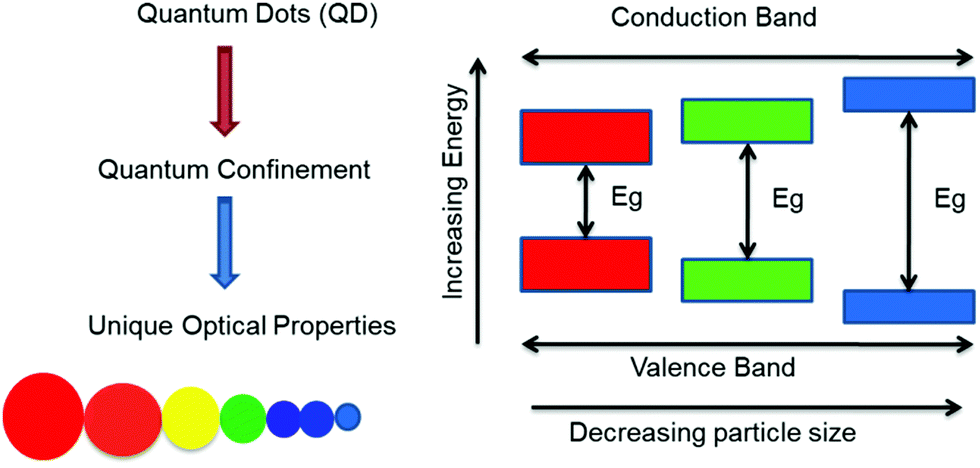 | ||
| Fig. 1 The schematic representation of quantum dots and their energy levels. | ||
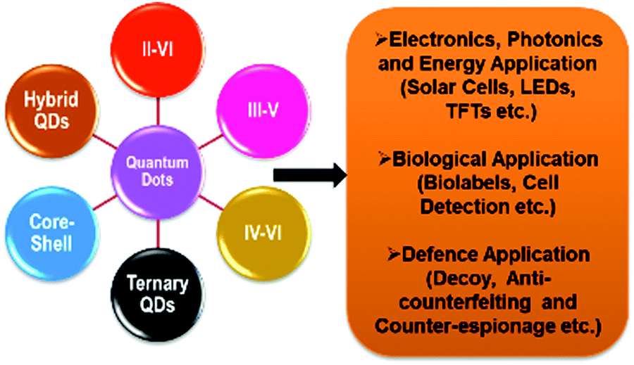 | ||
| Fig. 2 Major application domain of quantum dots. | ||
Numerous research groups have established a large variety of wet-chemical synthesis routes to obtain high-quality QDs in the size range of 2–10 nm with homogeneous size distributions and spherical morphology, termed as regular QDs.34,35 A common challenge faced by researchers while synthesizing such high-quality QDs is to achieve defect-free states. Nevertheless, one must keep in mind that interstitial defects are desired to a certain extent, such that their optical properties are not adversely affected, and that photonic application gets impetus and range. Exploring different reagents and reaction conditions, researchers demonstrated control over the QD size and shape. With this comes a realization that, under certain ideal experimental conditions, selective mature QDs can be isolated. While perfecting synthesis approaches towards regular QDs, scientists discovered unique optical absorption bands in the ultraviolet region in the case of CdSe. This finding was initially puzzling but soon led to excitement in the world of nanotechnology. The newly discovered kind of QDs was later named magic-sized nanoclusters (MSNCs) and will be discussed comprehensively in the next sections.
1.2. Magic-sized nanoclusters
Generally, clusters cover the size range between the bulk material and individual atoms or molecules. Herein, the so-called magic number denotes the particular number of atoms coordinating the central atom giving rise to a stabilised, close-packed structure less than 2 nm in size. On the basis of the chemical composition, driven by either different or similar types of atoms, clusters can be heterogenous or homogenous. Typically, the formation of clusters is a stochastic process, leading to the development of particles with varied cluster sizes.36,37The cluster size differs from several atoms to hundreds of atoms, and the consequential ensemble of a cluster is characterized by a broader size distribution. Some reaction settings yield clusters of a specific size which have high stabilities and consequently are formed in much larger quantities as compared to clusters of other sizes. Such clusters are frequently denoted as “magic” clusters because the number of atoms they possess is not arbitrary, but nevertheless is precisely equivalent to a “magic” number. A typical example of magic-sized clusters is the family of fullerenes, which includes C60, C70 and C84.38,39 The cluster stability in terms of structure and thermodynamics is attributed to the seamless coordination between their intrinsic and surface energy.40 Nanoclusters of many materials have been documented in recent times.
Silver nanoclusters (Ag NCs) having sizes of less than 2 nm have gained recognition due to their various applications in several fields, such as sensing,41 labelling, catalysis,42 and as antibacterial agents.43,44 The fascinating properties of these clusters are related to the molecule-like properties they possess, which leads to the generation of fluorescence emission.45 In recent years, researchers have provided a comprehensive account of the dependence of the optical properties of magic silver nanoclusters on their morphology as well as their possible applicability in detecting metal ions, small molecules, and proteins, biological imaging and studying chirality.46,47 In spite of the low photostability, many authors reported very intense fluorescence signals for AgNCs compared to AuNCs.12,48 Indeed, a multitude of techniques have been developed yielding fluorescent Ag NCs through stabilization in organic templates,49 biomolecules50,51 and interfacial etching using sulphur-rich compounds,52,53 as well as photoreduction of silver ions54,55 and sonochemical approaches.47 Each technique presents its own challanges in the analysis of mono-dispersity, stability, and quantum yield. Recent reports suggest that the crystal lattice and nature of nanostructures can be advantageously studied by tuning the physicochemical properties. Magic-sized gold clusters have two conceivable sources of fluorescence, the metal core and the interactive sites of the metal and surface ligands. The metal core charge states as well as the ligands are seen to have an effect on the fluorescence of gold nanoclusters. Bigioni et al.56 detected photoluminescence in the NIR spectrum for 1.1 and 1.7 nm particles of gold clusters. Similarly, poly(amidoamine) embedded hydrophilic Au NCs (Au8) with high quantum yield (QY) have been reported by Lees et al.57 Rather than a structured continuum, Au magic-size clusters can be considered as a series of discrete electronic transitions with specific character.48 Such properties facilitate the distinction amongst diverse sizes of particles. Some stoichiometries are predominantly stable, and it becomes possible to segregate nanoclusters of different sizes.48,58,59 Electrochemical experiments demonstrated that these nanoparticles possess molecule-like electronic states and a non-zero bandgap.48 The robust quantum confinement effect is key to size-dependent fluorescence, colour tunability and surface tailoring.60–63 Given these favourable properties, the applicability of AuNCs ranges from their use in biosensing,64 biological labelling,65–67 and bioimaging48 to electronics41 and catalysis.42
Likewise, magic clusters of other materials have also been reported and especially those of semiconductor nanoparticles, which have generated tremendous interest due to their fluorescence properties. In this direction, there are reports about II–VI, III–V and other magic clusters e.g. ZnSe,36,68,69 CdTe,70–73 InP,74–76 CdS,77 CdSe,78,79 and PbSe.80 Using an H2Se amine complex as the selenium source, Zang et al.69 prepared multiple families of ZnSe MSNCs via a thermal method. Oleic acid capped CdS MSNCs are reported from cadmium oxide (CdO) and thiourea. Duke and group73 reported CdTe MSNCs by a hot injection method using CdO–HAD (hexadecylamine) and Te-TBP (tributylphosphine) as precursors. Soloviev et al.81 stated that the huge surface to volume ratio governs the emission in CdSe MSNCs due to surface trapped states. Eichkorn and Ahlrich82 theoretically studied CdSe MSNCs and observed that the confinement effect on the energy levels of these tiny clusters is more enhanced than in larger particles. The focus of this review article is limited to CdSe magic clusters from group II–VI as it has been demonstrated that this material shows great potential for white light applications.
1.3. CdSe magic-sized nanoclusters
MSNCs of cadmium selenide (CdSe) are thermodynamically stable, semiconducting nano-crystals with sizes ranging from 1 to 2 nm that exhibit unique physical properties. Henglein and co-workers83 first observed MSNCs of II–VI metal selenides in the 1980s. The excellent stability of MSNCs in terms of structure and thermodynamics is attributed to the seamless coordination between their intrinsic energy and surface energy. The discussion hereafter focuses on cadmium selenide nanoclusters. The magic stability of these clusters has been directly accredited to the geometric structures and the full electron shells.32,84 They possess the capability of conjugating with proteins, which makes them, for instance, excellent markers for biological systems with stable luminescence.It is recognized that CdSe MSNCs are likely accumulated in specific numbers of CdSe pairs as well as unique structures so as to attain maximum binding energy with magic stability due to geodesic and electronic bonding factors.85 CdSe MSNCs are classified in families according to the specific number of atoms they have and the characteristic absorption peak, e.g., the (CdSe)13 and (CdSe)19 families, etc. Despite significant advances since their first discovery, with respect to synthesis, there is still a need for better understanding of the nucleation and growth dynamics as well as the resulting nano-cluster structure.66 Peng et al.86 were among the earliest researchers to focus on the slow reaction kinetics to synthesize these magic clusters.
The formation of magic-sized CdSe is known to be affected by several synthesis parameters, including the choice of capping agent, Cd-to-Se ratio, and reaction time.85 For stable MSNCs, the surface Cd and Se atoms are all three-coordinated atoms. In terms of size and composition, magic-sized nanoclusters exhibit similar properties to ultra-small nano-crystals. However, two fundamental properties can be considered as responsible to provide a distinction between MSNCs and ultra-small nano-crystals, viz, the type of growth mechanism and the absorption peak width. CdSe MSNCs display heterogeneous growth and have absorption bands of narrow FWHM (Full Width Half Maximum).87 For instance, by employing tetradecylphosphonic acid (TDPA) with cadmium oxide as the cadmium source, narrower peaks were repetitively seen at 285 and 349 nm, respectively, by the researchers. The peak stability during the preliminary growth stages along with the extremely narrow peak width was associated with thermodynamically stable clusters having a precise number of atoms.86
Concerning the size distribution, in recent years, a tremendous amount of work has unfolded exciting features. Magic-sized II–VI semiconductor nanoclusters show narrow peaks for absorption, the reason being that they exhibit a mono-size particle distribution, and thus have no contribution to the width of the absorption peak.87 Apart from this, narrower photoluminescence peaks have also been observed. For instance, Yu et al.88 reported a photoluminescence band with a FWHM as narrow as only 10 nm and an absorption FWHM of 8 nm, demonstrating unique optical behaviour. One of us has previously demonstrated the synthesis of MSNCs exhibiting a photoluminescence peak with a FWHM of 30 nm.89 In an effort to further tune the optical properties of CdSe MSNCs, the authors adopted a novel chemical approach using an organoselenium source, which avoided the use of toxic phosphines and amines.90 Some researchers73,85,91,92 reported that, during the formation of MSNCs, growth was observed where initially formed nano-crystals underwent a transition from a discrete size to a larger size (Fig. 3a). Other authors found that etching with butylamine can convert regular nano-crystals into nanoclusters (Fig. 3b).3 Another fascinating case by Yu et al.93 reported two absorption peaks arising at the same time, meaning that different families of nano-crystals start growing simultaneously. These nano-crystals were named as their own class known as magic-sized nuclei. The study demonstrated the concept of selective control of the synthesis process between magic-sized nanoclusters and regular QDs employing a thermodynamically driven strategy.
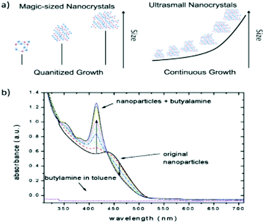 | ||
| Fig. 3 (a) The general growth mechanism for MSNCs vs ultrasmall nanocrystals. Reprinted with permission from ref. 87 [S.M. Harrell, J.R. McBride and S.J. Rosenthal, Chem. Mater., 2013, 25, 1199–1210]. (b) CdSe nanocrystals etched to magic-size employing butylamine, ref. 3 [C. Landes, M. Braun, C. Burda and M.A. El-Sayed, Nano Lett., 2001, 1, 667–670]. | ||
To understand and control the growth of semiconductor MSNCs, the precursors and reaction parameters are imperative factors in order to develop materials with well-defined optical and physical properties. One complication in growing CdSe MSNCs is to achieve a specific or exclusive family of mono-disperse nature. The fast development in synthesis procedures over the past years has facilitated the growth of CdSe MSNCs with various sizes. For example, Ping et al.94 focused on 2, 6, and 13 Cd atom clusters, i.e., Cd2Se2, Cd13Se13 and Cd6Se6 structures, exploring the structural aspect of CdSe MSNCs. Cd6Se6 has a wurtzite (cubic) structure of one unit cell with all atoms on the surface; thus, it is considered an extreme case. Cd13Se13, on the other hand, has a cage conformation with three fused unit cells with a larger wurtzite structure where each unit cell shares two faces with two other unit cells. Recently, it has been observed that stable Cd13Se13 clusters exist in a cage conformation with 10 six-membered and 3 four-membered rings, having 13 Cd and 12 Se ions with one Se ion in the ring center.94
With respect to the architecture of CdSe, Se atoms tend to arrange at the outer region of the MSNC, while the Cd atoms are rather found inside the MSNC. This arrangement takes place during the electron–hole relaxation process and is primarily manipulated by self-reorganization of the cluster surface, reducing the degree of unsaturation of the surface atoms. Cluster relaxation and re-organization of the surface are the major causes of structure distortion in comparison to the ideal wurtzite unit cell seen in the bulk. Cd dangling bonds get reordered, resulting in three coordination bonds with merely one dangling bond left.94 Ben et al.95 worked on the structural aspects of MSNCs, where special attention was paid to the (CdSe)x families (x = 13, 19, 33 and 66). It was found that the ligands played a key role while stabilizing the structure in the bulk, wherein the geometry was relaxed both in a vacuum and in the presence of a surfactant.
Among the interesting optical properties of CdSe MSNCs, the discrete electron–hole recombination occurring at the MSNCs’ surface and core contributes to their broad emission profile. The quasi-metallic behaviour of the initial wurtzite geometry is the critical factor when performing optimisations due to the existence of two Cd atoms coordinated at the surface of smaller clusters (n = 13, 19). This aspect results in smearing of the electrons at the edges and is attributed to the non-saturated valencies of the Cd atoms. Yet, upon saturation of the dangling bonds, a typical HOMO–LUMO gap is seen. It was reported that the fully coordinated atoms look a lot like the ideal tetrahedral disposition of the wurtzite structure as Cd atoms are brought in the plane fashioned by triply co-ordinated Se atoms.96,97 As a result, their geometrical surroundings are closer to planar trigonal coordination. Selenium keeps puckering outwards and thus forms a pyramidal coordination structure, resulting in an approximately 120° bond angle for Cd atoms at the surface, while that for Se atoms is around 90°.98 Deglmann et al.99 evaluated the structure of smaller semiconductor clusters and reported that, in the case of dimers such as (CdSe)2 and other units having only a few formula units (up to the heptamer), surface relaxation occurs quite independently from core relaxation.
Consequently, it is essential to permit relaxation in the structure with the employment of carboxylate ligands to suitably design model clusters. Ben et al.95 employed density functional theory (DFT) to gain thorough knowledge regarding optical absorption, particularly the nature of the exciton peak, and the structure of CdSe nanoclusters. It was found that with ligands, the density of states associated with clusters having ideal wurtzite structure displayed a clear HOMO–LUMO gap. This gap became wide after saturation of the dangling bonds with the ligands.
Ouyang et al.88 pursued their interest in assessing the size of MSNCs by emission and absorption spectroscopy. They found that the band edge non-resonance photoluminescence (NPL) of the analysed MSNCs had a narrow bandwidth (FWHM), typically seen in a single dot rather than ensemble emission spectra. The magic-size family with its first absorption peak at ∼463 nm emitting at 465 nm corresponded to a diameter of ∼2.05 nm, which was calculated employing the formula for computation given by Yu et al.100 For estimation of the size distribution in terms of the number of atoms, it was assumed that the volume of a MSNC is proportional to its number of atoms.101 Various stable structures of CdSe MSNCs having a different number of atoms in their cubic crystal structure in the gas phase analysed using the PBE0 functional are depicted in Fig. 4.102 Generally, the presence of discrete and sharp absorption peaks are observed at a fixed position with broad emission. However, this trend has been recently seen where only sharp emission was witnessed mainly due to their discrete sizes.85
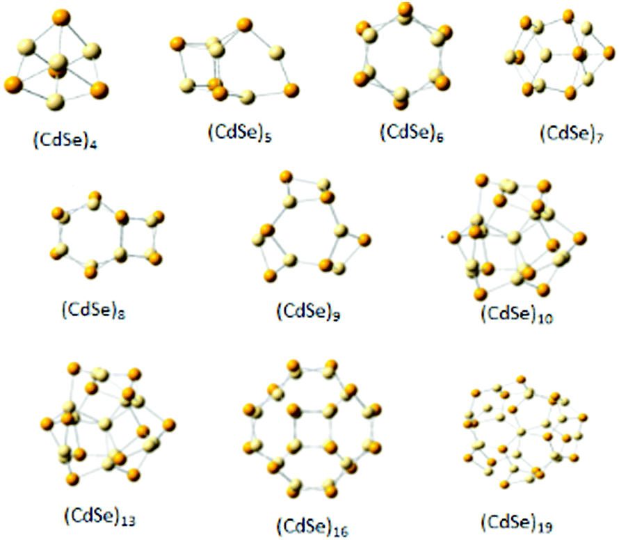 | ||
| Fig. 4 Different structures of CdSe clusters with defined numbers of Cd and Se atoms. Reproduced from ref. 102 [Y. Cui, Z. Lou, X. Wang, S. Yu and M. Yang, Phys. Chem. Chem. Phys., 2015, 17, 9222–9230] with permission from the PCCP Owner Societies. | ||
Zhu et al.83 reported clusters having sharp HOMO–LUMO absorption peaks. Apart from the bandgap absorption peaks at 414 to 422 nm, two additional absorption peaks lying between 382 and 398 nm and 352 and 365 nm were frequently observed. This variation can be attributed to the experimental conditions. The absorbance of the two peaks having shorter wavelengths is weaker because of the secondary and tertiary electronic transitions of MSNC-415.
Recently, Bootharaju et al.103 have also published a review article on II–VI nanoclusters. The challenges faced during synthesis and techniques used for characterization of such MSNCs were very well highlighted. However, this review focuses mainly on CdSe nanoclusters, and their potential in white light devices is explored. Having published several articles ourselves in this area,40,78,89,90,104–106 and through the literature, it has been realized that there are tremendous challenges in the synthesis and tailoring of CdSe MSNCs. Further, it has been noticed that the literature is very scattered, which prompted us to summarize the recent advances in their research and discuss future perspectives. This article provides a comprehensive review of the past research carried out concerning CdSe MSNCs. The challenges faced during various reported synthesis methods are addressed.
2. Synthesis of CdSe MSNCs
2.1. General background on chemical synthesis
Given the great potential for application of MSNCs in a whole gamut of technological fields, there is a constant need for the development of reliable synthesis routes towards MSNCs of controlled size and, hence, properties. The noteworthiness of the synthesis methods came into realisation with the reaction rate achieved by Murray et al.,102 which is extremely fast for direct isolation of small nano-crystals. Several techniques have been established for synthesizing CdSe MSNCs, which are typically based on the decomposition of suitable Cd and Se containing precursors.3,32,36,40,73,85,88,107–111 Cadmium chloride, CdCl2, is the most conventional Cd source, while CdO is a commonly applied alternative for the synthesis of CdSe clusters and other semiconductors. Concerning Se, there is no consensus about the most suitable source, and various Se-based compounds have been applied successfully.Among the many synthesis methods yielding CdSe nano-crystals of different sizes, the thermal decomposition method is the decomposition of organometallic compounds containing chalcogenides and metals that are employed as precursors in high-boiling organic solvents at relatively high temperatures (∼300 °C). This approach leads to CdSe MSNCs of good crystallinity and narrow size distributions. To achieve this, the crucial aspect is a rapid nucleation step at the initial stage of the reaction, followed by nucleus growth, while suppressing any further nucleation. In this vein, three approaches are typically followed: the single-source precursor approach and hot injection-based synthesis,112,113 as well as the solution-liquid-solution mechanism. In the hot injection method, a huge amount of monomer is produced in a short time span by prompting a burst of nucleation upon quick addition of the precursor mixture. In other words, highly reactive precursors are rapidly mixed at an elevated temperature.114 Herein, MSNC growth is commonly controlled by one of the two following strategies: adjusting the surface energy of a particular facet of the nano-cluster by providing a suitable surface-stabilizing ligand or controlling the concentration of reactants. Although there are some problems associated with thermal decomposition methods, such as the need for air-free reaction conditions, the use of toxic reactants, and limited availability of single-source precursors, it constitutes a very common method.115,116 Solvothermal and hydrothermal methods are alternative processes employed for the synthesis of nanoclusters. The solvothermal approach uses organic solvents as reaction media, while the hydrothermal route consists of a special case using water as the solvent. Irrespective of the solvent, the reaction is carried out in a closed vessel, i.e., autoclave, facilitating a pressure increase upon heating to a specific temperature, thereby increasing the precursor solubility. However, crystallization of CdSe MSNCs of controlled shape remains a big challenge when using the solvothermal approach. The Wulff facet argument is certainly the most stated and featured characteristic model for controlling the MSNC shape, suggesting that the shape is governed by the surface energy associated with each face or each facet of the crystal.117 Many researchers explored the fabrication of MSNCs by altering reaction settings like the temperature, capping ligands, and reaction media, or by employing different Cd and Se sources. Yet, many of the applied methods still suffer from the formation of multiple families of MSNCs,85 while there are very few studies that report the successful synthesis of a single MSNC family.40 Moreover, the synthesis of single-family MSNCs via conventional hot-injection approaches has been acknowledged to be quite challenging.118,119
2.2. Aqueous synthesis route
Over the past years, organometallic approaches, along with many other synthesis routes, have evolved for the controlled synthesis of high-purity CdSe nanoclusters, boasting monodisperse size and morphology. A prevailing problem of the organometallic approach consists of the high-temperature annealing of the particles within a few seconds of the process, which hinders particle growth and creates a disordered synthesis environment. The fabrication schemes considered to date produce large-sized NCs followed by sequential etching through chemical agents, resulting in desirable MSNCs.3,87 Moreover, some have reported the use of thiols as capping agents to process semiconductor NCs.13–15 This alternative approach has two prominent advantages over the organometallic technique, namely increased binding affinity between the thiol ligand and the NC surface compared to that of trioctylphosphineoxide (TOPO) and immediate nucleation at low temperature with steady crystal growth as the temperature rises. Water-based synthesis has several interesting features like accessibility, bio-friendliness, multiplicity and low-temperature activity that make this process superior to others mentioned earlier. For instance, due to their cellular compatibility and water solubility, bio thiols like glutathione (GSH) and cysteine (CYS) can be employed as stabilizers for the synthesis of semiconductor NCs that discretely belong to the II–VI group like CdSe. For example, Xia et al.79 synthesised highly stable, water-dispersible CdSe MSNCs employing homocysteine (HCY) as a capping ligand. The MSNC size was tunable in the range of 1.2 to 2.0 nm based on the reflux time. The so formed nanoclusters exhibited a photoluminescence quantum yield of 1.4%, which was nearly equivalent to that of CdSe MSNCs prepared by an organometallic route. The general representation of the synthesis path is shown in Fig. 5. Aiming to assess the suitability of CdSe MSNCs as optical bio-labels, Silva et al.109 reported the synthesis of 1.6 nm sized CdSe MSNCs in an aqueous solution using cadmium perchlorate hexahydrate as a cadmium source and NaHSe as a selenium source with 1-thioglycerol as a biocompatible capping ligand, further reporting their characterization by optical microscopy techniques. The obtained CdSe MSNCs exhibited a wurtzite structure, along with characteristic deep level defects. They further exhibited thermodynamic stability and bright luminescence in a biological microenvironment, covering a broad spectral range. Because of the higher photostability, these MSNCs were employed in a biological context, which included the construction of novel fluorescent probes facilitating the imaging of living cells as well as the study of membrane-bound receptor transportation. This represents a fascinating case for the application of CdSe MSNCs in intracellular studies.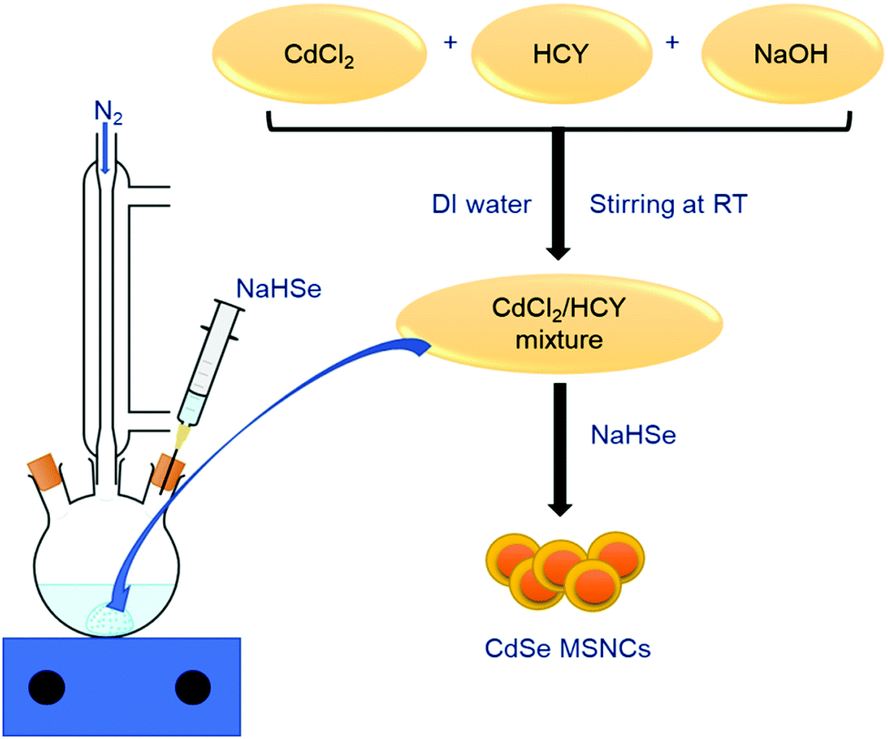 | ||
| Fig. 5 Representation of CdSe synthesis via an aqueous route.79 | ||
2.3. Non-aqueous synthesis route
A straightforward and highly reproducible method towards two stable magic-sized CdSe families was proposed by Liu et al.,30 using N-oleoylmorpholine as the reaction medium in a one-pot approach conducted at different growth temperatures. The resultant pure 392 family was attained by passivating the surface with long chain fatty acids and keeping the temperature around 100 °C, while the 461 family was also seen at higher temperature i.e., around 150 °C. They emitted white light with a QY of more than 25%. These nanoclusters maintained their white light emitting properties at least for two months without compromising the quantum yield. Fig. 6 presents the schematic of their synthesis, the XRD pattern and the corresponding UV-vis and photoluminescence (PL) spectra when passivated with lauric and stearic acid.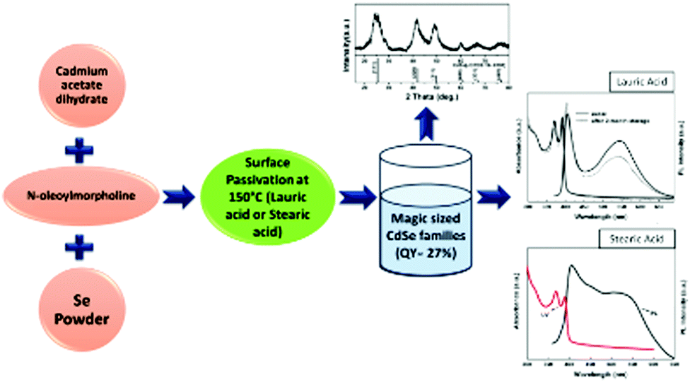 | ||
| Fig. 6 Schematic representation of the synthesis procedure using N-oleoyl morpholine as the reaction medium in a one-pot approach with XRD, UV and PL diagrams. Redrawn and reproduced from ref. 30 [X. Liu, Y. Jiang, C. Wang, S. Li, X. Lan, and Y. Chen, Phys. Status Solidi., 2010, 207, 2472–2477]. Copyright Wiley. | ||
Kasuya et al.32 found an alternative, inimitable way of producing stable CdSe MSNCs: following a reverse micelle method, the addition of cadmium nitrilotriacetate with sodium selenosulphide, decylamine and toluene resulted in micelles moving up in the layer of toluene, ultimately yielding MSNCs. Interestingly, Lawrence et al.120 firstly reported a colloidal method for the synthesis of white-light emitting, ultra-small nanoclusters (∼1.5 nm). Such nearly pure white-emitting nanoclusters were attained with selective manipulation of the surface chemistry (surface trap-states along with passivating ligands) and by controlling the substitution of halide ions. The chemical aspects of the surface passivating ligands surrounding the nanoclusters are of tremendous importance. In order to investigate their properties in varied settings, it is imperative to disperse the capped nanoclusters in a wider variety of polar and non-polar solvents. Therefore, the authors established a direct fabrication and purification approach for ultra-small CdSe passivated by poly(ethylene glycol) thiolate with a diameter of less than 2.0 nm having such solubility features.120
For capping agents, not only their chemical nature but also their purity plays a key role in CdSe MSNC growth, as demonstrated by Newton et al.121 The authors presented a low-temperature (∼70 °C) approach for the synthesis of trioctylphosphine oxide (TOPO)-capped magic-sized CdSe nanoclusters exhibiting green light emission. The experiment involved the reaction of TOPO–cadmium acetate precursors with trioctylphosphineselenide. Varied purities of TOPO were tested for nano-cluster formation as to its effects and how it influences the development procedure. The fabrication approach was also stretched for preparing magic-sized CdSe nanoclusters stabilized by trioctylamine (TOA), lauric acid (LA), oleylamine and ethylphosphonic acid (EPA). More prominently, the investigation revealed that the nature of the Cd precursor plays a crucial role in the nano-cluster growth mechanism. The synthesis of TOPO, EPA, LA, and TOA-stabilized CdSe NCs exhibited slow and continuous growth of ultra-small MSNCs, while OA-capped NCs displayed quantized growth of different families.
Pertaining to the ligands used in synthesis, CdSe MSNCs exhibited either broad luminescence or broad luminescence along with band edge emission. Molecular clusters of chalcogenides were firstly developed by Dance et al.,111 and it was found that selenophenol and sulfophenol can also be used for the preparation of CdSe nanoclusters. It was claimed that, by using these ligands, the clusters do not degrade or aggregate into larger particles.111,112 Studies related to shape regulation of colloidal nanoclusters might further deliver some insights to understand this significant phenomenon in general. Clusters consisting of 4, 8, 10, 17 and 32 atoms were synthesised by varying the Se source and solvent instead of arresting or controlling the growth of nano-crystals. Analysis of the electronic and optical properties of the obtained structures unveiled a dependence of the bandgap on the size in the range of 1/r to 1/r2, where r is the radius of the cluster.81,122Table 1123 provides an overview of ligands used for MSNCs in accordance with their respective bandgap wavelength.
| Ligands | Maximum absorption peak (nm) | Ref. |
|---|---|---|
| Docosanoic acid | 463 | 123 |
| Acetic acid | 463, 413, 363, 389 | 85,124 |
| TOP and TOPO | 408 | 93 |
| Oleic acid | 410, 364, 391, 395, 372 | 89,123 |
| 1-Napthoate | 412 | 92 |
| Stearic acid | 414 | 66 |
| TOPO | 414 | 107 |
| Benzoate | 418 | 85 |
| TDPA | 349 | 86 |
| ODPA | 350 | 32 |
| Decylamine | 380, 415 | 32 |
| Lauric acid | 395, 373 | 85 |
| Diisooctylphosphinic acid | 383, 414 | 73 |
It can be easily interpreted by analysing the ligands used for the synthesis of MSNCs that two different categories of magic clusters exist. The first category comprises those clusters that are formed with the aid of phosphonic or phosphinic ligands, while the MSNCs obtained using other fatty acids as ligands are grouped in the second category. This characteristic or trend could have two explanations. The first is that the exact size of the MSNC or, in other words, the exact number of Se and Cd atoms, depends on the ligand choice. The second explanation could be the bandgap energy being dependent on the ligand, despite the same size nanocluster being formed. Various studies published in recent years support the latter argument. For instance, Landes et al.3 observed such a ligand-dependent bandgap when replacing TOPO ligands with butylamine ones. Moreover, a significant change in absorption, i.e., a blue shift, was ascribed to the etching of the MSNCs by shorter chain primary amines.
Yu et al.125 observed that the addition of 3% TOP boosted the yield of fatty acid capped CdSe MSNCs. However, an increase in TOP to 13–50% induced homogenous growth of a new family of MSNCs. Interestingly, yet another family of MSNCs emerged upon a further increase of the TOP concentration to 65%, having bandgap absorptions at 408 and 463 nm. A continuous increase of the percentage of TOP yielded a fourth family at 408 and 356 nm having TOPO/TOP bound to Cd atoms at the surface, while the initial 433 and 463 nm MSNC families started to disappear. The authors proposed that the size of the MSNCs was affected by the degree of super-saturation of the monomer precursor, which ultimately determines whether MSNCs will form or not. Herein, super-saturation was linked to the CdSe monomer concentration as well as the presence of the fatty acid and acetic acid ligand. Moreover, the higher the concentration, the higher the degree of super-saturation, which in turn fostered the formation of MSNCs. Xie et al.108 obtained similar insights regarding this aspect of the formation of nano-crystals, describing a reaction that was driven by chemical instead of nucleation kinetics, once reaching a critical degree of super-saturation. Super-saturation of the reaction solution was based on the concentration and solubility of the monomer precursor.
Interestingly, other work found that, for the successful synthesis of MSNCs, the presence of an amine was required, while phosphinic acid alone was deemed non-suitable.73 This observation was attributed to the decrease or increase of the activation barrier, which in turn may affect the coordinating solvents and hence the formation of MSNCs. It is likely that a weaker binding ligand, such as an amine, decreases the activation barrier of MSNCs as the phosphinic acid binds more efficiently to Cd as compared to amines.97 Xie et al.108 and Yu et al.125 observed a lower synthetic yield of MSNCs when fatty acid ligands were added in addition to an amine. Interestingly, this finding is contradicting the aforementioned study by Yu et al.93 who observed that the existence of a small amount of TOP acting as a coordinating solvent during the synthesis, along with the use of fatty acids acting as ligands, provided a higher MSNC yield. This is likely due to stronger binding of fatty acids in comparison to TOP on the surface of the nanoclusters. Also, amines bind more strongly than fatty acids.97
A non-injection, one-pot approach was reported by Ouyang et al.85 where three families of CdSe MSNCs referred to as 395, 463 and 513 were synthesised employing Cd(OAc)2·2H2O and selenium as Cd and Se sources, respectively. The absorption and photoluminescence spectra of the so-prepared MSNC families are depicted in Fig. 7. The authors explored the effect of 1-octadecene (ODE) and fatty acids on the growth of MSNCs under a controlled nitrogen atmosphere and in a temperature range of 120 to 240 °C. Reliant on the synthetic conditions of a high Cd to Se ratio of 4![[thin space (1/6-em)]](https://www.rsc.org/images/entities/char_2009.gif) :1 and low myristic acid to Cd feed molar ratio of 2.7, MSNC growth was observed.
:1 and low myristic acid to Cd feed molar ratio of 2.7, MSNC growth was observed.
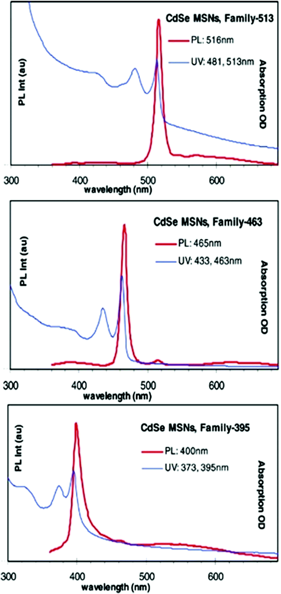 | ||
| Fig. 7 Absorption and photoemission spectra of three families of CdSe MSNCs, namely 513, 463 and 395. Reproduced with permission from ref. 85 [J. Ouyang, M. B. Zaman, F. J. Yan, D. Johnston, G. Li, X. Wu, D. Leek, C. I. Ratcliffe, J. A. Ripmeester and K. Yu, J. Phys. Chem. C, 2008, 112, 13805–13811]. Copyright American Chemical Society. | ||
CdSe NCs were prepared by Sun et al.126 in 1-octadecene, a non-coordinating solvent, with paraffin liquid in the presence of a sole ligand long-chain primary alkylamine. Herein, ODE-selenium and a salt of Cd with a fatty acid were employed as precursors. The so formed nanoclusters met three essential parameters for higher quality nanoclusters, a narrow distribution size with broad range size tunability and a moderate photoluminescence quantum yield. Additionally, it was seen that nanoclusters could be fashioned with predictability in size by the regulation of the relative molar ratios for the alkylamine-Cd precursor. The narrow size distribution of regular-sized “nuclei” (FWHM of 23 nm), and any subsequent narrowing growth procedure vanished due to quenching. This indicated changed and dissimilar growth as well as nucleation kinetics in place of the previously established focusing and defocusing theory, which in principle comprises narrowing and broadening of a particle size distribution. By analysing the conversion factor for the precursors along with the concentration for magic-size clusters as well as regular size nuclei, a refined and elusive mechanism of secondary nucleation and quantized fusion was projected. According to this mechanism, MSNCs are initially formed as critical nuclei, followed by coupling of these quantized critical nuclei and subsequent fusion of regular-sized nuclei with stoichiometric monomers. The quantized fusion transformation may well be controlled by the nature as well as the ratios of the activating agent and the nucleating agent. Another point to be noted here is that such transformations are extremely swift; hence, they ought to be regulated kinetically. The classical ester aminolysis reaction might be the basis of the molecular mechanism of monomer formation.126
2.4. Organometallic route
Assessing the suitability of various Se precursors, Jadhav et al.40 used a series of 1,2,3-selenadiazoles as Se precursors for the first time to synthesize CdSe MSNCs. This precursor class can be promptly prepared by manually grinding the reactants through a solvent-free method. Hence, the reactivity of 1,2,3-selenadiazoles towards cadmium salts to synthesize CdSe MSNCs and how different Se precursors affect the MSNC formation were observed and discussed. Synthesis of MSNCs was performed using oleic acid as the passivating agent in diphenyl ether (DPE) as the solvent and an N2 environment under reflux conditions (150 °C)40 or under microwave irradiation104 in order to shorten the reaction time and to study the variation in the source of thermal energy. This reaction procedure is presented in Fig. 8 (top). Khanna et al.105 synthesized magic-sized CdSe nanoclusters through a green synthesis approach, using edible oils such as castor oil, olive oil, mustard oil, cod liver oil and coconut oil as capping agents as presented in Fig. 8 (bottom).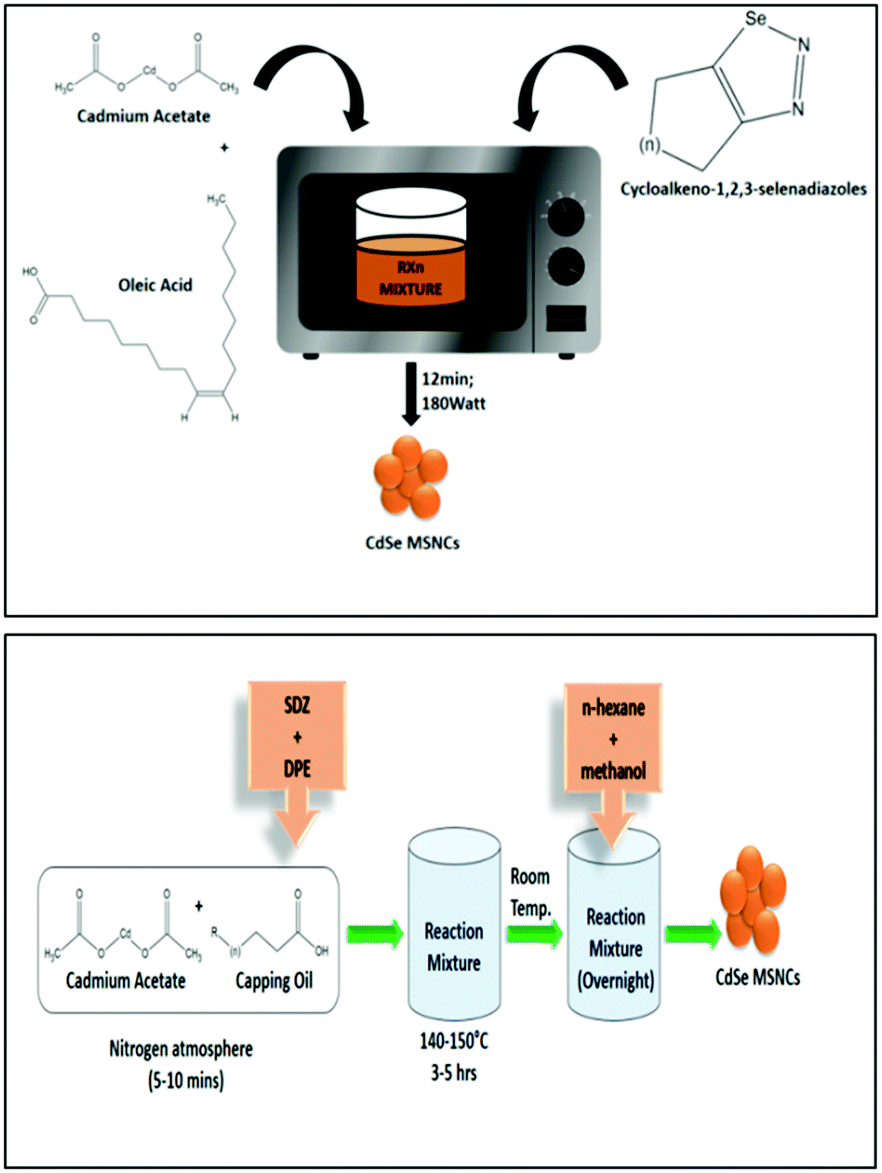 | ||
| Fig. 8 A systematic representation of the microwave synthesis of CdSe MSNCs, ref. 104 (top). Green synthesis approach towards CdSe MSNCs, ref. 105 (bottom). | ||
It is a typical perception regarding the synthesis of MSNCs that, after their formation, they hold their measure in terms of size and do not grow any further at elevated reaction temperatures or more extended time. Among the aliphatic and aromatic classes of 1,2,3-selenadiazoles, it was seen that acyclic aliphatic 1,2,3-selenadiazoles prompted the development of a sole family of MSNCs while regular-sized quantum dots (RSQDs) alongside MSNCs were formed by aromatic ring-substituted selenadiazoles and in particular most prominently provided effective experimental approaches and tactics for single-sized nanoparticles desirable in varied applications.40
There are a few organometallic reagents that suit tailoring of the optical properties and shapes and sizes of semiconductor nanoparticles, especially those of II–VI and III–V QDs, including MSNCs. However, these organometallic precursors are air-sensitive as well as pyrophoric in nature, thus offering limited scope for the synthesis of such high-tech materials at reasonably lower temperature. The synthesis methods using such organometallic reagents require much higher temperature to ensure good crystallinity and greater thermal stability of the nano-crystals. Most organometallic precursor-based approaches involve TOP and TOPO reagents in combination with separate reactants or molecular precursors similar to common routes towards QDs. Despite the challenges related to the organometallic route, successful examples are published in the literature. For instance, the single-source precursor approach was used by Soloviev et al.81 to synthesize a cluster of CdSe that contained up to 32 Cd atoms, using phosphine as a capping agent. Alternatively, the reaction temperature was lowered from 360 °C to about 130 °C in the Murray method by Landes et al.,3 allowing one to slow down the reaction kinetics post drying the TOPO. The reaction temperature was again raised slowly for growth from 130 °C to 140 °C for precursor injection, thereby producing nanoclusters having diameters as small as 1.6 nm.
The various synthesis methods and the properties of the so-formed MSNCs along with their growth mechanism are summarised in Table 2.
| Method | Precursors | Growth conditions | Size domain and mechanism | Ref. |
|---|---|---|---|---|
| Aqueous | CdCl2·2.5H2O, HCY, NaHSe | Heat (Δ) at 100 °C for several hours | 1.2 to 1.9 nm depending upon the reaction time, in situ nucleation and growth | 79 |
| Cd(ClO4)2·6H2O, thioglycerol, NaHSe | 60 °C in an inert atmosphere | 1.6 nm, in situ nucleation and growth | 109 | |
| CdSO4·8/3H2O, poly-ethylene glycol Na2SeSO3 | Δ at 30 °C for 30 min | 1.6 nm, in situ nucleation and growth | 120 | |
| Non-aqueous | Cd(OAc)2·2H2O, N-oleoylmorpholine, Se | Δ at 100–150 °C | 1.7–2 nm, in situ nucleation and growth | 30 |
| Cadmium nitrilotriacetate, micelles, decylamine, Na2SeSO3 | Δ at 45 °C | 1.5 nm, in situ nucleation and growth | 32 | |
| Cd(OAc)2·2H2O, Se, TOP, TOPO | Δ at 70 °C for 36 h | 1.8 nm, in situ nucleation and growth | 121 | |
| Organometallic | Cd(OAc)2·2H2O, OA, 1,2,3-selenadiazole | Δ at 150 °C for 3–5 h | 1.2 to 1.5 nm depending upon type of selenadiazole, in situ formation of MSNCs via extrusion of Se from precursor | 40 |
| CdCl2, Se(SiMe3)2 | Stirred at room temperature overnight | 1.7 nm, typical organometallic method and in situ formation | 81 |
3. Characterization of CdSe MSNCs
A major challenge when analytically assessing tiny clusters, such as CdSe MSNCs, is the absence of straightforward means and methods to characterize them. The determination and understanding of size by transmission electron microscopy (TEM) is often considered as accurate. Nevertheless, it should be kept in mind that preparation of a TEM sample, which typically originates from a colloidal form, may also affect the final result and, hence, challenge the understanding of the morphology, size, and size distribution. X-ray scattering is an alternative method to determine the particle size, yet it provides ensemble-averaged results.91 Small angle X-ray diffraction (XRD) analysis is another useful option to assess size and aggregation, while X-ray photoelectron spectroscopy (XPS) is useful when seeking insight into surface properties. Optical spectroscopy is one of the most versatile characterization techniques and the simplest way to understand the absorption and emission behaviour of MSNCs. Particularly, UV-visible absorption spectroscopy (UV-vis spectroscopy) is undoubtedly the most frequently used analytical method for the estimation of the size of MSNCs.A comprehensive approach based on sizing curves from larger nano-crystals on the basis of X-ray diffraction data and transmission electron microscopy together with UV-vis absorption is the most effective and popular way of estimating the size of a nano-cluster smaller than 2 nm.
The optical properties of CdSe MSNCs are strongly governed by the density of states, which is significantly affected by the nano-crystals’ surface structure. For instance, dangling bonds at the surface of the nanoclusters may cause luminescence quenching as a result of non-radiative recombination.127 The surface of CdSe nano-crystals comprises 70% Cd atoms and 30% Se atoms, approximately, out of which the Cd atoms are mostly ligand passivated, and the bare Se atoms produce dangling bonds leading to mid-gap states.128
In most cases, the surface chemistry of the nano-cluster results from the competition between the electron-to-vibrational energy transfer and Auger relaxation in the hot carrier's intra-band cooling, as well as between radiative recombination and hole or electron-trapping processes in the band-edge excitons. Steady-state and time-resolved photoluminescence (PL) spectroscopy and transient absorption (TA) spectroscopy serve as excellent tools to monitor the surface chemistry effects on the exciton relaxation process. With time, the TA spectrum evolves, revealing the band-edge's relaxation dynamics or hot excitonic states (electronically). The obtained spectra can also be applied to recognize the ligand's role in the decay process of the excitonic electron or hole. Typically, the decay dynamics are multi-exponential as the hole and the electron both have separate decay channel sets. PL and TA spectroscopy collectively provide the rate constants and suggest the mechanisms for the decay processes. In nano-crystals, the hot carriers’ intra-band relaxation takes place through different mechanisms, such as Auger recombination, transfer of energy to vibrations of surface ligands, and phonon-assisted relaxation. These intra-band relaxation processes are non-radiative, producing heat as a by-product, and thus offer easy monitoring by the dynamics of photo-induced absorption. As the inter-band relaxation has both non-radiative and radiative recombination pathways, the yield and rate of PL become a potent and convenient substitute or complement to TA for examining the relaxation from the band edge. According to Peterson et al.,129 quenching of PL in nano-crystals takes place when the non-radiative recombination of the excitons, i.e., the trapping of holes or electrons to a localized orbital (energetically accessible) in the lattice of a nano-crystal or on its surface, is faster than the radiative pathway, which may occur in microseconds (Pb-chalcogenide QDs) or tens of nanoseconds (Cd-chalcogenide).
A sufficient upsurge by the ligand in the competitiveness of radiative recombination (for the PL yield and exciton decay) has been observed upon removal of the thermodynamic trap via surface passivation by suitable ligands. Usually, for the passivation of electron traps on the surface, under-coordinated metal cations are used, whereas σ-donating ligands are used in the case of CdSe QDs, which maximizes the average lifetime of the exciton and enhances the yield of PL.129 Xia and co-workers79 studied the PL decay at PL maxima in magic-sized CdSe nano-crystals. They focused upon four decay times in the range from 2.1 to 188.6 ns with a mean PL decay time of nearly 80 ns. Such a relatively long PL decay time is a valued property for luminescent probes, which can be used for further applicability.
One of us has previously reported89 single-family CdSe MSNCs. The obtained XRD pattern unveiled a cubic structure with five focal diffraction peaks at (111), (200), (220), (311) and (400) indicating a zinc blende crystalline phase. The authors also studied the surface properties and elemental composition by XPS. Further, FTIR analysis allowed for the better understanding of the adsorption mechanism of oleic acid ligands on the surface of the CdSe nano-cluster, unveiling chemisorption of oleic acid on the CdSe MSNC surface through the ligand's carboxy groups. In particular, the complementary data set obtained by XPS and FTIR analysis articulated that the bonding between the carboxy group and the metal was bidentate in nature (both of the oxygen atoms contributed equivalently). Subsequently, high resolution transmission electron microscopy (HRTEM) indicated the presence of lattice fringes and point defects. Concentric rings were present in the selected area electron diffraction (SAED) because of the specific crystal structure (zinc blende), which confirmed the material to be remarkably crystalline. Moreover, small angle XRD has been shown to be a useful tool for understanding the particle size and lattice spacing, which definitely is a piece of powerful information desired for such tiny clusters, more so in view of the limited tools available to date to understand their properties.
Edible oil mediated magic-sized CdSe nanoclusters through a green synthesis approach105 were characterized using XRD, IR, UV spectrophotometry and PL spectroscopy. UV-vis spectroscopy showed similar absorption profiles for CdSe MSNCs obtained using mustard oil and olive oil, and only the formation of magic-sized CdSe nanoclusters was seen in this reaction. Conversely, a mixture of QDs and MSNCs was observed in reactions using coconut oil and cod liver oil. QDs as the sole morphology were formed when castor oil was used in the reaction. The PL spectra of the magic-sized CdSe nano-crystals capped with olive oil and mustard oil showed broad emission, inferring their white light characteristics; however, no such broad emission was observed for the nano-crystals capped with castor oil and cod liver oil, the PL profiles of which were similar to those of non-magic crystals. The PL intensity of the sample capped with mustard oil demonstrated the brightest white-light emission amongst the others (Fig. 9b). The magic-sized nano-crystals obtained from the capping of mustard oil were shown to be stable for around a year as they maintain their optical properties. The FTIR spectrum was reported for all the samples to identify the presence and nature of the interactions between the nano-crystals and the capping ligands. All the samples had fatty acid capping; therefore, all spectra showed the presence of organic moieties and similar functionalities. The Raman spectrum was also recorded for all samples, showing similar patterns as the functionality of the used capping agents was alike. The XRD patterns confirmed the formation of zinc blende magic-sized nano-crystals with key reflections at (110), (220), and (311). HRTEM images of the sample capped with mustard oil show that the small particles are elongated, ranging between 1.5 and 2.0 nm, and the presence of lattice fringes was also marked. Diffuse rings for the sample capped with mustard oil were observed in the SAED pattern and the amorphous nature of the elongated particles was also observed.
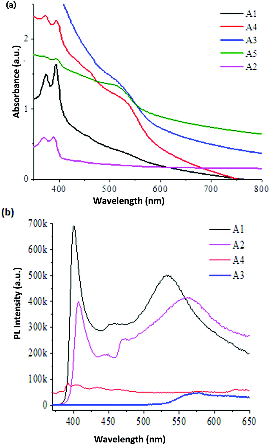 | ||
| Fig. 9 (a) UV-vis and (b) PL decay curve of CdSe MSNCs (A1–A5 are CdSe MSNC samples reported with different capping agents, e.g., olive oil, mustard oil, coconut oil, castor oil and cod liver oil (A1–A5). Reproduced with permission from ref. 105 [P. K. Khanna, A. Jadhav and P. V. More, J. Nanosci. Nanotechnol., 2020, 20, 2946–2954]. Copyright American Scientific Publishers. | ||
Jadhav et al.40 characterized their magic-sized CdSe nano-crystals using XRD, XPS, optical spectroscopy (UV-vis and PL), Raman spectroscopy, HRTEM, EDAX and TGA analysis. The formation of magic-sized CdSe nano-cluster families was observed by optical spectroscopy with absorption bands at 390 nm and 450 nm. The particle size was determined based on UV-vis spectroscopy and XRD analysis. The HRTEM image showed the aggregation of CdSe nanoclusters, but failed to tell more about the lattice structure and morphology (Fig. 10). EDAX analysis was also performed to know the proportion of Cd and Se elements. The surface defects of the clusters were studied by PL decay as for the broad emission peaks (560 nm) a long decay time was observed.
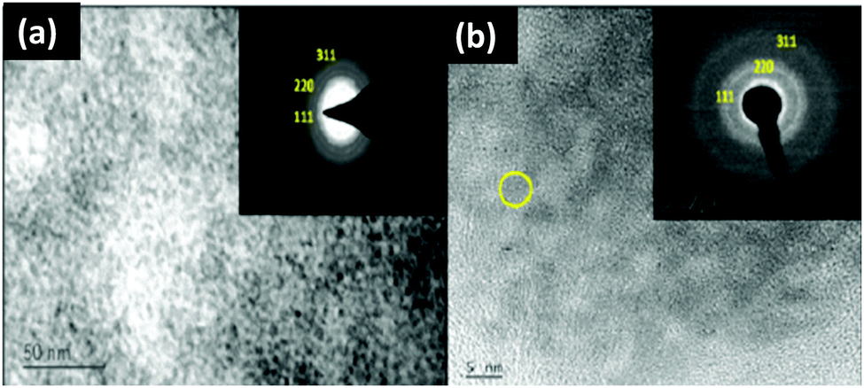 | ||
| Fig. 10 TEM images of CdSe MSNCs using (a) an acetophenone derivative of 1,2,3-selenadiazole (scale – 50 nm) and (b) aromatic 1,2,3-selenadiazole as the source of selenium (scale – 5 nm). Reproduced from ref. 40 [A. A. Jadhav and P. K. Khanna, New J. Chem., 2017, 41, 14713–14722]. Copyright Royal Society of Chemistry. | ||
Kudera et al.91 worked on a sequential growth approach towards magic-sized CdSe nano-crystals. They performed TEM analysis and reported that these nano-crystals have crudely spherical shapes without any aggregation. Furthermore, MALDI-TOF-MS was performed, yet no proper fingerprints of the original clusters were observed. Landes et al.3 used hyper Rayleigh scattering for the comparison of the effect of n-butylamine addition on the small (1.6 nm) and large (3.2 nm) CdSe nano-crystals. This scattering technique is an experimental method for the detection of the non-linear response of colloidal materials. In this study, the surface modification consisted of n-butylamine, which influenced the physical and electrical properties of the small nano-crystals. The second harmonic behaviour of the small nano-crystals showed deviation in the behaviour as compared to the large nano-crystals. Precisely, the second harmonic response versus nanoparticle concentration was reported as non-monotonic; however, upon addition of n-butylamine, monotonity was re-established.
Sun et al.126 obtained CdSe nano-crystals having multi-resolved and sharp electron transitions in their absorption and PL absorption profile. Mono-disperse nanocrystals with a larger area could be observed in TEM images. The morphology of the nano-crystals changed from cubic to hexagonal, which indicated the transition in structure from zinc blende to wurtzite. This phase transformation was further supported by XRD patterns. The comparison between the PL and absorption spectra clearly demonstrated the influence of the ligand composition on the phase transition.
Scanning transmission electron microscopy (STEM) is also an excellent tool to image nanostructures at the atomic level with good chemical sensitivity. Pennycook et al.130 have reported a very detailed STEM analysis of CdSe nanoclusters. Fig. 11(a) shows a STEM image of CdSe nanoclusters having a size about 3 nm. Foos et al.131 also reported the synthesis of CdSe QDs in different solvent mixtures. These were then analysed by STEM. Particles with a diameter of almost 4 nm were obtained by using a TOPO and dioctylamine mixture. Dai et al.131 obtained CdSe MSNCs within a few seconds using a mixture of non-coordinating solvents. The growth stages of the CdO and Se reaction were tracked by STEM, UV and PL. STEM analysis gave direct information about the size of the particles formed (∼1.5 nm) as shown in Fig. 11(b). It is a very reliable tool for characterization of magic-sized CdSe as it gives a very clear picture of the particle shape and size. However, analysis through STEM has not been widely reported using this technique, but this may be exploited in the future and may provide more insights into the properties of the material and deep understanding of the phenomena behind the white-light emitting properties of CdSe MSNCs.
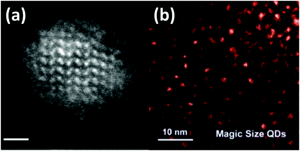 | ||
| Fig. 11 STEM images of (a) CdSe nanoclusters with diameter 3 nm (scale bar – 1 nm), reproduced with permission from ref. 130 [T. J. Pennycook, J. R. McBride, S. J. Rosenthal, S. J. Pennycook and S. T. Pantelides, Nano Lett., 2012, 12, 3038–3042], Copyright American Chemical Society, and (b) CdSe nanoclusters grown in dioctylamine, reproduced with permission from ref. 131 [S. Dai, Y. S. Su, S. R. Chung, K. W. Wang and X. Pan, Nanoscale, 2018, 10, 10256–10261]. Copyright Royal Society of Chemistry. | ||
Overall, it is evident that optical spectroscopy techniques are primarily useful for the characterization of CdSe MSNCs, while other techniques such as XRD, TEM, and mass spectroscopy may provide supporting data.
4. Doping of CdSe MSNCs
The desire to obtain the optimum synergistic blend of quantum confinement effects with traditional doping or creation of hetero-junctions has been the ultimate driving factor for doping semiconductor nanoclusters. Intentional doping of a foreign atom or ion in such nanoclusters provides an additional advantage in controlling the material properties.132–134 This led to the development of diluted magnetic semiconductor nanoclusters where the resultant unique magnetic and electronic properties were attributed to spin exchange interactions between host charge carriers and dopants. Characteristically, the absorption of impurities on the growing nano-cluster surface is said to induce doping. Since this procedure entails a specific particle size for the absorption of dopants, typically there are only minimal chances of doping a MSNC with a dopant ion.135Introducing a transition-metal ion dopant into a semiconductor host usually creates a dopant-related energy level within the bandgap region of the host semiconductor compound. Such mid-gap states induce massive alterations in the properties depending on the nature of these mid-gap states, ultimately determining the properties exhibited by a doped semiconductor nano-cluster.136,137
Extensive studies concerning doped semiconductor nano-crystals with localized states led to fine-tuning of the optical properties. It has been perceived that with the absorption of a photon having an energy higher than the host's bandgap, an electron–hole pair is formed in the host nanocrystal. Due to the enhancement in wave function overlap arising from confining within the QD, there is an increase in the Coulomb attraction between the hole and photo-excited electron, which possess a higher tendency to form an exciton in comparison to the bulk. Consequential electron hole recombination occurs within the dopant sites with the emission of light characteristic of the dopant when there is transfer of energy from this bound state (exciton) to the dopant levels.133 Alternatively, transfer of only the hole or electron to the dopant site can take place, resulting in charge transfer. In this scenario, recombination occurs concerning both the host and the dopant state and hence is also dopant influenced.
It has been realised that upon doping, e.g. manganese, there is a lifting of the degeneracy of excitonic states due to Zeeman splitting, which arises from the dopant's unpaired d electrons when the energy required for excitation is less than the internal d-d transition energy of the d-element dopant. As a result of this, multiple lines in the excitonic emission were seen.138 There are four vital aspects of combination in the synthesis of doped nano-crystals to be looked upon, which provide an outlook of varied metal ion doping. These are doping of magnetic ions in dilute magnetic semiconducting (DMS) NCs, exciton dissociation via dopant states, electron–hole recombination via dopant states, and hole or electron doping with hetero-valent ions. In general, doping is relatively easy to attain when the dopant ion has a size comparable to that of the substituted host ion. Typically, dopant ions induce strain in the host crystal lattice due to dissimilarity in size, which can partially be overcome by thermal annealing.139 Dopants can also affect the catalytic140 as well as photovoltaic141 performance as they affect the photo-generated exciton dissociation.
A vital aspect concerning metal clusters as tailored dopant sources is that these can be synthesized in pure non-metallic configurations as well as in poly-metallic alloy form.142,143 This provides an advantage for doping via directly incorporating various metal impurities in semiconductor hosts. Herein, the type of doping can be tuned by carefully choosing the time point of the reaction at which the dopant impurities are added.144 Based on this, three types of doping are distinguished, namely nucleation,145–151 cation exchange148,152 and growth doping.145,150,153,154
As seen in the case of silver doped CdSe QDs, cation exchange between doped precursors and undoped QDs can be done following the inverted route. In such a way, final doped systems are attained by unfinished substitution of the silver atoms with atoms of cadmium, leaving the inner core of the QDs doped with residual impurities of silver.155 Diffusion doping, which is advantageous over cation exchange as there is no loss of host cations, has been seen to effectively incorporate more considerable amounts of manganese ions in CdSe.156,157 DMS quantum dots having uniformity in the spatial distribution of impurities have gone a long way in addressing the magnetic nature in doping.158
The doping of QDs occurs at an ensemble level producing a Poisson distribution of dopants across the QD population. In order to regulate the behaviour of QD devices, it would be imperative to realize monodisperse ensembles with individual doping possessing a similar number of impurity atoms enabling one to examine dopant-host and dopant-dopant interactions.159,160 This aspect would also help in regulating the nature and efficiency of inter gap state transistors and solar cells as their behaviour depends on precisely tuning the impurity states like the number of unpaired spins or width of the impurity level.161,162 Jawaid et al.147 used [Na(H2O)3]2[Cu4(SPh)6] in order to grow Cu doped CdSe QDs, suggesting that across the QD ensemble monodisperse doping levels could be attained.
The synthesis of doped CdSe MSNCs is primarily conducted with typical solution chemistry methods. Yang et al.135 achieved the smallest Mn2+ doped (CdSe)13 clusters as compared to other researchers by a reaction of selenocarbamate with CdCl2 and MnCl2 in octylamine. This strategy, based on a Lewis acid–base reaction between the metal halide amine complex and Se, resulted in two kinds of Mn2+ doped CdSe clusters capped with octylamine, one with 7.7% and one with 15.4% Mn2+ doping concentration, respectively.163,164 It was also seen that the molar ratios of clusters in the solution relied on the concentration of Mn2+. Successful doping was further confirmed by the observation of absorption peak shifting by 43 meV when increasing the doping concentration from 0 to 10%. The decay curve for clusters with 7% doping concentration followed a double exponential with lifetimes of τ1 = 23 μs and τ2 = 143 μs. In contrast, a single exponential decay was seen for clusters doped with 10% Mn2+. These findings point towards slower decay rates for Cd12MnSe13. The reduction in the decay time with an increase in Mn2+ concentration indicates a partial lifting of the spin selection rules. In line with this, the QY of Cd11Mn2Se13 also decreased from 10 to 6% with an increase in the average doping concentration from 4 to 10%.165
Beatriz et al. and several other groups57,166–168 proposed a quantized approach for doping employing a pre-tuned dopant source, extending the potential of the classical approach for doping. This not only increased the compatibility of synthesis practices with aqueous solvents and environmental factors but was also advantageous and went a long way in realizing the direct applicability of quantum dots for biological and sensing applications. Specifically, metal quantum clusters were employed, which consisted of a core of copper atoms bound with each other by strong metal–metal bonds, to pre-tune the doping at the single-particle level. Thus, groups of doped QDs with the same predetermined number of impurity atoms were obtained.
In another interesting study, Yang et al.169 reported the doping and transformation of multi-element MSNCs producing the smallest alloyed semiconductor cluster ZnxCd13−xSe13 (x = 0–13), employing Lewis acid–base reactions at room temperature. The composition of the so-prepared alloy clusters could be completely regulated from pure cadmium selenide to pure zinc selenide, allowing wide range bandgap control. With the introduction of manganese ions, small-size DMS alloys exhibiting enormous magneto-optical responses in the highest regime have been reported. The formation of alloys in pre-nucleation clusters was amazingly at a very low temperature in comparison to II–VI semiconductor alloys where metal halide amine complexes react with octyl ammonium selenocarbamate in n-octylamine. Herein, the high reactivity of the Se precursor allowed the reaction to proceed at 20 °C. Such low temperature also prevented undesired much higher temperatures of around 250 °C.170 The typical ratio of Zn to Cd in the resulting products was seen to be comparable to that of the precursors used due to the higher reactivity of Se. The preliminary stages saw absorption characteristics from the zinc 34 cluster, which eventually got reduced and ultimately vanished with the zinc 13 cluster band-edge transition becoming clear. This trend of growth was also observed with CdSe clusters as (CdSe)34 → (CdSe)13 proposing a similar mechanism of growth for those (CdSe)13 clusters.138 Upon inspection by optical spectroscopy of the electronic structure of manganese doped (CdSe)13, it was seen that the absorption spectra showed a significant blue shift with band-edge excitonic transitions around 350 nm. An internal Mn2+ transition was also accredited with emission at 600 nm. Energy transfer from the host band state of the semiconductor to states of Mn2+ was confirmed on the basis of the photoluminescence emission (PLE) spectrum, making it obvious that the manganese ions were present in a Cd2+ site.171
Laser desorption/ionization time-of-flight mass spectroscopy was employed for characterizing the prepared clusters. It was observed that the obtained mass spectra exhibited more peaks than the spectra obtained for CdSe and ZnSe, which had only one prominent peak.171,172 A single singularity in the resulting cluster was also observed as different size clusters were not present. It was also interpreted that these alloy clusters were formed by integrating zinc atoms instead of similar cadmium atoms or vice-versa.137 On examining the electronic structure with optical spectroscopy, the absorption edge was predicted to shift towards high energies with the increase in zinc content as the bandgap for bulk ZnSe surpasses that of bulk CdSe with ∼1 eV. The absorption features were comparable and existed between the energy positions of the (ZnSe)13 and (CdSe)13 clusters with the excitonic transitions being shifted continuously from cadmium clusters to zinc clusters when the typical ratio of zinc in the clusters was increased from 0 to 100%. Additionally, absorption spectra depending on the temperature showed a monotonic red shift with an increase in temperature.137
Overall, doping of CdSe nanoclusters with suitable dopants may alter their emission properties, i.e., a shift in emission wavelength, an increase in QY, and variation of the colour temperature along with an increase in the colour rendering index (CRI) when applied in LED devices. Thus, it may be interesting to explore the potential effects of various dopants on the optical properties of CdSe MSNCs after doping.
5. Application of CdSe MSNCs
CdSe MSNCs find a wide range of applications in physics as well as in biology such as fluorescent probes, laser diodes, solar cells, biological labelling, studying in vivo cell migration markers and intracellular imaging (Fig. 12). It has already been reported that rigid particles of a hydrodynamic diameter less than 5.5 nm can be cleared out by the kidneys and hence the ultrasmall size of MSNCs becomes a key feature for application in biological systems.173 MSNCs’ fixed small size, thermal stability, broad emission spectra, high molar absorptivity and fluorescence quantum efficiency are the factors favouring their use in biological systems. For application in biological systems, the monodispersity, size, concentration, capping ligand and stability must be considered as they affect their toxicity. Silva et al.109 showed long-lasting fluorescence in HeLa cells using thioglycerol capped CdSe MSNCs indicating their potential in studies of migration of tumor cells in vivo and intracellular protein trafficking. They have also shown good resistance to photobleaching. Further, in another report, they have done biological analysis of CdSe/CdSxSe1−x/CdS core–shell magic sized nanoclusters and succeeded in coupling the Fab antibody, which can recognize conformational cytokeratin-10 epitope present in the cytosol of breast cancer lines.174 These are promising results, yet further research efforts are deemed necessary in order to address and overcome possible limitations and barriers. These include the chemical toxicity of Cd-based compounds and the need to shift the excitation and emission wavelengths into the biological transparency window.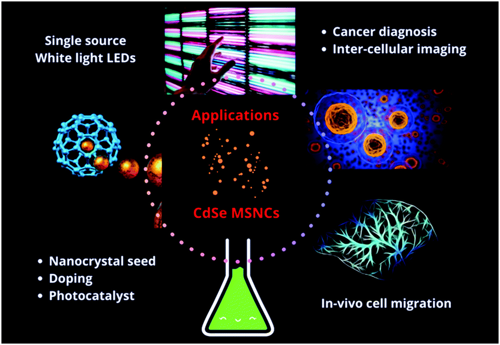 | ||
| Fig. 12 Schematic representation showing diverse applications of CdSe MSNCs. | ||
In its nano-crystalline form, CdSe is of great optoelectronic interest as its bandgap can be tuned across the visible spectral region by varying its particle size. Out of this emerged, for instance, light emitting devices based on II–VI quantum dots and MSNCs. The subsequent sections will discuss these in more detail. In order to explore many other applications of magic sized CdSe MSNCs, they have been used as building-blocks towards larger nano-scale assemblies, such as nanorods, tetrapods, rice-shaped nano-crystals, nano-belts or nano-platelets as presented in Fig. 13.86,124,175,176 In addition, self-assembly with preferred growth directions is a viable approach for the development of nanostructures with well-defined thickness and nano-platelet shapes.177 Nano-crystal seeds have been explored for water splitting and their suitable performance for photocatalysis regarding the quantum efficiency has been demonstrated.172 Amirav et al.178 described semiconductor nano-rods with a platinum tip, which was surrounded by a CdSe seed for its utility as a photocatalyst. With the creation of an electron–hole pair in the CdSe seed, the electron gets drawn to the platinum tip and the hole gets confined to the seed. This assembly provided various advantages in comparison to other photocatalysts. In view of immense energy applications, it is now appropriate to consider first the light emitting diode properties of CdSe quantum dots and then the special photonic properties of CdSe MSNCs for white light applications.
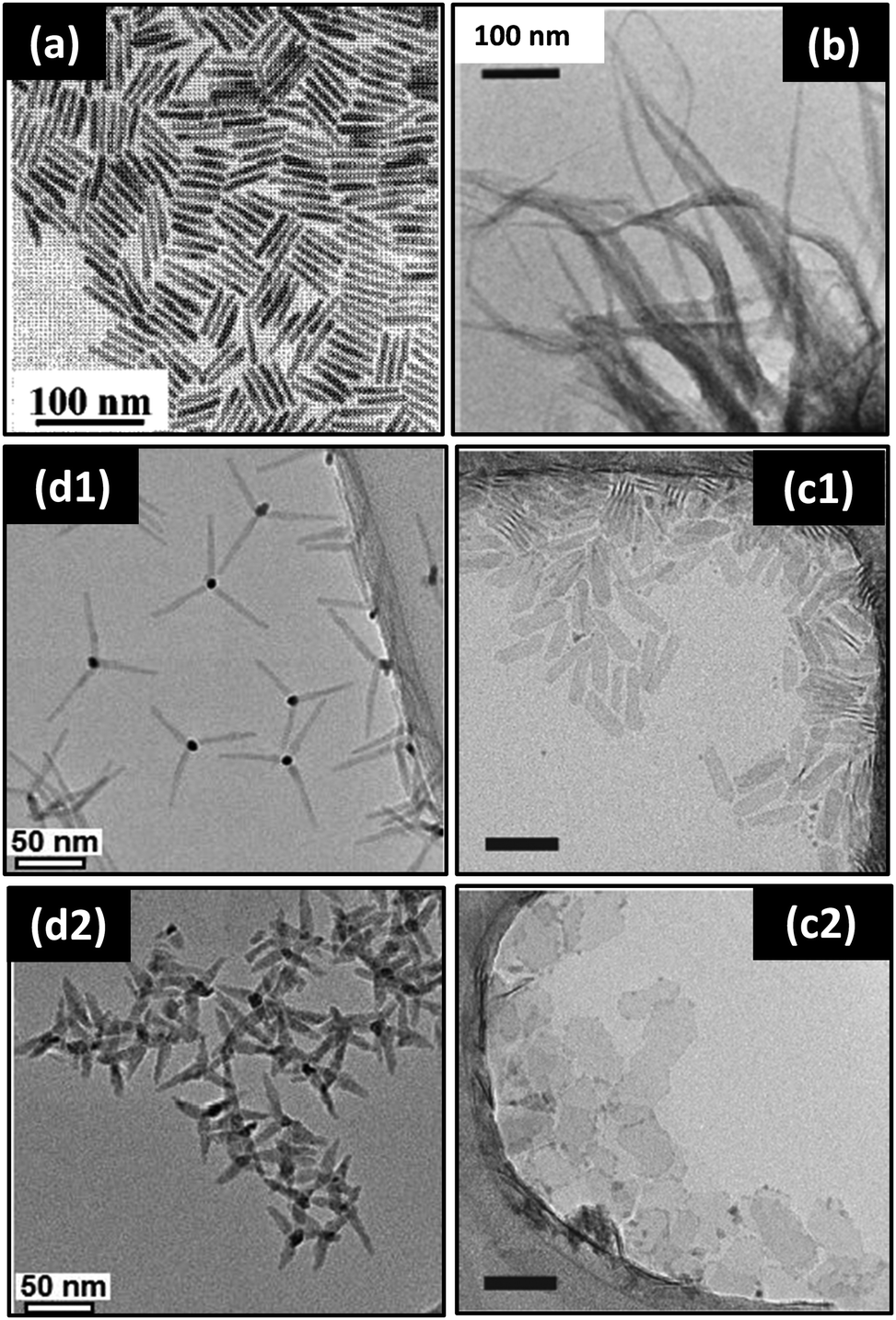 | ||
| Fig. 13 TEM images showing various nanostructures obtained upon assembly of CdSe MSNCs: (a) nanorods, reprinted with permission from ref. 86 [Z.A. Peng, and X. Peng, J. Am. Chem. Soc. 2002, 124, 3343–3353], (b) nanobelts, reprinted with permission from ref. 124 [Y.-H. Liu, F. Wang, Y. Wang, P.C. Gibbons and W.E. Buhro, J. Am. Chem. Soc., 2011, 133, 17005–17013], (c) nanoplates (scale bar 50 nm), reprinted with permission from ref. 175 [S. Ithurria, G. Bousquet and B. Dubertret, J. Am. Chem. Soc., 2011, 133, 3070–3077], and (d) tetrapods, reprinted with permission from ref. 176 [M. J. Enright, F. Y. Dou, S. Wu, E. J. Rabe, M. Monahan, M. R. Friedfeld, C. W. Schlenker and B. M. Cossairt, Chem. Mater., 2020, 32, 4774–4784]. Copyright American Chemical Society. | ||
5.1. CdSe quantum dot-based LEDs (QLEDs)
Light emitting diodes (LEDs) are semiconducting lighting devices, where light is emitted in response to an electrical current or an electrical field, a phenomenon known as electroluminescence. The process behind electroluminescence is radiative recombination, also known as spontaneous emission. An LED device typically consists of a p–n junction layer sandwiched between the anode and cathode. When current flows under forward bias, the charge carriers move toward the p–n junction, where the n-type material donates its extra electrons. These electrons combine with holes, ultimately generating photons. In an LED device, the n/p-type material is chosen such that the energy of the photons falls within the visible region. Oleg Vladimirovich Losev,179 the inventor of LEDs, designated this emission process as the “inverse photoelectric effect”. III–V semiconductors such as gallium arsenide (GaAs), gallium phosphide (GaP), or gallium arsenide phosphide (GaAsP) are popular semiconductors used for LED manufacturing. The combination of various semiconductor materials with a desired adultrant may result in fabrication of LEDs emitting different colours. At the same time, by selecting suitable semiconductor materials, single-colour LEDs can be designed that emit light in a narrow band of wavelengths from the ultraviolet via the visible to the near-infrared region. LEDs have much superiority over incandescent light sources, including low energy consumption, longer lifetime, better robustness, compact size, and fast switching. However, the operating voltage of the LED increases for shorter wavelengths. LEDs are useful in aviation lighting, automotive lights, advertising, domestic lighting, camera flashes, and electrical and medical devices.180 Organic light emitting diodes (OLEDs) instead utilize organic compounds or conjugated polymers as the emissive layers. Hence, these are more environment friendly and flexible but are expensive as compared to inorganic emissive compounds. Moreover, organic semiconductors are prone to oxidation as compared to inorganic counterparts, thereby reducing their lifespan.The tunable bandgap and high emission (PL) quantum efficiency in CdSe QDs make them highly advantageous for LED applications. The wide absorption range and extremely narrow spectral bandwidth of QDs offer high colour purity in LED displays. As inorganic QDs are thermally stable and less prone to oxidation upon exposure to air, it makes them more durable for use in displays. Their easy solution processability facilitates better device fabrication on glass and plastic substrates, hence opening avenues for flexible electronics. QD-based LEDs (QLEDs) also offer a low turn-on voltage, high brightness, wide colour gamut, ultrathin form, lightness and flexibility, which give them great potential for future electronics. A QLED-based device structure is very similar to that of OLEDs where the organic emissive layer is replaced by layers of QDs. The QLED device structure has the following components: (i) a substrate layer which provides support to the QLED device, which can be made of transparent glass or plastic, (ii) an anode which removes electrons or injects holes into a hole transport layer (HTL), (iii) the HTL, which injects holes into the QD layer, (iv) an emissive layer that is composed of mono or a few layers of QDs, (v) an electron transport layer (ETL) that transports electrons from the cathode in the QD layer, (v) a cathode, and sometimes an additional hole blocking layer (HBL). In the given layer the injected charge carriers radiatively recombine and emit light in the visible region. Commonly used organic HTLs are conductive polymers like poly(3,4-ethylendioxythiophene):poly-(styrenesulfonate) (PEDOT:PSS),31,181 4,4′-bis(carbazol-9-yl)biphenyl (CBP),182,183 bis(3-methylphenyl)-N,N′-bis(phenyl)benzidine (TPD),31 polystyrene (PS)-N,N′-diphenyl-N,N′-bis(4-n-butylphenyl)-(1,1′-biphenyl)-4,4′-diamine (TPD) perfluorocyclobutane (PFCB),184 poly[(9,9-dioctylfluorenyl-2,7-diyl)-co-(4,4-(N-(4-sec-butylphenyl))diphenylamine)] (TFB),185etc. Some of the inorganic HTLs are MoO3.182,183 Inorganic ETLs use LiF,181 and ZnO nanoparticles,183,186–189 and a few examples of organic ETLs are 1,3,5-tris(N-phenylbenzimidazol-2-yl)benzene (TPBI), and tris(8-hydroxyquinoline) (Alq3), among others. Using NPs as the ETL solves the problem of QD degradation due to deposition methods as NPs are solution processable and do not require harsh conditions. Also, the use of NPs promises ultrathin CTL layers resulting in an even more compact QLED structure. As anode materials, Al, Ca/Ag, and Mg/Ag have been used, while indium tin oxide (ITO) is the most common material to be used as the cathode. 3,4,5-Triphenyl-1,2,4-triazole (TAZ) has been used as the HBL.190 A typical device structure is presented in Fig. 14(a), while Fig. 14(b) shows its working principle.191
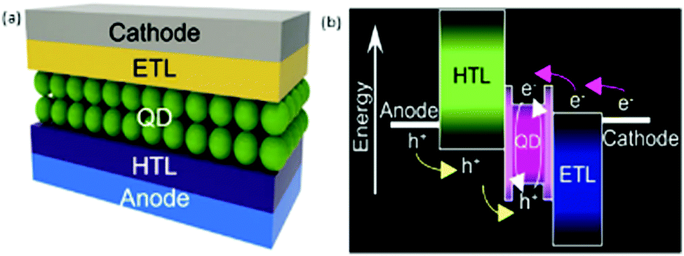 | ||
| Fig. 14 (a) General LED device structure of a QLED and (b) schematic representation of the energy levels of the QDs, HTL and ETL showing the charge transport and recombination. Reproduced with permission from ref. 191 [M. K. Choi, J. Yang, T. Hyeon and D.-H. Kim, Npj Flex. Electron., 2018, 2, 10]. Copyright Springer Nature. | ||
The performance of QLEDs is highly dependent on the chemical composition, size and size distribution, number of layers, surface properties and processing conditions of the QDs. In general, lower efficiency and stability of the device are primarily due to (i) dependency of QD properties such as the photoluminescence quantum yield (PLQY) on the organic ligands, (ii) degradation of the organic ligands during the processing of QD sites, (iii) the presence of non-radiative recombination processes, mostly Auger recombination, and (iv) dot to dot energy transfer.
When QDs are injected with multiple electrons and holes, they become charged and electron–hole pairs recombine non-radiatively, rendering the QDs inactive, resulting in heat generation only. The device efficiency increases with increasing QD coverage until a monolayer (ML) of dots has been deposited. Consequently, QLEDs have the best performance with thickness close to a monolayer. However, the optimal thickness of the QD layer varies for different coloured QLEDs as it depends on the size and structure of the QDs. The use of thinner QD layers minimises the effect of Auger recombination in charged QDs and slows the QD-to-QD energy transfer. But a monlayer (ML) thin film may not perform optimally either. This is due to the higher probability of the presence of voids, interstitial spaces and grain boundaries in monolayers, which risks increased leakage current through the QD layer. Although ML QDs offer a lower turn-on voltage and higher efficiency, their luminance and colour purity are hindered due to poor confinement of excitons inside the QD and low quantity of the chromophore. Core/shell QDs where a wide bandgap material overcoats the core are known to improve the performance of a device. The wide bandgap shell has two advantages: (i) protecting the core from surface defects which may appear during deposition of the QD layer, and (ii) confining the excitons to the core, which leads to higher external quantum efficiency (EQE).
Araki et al.192 have demonstrated CdSe QDs as a promising material for green light emission by fabricating green LEDs using CdSe QDs as emission layers. They observed an emission wavelength of 530 nm at a current of 20 mA with CdSe as an emissive layer and ZnSe as an intermediate layer. Firth et al.193 synthesized new polymers with pendant phosphine or phosphine oxide groups for size quantization of CdSe from the reaction of Me2Cd with H2Se to yield CdSe nanoparticles. They observed that, for smaller particles, the energy and profile of the emission band (QY up to 45%) were independent of the particle size and the broad luminescence pattern was close to white light emission. Based on the results, they suggested the use of CdSe in white light LEDs via stimulation from blue LEDs. CdSe/ZnS core/shell QDs exhibit a high PLQY of 70–95%, which is several orders higher than that of bare QDs. There are several reports on using core/shell QDs which exhibit high QLED performance. For instance, Zhao et al.184 synthesized CdSe/CdS QLEDs with spectrally pure emission and no background emission from the organic polymer. Sun et al.194 took CdSe as the core overcoated by a ZnS single shell or CdS/ZnS double shell. Controlling the size and structure of the core and shell yielded green, yellow, orange and red QDs with a narrow emission bandwidth (FWHM 20–30 nm). The QY of the as-prepared colloidal QDs was more than 70%. However, the fluorescence QY for the QDs was reduced to 10, 30, 40 and 35% for green, yellow, orange and red QDs after purification. During the purification step of the QDs to be applied in QLEDs, organic ligands are removed from the surface, producing surface defects which may trap charges. The smaller the QD size, the larger the surface area, and hence the more pronounced the surface defects. Therefore, the highest reduction in QY was observed in the case of green QDs. The QLEDs fabricated had a turn-on voltage of 3–4 V. The achieved maximum luminance and luminous efficiency values, respectively, were 9064 cd m−2 and 2.8 cd A−1 for the red device, 3200 cd m−2 and 1.8 cd A−1 for the orange device, 4470 cd m−2 and 1.3 cd A−1 for the yellow device, and 3700 cd m−2 and 1.1 cd A−1 for the green device. Higher QY does not guarantee higher electroluminescence (EL) performance; Auger non-radiative recombination or dot to dot energy transfer may reduce the efficiency. These factors are greatly dependent on the core/shell interfaces and hence there are many studies to understand the process occurring and modify these interfaces.182 One way to do this is to modify the thickness of the shell, which inhibits fluorescence intermittency or blinking and eliminates photobleaching, inducing long-term stability. QLEDs utilizing CdSe/ZnS core/shell structures have reached an EQE (external quantum efficiency) of 3%.194,195
Pal et al.181 studied the effect of changing the thickness of the ZnS shell on the properties of CdSe/CdS QLEDs. The shells were 4, 8, 11, 13 and 16 ML thick. A turn-on voltage of 3 V and maximum luminance of 2000 Cd/m2 at a current density (J) of 1.2 A/cm2 and voltage of 11 V were achieved from the 16 ML thick shell, offering the best results among all the samples. The QDs with thick shells (11–16 ML) have shown a higher EQE and maximum luminance than their thinner counterparts. The maximum luminance and EQE of these thick shell QDs when compared to previously reported thin-shell CdSe/CdS–ZnS QDs (two MLs each of CdS and ZnS) having a high PL QY of ∼70% were found to be superior. Unfortunately, these devices degraded completely after operating for a few minutes. There are also some disadvantages of using thick shell quantum dots. (i) Encapsulation with wider bandgap semiconductor materials leads to a reduction in the effective bandgap of the QDs. (ii) The density of QDs is effectively reduced in the layer as the core/shell size is much larger than that of core-only QDs. (iii) The wide bandgap semiconductor shell may inhibit injection of electrons and raise the QLED turn-on voltage. The performance of QLEDs is also dependent on the charge transport layer (CTL). The higher the carrier mobility, the better the CTL. Also, it should balance the electron/hole injection. The CTL can be an organic, inorganic or hybrid material. Organic CTLs often exhibit background luminescence; therefore, organic polymers must be chosen carefully. Inorganic materials are the most promising choice among these due to their high electrical conductivity and their robust nature towards environmental factors. The use of an inorganic CTL enables long term usage and high current density conditions, but the deposition process of these inorganic materials requires harsh conditions which can cause degradation of the QDs. Making use of the superior characteristics of both types of CTLs, hybrid structures seem to be a favourable approach.10
5.2. White light emission from CdSe MSNCs
LEDs are already a solid-state frontier where energy-saving white LEDs hold much significance. MSNCs are potentially excellent candidates for applications in white LEDs, showing the right equilibrium of emission to produce almost pure white light according to CIE coordinates (0.31, 0.33),14,68,85,116,117,196 while MSNCs of CdSe have been evaluated for their characteristic to emit white light.30,105,110,197–199 MSNCs can work as a single source white light emitter, which has several advantages over hybrid LEDs with mixed red, green and blue phosphors. These advantages are generally in terms of cost, durability, energy-saving, customization, and better colour retention.Despite these challenges, recent efforts have been undertaken by several research groups around the globe resulting in highly promising CdSe MSNC-based phosphors with proven potential for application as white light emitting LEDs. For instance, Bowers and co-workers proposed pyrolytically synthesized CdSe MSNCs as a potential white light emitting phosphor, based on an emission profile covering the entire visible spectrum in addition to exhibiting a large Stokes shift.199 These properties were ascribed to the surface to volume ratio, promoting the interaction of holes and electrons on the surface of the nano-crystals, ultimately yielding white light emission. Generally, in ultra-small nano-crystals, deep trap emission is common, which is accompanied by large band edge emission. Consequently, a reduction in the quality of the produced white light, i.e., emission biased towards a specific colour, was observed in the presence of this resilient band edge. Overall, upon optimization of their CdSe MSNCs, a white-light emitting material having chromaticity coordinates of (0.322, 0.365) was achieved, which was in good agreement with the 1931 CIE diagram's white region. The colour quality based on the CRI and CIE coordinates of white light emitting CdSe-based LEDs was further studied by Gosnell et al.198 The studied LEDs had good white colour quality with CRI > 80 and CIE coordinates near pure white light. As a critical finding, the authors concluded that an extremely thin film might result in pure white light emission.
Schreuder et al.166,197 incorporated CdSe nanoclusters into photoluminescent and electroluminescent solid-state devices. Therefore, CdSe MSNCs were encapsulated in a polymer matrix, and the obtained hybrid layer was arranged on top of a UV LED. The chosen polymer was demonstrated as highly suitable as it did not have any adverse effect on the white light spectrum of the nanoclusters. Liu et al.30 synthesized CdSe MSNCs and obtained a 392 family by passivating the surface with a long chain fatty acid. These CdSe MSNCs displayed strong white light emission with a QY of more than 25%. The broad emission spanning the spectral region from 370 to 680 nm resulted in overall white emission and was accredited to exciton and surface state photoluminescence.
Furthermore, the microwave-assisted synthesis of CdSe MSNCs for white light applications by using an organometallic compound i.e. 1,2,3-selenadiazole and oleic acid as a capping agent has been reported.40 The specific use of 1,2,3-selenadiazole and oleic acid was vital to obtain CdSe MSNCs. It was observed that the white light emission was a net result of the radiative recombination from the surface and the core states of these MSNCs. Photoluminescence decay studies revealed both fast and slow recombination rates within the MSNCs, prompting their broad emission profile. The broad emission profile leading to white light was ascribed to un-coordinated surface Se atoms and mid-gap defects within the clusters. The same group further reported similar white light emission from CdSe MSNCs capped with edible oils instead of oleic acid. For instance, CdSe MSNCs capped with mustard oil exclusively delivered white light. Remarkably, these phosphors were found to be stable with unaltered emission behaviour for more than a year.105 The CIE diagram for white light emission (colour temperature: 7063 K; CIE 2015 coordinates: x − 0.3059, y − 0.3161) corresponded to light summer shade (Fig. 15b). Among the various synthesis approaches suitable for CdSe MSNCs, phosphors obtained by aqueous approaches were also demonstrated to be white light emitting candidates. For example, pure white light emission from CdSe nanoclusters synthesized in aqueous medium employing 3-mercaptopropionic acid (MPA) as a capping agent was reported by More et al.106 The authors ascribed the observed white light emission to two mechanisms, namely deep trap emission from surface Se–S bonds between MPA and MSNCs and shallow traps from uncoordinated Se atoms on the surfaces of MSNCs. Additionally, it was shown that higher Cd concentration in the CdSe nanoclusters delivered brighter white light (Fig. 15c inset).
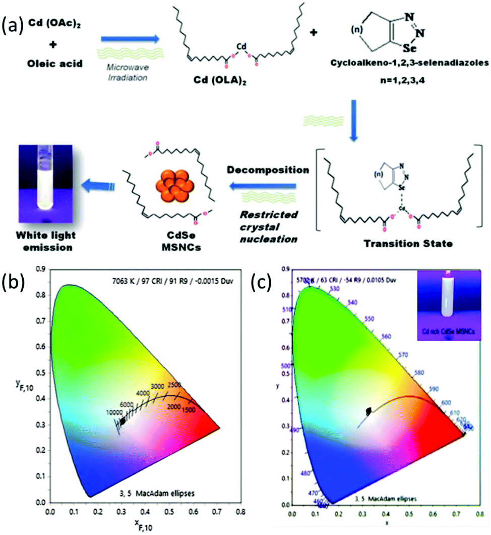 | ||
| Fig. 15 (a) Schematic representation of the synthesis of white light emitting CdSe MSNCs with an inset image of a sample showing white light emission under 365 nm UV-light exposure and various selenadiazoles used for synthesis of MSNCs. Reproduced with permission from ref. 104 [A. A. Jadhav, P. V. More and P. K. Khanna, RSC Adv. 2015, 5, 76733–76742]. Copyright Royal Society of Chemistry. (b) CIE (1931) diagram plot for mustard oil-capped CdSe MSNCs showing a colour temperature of 7063 and light summer (white) shade. Reproduced with permission from ref. 105 [P. K. Khanna, A. Jadhav and P. V. More, J. Nanosci. Nanotechnol., 2020, 20, 2946–2954]. (c) CIE (1931) diagram plot for Cd-rich CdSe MSNCs capped with 3-mercaptopropionic acid (colour temperature: 4030 K; CIE coordinates, x − 0.377 and y − 0.3677); inset, white light emission in water upon UV (365 nm) lamp excitation. Reproduced with permission from ref. 106 [P. V. More, C. B. Hiragond, A. Jadhav, P. Kush, S. Sapra and P. K. Khanna, Chem. Select. 2017, 2, 11775–11782]. Copyright Wiley. | ||
Thus, CdSe MSNCs can serve as a single source material for white light emission, which can be highly advantageous as compared to traditional phosphors and QDs. The next aim in this perspective would be the implementation of MSNCs into devices followed by a critical assessment of their performance. There are extremely few reports of white LED devices fabricated using TOP capped CdSe MSNCs as emissive layers. Gosnell et al.200 were the first to report the potential of CdSe MSNCs in white light emitting devices. These CdSe MSNCs (size <1.5 nm) with an absorption band feature at 414 nm were encapsulated in perfluorocyclobutyl (PFCB) polymer with varied concentrations (2–10%) to study its effect on the optical properties. These CdSe/PFCB assemblies were aligned in combination with commercial blue LEDs to produce various shades of white light, which could be tuned from a cooler to a warmer white by increasing the concentration of nano-crystals in the PFCB polymer. Recently, Sadeghi et al.201 reported a prototype white LED using liquid-state TOP capped CdSe MSNCs with a CRI up to 89 and luminous efficiency of 11.7 lm/W. They fabricated a unique LED device using a blue chip attached to a cured PDMS lens that was coated with the white-emitting MSNCs. Another exciting report by Dai et al.202 demonstrates white LEDs using TOP capped CdSe nano-crystals. An InGaN/GaN-based near-UV emitting LED device was fabricated by using a 3020 surface-mounted device (SMD). The CdSe nano-crystals and thermally cured epoxy gel were packed at room temperature for about 6 h to form a white LED device. The fabricated white LED devices with CdSe nano-crystals delivered desirable properties, such as a high CRI value (77–89), improved efficacy (0.3–2 lm/W) and ideal CCT values (∼3600–8350 K). Fig. 16 shows the characteristics of an LED made of white emitting CdSe QDs at different values of the supplied current along with the CRI and luminous intensity. Overall, while recent work demonstrates the feasibility and suitability of CdSe MSNCs for white LEDs, this promising field is still considered in its infancy and there exists a need for further exploration.
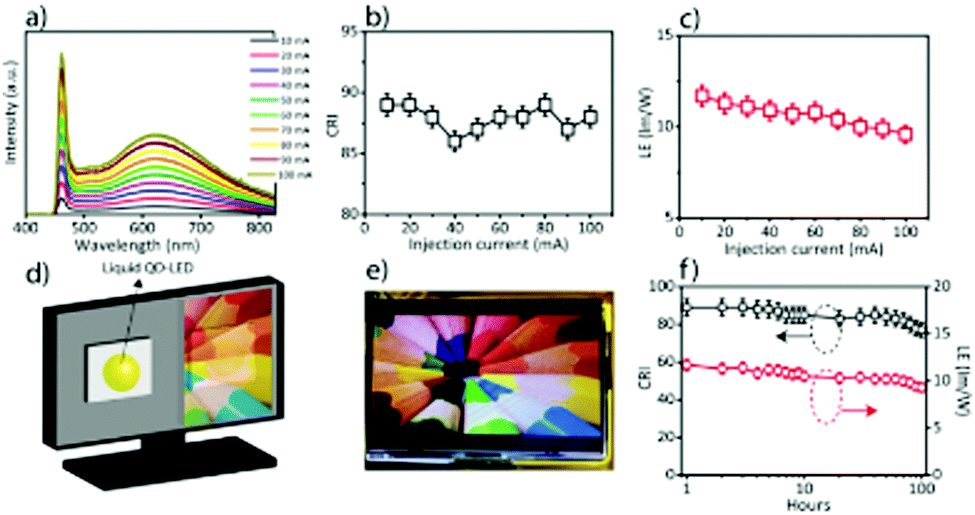 | ||
| Fig. 16 (a) The generated white light spectrum at different current levels ranging from 10 mA to 100 mA. (b) Colour rendering index (CRI) and (c) the luminous efficiency (LE) at different current levels. (d) The schematic of a 7-inch LCD display being illuminated with two magic-sized QD based white LEDs. (e) The photograph of an image generated by the 7-inch LCD display. (f) The optical stability of a magic-sized CdSe QD based white LED during 100 h. Reproduced with permission from ref. 201 [S. Sadeghi, S. Khabbaz Abkenar, C. W. Ow-Yang and S. Nizamoglu, Sci. Rep., 2019, 9, 10061]. Copyright Springer Nature. | ||
6. Conclusion
In conclusion, there is an obvious and enormous curiosity in developing white-light emitting materials for solid state lighting. Yet, commercially available white LEDs these days rely on complicated fabrication methods. Thus, employing magic-sized, white light emitting CdSe nano-crystals as a direct white light phosphor has great potential to eliminate the requirement for complex doping schemes and deposition techniques. Despite their promise, challenges remain in the synthesis of such clusters. Importantly, although there have been rigorous studies in the past years, no consensus could be established to date regarding the most precise synthesis methods, structure and composition of CdSe MSNCs. To develop this understanding, it would require more in-depth studies on the reaction kinetics of their formation, which would allow practical access to these sub-2 nm particles.It is noteworthy that the establishment of CdO as a substitute for conventional Cd precursors provided great insights into synthesis. Besides CdO, Cd-based fatty acid complexes have been demonstrated as more suitable cadmium precursors than dimethyl cadmium.113,203 It is also observed that the source of selenium does matter for maintaining the quality of CdSe MSNCs. Indeed, a 1,2,3-selenadiazole driven synthesis boosts the chemistry of such materials and opens the scope of simple selenium molecules to participate in this high technology field. These two changes in precursor chemistry allowed detailed studies on CdSe MSNCs and gave valuable insights regarding their growth process; however, it would be significant to investigate this regime further. Another important finding was that the variety of bandgap values that are attained during synthesis cannot alone be dependent on the functional group of the ligands used but also on the chain length as well as the reaction temperature as differently sized clusters were obtained using the same functional group ligands. Looking at the literature regarding synthesis, it seems that there exist two main sets of nanoclusters based on the respective synthetic approach, one being fashioned using fatty acid ligands and the other being based on phosphonic acid or phosphinic acid ligands. On the other hand, for synthesis employing carboxylic acid, lower temperatures with short chain fatty acids produced smaller magic-sized nanoclusters, while high temperatures along with long chain fatty acids yielded larger MSNCs. For instance, Yu et al.125 perceived that the size of the clusters formed or whether they will form at all is affected by the degree of super-saturation of the monomer precursor. There was also some argument by the authors that this degree of super-saturation increases with the elevation in reaction temperature or chain length of the fatty acid, eventually resulting in larger MSNCs. It was also realised that with the increase or decrease in the activation barrier, coordinating solvents can have an effect on the yield of the reaction. Other reaction parameters, the variation of which affects the formation of CdSe MSNCs, include the Cd-to-Se ratio, the cluster growth temperature, and the nature of the capping agents.85 It has also been seen that with some experimental conditions MSNCs do not follow quantized growth but rather act as a source of the semiconductor monomer204,205 and in some cases constitute an intermediate for other materials.86,91,126,206,207 CdSe MSNCs are meta-stable compounds but could be destabilized by changing the reaction conditions and quickly decompose with the concentration of the monomer dropping below a certain critical rate, which might cause secondary nucleation.205,207–209 Hence, the balance between MSNCs, nano-crystals and free monomers has to be studied in the near future in order to gain full control over selective growth. Challenges associated with working with such small clusters are the absence of means and methods to characterize them. Using sizing curves from larger nano-crystals based on X-ray diffraction data and transmission electron microscopy compared with UV-vis absorption peaks is the widely accepted way to approximate the size of a nano-crystal of a size below 2 nm in diameter. Optical characterization, particularly UV-vis spectroscopy, which reveals multiple peaks for MSNCs as the characteristic property, is certainly the most used characterization method. The ability to dope these CdSe MSNCs with various dopants may further unravel their unique optical properties with greater stability and spectral identity. The utility of these CdSe MSNCs in LEDs has the potential to offer innovative pathways to power saving, enhanced durability and low-cost devices. Last but not least, due to their distinctive properties, CdSe MSNCs can also be useful in fluorescent probes, laser diodes, catalysis, solar cells, nano-crystal doping and biological labeling.
Conflicts of interest
There are no conflicts to declare.Acknowledgements
The authors thank the SPARC-HMRD programme of the Govt of India for support (Grant No. SPARC/2018-2019/P573/SL) and Vice-Chancellor, DIAT, Pune, for permission. VS thanks Director Rajasthan University for permission to undertake a summer internship at DIAT. VS and Priyanka thank Neha Bisht for her fruitful discussion. The authors thank the Royal Society of Chemistry for their policy to reproduce self-published and also figures from other RSC journal articles. We thank all other publishers also for giving kind permission to reproduce figures wherever mentioned.Notes and references
- J. D. Patterson and B. C. Bailey, Solid State Physics, Springer Berlin Heidelberg, Berlin, Heidelberg, 2007.
- N. Dharmarasu, H. Hillmer and F. T. Mahi, Reference Module in Materials Science and Materials Engineering, Elsevier, 2017 Search PubMed.
- C. Landes, M. Braun, C. Burda and M. A. El-Sayed, Nano Lett., 2001, 1, 667–670 CrossRef CAS.
- A. M. Smith and S. Nie, Acc. Chem. Res., 2010, 43, 190–200 CrossRef CAS.
- S. F. Bent, in Chemical Bonding at Surfaces and Interfaces, eds. A. Nilsson, L. G. M. Pettersson and J. K. Nørskov, Elsevier, Amsterdam, 2008, pp. 323–395 Search PubMed.
- B. P. Isaacoff and K. A. Brown, Nano Lett., 2017, 17, 6508–6510 CrossRef CAS.
- A. P. Alivisatos, Science, 1996, 271, 933–937 CrossRef CAS.
- M. Bruchez Jr, Science, 1998, 281, 2013–2016 CrossRef CAS.
- D. J. Milliron, I. Gur and A. P. Alivisatos, MRS Bull., 2005, 30, 41–44 CrossRef CAS.
- S. Coe, W. K. Woo, M. Bawendi and V. Bulović, Nature, 2002, 420, 800–803 CrossRef CAS.
- V. L. Colvin, M. C. Schlamp and A. P. Alivisatos, Nature, 1994, 370, 354–357 CrossRef CAS.
- T. C. Harman, Science, 2002, 297, 2229–2232 CrossRef CAS.
- M. Carvelli, R. A. J. Janssen and R. Coehoorn, Phys. Rev. B: Condens. Matter Mater. Phys., 2011, 83, 075203 CrossRef.
- D. Katz, T. Wizansky, O. Millo, E. Rothenberg, T. Mokari and U. Banin, Phys. Rev. Lett., 2002, 89, 086801 CrossRef.
- M. Nirmal, C. B. Murray and M. G. Bawendi, Phys. Rev. B: Condens. Matter Mater. Phys., 1994, 50, 2293–2300 CrossRef CAS.
- J. K. Jaiswal, H. Mattoussi, J. M. Mauro and S. M. Simon, Nat. Biotechnol., 2003, 21, 47–51 CrossRef CAS.
- J. B. Delehanty, I. L. Medintz, T. Pons, F. M. Brunel, P. E. Dawson and H. Mattoussi, Bioconjugate Chem., 2006, 17, 920–927 CrossRef CAS.
- H. Mattoussi, J. M. Mauro, E. R. Goldman, T. M. Green, G. P. Anderson, V. C. Sundar and M. G. Bawendi, Phys. Status Solidi B, 2001, 224, 277–283 CrossRef CAS.
- H. Mattoussi, J. M. Mauro, E. R. Goldman, G. P. Anderson, V. C. Sundar, F. V. Mikulec and M. G. Bawendi, J. Am. Chem. Soc., 2000, 122, 12142–12150 CrossRef CAS.
- A. Sukhanova, J. Devy, L. Venteo, H. Kaplan, M. Artemyev, V. Oleinikov, D. Klinov, M. Pluot, J. H. M. Cohen and I. Nabiev, Anal. Biochem., 2004, 324, 60–67 CrossRef CAS.
- M. E. Akerman, W. C. W. Chan, P. Laakkonen, S. N. Bhatia and E. Ruoslahti, Proc. Natl. Acad. Sci., 2002, 99, 12617–12621 CrossRef CAS.
- X. Gao, W. C. W. Chan and S. Nie, J. Biomed. Opt., 2002, 7, 532 CrossRef CAS.
- J. A. Kloepfer, R. E. Mielke, M. S. Wong, K. H. Nealson, G. Stucky and J. L. Nadeau, Appl. Environ. Microbiol., 2003, 69, 4205–4213 CrossRef CAS.
- M. A. Hines and P. Guyot-Sionnest, J. Phys. Chem., 1996, 100, 468–471 CrossRef CAS.
- M. Kuno, J. K. Lee, B. O. Dabbousi, F. V. Mikulec and M. G. Bawendi, J. Chem. Phys., 1997, 106, 9869–9882 CrossRef CAS.
- D. V. Talapin, A. L. Rogach, A. Kornowski, M. Haase and H. Weller, Nano Lett., 2001, 1, 207–211 CrossRef CAS.
- B. O. Dabbousi, J. Rodriguez-Viejo, F. V. Mikulec, J. R. Heine, H. Mattoussi, R. Ober, K. F. Jensen and M. G. Bawendi, J. Phys. Chem. B, 1997, 101, 9463–9475 CrossRef CAS.
- I. Ugarte, I. Castell, E. Palomares and R. Pacios, in Quantum Dots - A Variety of New Applications, ed. A. Al-Ahmadi, Intech, 2012, 6, 115–136 Search PubMed.
- W. C. Chan, Science, 1998, 281, 2016–2018 CrossRef CAS.
- X. Liu, Y. Jiang, C. Wang, S. Li, X. Lan and Y. Chen, Phys. Status Solidi A, 2010, 207, 2472–2477 CrossRef CAS.
- L. Kim, P. O. Anikeeva, S. A. Coe-Sullivan, J. S. Steckel, M. G. Bawendi and V. Bulović, Nano Lett., 2008, 8, 4513–4517 CrossRef CAS.
- A. Kasuya, R. Sivamohan, Y. A. Barnakov, I. M. Dmitruk, T. Nirasawa, V. R. Romanyuk, V. Kumar, S. V. Mamykin, K. Tohji, B. Jeyadevan, K. Shinoda, T. Kudo, O. Terasaki, Z. Liu, R. V. Belosludov, V. Sundararajan and Y. Kawazoe, Nat. Mater., 2004, 3, 99–102 CrossRef CAS.
- I. L. Medintz, S. A. Trammell, H. Mattoussi and J. M. Mauro, J. Am. Chem. Soc., 2004, 126, 30–31 CrossRef CAS.
- S. Kahmann, A. Shulga and M. A. Loi, Adv. Funct. Mater., 2020, 30, 1904174 CrossRef CAS.
- G. Drummen, Int. J. Mol. Sci., 2010, 11, 154–163 CrossRef CAS.
- Y. Wang, Y. Zhou, Y. Zhang and W. E. Buhro, Inorg. Chem., 2015, 54, 1165–1177 CrossRef CAS.
- Z. Wang, X. Teng and C. Lu, Anal. Chem., 2015, 87, 3412–3418 CrossRef CAS.
- M. Omidi, M. Sabzehzari and H. R. Shamlouei, Chin. J. Phys., 2020, 65, 567–578, DOI:10.1016/j.cjph.2020.02.032.
- P. Schwerdtfeger, L. N. Wirz and J. Avery, Wiley Interdiscip. Rev.: Comput. Mol. Sci., 2015, 5, 96–145 CAS.
- A. A. Jadhav and P. K. Khanna, New J. Chem., 2017, 41, 14713–14722 RSC.
- B. Adhikari and A. Banerjee, Chem. Mater., 2010, 22, 4364–4371 CrossRef CAS.
- J. Belloni, Catal. Today, 2006, 113, 141–156 CrossRef CAS.
- X. Le Guével, C. Spies, N. Daum, G. Jung and M. Schneider, Nano Res., 2012, 5, 379–387 CrossRef.
- C. Marambio-Jones and E. M. V. Hoek, J. Nanopart. Res., 2010, 12, 1531–1551 CrossRef CAS.
- J. Zheng, P. R. Nicovich and R. M. Dickson, Annu. Rev. Phys. Chem., 2007, 58, 409–431 CrossRef CAS.
- I. Díez and R. H. A. Ras, Nanoscale, 2011, 3, 1963 RSC.
- H. Xu and K. S. Suslick, ACS Nano, 2010, 4, 3209–3214 CrossRef CAS.
- C. M. Aikens, J. Phys. Chem. Lett., 2011, 2, 99–104 CrossRef CAS.
- W. Lesniak, A. U. Bielinska, K. Sun, K. W. Janczak, X. Shi, J. R. Baker and L. P. Balogh, Nano Lett., 2005, 5, 2123–2130 CrossRef CAS.
- X. Le Guével, B. Hötzer, G. Jung, K. Hollemeyer, V. Trouillet and M. Schneider, J. Phys. Chem. C, 2011, 115, 10955–10963 CrossRef.
- S. S. Narayanan and S. K. Pal, J. Phys. Chem. C, 2008, 112, 4874–4879 CrossRef CAS.
- T. U. B. Rao, B. Nataraju and T. Pradeep, J. Am. Chem. Soc., 2010, 132, 16304–16307 CrossRef CAS.
- T. Udaya Bhaskara Rao and T. Pradeep, Angew. Chem., Int. Ed., 2010, 49, 3925–3929 CrossRef CAS.
- L. Maretti, P. S. Billone, Y. Liu and J. C. Scaiano, J. Am. Chem. Soc., 2009, 131, 13972–13980 CrossRef CAS.
- L. Shang and S. Dong, Chem. Commun., 2008, 1088–1090 RSC.
- T. P. Bigioni, R. L. Whetten and Ö. Dag, J. Phys. Chem. B, 2000, 104, 6983–6986 CrossRef CAS.
- E. E. Lees, T.-L. Nguyen, A. H. A. Clayton and P. Mulvaney, ACS Nano, 2009, 3, 1121–1128 CrossRef CAS.
- T. G. Schaaff, M. N. Shafigullin, J. T. Khoury, I. Vezmar, R. L. Whetten, W. G. Cullen, P. N. First, C. Gutiérrez-Wing, J. Ascensio and M. J. Jose-Yacamán, J. Phys. Chem. B, 1997, 101, 7885–7891 CrossRef CAS.
- Y. Negishi, K. Nobusada and T. Tsukuda, J. Am. Chem. Soc., 2005, 127, 5261–5270 CrossRef CAS.
- S. Chen, Science, 1998, 280, 2098–2101 CrossRef CAS.
- J. F. Hicks, A. C. Templeton, S. Chen, K. M. Sheran, R. Jasti, R. W. Murray, J. Debord, T. G. Schaaff and R. L. Whetten, Anal. Chem., 1999, 71, 3703–3711 CrossRef CAS.
- J. F. Hicks, D. T. Miles and R. W. Murray, J. Am. Chem. Soc., 2002, 124, 13322–13328 CrossRef CAS.
- B. M. Quinn, P. Liljeroth, V. Ruiz, T. Laaksonen and K. Kontturi, J. Am. Chem. Soc., 2003, 125, 6644–6645 CrossRef CAS.
- K. S. Park, M. I. Kim, M.-A. Woo and H. G. Park, Biosens. Bioelectron., 2013, 45, 65–69 CrossRef CAS.
- N. L. Rosi and C. A. Mirkin, Chem. Rev., 2005, 105, 1547–1562 CrossRef CAS.
- C.-A. J. Lin, T.-Y. Yang, C.-H. Lee, S. H. Huang, R. A. Sperling, M. Zanella, J. K. Li, J.-L. Shen, H.-H. Wang, H.-I. Yeh, W. J. Parak and W. H. Chang, ACS Nano, 2009, 3, 395–401 CrossRef CAS.
- F. Wang, W. B. Tan, Y. Zhang, X. Fan and M. Wang, Nanotechnology, 2006, 17, R1–R13 CrossRef CAS.
- Y. Zhou, R. Jiang, Y. Wang, H. W. Rohrs, N. P. Rath and W. E. Buhro, Inorg. Chem., 2019, 58, 1815–1825 CrossRef CAS.
- L.-J. Zhang, X.-C. Shen, H. Liang and J.-T. Yao, J. Phys. Chem. C, 2010, 114, 21921–21927 CrossRef CAS.
- H. Xu, Y. Hou and H. Zhang, J. Nanopart. Res., 2017, 19, 189 CrossRef.
- M. Chen, C. Luan, M. Zhang, N. Rowell, M. Willis, C. Zhang, S. Wang, X. Zhu, H. Fan, W. Huang, K. Yu and B. Liang, J. Phys. Chem. Lett., 2020, 11, 2230–2240 CrossRef CAS.
- C. Luan, Ö. Ö. Gökçinar, N. Rowell, T. Kreouzis, S. Han, M. Zhang, H. Fan and K. Yu, J. Phys. Chem. Lett., 2018, 9, 5288–5295 CrossRef CAS.
- A. D. Dukes, J. R. McBride and S. J. Rosenthal, Chem. Mater., 2010, 22, 6402–6408 CrossRef CAS.
- D. C. Gary, S. E. Flowers, W. Kaminsky, A. Petrone, X. Li and B. M. Cossairt, J. Am. Chem. Soc., 2016, 138, 1510–1513 CrossRef CAS.
- J. Ning and U. Banin, Chem. Commun., 2017, 53, 2626–2629 RSC.
- D. C. Gary, M. W. Terban, S. J. L. Billinge and B. M. Cossairt, Chem. Mater., 2015, 27, 1432–1441 CrossRef CAS.
- Q. Yu and C.-Y. Liu, J. Phys. Chem. C, 2009, 113, 12766–12771 CrossRef CAS.
- P. Khanna, P. More, B. Bharate and A. Vishwanath, J. Lumin., 2010, 130, 18–23 CrossRef CAS.
- Y.-S. Xia and C.-Q. Zhu, Mater. Lett., 2008, 62, 2103–2105 CrossRef.
- K. Yu, J. Ouyang and D. M. Leek, Small, 2011, 7, 2250–2262 CrossRef CAS.
- V. N. Soloviev, A. Eichhöfer, D. Fenske and U. Banin, J. Am. Chem. Soc., 2001, 123, 2354–2364 CrossRef CAS.
- K. Eichkorn and R. Ahlrichs, Chem. Phys. Lett., 1998, 288, 235–242 CrossRef CAS.
- D. Zhu, J. Hui, N. Rowell, Y. Liu, Q. Y. Chen, T. Steegemans, H. Fan, M. Zhang and K. Yu, J. Phys. Chem. Lett., 2018, 9, 2818–2824 CrossRef CAS.
- Y. Negishi, Y. Takasugi, S. Sato, H. Yao, K. Kimura and T. Tsukuda, J. Am. Chem. Soc., 2004, 126, 6518–6519 CrossRef CAS.
- J. Ouyang, M. B. Zaman, F. J. Yan, D. Johnston, G. Li, X. Wu, D. Leek, C. I. Ratcliffe, J. A. Ripmeester and K. Yu, J. Phys. Chem. C, 2008, 112, 13805–13811 CrossRef CAS.
- Z. A. Peng and X. Peng, J. Am. Chem. Soc., 2002, 124, 3343–3353 CrossRef CAS.
- S. M. Harrell, J. R. McBride and S. J. Rosenthal, Chem. Mater., 2013, 25, 1199–1210 CrossRef CAS.
- K. Yu, J. Ouyang, M. B. Zaman, D. Johnston, F. J. Yan, G. Li, C. I. Ratcliffe, D. M. Leek, X. Wu, J. Stupak, Z. Jakubek and D. Whitfield, J. Phys. Chem. C, 2009, 113, 3390–3401 CrossRef CAS.
- R. K. Beri and P. K. Khanna, CrystEngComm, 2010, 12, 2762 RSC.
- R. Beri and P. Khanna, J. Nanosci. Nanotechnol., 2011, 11, 5137–5142 CrossRef CAS.
- S. Kudera, M. Zanella, C. Giannini, A. Rizzo, Y. Li, G. Gigli, R. Cingolani, G. Ciccarella, W. Spahl, W. J. Parak and L. Manna, Adv. Mater., 2007, 19, 548–552 CrossRef CAS.
- B. M. Cossairt and J. S. Owen, Chem. Mater., 2011, 23, 3114–3119 CrossRef CAS.
- K. Yu, M. Z. Hu, R. Wang, M. L. Piolet, M. Frotey, M. B. Zaman, X. Wu, D. M. Leek, Y. Tao, D. Wilkinson and C. Li, J. Phys. Chem. C, 2010, 114, 3329–3339 CrossRef CAS.
- P. Yang, S. Tretiak and S. Ivanov, J. Cluster Sci., 2011, 22, 405–431 CrossRef CAS.
- M. Del Ben, R. W. A. Havenith, R. Broer and M. Stener, J. Phys. Chem. C, 2011, 115, 16782–16796 CrossRef CAS.
- A. Puzder, A. J. Williamson, F. Gygi and G. Galli, Phys. Rev. Lett., 2004, 92, 217401 CrossRef.
- A. Puzder, A. J. Williamson, N. Zaitseva, G. Galli, L. Manna and A. P. Alivisatos, Nano Lett., 2004, 4, 2361–2365 CrossRef CAS.
- J. Y. Rempel, B. L. Trout, M. G. Bawendi and K. F. Jensen, J. Phys. Chem. B, 2005, 109, 19320–19328 CrossRef CAS.
- P. Deglmann, R. Ahlrichs and K. Tsereteli, J. Chem. Phy., 2002, 116, 1585–1597 CrossRef CAS.
- W. W. Yu, L. Qu, W. Guo and X. Peng, Chem. Mater., 2003, 15, 2854–2860 CrossRef CAS.
- M. Yu, G. W. Fernando, R. Li, F. Papadimitrakopoulos, N. Shi and R. Ramprasad, J. Comput.-Aided Mater. Des., 2007, 14, 167–174 CrossRef CAS.
- Y. Cui, Z. Lou, X. Wang, S. Yu and M. Yang, Phys. Chem. Chem. Phys., 2015, 17, 9222–9230 RSC.
- M. S. Bootharaju, W. Baek, S. Lee, H. Chang, J. Kim and T. Hyeon, Small, 2020, 2002067 CrossRef.
- A. A. Jadhav, P. V. More and P. K. Khanna, RSC Adv., 2015, 5, 76733–76742 RSC.
- P. K. Khanna, A. Jadhav and P. V. More, J. Nanosci. Nanotechnol., 2020, 20, 2946–2954 CrossRef CAS.
- P. V. More, C. B. Hiragond, A. Jadhav, P. Kush, S. Sapra and P. K. Khanna, ChemistrySelect, 2017, 2, 11775–11782 CrossRef CAS.
- C. Landes, C. Burda, M. Braun and M. A. El-Sayed, J. Phys. Chem. B, 2001, 105, 2981–2986 CrossRef CAS.
- R. Xie, Z. Li and X. Peng, J. Am. Chem. Soc., 2009, 131, 15457–15466 CrossRef CAS.
- A. C. A. Silva, S. L. V. d. Deus, M. J. B. Silva and N. O. Dantas, Sens. Actuators, B, 2014, 191, 108–114 CrossRef CAS.
- M. B. Teunis, K. N. Lawrence, P. Dutta, A. P. Siegel and R. Sardar, Nanoscale, 2016, 8, 17433–17439 RSC.
- I. G. Dance, A. Choy and M. L. Scudder, J. Am. Chem. Soc., 1984, 106, 6285–6295 CrossRef CAS.
- C. B. Murray, D. J. Norris and M. G. Bawendi, J. Am. Chem. Soc., 1993, 115, 8706–8715 CrossRef CAS.
- Z. A. Peng and X. Peng, J. Am. Chem. Soc., 2001, 123, 183–184 CrossRef CAS.
- Z. Zhuang, Q. Peng and Y. Li, Chem. Soc. Rev., 2011, 40, 5492 RSC.
- C. H. W. Kelly and M. Lein, Phys. Chem. Chem. Phys., 2016, 18, 32448–32457 RSC.
- L. C. Varanda, C. G. S. Souza, D. A. Moraes, H. R. Neves, J. B. Souza Jr, M. F. Silva, R. A. Bini, R. F. Albers, T. L. Silva and W. Beck Jr, Ann. Acad. Bras. Cienc., 2019, 91(4), e20181180, DOI:10.1590/0001-3765201920181180.
- R. Lacmann, Chem. Ing. Tech., 1998, 70, 1468 CrossRef.
- D. Gao, X. Hao, N. Rowell, T. Kreouzis, D. J. Lockwood, S. Han, H. Fan, H. Zhang, C. Zhang, Y. Jiang, J. Zeng, M. Zhang and K. Yu, Nat. Commun., 2019, 10, 1674 CrossRef.
- K. De Nolf, R. K. Capek, S. Abe, M. Sluydts, Y. Jang, J. C. Martins, S. Cottenier, E. Lifshitz and Z. Hens, J. Am. Chem. Soc., 2015, 137, 2495–2505 CrossRef CAS.
- K. N. Lawrence, S. Dolai, Y.-H. Lin, A. Dass and R. Sardar, RSC Adv., 2014, 4, 30742 RSC.
- J. C. Newton, K. Ramasamy, M. Mandal, G. K. Joshi, A. Kumbhar and R. Sardar, J. Phys. Chem. C, 2012, 116, 4380–4389 CrossRef CAS.
- V. N. Soloviev, A. Eichhöfer, D. Fenske and U. Banin, J. Am. Chem. Soc., 2000, 122, 2673–2674 CrossRef CAS.
- R. Jose, N. U. Zhanpeisov, H. Fukumura, Y. Baba and M. Ishikawa, J. Am. Chem. Soc., 2006, 128, 629–636 CrossRef CAS.
- Y.-H. Liu, F. Wang, Y. Wang, P. C. Gibbons and W. E. Buhro, J. Am. Chem. Soc., 2011, 133, 17005–17013 CrossRef CAS.
- K. Yu, Adv. Mater., 2012, 24, 1123–1132 CrossRef CAS.
- M. Sun and X. Yang, J. Phys. Chem. C, 2009, 113, 8701–8709 CrossRef CAS.
- H. S. Chen and R. V. Kumar, J. Phys. Chem. C, 2009, 113, 31–36 CrossRef CAS.
- D. F. Underwood, T. Kippeny and S. J. Rosenthal, J. Phys. Chem. B, 2001, 105, 436–443 CrossRef CAS.
- M. D. Peterson, L. C. Cass, R. D. Harris, K. Edme, K. Sung and E. A. Weiss, Annu. Rev. Phys. Chem., 2014, 65, 317–339 CrossRef CAS.
- T. J. Pennycook, J. R. McBride, S. J. Rosenthal, S. J. Pennycook and S. T. Pantelides, Nano Lett., 2012, 12, 3038–3042 CrossRef CAS.
- (a) E. E. Foos, J. Wilkinson, A. J. Mäkinen, N. J. Watkins, Z. H. Kafafi and J. P. Long, Chem. Mater., 2006, 18, 2886–2894 CrossRef CAS; (b) S. Dai, Y. S. Su, S. R. Chung, K. W. Wang and X. Pan, Nanoscale, 2018, 10, 10256–10261 RSC.
- D. J. Norris, A. L. Efros and S. C. Erwin, Science, 2008, 319, 1776–1779 CrossRef CAS.
- N. Pradhan and D. D. Sarma, J. Phys. Chem. Lett., 2011, 2, 2818–2826 CrossRef CAS.
- R. Buonsanti and D. J. Milliron, Chem. Mater., 2013, 25, 1305–1317 CrossRef CAS.
- J. Yang, R. Fainblat, S. G. Kwon, F. Muckel, J. H. Yu, H. Terlinden, B. H. Kim, D. Iavarone, M. K. Choi, I. Y. Kim, I. Park, H.-K. Hong, J. Lee, J. S. Son, Z. Lee, K. Kang, S.-J. Hwang, G. Bacher and T. Hyeon, J. Am. Chem. Soc., 2015, 137, 12776–12779 CrossRef CAS.
- V. A. Vlaskin, N. Janssen, J. van Rijssel, R. M. Beaulac and D. R. Gamelin, Nano Lett., 2010, 10, 3670–3674 CrossRef CAS.
- A. M. Schimpf, K. E. Knowles, G. M. Carroll and D. R. Gamelin, Acc. Chem. Res., 2015, 48, 1929–1937 CrossRef CAS.
- R. Fainblat, C. J. Barrows, E. Hopmann, S. Siebeneicher, V. A. Vlaskin, D. R. Gamelin and G. Bacher, Nano Lett., 2016, 16, 6371–6377 CrossRef CAS.
- N. Pradhan, S. Das Adhikari, A. Nag and D. D. Sarma, Angew. Chem., Int. Ed., 2017, 56, 7038–7054 CrossRef CAS.
- S. Sarkar, A. K. Guria and N. Pradhan, Chem. Commun., 2013, 49, 6018 RSC.
- P. K. Santra and P. V. Kamat, J. Am. Chem. Soc., 2012, 134, 2508–2511 CrossRef CAS.
- M. Ganguly, J. Jana, A. Pal and T. Pal, RSC Adv., 2016, 6, 17683–17703 RSC.
- V. Lesnyak, N. Gaponik and A. Eychmüller, Chem. Soc. Rev., 2013, 42, 2905–2929 RSC.
- B. Santiago-González, A. Monguzzi, V. Pinchetti, A. Casu, M. Prato, R. Lorenzi, M. Campione, N. Chiodini, C. Santambrogio, F. Meinardi, L. Manna and S. Brovelli, ACS Nano, 2017, 11, 6233–6242 CrossRef.
- D. Chen, R. Viswanatha, G. L. Ong, R. Xie, M. Balasubramaninan and X. Peng, J. Am. Chem. Soc., 2009, 131, 9333–9339 CrossRef CAS.
- P. Shao, Q. Zhang, Y. Li and H. Wang, J. Mater. Chem., 2011, 21, 151–156 RSC.
- A. M. Jawaid, S. Chattopadhyay, D. J. Wink, L. E. Page and P. T. Snee, ACS Nano, 2013, 7, 3190–3197 CrossRef CAS.
- J. Eilers, E. Groeneveld, C. de Mello Donegá and A. Meijerink, J. Phys. Chem. Lett., 2012, 3, 1663–1667 CrossRef CAS.
- A. Sahu, M. S. Kang, A. Kompch, C. Notthoff, A. W. Wills, D. Deng, M. Winterer, C. D. Frisbie and D. J. Norris, Nano Lett., 2012, 12, 2587–2594 CrossRef CAS.
- N. Pradhan, D. Goorskey, J. Thessing and X. Peng, J. Am. Chem. Soc., 2005, 127, 17586–17587 CrossRef CAS.
- K. M. Hanif, R. W. Meulenberg and G. F. Strouse, J. Am. Chem. Soc., 2002, 124, 11495–11502 CrossRef CAS.
- M. S. Kang, A. Sahu, C. D. Frisbie and D. J. Norris, Adv. Mater., 2013, 25, 725–731 CrossRef CAS.
- S. Mehra, A. Bergerud, D. J. Milliron, E. M. Chan and A. Salleo, Chem. Mater., 2016, 28, 3454–3461 CrossRef CAS.
- P. V. Radovanovic and D. R. Gamelin, J. Am. Chem. Soc., 2001, 123, 12207–12214 CrossRef CAS.
- J. Liu, Q. Zhao, J.-L. Liu, Y.-S. Wu, Y. Cheng, M.-W. Ji, H.-M. Qian, W.-C. Hao, L.-J. Zhang, X.-J. Wei, S.-G. Wang, J.-T. Zhang, Y. Du, S.-X. Dou and H.-S. Zhu, Adv. Mater., 2015, 27, 2753–2761 CrossRef CAS.
- C. J. Barrows, P. Chakraborty, L. M. Kornowske and D. R. Gamelin, ACS Nano, 2016, 10, 910–918 CrossRef CAS.
- V. A. Vlaskin, C. J. Barrows, C. S. Erickson and D. R. Gamelin, J. Am. Chem. Soc., 2013, 135, 14380–14389 CrossRef CAS.
- A. Saha, A. Shetty, A. R. Pavan, S. Chattopadhyay, T. Shibata and R. Viswanatha, J. Phys. Chem. Lett., 2016, 7, 2420–2428 CrossRef CAS.
- R. Viswanatha, S. Brovelli, A. Pandey, S. A. Crooker and V. I. Klimov, Nano Lett., 2011, 11, 4753–4758 CrossRef CAS.
- A. Pandey, S. Brovelli, R. Viswanatha, L. Li, J. M. Pietryga, V. I. Klimov and S. A. Crooker, Nat. Nanotechnol., 2012, 7, 792–797 CrossRef CAS.
- P. Nagpal and V. I. Klimov, Nat. Commun., 2011, 2, 486 CrossRef.
- D. Bozyigit, W. M. M. Lin, N. Yazdani, O. Yarema and V. Wood, Nat. Commun., 2015, 6, 6180 CrossRef CAS.
- J. Joo, J. S. Son, S. G. Kwon, J. H. Yu and T. Hyeon, J. Am. Chem. Soc., 2006, 128, 5632–5633 CrossRef CAS.
- J. H. Yu, X. Liu, K. E. Kweon, J. Joo, J. Park, K.-T. Ko, D. W. Lee, S. Shen, K. Tivakornsasithorn, J. S. Son, J.-H. Park, Y.-W. Kim, G. S. Hwang, M. Dobrowolska, J. K. Furdyna and T. Hyeon, Nat. Mater., 2010, 9, 47–53 CrossRef CAS.
- P. V. Radovanovic, N. S. Norberg, K. E. McNally and D. R. Gamelin, J. Am. Chem. Soc., 2002, 124, 15192–15193 CrossRef CAS.
- M. A. Schreuder, J. D. Gosnell, N. J. Smith, M. R. Warnement, S. M. Weiss and S. J. Rosenthal, J. Mater. Chem., 2008, 18, 970 RSC.
- M. Green, P. Williamson, M. Samalova, J. Davis, S. Brovelli, P. Dobson and F. Cacialli, J. Mater. Chem., 2009, 19, 8341 RSC.
- L. Jing, S. V. Kershaw, Y. Li, X. Huang, Y. Li, A. L. Rogach and M. Gao, Chem. Rev., 2016, 116, 10623–10730 CrossRef CAS.
- J. Yang, F. Muckel, W. Baek, R. Fainblat, H. Chang, G. Bacher and T. Hyeon, J. Am. Chem. Soc., 2017, 139, 6761–6770 CrossRef CAS.
- L. E. Brus, J. Chem. Phys., 1983, 79, 5566–5571 CrossRef CAS.
- Y. Liu, N. Rowell, M. Willis, M. Zhang, S. Wang, H. Fan, W. Huang, X. Chen and K. Yu, J. Phys. Chem. Lett., 2019, 10, 2794–2801 CrossRef CAS.
- Y. Wang, Y.-H. Liu, Y. Zhang, F. Wang, P. J. Kowalski, H. W. Rohrs, R. A. Loomis, M. L. Gross and W. E. Buhro, Angew. Chem., Int. Ed., 2012, 51, 6154–6157 CrossRef CAS.
- H. Soo Choi, W. Liu, P. Misra, E. Tanaka, J. P. Zimmer, B. Itty Ipe, M. G. Bawendi and J. V. Frangioni, Nat. Biotechnol., 2007, 25, 1165–1170 CrossRef.
- A. C. A. Silva, A. P. P. Freschi, C. M. Rodrigues, B. F. Matias, L. P. Maia, L. R. Goulart and N. O. Dantas, Nanomedicine, 2016, 12, 1421–1430 CrossRef CAS.
- S. Ithurria, G. Bousquet and B. Dubertret, J. Am. Chem. Soc., 2011, 133, 3070–3077 CrossRef CAS.
- M. J. Enright, F. Y. Dou, S. Wu, E. J. Rabe, M. Monahan, M. R. Friedfeld, C. W. Schlenker and B. M. Cossairt, Chem. Mater., 2020, 32, 4774–4784 CrossRef CAS.
- Y. Liu, B. Zhang, H. Fan, N. Rowell, M. Willis, X. Zheng, R. Che, S. Han and K. Yu, Chem. Mater., 2018, 30, 1575–1584 CrossRef CAS.
- L. Amirav and A. P. Alivisatos, J. Phys. Chem. Lett., 2010, 1, 1051–1054 CrossRef CAS.
- O. V. Lossev, Mag. J. Sci. London, Edinburgh, and Dublin Philos., 1928, 6, 1024–1044 CrossRef CAS.
- J. Chen, S. Loeb, J. Kim and L. Revolution, Water Res. Technol., 2017, 3, 188 RSC.
- B. N. Pal, Y. Ghosh, S. Brovelli, R. Laocharoensuk, V. I. Klimov, J. A. Hollingsworth and H. Htoon, Nano Lett., 2012, 12, 331–336 CrossRef CAS.
- J. Kwak, J. Lim, M. Park, S. Lee, K. Char and C. Lee, Nano Lett., 2015, 15, 3793–3799 CrossRef CAS.
- J. Kwak, W. K. Bae, D. Lee, I. Park, J. Lim, M. Park, H. Cho, H. Woo, D. Y. Yoon, K. Char, S. Lee and C. Lee, Nano Lett., 2012, 12, 2362–2366 CrossRef CAS.
- J. Zhao, J. A. Bardecker, A. M. Munro, M. S. Liu, Y. Niu, I. K. Ding, J. Luo, B. Chen, A. K. Y. Jen and D. S. Ginger, Nano Lett., 2006, 6, 463–467 CrossRef CAS.
- J. Chen, D. Zhao, C. Li, F. Xu, W. Lei, L. Sun, A. Nathan and X. W. Sun, Sci. Rep., 2015, 4, 4085 CrossRef.
- J. W. Stouwdam and R. A. J. Janssen, J. Mater. Chem., 2008, 18, 1889 RSC.
- K.-S. Cho, E. K. Lee, W.-J. Joo, E. Jang, T.-H. Kim, S. J. Lee, S.-J. Kwon, J. Y. Han, B.-K. Kim, B. L. Choi and J. M. Kim, Nat. Photonics, 2009, 3, 341–345 CrossRef CAS.
- P. T. Kazlas, Z. Zhou, M. Stevenson, Y. Niu, C. Breen, S.-J. Kim, J. S. Stecket, S. Coe-Sullivan and J. Ritter, Dig. Tech. Pap. - Soc. Inf. Disp. Int. Symp., 2010, 41, 473 CrossRef CAS.
- L. Qian, Y. Zheng, J. Xue and P. H. Holloway, Nat. Photonics, 2011, 5, 543–548 CrossRef CAS.
- P. Anikeeva, J. Halpert, M. Bawendi and V. Bulovic, Nano Lett., 2007, 7, 2196–2200 CrossRef CAS.
- M. K. Choi, J. Yang, T. Hyeon and D.-H. Kim, npj Flexible Electron., 2018, 2, 10 CrossRef.
- Y. Araki, K. Ohkuno, T. Furukawa and J. Saraie, J. Cryst. Growth, 2007, 301-302, 809–811 CrossRef CAS.
- A. V. Firth, S. W. Haggata, P. K. Khanna, S. J. Williams, J. W. Allen, S. W. Magennis, I. D. W. Samuel and D. J. Cole-Hamilton, J. Lumin., 2004, 109, 163–172 CrossRef CAS.
- Q. Sun, Y. A. Wang, L. S. Li, D. Wang, T. Zhu, J. Xu, C. Yang and Y. Li, Nat. Photonics, 2007, 1, 717–722 CrossRef CAS.
- S. Brovelli, N. Chiodini, R. Lorenzi, A. Lauria, M. Romagnoli and A. Paleari, Nat. Commun., 2012, 3, 690 CrossRef.
- R. Jose, Z. Zhelev, T. Nagase, R. Bakalova, Y. Baba and M. Ishikawa, J. Nanosci. Nanotechnol., 2006, 6, 618–623 CrossRef CAS.
- M. A. Schreuder, K. Xiao, I. N. Ivanov, S. M. Weiss and S. J. Rosenthal, Nano Lett., 2010, 10, 573–576 CrossRef CAS.
- J. D. Gosnell, S. J. Rosenthal and S. M. Weiss, IEEE Photonics Technol. Lett., 2010, 22, 541–543 CAS.
- M. J. Bowers, J. R. McBride and S. J. Rosenthal, J. Am. Chem. Soc., 2005, 127, 15378–15379 CrossRef CAS.
- J. D. Gosnell, M. A. Schreuder, M. J. Bowers Ii, S. J. Rosenthal and S. M. Weiss, Proc. SPIE 6337, Sixth International Conference on Solid State Lighting, 2006, 63370A Search PubMed.
- S. Sadeghi, S. Khabbaz Abkenar, C. W. Ow-Yang and S. Nizamoglu, Sci. Rep., 2019, 9, 10061 CrossRef.
- S. Dai, Y.-S. Su, S.-R. Chung, K.-W. Wang and X. Pan, Nanoscale, 2018, 10, 10256–10261 RSC.
- W. W. Yu and X. Peng, Angew. Chem., Int. Ed., 2002, 41, 2368–2371 CrossRef CAS.
- Z.-J. Jiang and D. F. Kelley, ACS Nano, 2010, 4, 1561–1572 CrossRef CAS.
- N. Kirkwood and K. Boldt, Nanoscale, 2018, 10, 18238–18248 RSC.
- C. M. Evans, A. M. Love and E. A. Weiss, J. Am. Chem. Soc., 2012, 134, 17298–17305 CrossRef CAS.
- Y. Wang, Y. Zhang, F. Wang, D. E. Giblin, J. Hoy, H. W. Rohrs, R. A. Loomis and W. E. Buhro, Chem. Mater., 2014, 26, 2233–2243 CrossRef CAS.
- D. Wurmbrand, J. W. A. Fischer, R. Rosenberg and K. Boldt, Chem. Commun., 2018, 54, 7358–7361 RSC.
- D. R. Nevers, C. B. Williamson, T. Hanrath and R. D. Robinson, Chem. Commun., 2017, 53, 2866–2869 RSC.
| This journal is © The Royal Society of Chemistry 2021 |