
 Open Access Article
 This Open Access Article is licensed under a Creative Commons Attribution-Non Commercial 3.0 Unported Licence
Wide optical gap B-doped nc-Si thin films with advanced crystallinity and conductivity on transparent flexible substrates for potential low-cost flexible electronics including nc-Si superstrate p–i–n solar cells
Debajyoti
Das
 * and
Chandralina
Patra
* and
Chandralina
Patra
Energy Research Unit, School of Materials Sciences, Indian Association for the Cultivation of Science, Jadavpur, Kolkata-700 032, India. E-mail: erdd@iacs.res.in; profdebajyotidas@gmail.com
First published on 12th February 2021
Abstract
The current boost in flexible energy harvesting devices demands the fabrication of solar cells on non-rigid, light-weight and cheap substrates to make roll-to-roll processing technology economically viable. Thus, herein, B-doped nc-Si films possessing ∼82.5% crystallinity with an average grain size of ∼9.63 nm, optical band gap of ∼1.836 eV and electrical conductivity of ∼2.02 S cm−1 were grown from SiH4 without deliberate H2 dilution on optically transparent flexible PET substrates at around 30–100 °C. This process was facilitated by the inherent high electron density of the low-pressure plasma in the inductively coupled (ICP) plasma-CVD and strain-induced nanocrystallization process at the incubation layer, originating from substrate surface bending via plasma heating. It was observed that better compliance was achieved on the flexible PET substrate due to its surface deformation, which provided efficient intrinsic stress relaxation during the growth of the film network via energy transfer across the film-substrate interface, triggering prompt crystallization in the film network at a relatively low growth temperature compared to that on the glass substrate. Thus, these films are significant due to their suitable characteristics for the fabrication of low-cost flexible electronics and exclusively for use as window layers in nc-Si superstrate p–i–n solar cells even at ambient temperature.
Introduction
Crystalline silicon wafers and transparent glasses are two commonly used rigid substrates for the fabrication of conventional devices. Currently, the production of flexible devices on plastic substrates is of significant interest because of their advantages in assembling, role-to-role industrial manufacturing, convenience in transportation, and above all, being cost-effective.1–6 However, the lower melting point of plastic substrates limits their compatibility in producing device-grade semiconductor nanostructures possessing good opto-electronic properties and stability, causing state-of-the-art device manufacturing to be challenging, in general.7–9Silicon is the backbone of semiconductor engineering; however, within the family of Si species, nanocrystalline silicon (nc-Si) is a unique two-phase photovoltaic material, accommodating high carrier-mobility, better dopability and significantly reduced light-induced degradation compared to its a-Si counterpart, and simultaneously providing lower production cost compared to its c-Si counterpart.10,11 Combining superior electrical conductivity and wide optical band gap, B-doped nc-Si films are exclusively used as both emitter layers in heterojunction solar cells12 and window layers in nc-Si solar cells with the n–i–p structure13 and p–i–n superstrate configuration, in particular, by facilitating essential lattice matching at the intrinsic nc-Si interface, besides their many other applications in flexible electronics.14,15
The current boost in flexible energy harvesting devices demands the fabrication of solar cells on non-rigid, light-weight, and cheap substrates, e.g., different polymers such as PET, PEN, and PI films and various cellulose papers, including photo-paper (PP).16–18 For the fabrication of flexible solar cells, the low temperature growth of nc-Si films via MOS technology compatible plasma processing is essentially pursued using high H2 dilution to SiHn precursors or applying high electrical power and/or substrate bias. However, elevated H2 dilution adversely reduces the growth rate, resulting in an increase in the device fabrication cost, and high electrical power and/or substrate bias causes damage on the front face of the substrate and affects the substrate-film interface, which are particularly harmful for films grown on flexible substrates.19–22
In the present work, B-doped (p-type) nc-Si films delivering significant crystallinity, superior electrical conductivity and a wide optical band gap were developed at around 30–100 °C on optically transparent and physically flexible substrates, which are compatible for the manufacturing of nc-Si superstrate p–i–n solar cells. Single-step processing in spontaneous RF-plasma (13.56 MHz) of SiH4, without deliberate H2 dilution, was employed at a low pressure (∼mTorr) in planar inductively coupled plasma (ICP) CVD, with its inherent high electron density retaining an intense atomic H population at the vicinity of the growth zone.23
Experimental
Using only 2 sccm SiH4 and 10 sccm B2H6 (1% in H2) gases in a 13.56 MHz RF-powered planar ICP-CVD reactor maintained at 40 mTorr, B-doped nc-Si thin films were deposited on Corning Eagle 2000TM rigid glass, photo-plate (Kodak Company, USA) and polyethylene terephthalate (PET) (EM6, Garware Polyester Limited, India) polyester-film flexible substrates maintained at a temperature (TS) in the range of 30 °C (RT) to 150 °C. The glass and flexible substrates were cleaned by ultrasonication in ethanol for 10 min, followed by N2 gas blow drying. The thickness of the grown films was measured using a Dektak 6 M stylus profilometer and also via transmission measurements. A Renishaw inVia micro-Raman spectrophotometer was employed for the structural characterization with a 514 nm Ar+ laser excitation source and power of ∼2 mW cm−2 in backscattering geometry. The crystallographic orientations were monitored using a Cu-Kα X-ray radiation (∼1.5418 Å) source with a Bragg refraction arrangement (Seifert 3000P). Structural studies in terms of the various types of bonding of Si and H were performed via Fourier transformed infrared spectroscopy for the films deposited on p-type 〈111〉 c-Si polished substrates using a Nicolet Magna-IR 750 FTIR spectrometer. A high-magnification transmission electron microscope (JEOL JSM 2010) functioning at 200 kV was used to obtain the TEM images on ∼30 nm thin films grown on Cu micro-grids pre-coated by carbon. The surface morphology was studied via field-emission scanning electron microscopy (FE-SEM, JEOL-JSM-6700F) and further by atomic force microscopy (AFM; Bruker AXS). The elemental composition (B/Si ratio) of the films was estimated using an Omicron X-ray (Mg Kα) photoelectron spectrometer. The UV-vis optical data was acquired on a double-beam spectrophotometer (Hitachi 330). Co-planer parallel Al electrodes with a gap of 1 mm were deposited on the films by thermal evaporation to measure the dc electrical conductivity in a high vacuum (∼5 × 10⁻⁵ Torr) system and using a Keithley 6517A electrometer.Results
The Raman spectra of the p-nc-Si thin-films prepared on Corning Eagle 2000TM glass, polyethylene terephthalate film (PET) and photo-plate (PP) substrates at different temperatures (TS), as shown in Fig. 1(a–c), respectively, indicate an analogous asymmetric distribution with a dominant Lorentzian peak at ∼520 cm−1, which is related to the transverse optical (TO) vibration mode of c-Si. The spectral line width gradually broadened, accompanied by a red-shift in the peak with a decrease in TS, which may occur due to the miniaturization of the nanocrystals or via strain relaxation at the network. However, the dominant Gaussian component peak at 480 cm−1 in the case of the photo-plate substrate demonstrates the substantial presence of an a-Si fraction in the network, which gradually increased at a lower TS. Considering the ultra-nanocrystalline Si (size of nanocrystals <3 nm) component peak at 510 cm−1 as part of the network crystallinity, the proportional strength of crystalline volume fraction (χC) in each case was assessed via the conventional procedure previously reported as follows:24 | (1) |
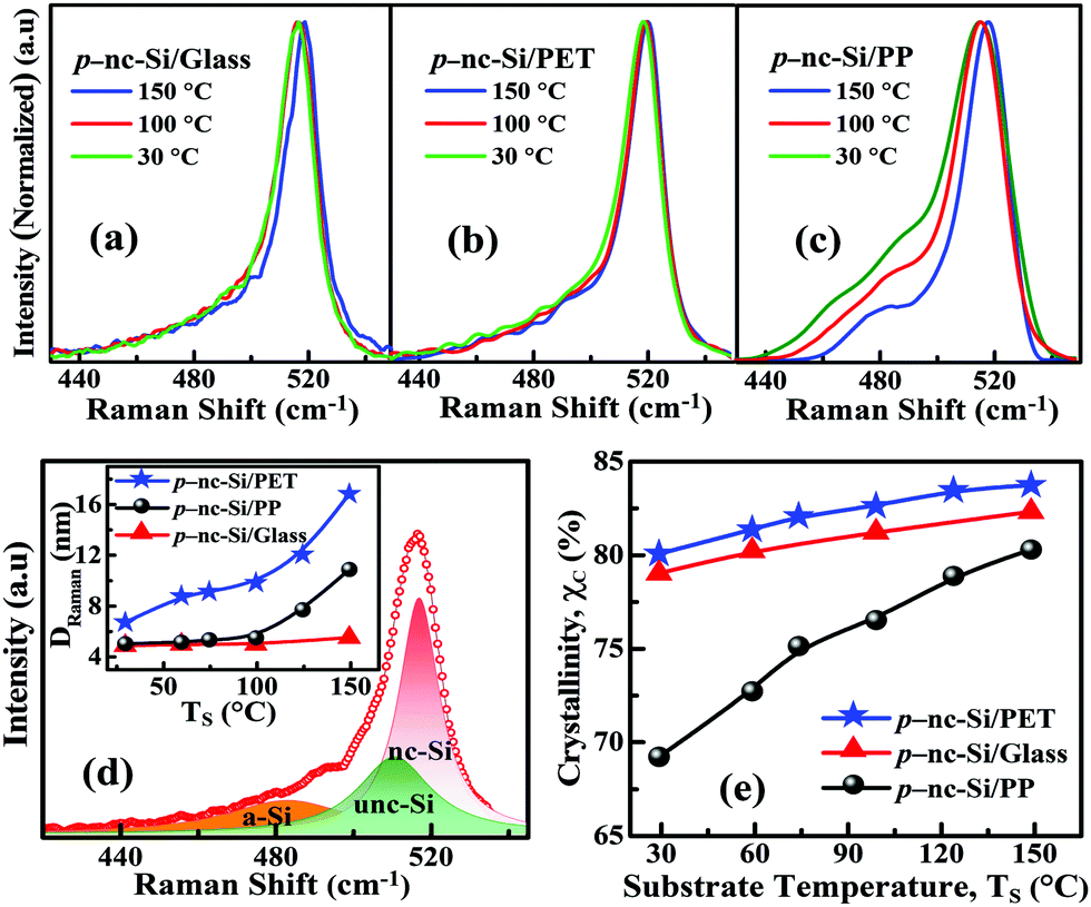 | ||
| Fig. 1 Raman spectra of p-nc-Si:H films grown at different substrate temperatures (TS) on (a) glass, (b) polyester film (PET) and (c) photo-plate (PP) substrates. (d) Typical deconvolution of Raman spectrum. Inset: Substrate-dependent variation of grain size (DRaman) with TS. (e) Variation in crystallinity (χC) on the different substrates with TS. | ||
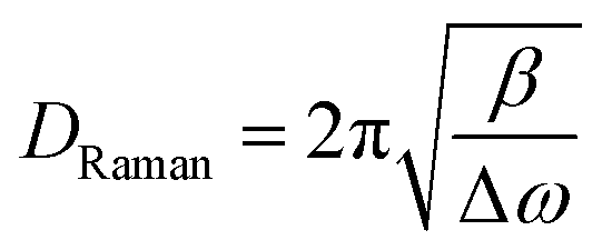
As plotted in Fig. 1(e), the network crystallinity (χC) of the B-doped nc-Si films on the PP substrate was found to be the lowest, which was only 80.2% at TS = 150 °C, and further reduced very fast at a lower TS, attaining ∼69.1% at TS = 30 °C, whereas it reduced only marginally in the other two cases. On the glass substrate, the crystallinity (χC) of the p-nc-Si films reduced from 82.2% to 78.9%, and interestingly, that on the PET substrates was marginally higher and reduced from ∼83.6% to only 80% with a decrease in TS from 150 °C to 30 °C. The nanocrystalline size (DRaman) was evaluated from the shift in nc-Si peak using the standard process23 as follows:
 | (2) |
The XRD spectra shown in Fig. 2(a) for the samples on glass substrates indicate the presence of the 〈111〉, 〈220〉 and 〈311〉 planes of c-Si, corresponding to the sharp peaks at 2θ ∼ 28.3°, 47.2° and 57.2°, respectively, demonstrating the good crystallinity of the network grown even at a low TS = 60 °C. For the PET substrate, the XRD peak at around 2θ ∼ 27° was so intense that the other two peaks at ∼47° and 55° were faint [Fig. 2(b)]. However, careful analysis via subtraction of the zoomed-in spectrum of the virgin substrate [Fig. 2(c)] from sample-on-substrate data [Fig. 2(d)] clearly identified, as shown in Fig. 2(e), the presence of a sharp 〈220〉 diffraction peak of Si nanocrystallites on the flexible PET substrate,28,29 which was generated via thermodynamically favoured growth.22,30 For the PP substrate, the sample signature could not been separated because of the very high intrinsic XRD response of the substrate itself. The average size (DXRD) of the nanocrystals corresponding to each crystallographic orientation was estimated from the FWHM (β) of the XRD peaks using the Scherrer equation23
DXRD = 0.9λ/βcos![[thin space (1/6-em)]](https://www.rsc.org/images/entities/char_2009.gif) θ θ | (3) |
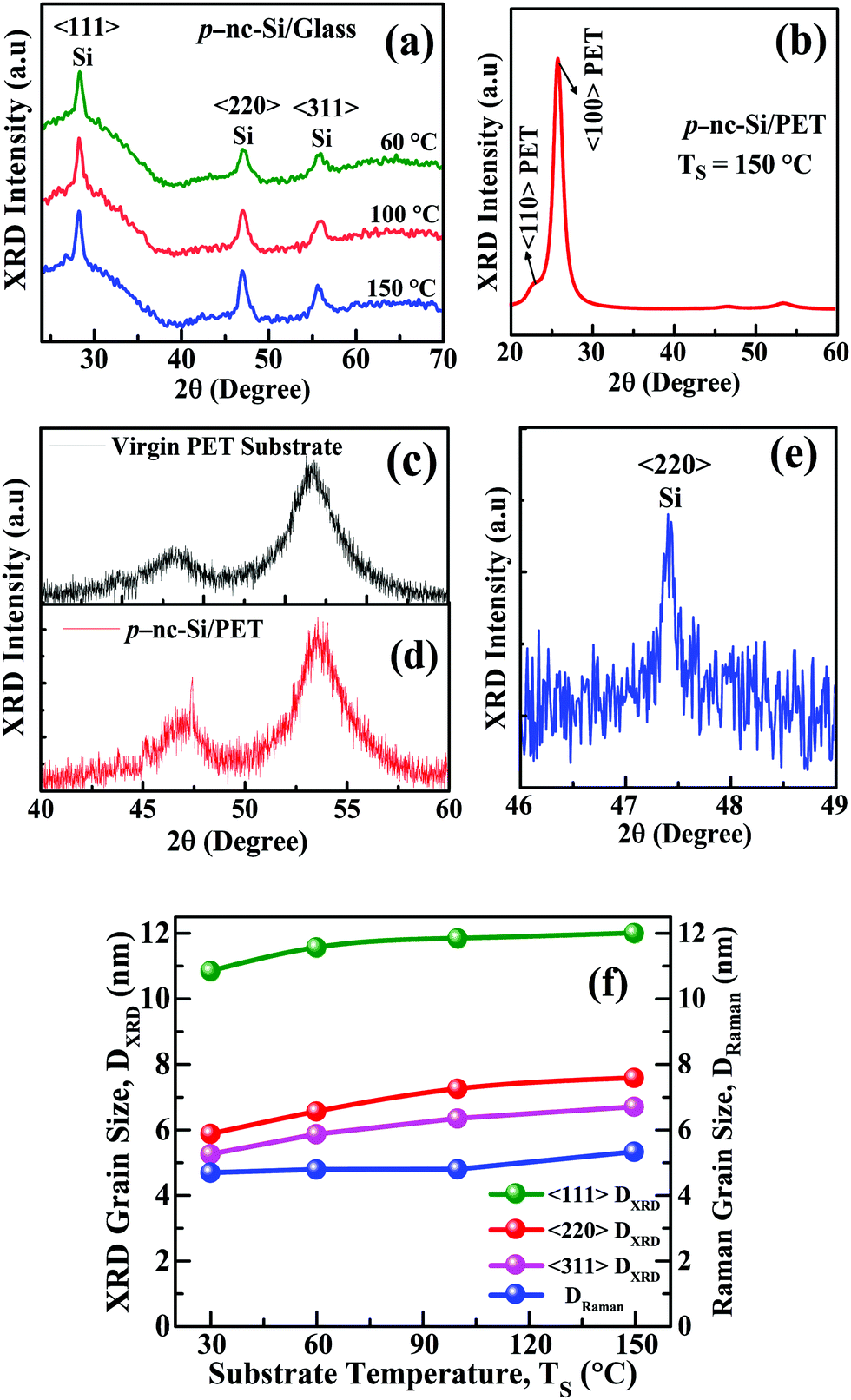 | ||
| Fig. 2 XRD spectra of p-nc-Si thin film on (a) glass and (b) PET substrate. Zoomed-in spectrum of (c) virgin PET substrate and (d) nc-Si film on PET substrate. (e) Intensity difference of XRD signal, identifying the presence of the 〈220〉 nc-Si peak as the sample response, removing the substrate effect. (f) Variation in the size (DXRD) of the nanocrystalline grains of different crystallographic orientations with TS and its comparison with that (DRaman) estimated from the Raman data for the p-nc-Si films deposited on glass substrates. | ||
In general, it was reported in earlier works32–35 that depending on the changes in different parameters when the grain size reduces, the crystalline volume fraction in the network deteriorates. However, it was also demonstrated for the Si-nc growth in the nc-Si/a-SiC and nc-Si/a-SiOx mixed phase network30,32,36 that despite the reduction in grain size, the crystallinity could improve via a rapid increase in the number of even smaller crystallites. In the present case, on gradually lowering the growth temperature, the crystalline volume fraction of the p-nc-Si network reduced systematically; however, the nature of the changes seemed to grossly vary depending on the characteristics of the substrate materials. In addition, comparing the data relating to the changes in crystalline volume fraction in Fig. 1(e) and the corresponding grain size in the inset in Fig. 1(d), it is apparent that the number density of crystallites are, in general, lower on the flexible photo-plate substrates than that on glass, which further reduced very quickly at TS < 75 °C, overall revealing the inferior crystallinity in the p-nc-Si network compared to that on the glass substrates. In contrast, superior crystallinity was attained in the p-nc-Si network grown on PET substrates by virtue of the larger size of the nanocrystallites together with their non-diminishing density with a decrease in the growth temperature.
The changes in the chemical structure of the films in terms of different Si–H bonding configurations and the amount of bonded H (CH) in the film network were investigated via infrared vibrational studies on the films deposited on p-type 〈111〉 c-Si substrates. Fig. 3(a) and (b) present the Si–H wagging and Si–H stretching vibration modes of the films prepared at different TS, together with their deconvolutions into various satellite components of Si–H wagging and rocking modes, their mono-, di- and tri-hydride stretching modes, and the Si–H–Si platelet-like configurations present in the matrix, respectively. The amounts of bonded H (CH) in the films were estimated using the following equation:37,38
 | (4) |
 corresponds to the integrated absorption by the Si–H wagging mode component at around 620 cm−1.
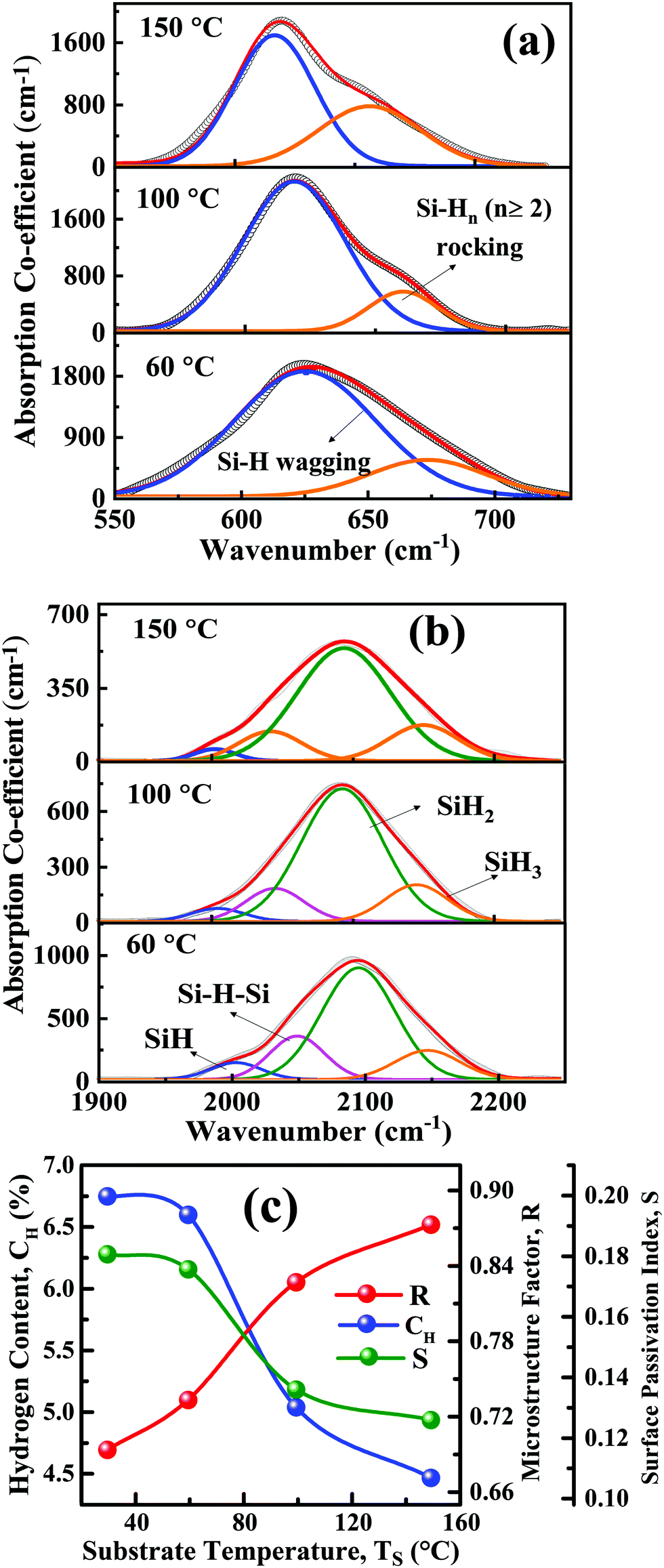 | ||
| Fig. 3 IR absorption spectra in (a) wagging mode vibration with Si–H wagging and Si–Hn (n ≥ 2) rocking components and (b) Si–H stretching mode vibration with different SiHn (n = 1, 2, and 3) components including Si–H–Si platelet-like component. (c) Variations in the bonded hydrogen content (CH), microstructure factor (R) and the surface passivation index (S) with growth temperature (TS) of the doped nc-Si films. | ||
Furthermore, according to the deconvoluted stretching mode absorption components, the microstructure factor (R), which is related to the poly-hydride fraction of the network,
| R = (ISiH3 + ISiH2)/(ISiH3 + ISiH2 + ISiH + ISi–H–Si) | (5) |
| S = ISi–H–Si/(ISiH3 + ISiH2 + ISiH + ISi–H–Si) | (6) |
The SEM images of the B-doped nc-Si films grown at the highest TS of ∼150 °C on the glass and PET substrates, as shown in Fig. 4(a) and (b), respectively, demonstrate that on glass the sample has a compact and granular structure with a homogeneous surface distribution of tiny and unique size grains with sharp grain boundaries. In contrast, on PET, the sample surface possesses an inhomogeneous morphology, comprised of a variety of larger-sized clusters (as identified by the areas enclosed by white borders) and irregular cracks with black lines of wide separations.40 In general, a larger average size (∼16.7 nm) of the grains on the PET substrate compared to that (∼5.3 nm) on the glass substrate was also determined using the Raman data [Fig. 1(d)]. However, for the sample grown on PET at 100 °C [Fig. 4(c)] its cluster size was smaller and its cracks were narrower.
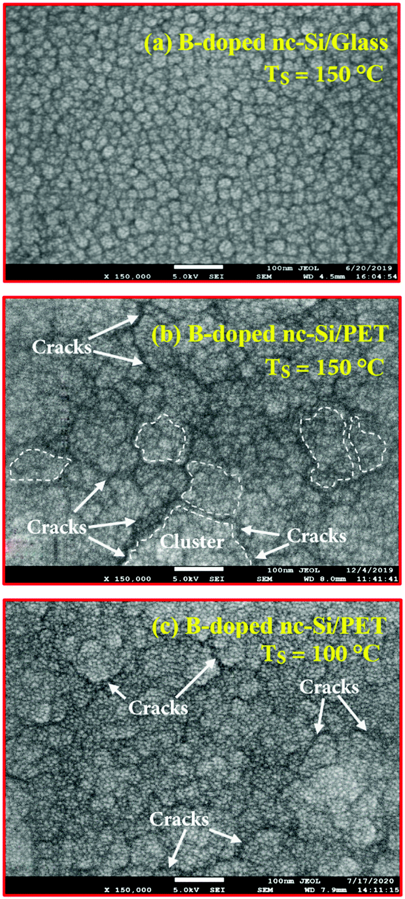 | ||
| Fig. 4 SEM images of p-nc-Si films on (a) glass, TS = 150 °C, and on PET substrate at (b) TS = 150 °C and (c) TS = 100 °C. | ||
The atomic force microscopy images of the B-doped nc-Si films grown on glass and PET substrates at different temperatures are shown in Fig. 5(a) and (b), respectively. For each type of substrate, the surface of the film deposited at a low temperature (30 °C) seemed to possess an inhomogeneous texture containing numerous voids, and consequently a relatively high surface roughness. The void density and the surface inhomogeneity sharply reduced at an elevated TS. Comparing the individual effects induced by the nature of the substrate and according to its consistently lower average surface roughness, as shown in Fig. 5(c), it seemed that the PET substrate facilitated better coalescence of the material, and hence an increase in overall crystallinity in the p-nc-Si network, as also evident from the Raman studies [Fig. 1(e)]. A similar observation was reported earlier41 in both AFM and Raman studies that second to the c-Si wafer substrate, the PET substrate propagates an improved crystalline network in the film than on glass substrate. However, with a further increase in TS ∼ 150 °C, the relatively higher surface roughness is consistent with the formation of surface cracks on the sample on the PET substrate, as evident from the SEM data in Fig. 4(b).
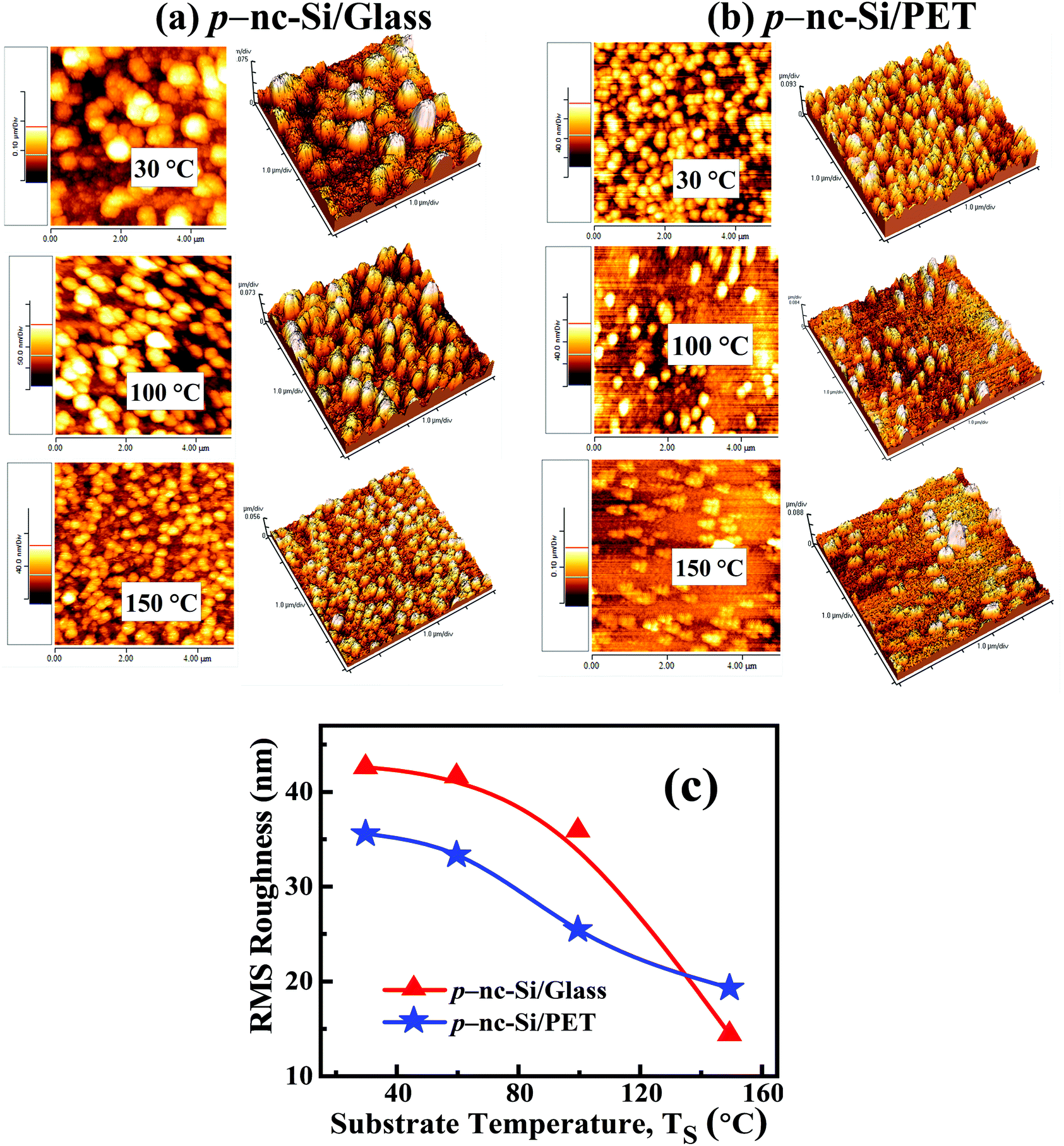 | ||
| Fig. 5 AFM images with 2D and 3D views of p-nc-Si films deposited on (a) glass and (b) PET substrates. (c) Comparison of the RMS roughness of the p-nc-Si films on glass and PET substrates at different TS. | ||
The TEM images of the samples prepared on C-coated Cu-microgrids at two different TS, ∼30 °C and 100 °C, are represented in Fig. 6(a) and (b), respectively. At the lowest TS of ∼30 °C, the TEM image reveals the dispersion of tiny crystallites within the amorphous network, as shown in Fig. 6(a-i). In the high-resolution image shown in Fig. 6(a-ii), individual nanocrystals containing distinctly separated lattice planes corresponding to the 〈111〉 and 〈220〉 crystal orientations are evident, which are further supported by the corresponding diffraction pattern in Fig. 6(a-iii). At a moderate TS of ∼100 °C, the TEM micrograph in Fig. 6(b-i) and the high-resolution image in Fig. 6(b-ii) reveal the prominent distribution of high density and comparatively large-size nanocrystallites dispersed in the amorphous matrix. The TED pattern in Fig. 6(b-iii) consists of very bright and sharp circular rings, wherein, in addition to the 〈111〉 and 〈220〉 planes, 〈311〉 nanocrystalline orientations can be distinctly observed, as also shown in Fig. 6(a-iii).23
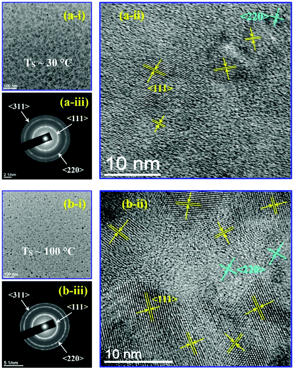 | ||
| Fig. 6 TEM images of p-nc-Si films grown at (a) TS of ∼30 °C and (b) 100 °C, in (i) moderate and (ii) high-resolution, and the corresponding (iii) SAED patterns. | ||
The optical properties of the B-doped nc-Si films grown on transparent rigid glass and flexible PET substrates were studied via UV-vis absorption. Fig. 7(a) represents the transmission spectra of the two films grown at 100 °C on two transparent substrates, glass and PET. Besides the mechanical measurement using a stylus, the film thickness was also optically assessed from the waves in the transmission spectra using the Swanepoel method.42 It is apparent from the spectral distribution that on the same run, the grown films were thicker on the glass than on PET. At TS = 100 °C, the B-doped nc-Si films grew on glass at a deposition rate of ∼14.9 nm min−1, while that on PET reduced to ∼7.5 nm min−1. The optical band gaps were estimated from the intercept of the linear slope of the Tauc plot (√αhν vs. hν) to α = 0 [Fig. 7(b)], following the standard process using the Tauc equation:43,44
| (αhν)1/2 = B(hν − Eg) | (7) |
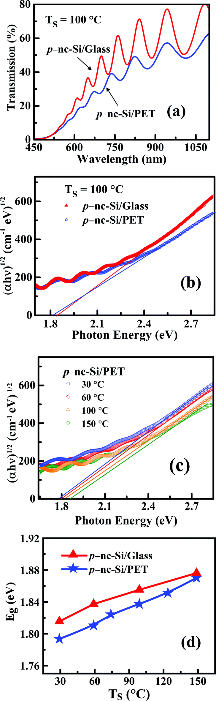 | ||
| Fig. 7 (a) Transmission spectra of p-nc-Si films grown on glass and PET substrates at TS = 100 °C and their (b) absorption data in the Tauc plot. (c) Comparison of the Tauc plots of the p-nc-Si films deposited at different TS on PET substrates and (d) comparison of the variations in Eg with TS for the samples on glass and PET substrates. | ||
The slope of the plots, i.e., the Tauc constant B, became very different for the p-nc-Si films deposited on the two different types of substrates in the same run, as shown in Fig. 7(b). The magnitude of B was higher in the case of the rigid glass substrate than that of the flexible PET substrate, and the optical band gaps (Eg) of the p-nc-Si films demonstrated higher magnitudes when deposited on glass. In general, the optical band gap of the B-doped nc-Si films reduced monotonically at a lower TS, as shown in Fig. 7(c), for the set of films grown on PET substrates. The slope of the plots, i.e., the Tauc constant B, remained very close, identifying a limited change in crystallinity within the range of variation in TS, 30–150 °C, wherein the crystalline volume fraction increased from 80% to 83.6% only, as estimated from the Raman data. Within the temperature range of 30–150 °C, the (Eg)Glass increased from 1.814 to 1.875 eV, while the relatively lower (Eg)PET = 1.792 eV at TS = 30 °C increased to ∼1.869 eV at TS = 150 °C, which was very close to that of the corresponding (Eg)Glass, as shown in Fig. 7(d).
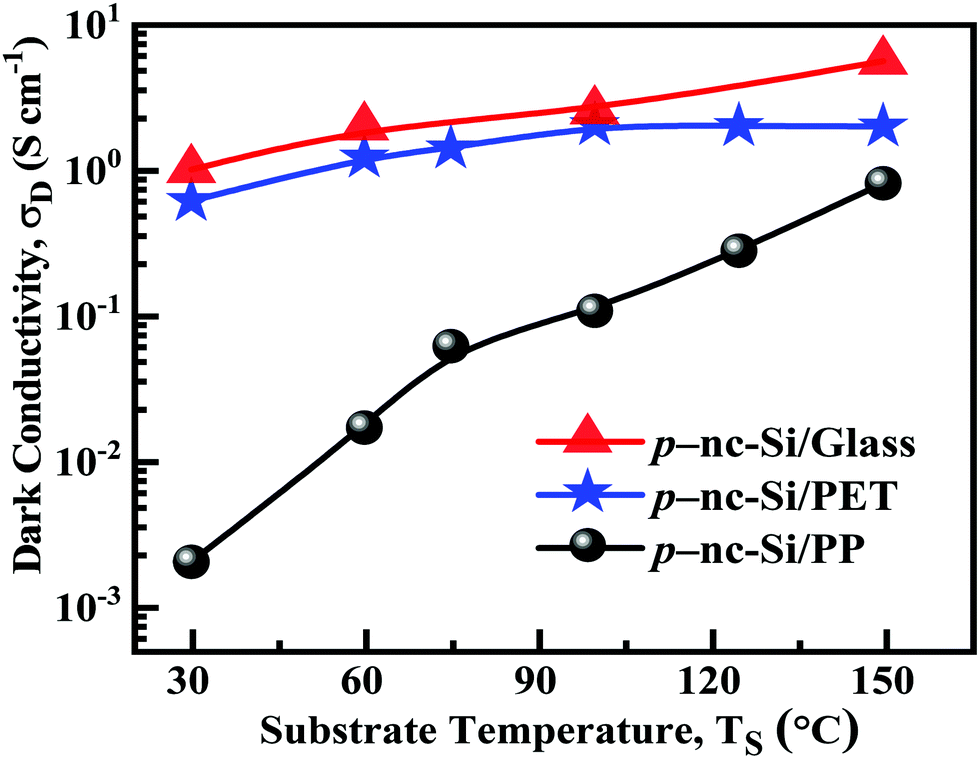
The plot of room temperature dark electrical-conductivity (σD) as a function of growth temperature (TS) in Fig. 8 indicates that (σD)Glass at each temperature had a trivially higher magnitude than (σD)PET, together with their similar nature of variation in the range of 30 ≤ TS (°C) ≤ 100, above which, the formation of significant surface cracks on the sample on PET may obstruct the regular TS-induced promotion of electrical transport, leading to a relatively larger difference in σD.45 Although (σD)PP at 150 °C was lower than the others, it further reduced by more than two orders of magnitude with a decrease in TS to 30 °C, with the deterioration being faster at TS below 75 °C. The B-doped nc-Si films having [(σD)PET]30°C ∼ 0.61 S cm−1 and [(σD)PET]100°C ∼ 2.02 S cm−1, with the corresponding [(Eg)PET]30°C ∼ 1.792 eV and [(Eg)PET]100°C ∼ 1.836 eV, and simultaneous crystallinity [(χC)PET]30°C ∼ 80% and [(χC)PET]100°C ∼ 82.5%, seem very attractive materials for application in solar cells with a tandem structure and flexible electronic devices using transparent PET substrates.
 | ||
| Fig. 8 Comparison of the TS-dependent σD of the p-nc-Si films grown on glass, photo-plate and PET substrates. | ||
Fig. 9(a) and (b) present the typical wide-scan XPS spectra of the B-doped nc-Si films grown on the flexible PET and rigid glass substrates, revealing distinct peaks of Si-2p and Si-2s at ∼100 eV and 150 eV, respectively, and a relatively weak peak at ∼187 eV, which corresponds to the B-1s component, representing its presence in a very small percentage as the dopant in the network.46 According to the B-1s peak, the individual contribution of the B-Si component was separated via spectral deconvolution, eliminating the impact of the plasmonic component, as shown in the insets in Fig. 9(a) and (b).23,47 The content of B in the doped nc-Si films was estimated from the ratio of integrated area under the B-Si peak with the combination of integrated areas under all the Si-peaks, e.g., Si-2p and Si-2s. Based on this analysis, the B concentration was estimated to be around 2.99, 3.25 and 3.45 at.% on the PET substrate, and 3.2, 3.55 and 3.95 at.% on the glass substrate for the samples prepared at TS = 30 °C, 100 °C and 150 °C, respectively, as presented in the bar chart shown in Fig. 9(c).
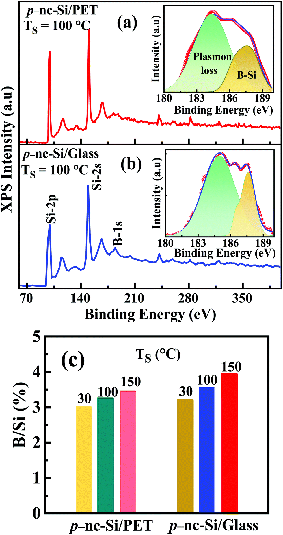 | ||
| Fig. 9 XPS data of p-nc-Si films on (a) PET and (b) glass substrates, and (c) estimated B to Si ratio in the doped nc-Si films grown on different substrates and at different TS presented in a bar chart. | ||
Discussion
In general, the photo-plate substrate provided less crystallinity for the nc-Si film, which may be attributed to the very different chemical nature and roughness of the substrate, which control the surface reactions.48 The emulsion layer containing silver halide grains dispersed in a gelatin matrix on the photo-plate substrate makes the surface rough, inhomogeneous and unstable, which encourage random growth. At elevated TS, the rapid removal of humidity from the gelatin-latex emulsion layer of the photo-plate surface causes the degree of crystallization, (χC)PP, to be closer to that of the other substrates, together with a similar elevation in (σD)PP. A significantly high (χC)Glass of ∼78.9% and remarkable (σD)Glass of ∼1 S cm−1 for the p-nc-Si film deposited at room temperature (TS = 30 °C) from SiH4 without additional H2 dilution are the result of the unique high electron density (∼1012 cm−3) plasma of ICP-CVD, which demonstrates a very special route for high yield nanocrystalline growth.24During nanocrystallization, the formation dynamics of the incubation layer at the substrate surface dominantly controls the subsequent growth kinetics, which in turn, sensitively depends on the substrate material and morphology, besides parameters such as temperature and electrical bias.22 Undoped poly-Si thin films grown on a PET substrate using SiH4 in 99.5% H2 dilution in conventional RF PE-CVD demonstrated the maximum conductivity ∼8.4 × 10⁻⁵ S cm−1, corresponding to the maximum crystallinity of ∼71.5% and narrowest optical band gap of ∼1.66 eV at a substrate bias of −100 V.40 At a very high −ve bias applied to the substrate, the band gap increased significantly due to nanocrystallization in the network, corresponding to a phase transition from high crystallinity towards an amorphous-dominated structure. Using extremely high H2 dilution in the SiH4 plasma in capacitively coupled RF PE-CVD, a crystalline volume fraction of up to 68.8% was previously reported49 for a B-doped nc-Si sample grown on PET substrate at −120 V bias, revealing the maximum magnitude of dark conductivity of ∼1.94 S cm−1. However, a further increase in bias caused high-energy H+ ion bombardment and subsequent degradation of the crystallinity. In the doped μc-Si:H films deposited at TS = 100 °C, a higher crystalline volume fraction (χC ∼ 68%) on the PET substrate compared to that on glass (only ∼22%) was reported by Dirani et al.,41 while 74% crystallinity was obtained on a single crystal Si substrate. However, their P-doped μc-Si:H films prepared from highly H2-diluted SiH4 plasma in RF-PECVD on a PET substrate demonstrated very low dark conductivity, σD, of ∼5 × 10⁻⁶ S cm−1, which was only 2 times higher than that on a glass substrate. In B-doped μc-Si films deposited by HW-CVD using 93.5% H2-diluted SiH4, Alpuim et al.50 obtained a similar increase in crystalline volume fraction for the samples deposited on PET substrates (χC ∼ 72%) compared to that on glass substrates (χC ∼ 65%), although the conductivity of the samples on PET (σD ∼ 2.6 × 10⁻¹ S cm−1) was lower than that on glass (σD ∼ 8.9 × 10⁻¹ S cm−1).
Because of similar reasons in facilitating device fabrication, besides Si in its different structural configurations, e.g., amorphous, nanocrystalline, microcrystalline and polycrystalline thin films, various other semiconductor thin films, e.g., CdS,51 ZnO,52,53 In-doped ZnO (IZO),54 Al-doped ZnO (AZO),55 were deposited simultaneously on flexible PET and rigid glass substrates and studied with their differences in opto-electronic properties. It was identified that, in general, these films possessed higher crystallinity; however, simultaneously narrower optical band gaps and mostly lower electrical conductivity when deposited on PET substrate than on glass substrate.
In the present investigation, the superior crystallinity on the flexible PET substrate originated from the strain-induced crystallization at the incubation layer due to substrate bending via plasma heating.56 The stress generated at the substrate/incubation layer interface provides the activation energy for nanocrystallization and favours the formation of larger nanocrystals at elevated TS and also leads to a gradually increased difference in crystallinity, although trivially, compared to that on glass substrate.57,58 Although possessing a higher (χC)PET (∼80%), the (σD)PET (∼6.01 × 10⁻¹ S cm−1) of the p-nc-Si film prepared at ambient temperature (TS = 30 °C) appeared to be slightly lower than (σD)Glass (∼9.95 × 10⁻¹ S cm−1) and this deviation increased at TS > 100 °C, which indicates that the surface strain/bending may not be favorable for electrical transport in samples on flexible PET substrates. This becomes more severe at higher TS due to the formation of micro-cracks on the sample surface. Although better network ordering corresponding to higher crystallinity resulted in a wider optical band gap (Eg) in the p-nc-Si films at elevated TS in the range of 30–150 °C on both the flexible PET and rigid glass substrates, fundamentally Eg always exhibit a lower magnitude in PET than on glass.
Generally, the optical band gap of the Si:H network depends on two major factors, the intrinsic network structure and the bonded H content (CH), including its nature of bonding as mono, di- or poly-hydride. In the case of an Si:H network with moderate crystallinity (containing a significant amount of amorphous component) and lower σD, normally with an increase in the deposition temperature, CH reduces and the SiHn bond becomes gradually less poly-hydride in configuration, which together lead to a systematic decrease in the optical band gap.59 By scavenging the H attached to the Si-network via atomic F and H together, on the ECR-CVD-grown Si:H films normally possessing a huge hydrogen content, relatively non-rigid network containing a significant amount of voids, and consequently a wide optical gap, it was demonstrated that the optical band gap changed proportionally with the bonded H content.60 Furthermore, in Si:H films possessing a low H content prepared by repeating growth interruption, and subsequently increasing the dose of H plasma treatment in both ECR-CVD and capacitively coupled PE-CVD, systematic widening of the optical band gap was obtained by virtue of the gradual increase in poly-hydrogenation of the network and significant network ordering, even with the simultaneous significant elimination of bonded H from the network.60–62 It was reported by Mahan el al.63 that the intrinsic optical band gap of the SiH network in medium range order, (Eg)MRO, follows the empirical relation: Eg = (Eg)MRO + 0.0135 CH, where Eg is the experimentally determined optical band gap and CH is the bonded H content of the network. Furthermore, they demonstrated that the magnitude of (Eg)MRO increases linearly with an increase in network ordering. In the case of the present series of B-doped nc-Si films deposited on glass and PET substrates, the amount of H bonded to the network is very low by virtue of the high crystallinity of the network and simultaneous unavailability of surplus atomic H in the plasma because of the use SiH4 plasma without deliberate H2 dilution in ICP-CVD. Within this network, the increase in the experimentally determined optical band gap (Eg) on removal of H and simultaneous increase in the microstructure factor (R) at an elevated growth temperature (TS) [Fig. 3(c)] essentially signify the systematic widening of the intrinsic optical band gap, (Eg)MRO or (Eg)SRO, due to the gradual temperature-mediated improvement in the network towards short-range ordering (SRO). This phenomenon applies equally for films grown on glass and flexible PET substrates, where a virtually identical linear elevation in the optical band gap has been revealed with an increase in the growth temperature-mediated network crystallinity (Fig. 10).
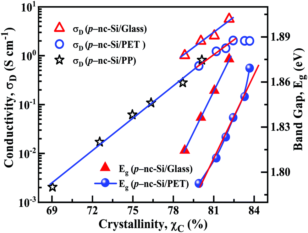 | ||
| Fig. 10 Variation in the room temperature electrical conductivity of p-nc-Si films on glass, PP and PET substrates, demonstrating excellent systematic changes arising from the modification of crystallinity occurring with an increase in the growth temperature. The optical band gap of the films grown on glass and PET substrates showing individual linear widening with an increase in TS. | ||
At TS = 150 °C, the deviation in (Eg)PET from linearity is consistent with the similar deviation of (σD)PET and indicates the restriction of the substrate temperature with the use of the PET substrate, arising from its specific chemical nature. Furthermore, the difference in the magnitude of the estimated Eg of the two samples grown in the same run on glass and PET substrates may arise due to the change in the transparency of the PET substrate, which is different in chemical nature from glass, via plasma exposure at the early stage of film growth and that remaining unaccounted for in the process considering the reference substrate during optical measurements, thereby revealing a relatively narrower optical band gap (Fig. 10).
The electrical conductivity of the B-doped nc-Si films was found to have a direct one-to-one correlation with the network crystallinity. Under the investigated conditions, the crystalline volume fraction in the network grown on both flexible substrates (PP and PET) from the SiH4 plasma undiluted by additional H2 in ICP-CVD, follows a single straight-line relation, as shown in Fig. 10. At very high crystallinity, χC > 82.5%, the p-nc-Si film deposited on PET at TS > 100 °C showed little deviation in the straight-line relation of σD, which may arise because of the formation of surface cracks on the sample, hindering the usual transport of charge carriers across the network. In addition, the improved σD of the films on the glass substrate may occur due to the higher carrier density by virtue of increased dopant activation (Fig. 8) as an individual effect arising from the particular chemical nature of the substrate;50 however, a similar linear relation with identical slope between χC and σD was maintained, as demonstrated in Fig. 10. The incorporation of an increased amount of dopant could result in increased distortion in the tiny host crystallites, and thereby, cause reduced crystallization in the network grown on the glass substrate than on PET substrate.
In the process of film growth by PECVD, the adsorption of the plasma precursors on the substrate, their temperature-mediated diffusion across the substrate surface, and finally sticking at some low energy site via the formation of chemical bonds with the substrate at an early stage are the different sequential steps involved. Therefore, in the elementary adsorption process, the chemical affinity between the substrate and the precursors plays a major role. The SiHn precursors easily form bonds with the similar Si element of the glass substrate via its abundant dangling bond, which results in a higher deposition rate compared to that on the PET substrate, where C is the major bonding element with various functional groups such as –COOH, –OH, and –C![[double bond, length as m-dash]](https://www.rsc.org/images/entities/char_e001.gif) O.64 During the subsequent process, the evolution of the substrate surface roughness and creation of voids at the interface between the substrate and the incubation area of the growth zone, which is initiated by inhomogeneous etching of the weak Si–Si bonds by atomic H of the plasma, result in structural reorientation and the formation of islands. These are the first set of nuclei, and nucleation becomes predominant for slower network formation during silicon nanocrystallization.65–67 In the early stage of growth of the nanocrystalline network, the deposition continues typically via the development of already existing nuclei because of the lower energy requirement, forming a columnar growth morphology.68,69 However, new nuclei are formed simultaneously, and the growth continues along the lateral dimension. Gradual coalescence of the columnar structures via lateral extension produces a compact and rigid network. Hence, the initial formation of nuclei controls the subsequent growth dynamics and determines the final network structure. This aspect highlights the importance of the substrate. The structural morphology and the chemical composition of the substrate, together with the growth parameters determine the nucleation, columnar configuration and amalgamation of the growth species. Thus, the better compliance via surface deformation on the flexible PET substrate compared to the rigid glass substrate affords intrinsic stress relaxation and promotes spontaneous crystallization in the Si network.
O.64 During the subsequent process, the evolution of the substrate surface roughness and creation of voids at the interface between the substrate and the incubation area of the growth zone, which is initiated by inhomogeneous etching of the weak Si–Si bonds by atomic H of the plasma, result in structural reorientation and the formation of islands. These are the first set of nuclei, and nucleation becomes predominant for slower network formation during silicon nanocrystallization.65–67 In the early stage of growth of the nanocrystalline network, the deposition continues typically via the development of already existing nuclei because of the lower energy requirement, forming a columnar growth morphology.68,69 However, new nuclei are formed simultaneously, and the growth continues along the lateral dimension. Gradual coalescence of the columnar structures via lateral extension produces a compact and rigid network. Hence, the initial formation of nuclei controls the subsequent growth dynamics and determines the final network structure. This aspect highlights the importance of the substrate. The structural morphology and the chemical composition of the substrate, together with the growth parameters determine the nucleation, columnar configuration and amalgamation of the growth species. Thus, the better compliance via surface deformation on the flexible PET substrate compared to the rigid glass substrate affords intrinsic stress relaxation and promotes spontaneous crystallization in the Si network.
Conclusion
It was assessed that compared to the rigid glass, better compliance by means of deformation of the flexible polyethylene terephthalate (PET) substrate provides plausible intrinsic stress relaxation during the evolution of the film network via energy transfer across the film-substrate interface, which facilitates improved network crystallinity within a sustainable temperature limit up to 100 °C. The inherent high electron density of the ICP-CVD provided surplus atomic H within the low pressure SiH4 plasma without additional H2 dilution and the favorable strain-induced nanocrystallization kinetics at the incubation layer, arising from surface bending via plasma heating of the flexible PET substrate, which together promoted the high yield advanced crystallinity even at ambient temperature. The B-doped nc-Si films on PET substrate possessed high electrical conductivity and wide optical band gap by virtue of its functional dopability and high crystallinity, and exhibited the overall optoelectronic properties similar to that on glass substrates. The superior crystallinity (χC ∼ 82.5%) with an average grain size, DRaman, of ∼9.63 nm, wide band-gap, Eg, of ∼1.836 eV and high electrical conductivity, σD, of ∼2.02 S cm−1 of the low-temperature (TS = 100 °C) deposited B-doped nc-Si film on transparent and flexible PET substrate seem ideal for the window layer in nc-Si solar cells in the p–i–n superstrate configuration and also very suitable for application in low-cost flexible electronics. For large-scale device fabrication involving process automation, flexible polyethylene substrates are uniquely suitable, and the present work identifies an essential low temperature (∼100 °C) avenue for the growth of device-grade p-nc-Si films via CMOS compatible plasma processing of SiH4 without deliberate H2 dilution using low-pressure, high-density, planar inductively coupled plasma.Author contributions
The authors declare that they have equal contributions in this publication.Conflicts of interest
The authors declare that they have no known competing financial interests or personal relationships that could have appeared to influence the work reported in this paper.Acknowledgements
The work has been done under Nano-Silicon projects funded by the Department of Science and Technology (Nano-Mission Program) and the Council of Scientific and Industrial Research, Govt. of India. One author (C. P.) acknowledges DST, GoI, for providing INSPIRE Fellowship.References
- K. Nomura, H. Ohta, A. Takagi, T. Kamiya, M. Hirano and H. Hosono, Room-temperature fabrication of transparent flexible thin-film transistors using amorphous oxide semiconductors, Nature, 2004, 432, 488–492 CrossRef CAS.
- J. G. Lee, Y. G. Seol and N. E. Lee, Polymer thin film transistor with electroplated source and drain electrodes on a flexible substrate, Thin Solid Films, 2006, 515, 805–809 CrossRef CAS.
- A. Pecora, L. Maiolo, M. Cuscunà, D. Simeone, A. Minotti, L. Mariucci and G. Fortunato, Low-temperature polysilicon thin film transistors on polyimide substrates for electronics on plastic, Solid State Electron., 2008, 52, 348–352 CrossRef CAS.
- G. Qin, H. C. Yuan, H. Yang, W. Zhou and Z. Ma, High-performance flexible thin-film transistor fabricated using print–transferrable polycrystalline silicon membranes on a plastic substrate, Semicond. Sci. Technol., 2011, 26, 025005–025010 CrossRef.
- P. Y. Hsieh, C. Y. Lee and N. H. Tai, A high carrier-mobility crystalline silicon film directly grown on polyimide using SiCl4/H2 microwave plasma for flexible thin film transistors, J. Mater. Chem. C, 2015, 3, 7513 RSC.
- N. Liu, K. N. Yun, H. Y. Yu, J. H. Shim and C. J. Lee, High-performance carbon nanotube thin-film transistors on flexible paper substrates, Appl. Phys. Lett., 2015, 106, 103106 CrossRef.
- S. M. Han, J. H. Park, S. G. Park, S. J. Kim and M. K. Han, Hydrogenation of nanocrystalline Si thin film transistors employing inductively coupled plasma chemical vapor deposition for flexible electronics, Thin Solid Films, 2007, 515, 7442–7445 CrossRef CAS.
- T. Sekitani, U. Zschieschang, H. Klauk and T. Someya, Flexible organic transistors and circuits with extreme bending stability, Nat. Mater., 2010, 9, 1015–1022 CrossRef CAS.
- X. Yu, L. Zeng, N. Zhou, P. Guo, F. Shi, D. B. Buchholz, Q. Ma, J. Yu, V. P. Dravid, R. P. H. Chang, M. Bedzyk, T. J. Marks and A. Facchetti, Ultra-flexible, “invisible” thin film transistors enabled by amorphous metal oxide/polymer channel layer blends, Adv. Mater., 2015, 27, 2390–2399 CrossRef CAS.
- A. Shah, P. Torres, R. Tscharner, N. Wyrsch and H. Keppner, Photovoltaic technology: the case for thin-film solar cells, Science, 1999, 285, 692–698 CrossRef CAS.
- F. Priolo, T. Gregorkiewicz, M. Galli and F. T. Krauss, Silicon nanostructures for photonics and photovoltaics, Nat. Nanotechnol., 2014, 9, 19–32 CrossRef CAS.
- H. Yamamoto, Y. Takaba, Y. Komatsu, M. J. Yang, T. Hayakawa, M. Shimizu and H. Takiguchi, High-efficiency μc-Si/c-Si heterojunction solar cells, Sol. Energy Mater. Sol. Cells, 2002, 74, 525–531 CrossRef CAS.
- K. Tao, D. Zhang, Y. Sun, L. Wang, J. Zhao, Y. Xue, Y. Jiang, H. Cai, Y. Sui and J. Wang, n–i–p, Proc. of 4th IEEE Int. Conf. on Nano/Micro Engineered and Molecular Systems, Shenzhen, China (2009), pp. 327–330.
- Z. Huang, L. R. Dahal, M. M. Junda, P. Aryal, S. Marsillac, R. W. Collins and N. J. Podraza, Characterization of structure and growth evolution for nc-Si:H in the tandem photovoltaic device configuration, IEEE J. Photovoltaics, 2015, 5, 1516–1522 Search PubMed.
- J. K. Rath and R. E. I. Schropp, Incorporation of p-type microcrystalline silicon films in amorphous silicon based solar cells in a superstrate structure, Sol. Energy Mater. Sol. Cells, 1998, 53, 189–203 CrossRef CAS.
- T. Söderström, F. J. Haug, V. Terrazzoni-Daudrix and C. Ballif, Optimization of amorphous silicon thin film solar cells for flexible photovoltaics, J. Appl. Phys., 2008, 103, 114509 CrossRef.
- L. Leopreknat, M. S. White, E. D. Głowacki, M. C. Scharber, T. Zillger, J. Rühling, A. Hübler and N. S. Sariciftci, 4% Efficient polymer solar cells on paper substrates, J. Phys. Chem. C, 2014, 118, 16813–16817 CrossRef.
- K. Wilken, F. Finger and V. Smirnov, Annealing effects in low temperature amorphous silicon flexible solar cells, Energy Procedia, 2015, 84, 17–24 CrossRef CAS.
- S. Sriraman, S. Agrawal, E. S. Aydil and D. Maroudas, Mechanism of hydrogen-induced crystallization of amorphous silicon, Nature, 2002, 418, 62 CrossRef CAS.
- D. Das and M. Jana, Hydrogen plasma induced microcrystallization in layer-by-layer growth scheme, Sol. Energy Mater. Sol. Cells, 2004, 81, 169–181 CrossRef CAS.
- M. Kondo, Y. Nasuno, H. Mase, T. Wada and A. Matsuda, Low-temperature fabrication of microcrystalline silicon and its application to solar cells, J. Non-Cryst. Solids, 2012, 299–302, 108–112 Search PubMed.
- D. Das, D. Raha, W. C. Chen, K. H. Chen, C. T. Wu and L. C. Chen, Effect of substrate bias on the promotion of nanocrystalline silicon growth from He-diluted SiH4 plasma at low temperature, J. Mater. Res., 2012, 27, 1303–1313 CrossRef CAS.
- C. Patra and D. Das, Electrically active boron doping in the core of Si nanocrystals by planar inductively coupled plasma CVD, J. Appl. Phys., 2019, 126, 155305 CrossRef.
- D. Kar and D. Das, Conducting wide band gap nc-Si/a-SiC:H films for window layers in nc-Si solar cells, J. Mater. Chem. A, 2013, 1, 14744–14753 RSC.
- C. Ossadnik, S. Veprek and I. Gregora, Applicability of Raman scattering for the characterization of nanocrystalline silicon, Thin Solid Films, 1999, 337, 148–151 CrossRef CAS.
- G. Zatryb, J. Misiewicz, P. R. J. Wilson, J. Wojcik, P. Mascher and A. Podhorodecki, Stress transition from compressive to tensile for silicon nanocrystals embedded in amorphous silica matrix, Thin Solid Films, 2014, 571, 18–22 CrossRef CAS.
- W. Wei, G. Xu, J. Wang and T. Wang, Raman spectra of intrinsic and doped hydrogenated nanocrystalline silicon films, Vacuum, 2007, 81, 656–662 CrossRef CAS.
- B. Hekmatshoar, D. Shahrjerdi, S. Mohajerzadeh, A. Khakifirooz, A. Goodarzi and M. Robertson, Low temperature crystallization of germanium on plastic by externally applied compressive stress, J. Vac. Sci. Technol., A, 2003, 21, 752 CrossRef CAS.
- S. Paydavosi, A. Ebrahimi, A. H. Tamaddon, S. Mohajerzadeh, N. Izadi, A. Behnam and M. D. Robertson, Hydrogenation assisted nickel-induced lateral nano-crystallization of amorphous silicon on flexible plastic substrates at low temperatures, Thin Solid Films, 2008, 516, 7790–7796 CrossRef CAS.
- D. Das and D. Kar, Self-assembled nc-Si-QD/a-SiC thin films from planar ICP-CVD plasma without H2-dilution: a combination of wide optical gap, high conductivity and preferred 〈220〉 crystallographic orientation, uniquely appropriate for nc-Si solar cells, RSC Adv., 2016, 6, 3860–3869 RSC.
- B. Sain and D. Das, Low temperature plasma processing of nc-Si/a-SiNx:H QD thin films with high carrier mobility and preferred (220) crystal orientation: a promising material for third generation solar cells, RSC Adv., 2014, 4, 36929–36939 RSC.
- H. K. Malik, S. Juneja and S. Kumar, Employing constant photocurrent method for the study of defects in silicon thin flms, J. Theor. Appl. Phys., 2019, 13, 107–113 CrossRef.
- D. Das and P. Mondal, Effect of oxygen on the optical, electrical and structural properties of mixed-phase boron doped nanocrystalline silicon oxide thin films, Appl. Surf. Sci., 2017, 423, 1161–1168 CrossRef CAS.
- Q. Cheng, S. Xu and K. Ostrikov, Rapid, low-temperature synthesis of nc-Si in high-density, non-equilibrium plasmas: enabling nanocrystallinity at very low hydrogen dilution, J. Mater. Chem., 2009, 19, 5134–5140 RSC.
- D. Das and B. Sain, Rapid synthesis of nc-Si/a-SiNx:H QD thin films by plasma processing for their cost effective applications in photonic and photovoltaic devices, RSC Adv., 2015, 5, 63572 RSC.
- D. Das and A. Samanta, Quantum size effects on the optical properties of nc-Si QDs embedded in an a-SiOx matrix synthesized by spontaneous plasma processing, Phys. Chem. Chem. Phys., 2015, 17, 5063 RSC.
- C. J. Fang, K. J. Gruntz, L. Ley, M. Cardona, F. J. Demond, G. Muller and S. Kalbitzer, The hydrogen content of a-Ge:H and a-Si:H as determined by IR spectroscopy gas evolution and nuclear reaction techniques, J. Non-Cryst. Solids, 1980, 35–36, 255–260 CrossRef CAS.
- S. Samanta and D. Das, Nanocrystalline silicon thin films from SiH4 plasma diluted by H2 and He in RF-PECVD, J. Phys. Chem. Solids, 2017, 105, 90–98 CrossRef CAS.
- A. Fontcuberta i Morral and P. Roca i Cabarrocas, Etching and hydrogen diffusion mechanisms during a hydrogen plasma treatment of silicon thin films, J. Non-Cryst. Solids, 2002, 299–302, 196–200 CrossRef CAS.
- J. Liu, Y. Zhang, Z. Fan, H. Sun and F. Shan, Low-temperature deposition of large-grain polycrystalline Si thin films on polyethylene terephthalate, Thin Solid Films, 2020, 707, 138065 CrossRef CAS.
- E. A. T. Dirani, A. M. Andrade, L. K. Noda, F. J. Fonseca and P. S. Santos, Effect of the substrate on the structural properties of low temperature microcrystalline silicon films – A Raman spectroscopy and atomic force microscopy investigation, J. Non-Cryst. Solids, 2000, 273, 307–313 CrossRef CAS.
- R. J. Swanepoel, Determination of the thickness and optical constants of amorphous silicon, J. Phys. E: Sci. Instrum., 1980, 16, 1214 CrossRef.
- J. Tauc, R. Grigorovici and A. Vancu, Optical properties and electronic structure of amorphous germanium, Phys. Status Solidi B, 1966, 15, 627 CrossRef CAS.
- B. Sain and D. Das, Development of nc-Si/a-SiNx:H thin films for photovoltaic and light-emitting applications, Sci. Adv. Mater., 2013, 5, 1–11 CrossRef.
- D. Das and B. Sain, Electrical transport phenomena prevailing in undoped nc-Si/a-SiNx:H thin films prepared by inductively coupled plasma chemical vapor deposition, J. Appl. Phys., 2013, 114, 073708 CrossRef.
- B. M. Monroy, G. Santana, J. Fandiño, A. Ortiz and J. C. Alonso, Growth of silicon nanoclusters on different substrates by plasma enhanced chemical vapor deposition, J. Nanosci. Nanotechnol., 2006, 6, 3752–3755 CrossRef CAS.
- C. Song, J. Xu, G. Chen, H. Sun, Y. Liu, W. Li, L. Xu, Z. Ma and K. Chen, High-conductive nanocrystalline silicon with phosphorous and boron doping, Appl. Surf. Sci., 2010, 257, 1337–1341 CrossRef CAS.
- M. Kondo, Y. Toyoshima, A. Matsuda and K. Ikuta, Substrate dependence of initial growth of microcrystalline silicon in plasma-enhanced chemical vapor deposition, J. Appl. Phys., 1996, 80, 6061 CrossRef CAS.
- D. Ma, J. Liu and W. Zhang, The effect of negative bias on the preparation conditions and structural changes in boron-doped nanocrystalline silicon thin films prepared on PET, J. Non. Cryst. Solids, 2017, 475, 53–58 CrossRef CAS.
- P. Alpuim, V. Chu and J. P. Conde, Doping of amorphous and microcrystalline silicon films deposited at low substrate temperatures by hot-wire chemical vapor deposition, J. Vac. Sci. Technol., A, 2001, 19, 2328 CrossRef CAS.
- J. H. Lee, Influence of substrates on the structural and optical properties of chemically deposited CdS films, Thin Solid Films, 2007, 515, 6089–6093 CrossRef CAS.
- M. G. Faraj, K. Ibrahim, M. H. Eisa, M. K. M. Pakhuruddin and M. Z. Pakhuruddin, Comparison of zinc oxide thin films deposited on the glass and polyethylene terephthalate substrates by thermal evaporation technique for applications in solar cells, Optoelectron. Adv. Mater., Rapid Commun., 2010, 4, 1587–1590 CAS.
- A. N. Banerjee, C. K. Ghosh, K. K. Chattopadhyay, H. Minoura, A. K. Sarkar, A. Akiba, A. Kamiya and T. Endo, Low-temperature deposition of ZnO thin films on PET and glass substrates by DC-sputtering technique, Thin Solid Films, 2006, 496, 112–116 CrossRef CAS.
- R. Mohammadigharehbagh, S. Pat, S. Özen, H. H. Yudar and S. Korkmaz, Investigation of the optical properties of the indium-doped ZnO thin films deposited by a thermionic vacuum arc, Optik, 2018, 157, 667–674 CrossRef CAS.
- H. L. Shen, H. Zhang, L. F. Lu, F. Jiang and C. Yang, Preparation and properties of AZO thin films on different substrates, Prog. Nat. Sci.: Mater. Int., 2010, 20, 44–48 CrossRef.
- M. P. Manoharan, S. Kumar, M. A. Haque, R. Rajagopalan and H. C. Foley, Room temperature amorphous to nanocrystalline transformation in ultra-thin films under tensile stress: an in situ TEM study, Nanotechnology, 2010, 21, 505707 CrossRef.
- B. J. Lee, C. S. Lee and J. C. Lee, Stress induced crystallization of amorphous materials and mechanical properties of nanocrystalline materials: a molecular dynamics simulation study, Acta Mater., 2003, 51, 6233–6240 CrossRef CAS.
- B. Hekmatshoar, S. Mohajerzadeh and D. Shahrjerdi, Thin-film tunneling transistors on flexible plastic substrates based on stress-assisted lateral growth of polycrystalline germanium, Appl. Phys. Lett., 2004, 85, 1054 CrossRef CAS.
- K. Bhattacharya and D. Das, Effect of deposition temperature on the growth of nanocrystalline silicon network from helium diluted silane plasma, J. Phys. D: Appl. Phys., 2008, 41, 155420 CrossRef.
- D. Das, Rigid amorphous silicon network from hydrogenated and fluorinated precursors in ECR-CVD, Sol. Energy Mater. Sol. Cells, 2004, 81, 155–168 CrossRef CAS.
- D. Das, Wide band gap Si:H at low H-content prepared by interrupted growth and H-plasma treatment, Jpn. J. Appl. Phys., 1994, 33, L571–L574 CrossRef CAS.
- D. Das, A novel approach towards silicon nanotechnology, J. Phys. D: Appl. Phys., 2003, 36, 2335–2346 CrossRef CAS.
- A. H. Mahan, R. Biswas, L. M. Gedvilas, D. L. Williamson and B. C. Pan, On the influence of short and medium range order on the material band gap in hydrogenated amorphous silicon, J. Appl. Phys., 2004, 96, 3818–3826 CrossRef CAS.
- L. Kinner, M. Bauch, R. A. Wibowo, G. Ligorio, E. J. W. List-Kratochvil and T. Dimopoulos, Polymer interlayers on flexible PET substrates enabling ultra-high performance, ITO-free dielectric/metal/dielectric transparent electrode, Mater. Des., 2019, 168, 107663 CrossRef CAS.
- D. Das, Plasma kinetics, surface phenomena and growth mechanism in hydrogenated amorphous silicon: Transition from amorphous to micro- and nano-crystalline Si:H, in Solid State Phenomena (Special Volume on Hydrogenated Amorphous Silicon), Scitec Publication, Switzerland, 1995, vol. 44–46, pp. 227–258 Search PubMed.
- P. Roca i Cabarrocas, N. Layadi, B. Drevillon and I. Solomon, Microcrystalline silicon growth by the layer-by-layer technique: long term evolution and nucleation mechanisms, J. Non-Cryst. Solids, 1996, 198–200, 871–874 CrossRef CAS.
- D. Raha and D. Das, Hydrogen induced promotion of nanocrystallization from He-diluted SiH4 plasma, J. Phys. D: Appl. Phys., 2008, 41, 085303 CrossRef.
- H. Shirai, B. Drevillon and I. Shimizu, Role of hydrogen plasma during growth of hydrogenated microcrystalline silicon: in situ UV-visible and infrared ellipsometry study, Jpn. J. Appl. Phys., 1994, 33, 5590 CrossRef CAS.
- M. Jana, D. Das, S. T. Kshirsagar and A. K. Barua, Control of crystallization at low thickness in μc-Si:H films using layer-by-layer growth scheme, Jpn. J. Appl. Phys., 1999, 38, L1087–L1090 CrossRef CAS.
| This journal is © The Royal Society of Chemistry 2021 |