
 Open Access Article
 This Open Access Article is licensed under a Creative Commons Attribution-Non Commercial 3.0 Unported Licence
Fluorinated porous silicon as sensor material for environmentally toxic gases: a first-principles study
José Eduardo
Santana
a,
Francisco
de Santiago
 a,
Álvaro
Miranda
*a,
Luis Antonio
Pérez
b,
Fernando
Salazar
a,
Alejandro
Trejo
a and
Miguel
Cruz-Irisson
a
a,
Álvaro
Miranda
*a,
Luis Antonio
Pérez
b,
Fernando
Salazar
a,
Alejandro
Trejo
a and
Miguel
Cruz-Irisson
a
aInstituto Politécnico Nacional, ESIME-Culhuacán, Av. Santa Ana 1000, 04430, Ciudad de México, Mexico. E-mail: amirandad.ipn@gmail.com
bInstituto de Física, Universidad Nacional Autónoma de México, C.P. 04510, Ciudad de México, Mexico
First published on 19th January 2021
Abstract
By using Density Functional Theory, the effect of adsorbed gas molecules on the electronic properties of fluorine passivated porous silicon (pSi) is investigated. A silicon nanopore is created by removing columns of atoms along the [001] crystallographic axis from a supercell of the bulk Si crystal. The Si dangling bonds of the generated pore are saturated with fluorine atoms except for the sites where gas molecules of NO, NO2 and SO2 are adsorbed. The adsorption energies, electronic densities of states and band structures of the different complexes formed by the nanopore and the adsorbed molecules are calculated and compared with previously reported results obtained for hydrogen-passivated pSi. The energy band gaps of the pSi-molecule complexes depend on the adsorbed species, opening the possibility of gas molecule recognition. The molecule adsorption energy is stronger for NO2. The understanding of molecule adsorption on silicon nanopores could lead to the development of novel sensing devices of environmentally hazardous gases.
Introduction
According to the Health Effects Institute (HEI), 90% of people around the world are breathing polluted air containing toxic gas molecules such as NOx and SOx, which causes around 6.1 million premature deaths per year.1 Also, the presence of these gases causes the ozone layer destruction (contributing to the greenhouse effect), acid rain, and the acidification of rivers and lakes.2,3 Therefore, the control of air pollution requires the study, design, and fabrication of devices and materials capable of detecting those polluting agents.During decades, materials such as electronic ceramics, metal oxides, semiconductors and conducting polymers have been studied to address their potential as toxic gas detectors,4–6 Particularly, bulk and nanoribbons of α-MoO3 and porous silicon oxycarbide have high sensitivity for the detection of harmful gases such as NO2.7–9 Moreover, nanostructured materials, such as silicene nanoribbons10 and graphene,11–13 have been proposed as potential detectors of other toxic gases, for example SO2, NH3 and CO. Silicon nanostructures, such as nanoporous structures and nanowires, have also gotten positive results in this task.14–16 Since its report of fabrication in 1990 by anodization in hydrofluoric acid (HF) of crystalline silicon substrates,17–19 porous silicon has generated great interest in the scientific community. Fast preparation, tuneable optical and electronic properties, large inner surface area, surface reactivity, good stability and full compatibility with modern electronic technology are some of the advantageous properties of pSi. In particular, a large surface area is required for a good molecule adsorption and pSi etched on p-type Si(100) provides a surface area of ∼200 m2 cm−3 and a site density of 6.8 × 10¹⁴ sites per cm2.20–22 Additionally, it has been proven that pSi can operate in a voltage range of 1–10 mV with a sensitivity range of 10–100 ppm.23 This allows the use of pSi in sensing electronic devices, ranging from the detection of several chemical agents to the identification of DNA chains and proteins.15,24–26 Moreover, several experimental studies have been done to prove that pSi, grown in [100] Si wafers, can be an active gas sensing device.5,27–30
In a similar way, surface chemistry has been proved to modify the electronic structures and optical behaviour of semiconductors.31 Hydrogen passivation causes a transition from metallic to semiconducting behaviour in Si nanowires32,33 and band gap changes in another Si nanostructures.34–37 Previous studies show that single-bonded atoms on Si surfaces, for example, Cl and F, may lightly diminish the energy bandgap.38–40 The same occurs with double-bonded atoms, such as N and O, but the bandgap decrement is larger in comparison with single-bonded atoms.41,42 However, it has been experimentally observed that the H-passivated pSi surface is rapidly oxidized in air,43,44 which leads the surface to irreversible modification and, consequently, a decrease in the sensitivity of this material to molecules such as NO2.45 Therefore, the surface fluorination of pSi is a key ingredient in this work, considering that the presence of fluorine atoms on the Si surface could inhibit the formation of silicon oxide46 and make the dissociation of adsorbed oxygen-containing molecules less likely. Even though the interactions between silicon surfaces and fluorine-containing molecules are complicated, the fluorination process of Si surfaces has been extensively studied. Wu and Carter report that F atoms only saturate the Si-dandling bonds.47 Also, Hoshino and Nishioka indicate that the development of F-passivated silicon surfaces is possible after a chemical reaction of hydrogen fluoride (HF) with H-passivated silicon surfaces.48,49 Otherwise, the fluorination of H-passivated silicon surfaces has been recently studied using different F-containing molecules.50 Fluorine-passivation is a feasible and advantageous way of tuning the electronic properties of pSi.
In a previous work, the adsorption of hazardous gas molecules, such as CO, NO, NO2 and SO2, on pSi passivated with hydrogen (pSi+H) was studied.15 Concerning to the fluorine-passivated pSi (pSi+F), there is not, to the best of our knowledge, a theoretical investigation of the adsorption properties of this passivation. For this reason, in this work, we study the effects of fluorine surface passivation of pSi on the adsorption of hazardous gas molecules such as NO2, SO2, and NO, and compare these results with those previously reported for pSi+H. To this end, the electronic band structures and energetic stabilities of the formed molecule-nanopore complexes, together with the molecule adsorption energies, charge excesses and desorption times, are analyzed. The results obtained are related to the potential application of pSi+F as chemical sensors.
Computational details and model
Density-Functional-Theory (DFT)51,52 calculations were carried out using the Perdew–Burke–Ernzerhof (PBE) exchange–correlation functional within the generalized-gradient approximation (GGA),53 with double-ζ polarized basis sets54,55 and norm-conserving Troullier–Martins pseudopotentials56 in their fully non-local form57 as implemented in the SIESTA code.58 For numerical integrations, a real-space grid defined by an energy cutoff of 160 Ry was considered. Geometry optimization was done through a conjugate gradient algorithm until the Hellmann–Feynman forces were less than 0.04 eV Å−1, with an average maximum value of 0.037 eV Å−1. The average energy change per atom was 2.79 × 10⁻⁶ eV, the maximum atomic displacement allowed in the optimization process was 0.105 Å, and the maximum and minimum obtained values for the atomic displacements were 2.52 × 10⁻³ Å and 9.56 × 10⁻⁵ Å, for pSi+H, respectively. Likewise, for pSi+F, the corresponding values were 2.08 × 10⁻³ Å and 4.37 × 10⁻⁵ Å.Following the Monkhorst–Pack scheme, the first Brillouin zone of the studied systems was sampled with a grid of 2 × 2 × 2 k-points.59 The Voronoi electronic population analysis was used to obtain the electronic charge transfer between gas molecules and the passivated pSi.60
A porous silicon supercell with 38.28% porosity is obtained by removing a column of atoms along the [001] direction of a bulk Si supercell, leading to {110} internal pore surfaces. The bulk crystalline Si supercell is formed by 4 × 4 × 4 cubic unit cells (8 atoms per unit cell). The resulting porous supercell, with periodic boundary conditions along the three spatial directions, has cell parameters a = b = c = 22.09 Å.
The dangling bonds of the exposed surfaces were saturated with fluorine atoms before the structural optimization was carried out, to prevent their reconstruction.
After the structural optimization of the fully passivated nanopores, one passivating atom was detached from a {110} facet to generate a Si dangling bond, and then this structure was structurally relaxed again. Fig. 1 shows the optimized passivated pSi structures together with the equilibrium configurations of the adsorbed molecules (NO, NO2 and SO2). The dangling bond sites (black arrows on Fig. 1) were used as adsorption sites for the molecules. For comparison purposes the same process was performed with H passivation, considering, as stated before, that the potential adsorption of these molecules would eventually lead to an oxidation of the pSi surface and a loss of sensing capabilities.
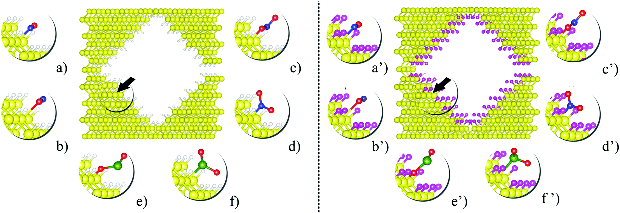 | ||
| Fig. 1 Optimized structures of pSi with H- (left panel) and F-passivation (right panel); together with the equilibrium configurations of (a and a′) NO(N), (b and b′) NO(O), (c and c′) NO2(O), (d and d′) NO2(N), (e and e′) SO2(S), (f and f′) and SO2(O) adsorbed molecules. The symbol in parenthesis indicates which atom of the adsorbed molecule is bonded to the pSi dangling bond. Yellow, white, magenta, green, blue and red spheres represent Si, H, F, S, N and O atoms, respectively. | ||
Results and discussion
In this section, we analyse the electronic band structure of F-passivated pSi, the HOMO–LUMO gap, the charge transfer from the molecule to the pSi, the molecule adsorption energy, the desorption time and the bond distance between the molecule and pSi.Hydrogen- and fluorine-passivated porous silicon
Fig. 2 and 3 show the charge density difference (CCD), the electronic band structure and PDOS of the structurally relaxed pSi+H and pSi+F, respectively.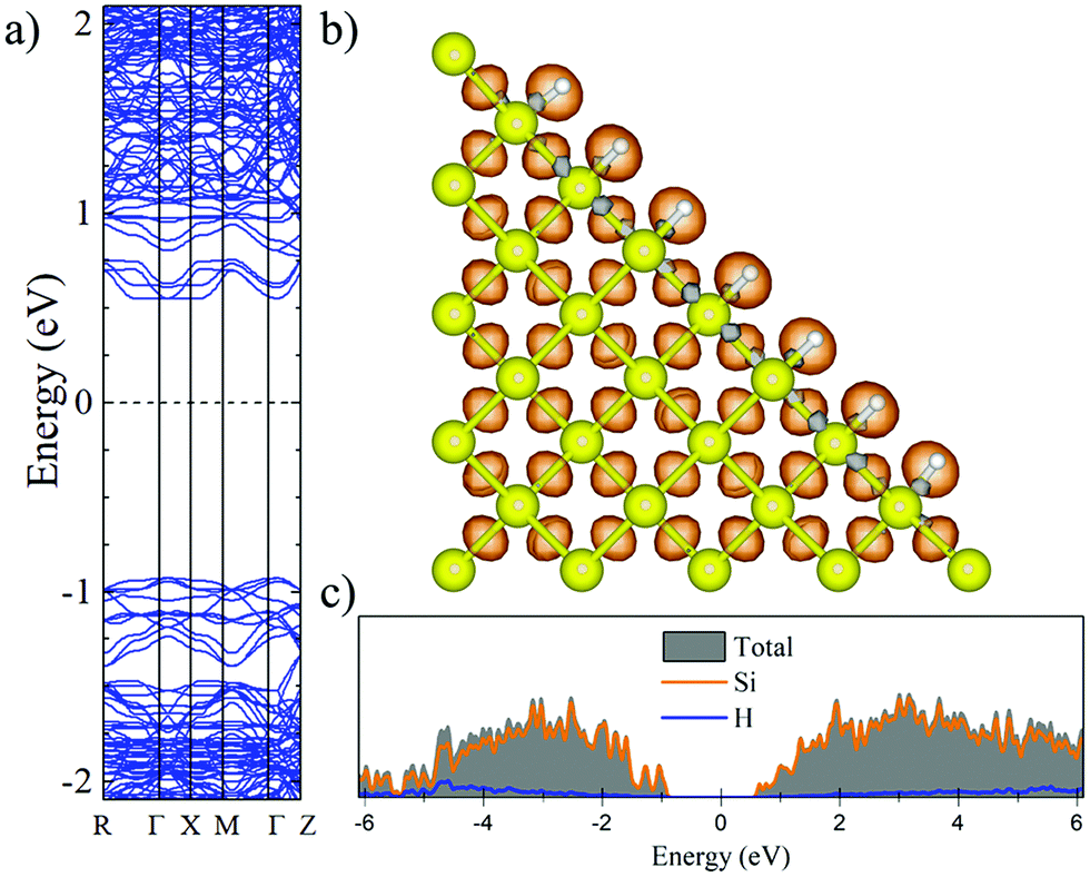 | ||
| Fig. 2 Electronic band structure (a), charge density difference (b) and PDOS (c) of the totally hydrogenated pSi after geometrical optimization. Orange (gray) isosurfaces denote gain (loss) of electronic charge in comparison with the ground-state charge density of the isolated atoms, for H-passivated pSi. | ||
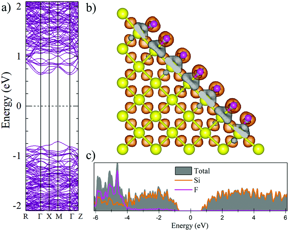 | ||
| Fig. 3 Electronic band structure (a), charge density difference (b) and partial electronic densities of states (c) of the fluorinated pSi after geometrical optimization. Orange (gray) isosurfaces denote gain (loss) of electronic charge in comparison with the ground-state charge density of the isolated atoms, for F-passivated pSi. | ||
The orange (gray) isosurfaces in Fig. 2b and 3b illustrate the gain (loss) of electronic charge in comparison with the ground-state charge density of the isolated atoms, for the pSi systems. They are given by:
δρ(![[r with combining right harpoon above (vector)]](https://www.rsc.org/images/entities/i_char_0072_20d1.gif) ) = ρX() − ρM(), ) = ρX() − ρM(), | (1) |
The Voronoi charge transfer from passivating atoms to Si atoms is markedly different between the F and H cases, having values of −0.1126 |e| and −0.0435 |e|, respectively. In case of F-passivation (Fig. 3b), we find a prominent redistribution of charge around the F atoms and on the Si surface (gray isosurface) in comparison with the H-passivated system (Fig. 2b). Also, we can see a decrement in the bandgap energy from 1.48 eV for H-passivation to 1.34 eV for F-passivation (Fig. 2a and 3a). This difference can be better understood with the partial density of species (PDOS) representation shown in Fig. 2c and 3c. The bonding energy between a surface Si and an H atom is 4.6 eV, indicating that the Si–H bonds are stable.61 The difference in electronegativities between H (2.2) and Si (1.9), indicates that this is a polar covalent bond, which is corroborated by both the charge excess on the H atoms and the charge density isosurfaces, where the higher charge density values are predominantly found close to the H atoms. There are small grey lobes around the Si surface atoms, which indicates that part of its charge gets transferred to the H as expected. Comparatively the F has similar characteristics, however, due to the much higher electronegativity of F, the bond became almost ionic in nature, and the surface silicon atoms undergo a greater charge loss, thus reflected in a narrower band gap due to the increase of available states of the surface Si atoms.
Adsorption and desorption properties
Fig. 4 shows the adsorption energy (EA) and the bond distance (β) between the molecules and the passivated pSi. For each molecule, we consider that bonding with pSi may be possible through each of their constituent elements, for example, in the case of NO2, we consider the cases in which N–Si or O–Si bonds may be created. The adsorption energy (EA) of a molecule adsorbed on the pSi is given by:14| EA = EMol + EX+DB − EX+DB+Mol + EBSSE, | (2) |
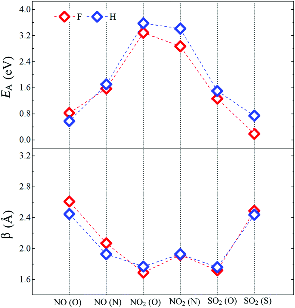 | ||
| Fig. 4 Adsorption energies (EA) and bond distances (β) between molecules and pSi for both kinds of passivation. Red and blue symbols represent pSi+F and pSi+H, respectively. | ||
After comparing the results of the adsorption energies and bond distances, it can be seen that the numerical results for H and F passivation follow each other very closely, indicating that the chemical composition on the superficial layer does not affect in a significant way the adsorption strength of the molecules. The larger EA among all the studied cases corresponds to the NO2 molecule. For H- and F-passivation schemes, these energies are 3.58 eV and 3.29 eV, respectively, when the bonding occurs through the O atom; and 3.41 and 2.87 eV, respectively, when the N atom is bonded to the pSi surface. Also, this molecule has the smallest bond distance between its O atom and the Si surface atom, being 1.77 Å for H-passivation and 1.69 Å for F-passivation; which is close to reported experimental Si–O bond length of 1.63 Å.63,64 For the Si–N bond, we found almost the same distance for pSi+H and pSi+F, being 1.93 and 1.92 Å, respectively. These distances are shorter than those found for Si–N bonds of 2.27 Å.65 On the other hand, the lowest EA corresponds to the NO (O) molecule on the pSi+H and the SO2 (S) molecule on the pSi+F, with EA of 0.58 eV and 0.19 eV, and bond distances of 2.45 and 2.49 Å, respectively. These results seem to indicate that the NO2 and SO2 molecules, when interacting through their O atoms, having the strongest binding energy, have a strong chemical interaction with the surface of the H- or F-passivated pSi.
For a NO molecule adsorbed on pSi with H (F) passivation, the corresponding adsorption energies are 0.58 eV (0.83 eV) and 1.71 eV (1.57 eV) when the bonding occurs through O and N, respectively. The NO-pSi distances are 2.45 Å (2.61 Å) when the bonding occurs through O, and 1.93 Å (2.07 Å) when the bonding occurs through N, exceeding the experimental reported results in both cases. For the H-passivated case, the adsorption energy of SO2 (S) (0.74 eV) is larger than that of the F-passivated case, but they have a similar bond distance of 2.44 Å. For SO2 (O), the adsorption energies and the bond distances are 1.50 eV, 1.26 eV and 1.76 Å, 1.72 Å, for the H- and F-passivated pSi, respectively. These results show that the NO2 has a tendency to get tightly bonded to the pSi surface, which hints that pSi may not be suitable for its detection since the adsorption of NO2 could lead to a fundamental change on the surface chemistry of the pSi which may not be able to be reversed.
For a better understanding, the adsorption reaction could be described as pSi(n−1) + X → pSi(n−1)X, where pSi refers to pSi+H or pSi+F, n is the maximum number of F or H surface passivating atoms on the pSi surface and (n − 1) denotes the existence of at least one dandling bond formed during the pSi synthesis. X refers to the adsorbed molecule (X = NO, NO2 or SO2) which can be adsorbed through both of its constituent atoms.
The van't Hoff–Arrhenius expression66,67 and the transition state theory give us the possibility to evaluate the recovery time of pSi+F and pSi+H after the molecule adsorption using the following equation:68,69
 | (3) |
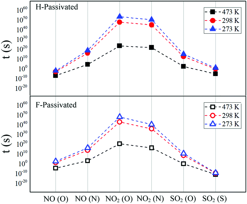 | ||
| Fig. 5 Desorption times (t) of molecules from pSi+H (top panel, solid symbols) and pSi+F (bottom panel, open symbols). Triangle, circles and square symbols represent the different tested temperatures: 273, 298, and 473 K, respectively. | ||
| Test temperature | ||||||
|---|---|---|---|---|---|---|
| 273 K | 298 K | 473 K | ||||
| pSi+H | pSi+F | pSi+H | pSi+F | pSi+H | pSi+F | |
| NO (O) | 2.22 × 10² | 5.70 × 10⁻³ | 1.15 × 101 | 7.14 × 10⁻⁴ | 2.59 × 10⁻⁵ | 7.88 × 10⁻⁸ |
| NO (N) | 1.17 × 10¹⁶ | 3.84 × 10¹⁸ | 4.27 × 10¹³ | 8.61 × 10¹⁵ | 8.62 × 10² | 2.06 × 10⁴ |
| NO2 (O) | 5.38 × 1047 | 1.19 × 1053 | 4.33 × 1042 | 3.42 × 1047 | 1.96 × 10²⁰ | 1.67 × 10²³ |
| NO2 (N) | 1.12 × 1040 | 1.09 × 1050 | 3.98 × 1035 | 5.59 × 1044 | 1.21 × 10¹⁶ | 3.60 × 10²¹ |
| SO2 (O) | 2.68 × 10¹⁰ | 5.85 × 10¹⁴ | 2.90 × 10⁸ | 2.74 × 10¹² | 6.96 × 10⁻¹ | 1.67 × 10² |
| SO2 (S) | 3.52 × 10⁻¹⁰ | 6.45 × 100 | 1.78 × 10⁻¹⁰ | 4.48 × 10⁻¹ | 8.80 × 10⁻¹² | 3.72 × 10⁻⁶ |
Relative stability and charge transfer
The relative energetic stability of the nanostructures with an adsorbed molecule is approximated by the Gibbs free energy of formation (δG):16 | (4) |
 . EC can be calculated as:
 | (5) |
 | ||
| Fig. 6 Formation energies (δG) of molecule-pSi complexes for fluorine (red symbols) and hydrogen (blue symbols) passivation. “No mol” denotes the passivated pSi without adsorbed molecules. | ||
In this way, to better understand the interaction between pSi and the toxic molecules, we calculated the molecule charge excess by using the Voronoi population analysis. Fig. 7 shows the charge excess on the adsorbed molecules, where positive values indicate that the molecule transferred electrons (negative charge) to the passivated pSi. This is the case of NO in its two adsorption configurations on the pSi+F. Likewise, negative values of the charge transfer indicate an electronic charge transfer from the pSi to the molecule, as occurs for the rest of the cases. These results are complemented by the three-dimensional isosurface plots of CDD (eqn (1)). In the cases of NO2 and SO2, there are small grey lobes around the Si dangling bond, which indicates that pSi transfers electronic charge to the molecules. On the other hand, these small gray lobes are not observed on the NO cases, where the molecule is losing electronic charge. Also, when NO2 is bonded through an O atom, there is a gain of charge density around the Si–O bond, and an extended loss of charge between that O atom and the N one, for both passivation cases, indicating the formation of a Si–O covalent bond, confirmed by the large magnitude of the adsorption energy found in this case (see Fig. 4). Changes of the former electrical resistivity of pSi after the adsorption of toxic molecules are expected due to these charge transfers, which could be measured by experiments.7
 | ||
| Fig. 7 Molecule charge excess (ΔQ) and CDD isosurface plots of NO, NO2 and SO2 molecules adsorbed on F- (magenta) and H-passivated (blue) pSi. The pSi+F and pSi+H cases are indicated in the left column as F and H, respectively. The isosurfaces have a value of 0.06 electron per Å3. Cyan (gray) isosurfaces denote gain (loss) of electronic charge in comparison with the ground-state charge density of the isolated atoms, for H or F-passivated pSi systems. | ||
Electronic properties
Fig. 8 shows the electronic band structures and the partial densities of the with the adsorbed molecules. Upon NO adsorption, two impurity levels, one above and the other below the Fermi level, appear with energy differences that lead to band gaps of 0.340 eV for NO (O) and 1.344 eV for NO (N). These flat states suggest that there are highly localized orbitals around the molecule. On the adsorption of NO2, no impurity states appear within the band gap, but there is a contribution from the molecule to the electronic states inside the conduction and the valence bands, this could be understood in terms of the stronger adsorption of the NO2 onto the pSi surface, which leads to less localized states compared to the other molecules that have weaker bonds to the pore, i.e., lower adsorption energies, and in consequence, quicker desorption times than the NO2 cases (see Fig. 5). In this case, the value of the band gap is equal to that of the fully fluorinated case (1.47 eV) indicating that a strong bond is formed between the Si and the constituent atoms of the molecule, which is similar to the F passivation leading to a band gap without defect states. For both SO2 adsorption configurations, a localized state emerges within the former pSi+F band gap, thus modifying its value. These modified band gaps are 0.037 eV for SO2 (O) and 0.585 eV for SO2 (S). In the case of SO2 (O) adsorbed on pSi+F, the Fermi level shifts towards the conduction band, similar to a n-type doping effect, which could facilitate the electronic detection of this molecule. | ||
| Fig. 8 Electronic band structure and partial density of states for the studied molecule-pSi+F systems. Fermi level is indicated with a dashed line at 0 eV. | ||
Fig. 9 shows the isosurface plots of the eigenfunctions of the valence band maximum (HOMO) and conduction band minimum (LUMO) energy eigenvalues, together with the magnitudes of the bandgaps of the studied systems. For both NO adsorption cases showed in Fig. 9, observe that the HOMO and LUMO isosurfaces are concentrated around the molecule, which corroborates that the flat states showed in Fig. 8 come mostly from the NO molecule. On the other hand, the HOMO and LUMO isosurfaces for the NO2 adsorption cases indicate that the molecule does not contribute to the corresponding electronic states since these isosurfaces are concentrated around the Si–Si bonds, in agreement with the partial density of states analysis (Fig. 8). Finally, the isosurfaces corresponding to both SO2 adsorption cases show that the HOMOs are concentrated around the molecule, and the LUMOs around the Si atoms, respectively indicating that the HOMO flat states come from the molecule, and the LUMO states come mostly from the Si atoms. Summarizing, for the cases where impurity states are found within the former pSi band gap, HOMO and LUMO isosurface plots confirm that these flat states come mostly from the adsorbed molecules, in agreement with Fig. 8. Some of the studied cases could be interesting for the design of optical sensors, where the pSi optical band gap change, upon toxic molecule adsorption, could be detected through the corresponding change in the wavelength of the adsorbed radiation.
 | ||
| Fig. 9 Isosurfaces of HOMO and LUMO orbitals, with corresponding band gaps for all studied molecules adsorbed on F-passivated pSi. The isosurfaces have a value of 0.03 electron per Å3. Purple (brown) isosurfaces represent positive (negative) values of the plotted wavefunction on the 3D grid. | ||
Conclusions
The adsorption of the hazardous gas molecules NO, NO2 and SO2, on fluorine-passivated porous silicon has been theoretically studied and compared with the hypothetical case of adsorption on hydrogen-passivated porous silicon.We found that the molecule adsorption energies, between the toxic molecules and the pSi+F, depend on the molecule which is adsorbed on the pSi and these adsorption energies are numerically very close to the ones obtained for pSi+H, which implies that these values barely depend on the pSi passivation. In most cases, the band gap diminishes after the molecule adsorption, which can modify the conductivity of pSi facilitating the detection of different kinds of gas molecules. Especially for SO2 (O) case, where there is a shift of the Fermi level to the conduction band, similar to a n-type doping effect.
The NO2 molecule has the largest adsorption energy on pSi, however, it does not significantly modify the former bandgap of the passivated pSi. Due to the large adsorption energies found for NO2, pSi+F could be used as a chemical trap for this hazardous gas. Moreover, the results suggest that pSi+F is suitable for NO detection since the adsorption energies are slightly above 0.5 eV, which indicates that a weak chemical bond is formed, and there is also a marked reduction of the former bandgap of pSi+F. Besides, it has the best relative stability. Also, some of these cases could be interesting for the design of optical sensors, since the optical band gap of pSi changes upon toxic molecule adsorption.
This work presents theoretical evidence of the potential applications of fluorinated pSi as chemical traps or sensors of different types of hazardous gases. We believe that this study can help to the development of future experimental and theoretical research in the fields of electronic engineering and environmental protection.
Conflicts of interest
There are no conflicts to declare.Acknowledgements
This work was partially supported through the multidisciplinary projects IPN-SIP 2020-2093, -2091, -2106, and UNAM-PAPIIT IN109320. Computations were done at supercomputer Miztli of DGTIC-UNAM (projects LANCAD-UNAM-DGTIC-180 and -381). J. E. Santana and F. de Santiago are grateful for the graduate scholarship granted by CONACYT and BEIFI.Notes and references
- Health Effects Institute, State of Global Air 2019, http://www.stateofglobalair.org/report, 2019, accessed 21 Oct 2020.
- R. Kumar, O. Al-Dossary, G. Kumar and A. Umar, Zinc oxide nanostructures for NO2 gas–sensor applications: A review, Nano-Micro Lett., 2015, 7(2), 97–120 CrossRef.
- R. K. Srivastava Controlling SO2 emissions – a review of technologies, United States Environmental Protection Agency, Office of Research and Development, 2000, pp. 397–422 Search PubMed.
- S. T. Shishiyanu, T. S. Shishiyanu and O. I. Lupan, Sensing characteristics of tin-doped ZnO thin films as NO2 gas sensor, Sens. Actuators, B, 2005, 107(1), 379–386 CrossRef CAS.
- C. Baratto, et al., A novel porous silicon sensor for detection of sub-ppm NO2 concentrations, Sens. Actuators, B, 2001, 77(1–2), 62–66 CrossRef CAS.
- S. G. Chatterjee, et al., Graphene–metal oxide nanohybrids for toxic gas sensor: A review, Sens. Actuators, B, 2015, 221, 1170–1181 CrossRef.
- K. Xu, N. Liao, W. Xue and H. Zhou, Predicting gases sensing performance of α-MoO3 from nano-structural and electronic properties, Appl. Surf. Sci., 2020, 509, 144913 CrossRef CAS.
- D. Kwak, M. Wang, K. J. Koski, L. Zhang, H. Sokol, R. Maric and Y. Lei, Molybdenum trioxide (α-MoO3) nanoribbons for ultrasensitive ammonia (NH3) gas detection: Integrated experimental and density functional theory simulation studies, ACS Appl. Mater. Interfaces, 2019, 11(11), 10697–10706 CrossRef CAS.
- N. Liao, H. Zhou, B. Zheng and W. Xue, Silicon oxycarbide-derived carbon as potential NO2 gas sensor: a first principles’ study, IEEE Electron Device Lett., 2018, 39(11), 1760–1763 CAS.
- G. K. Walia and D. K. K. Randhawa, Adsorption and dissociation of sulfur-based toxic gas molecules on silicene nanoribbons: A quest for high-performance gas sensors and catalysts, J. Mol. Model., 2018, 24(4), 94 CrossRef.
- A. Sahithi and K. Sumithra, Adsorption and sensing of CO and NH3 on chemically modified graphene surfaces, RSC Adv., 2020, 10(69), 42318–42326 RSC.
- W. Wang, Y. Zhang, C. Shen and Y. Chai, Adsorption of CO molecules on doped graphene: A first-principles study, AIP Adv., 2016, 6(2), 025317 CrossRef.
- C. Yi, W. Wang and C. Shen, The adsorption properties of CO molecules on single-layer graphene nanoribbons, AIP Adv., 2014, 4(3), 031330 CrossRef.
- A. Miranda, F. de Santiago, L. A. Pérez and M. Cruz-Irisson, Silicon nanowires as potential gas sensors: A density functional study, Sens. Actuators, B, 2017, 242, 1246–1250 CrossRef CAS.
- F. De Santiago, A. Trejo, A. Miranda, F. Salazar, E. Carvajal, L. A. Pérez and M. Cruz-Irisson, Carbon monoxide sensing properties of B-, Al-and Ga-doped Si nanowires, Nanotechnology, 2018, 29(20), 204001 CrossRef CAS.
- F. de Santiago, et al., Quasi-one-dimensional silicon nanostructures for gas molecule adsorption: A DFT investigation, Appl. Surf. Sci., 2019, 475, 278–284 CrossRef CAS.
- V. Lehmann and U. Gösele, Porous silicon formation: A quantum wire effect, Appl. Phys. Lett., 1991, 58(8), 856–858 CrossRef CAS.
- K. Q. Peng, et al., Synthesis of large-area silicon nanowire arrays via self-assembling nanoelectrochemistry, Adv. Mater., 2002, 14(16), 1164–1167 CrossRef CAS.
- F. Bai, et al., One-step synthesis of lightly doped porous silicon nanowires in HF/AgNO3/H2O2 solution at room temperature, J. Solid-State Chem., 2012, 196, 596–600 CrossRef CAS.
- G. Bomchil, R. Herino, K. Barla and J. C. Pfister, Pore size distribution in porous silicon studied by adsorption isotherms, J. Electrochem. Soc., 1983, 130(7), 1611 CrossRef CAS.
- C. C. Cheng and J. T. Yates Jr, H-Induced surface restructuring on Si(100): Formation of higher hydrides, Phys. Rev. B: Condens. Matter Mater. Phys., 1991, 43(5), 4041 CrossRef CAS.
- Z. H. Lu, K. Griffiths, P. R. Norton and T. K. Sham, Adsorption of atomic hydrogen on Si(100) surface, Phys. Rev. Lett., 1992, 68(9), 1343 CrossRef CAS.
- L. Seals, J. L. Gole, L. A. Tse and P. J. Hesketh, Rapid, reversible, sensitive porous silicon gas sensor, J. Appl. Phys., 2002, 91(4), 2519–2523 CrossRef CAS.
- F. A. Harraz, Porous silicon chemical sensors and biosensors: A review, Sens. Actuators, B, 2014, 202, 897–912 CrossRef CAS.
- A. M. Rossi, et al., Porous silicon biosensor for detection of viruses, Biosens. Bioelectron., 2007, 23(5), 741–745 CrossRef CAS.
- G. Rong, et al., Nanoscale porous silicon waveguide for label-free DNA sensing, Biosens. Bioelectron., 2008, 23(10), 1572–1576 CrossRef CAS.
- I. Schechter, M. Ben-Chorin and A. Kux, Gas sensing properties of porous silicon, Anal. Chem., 1995, 67(20), 3727–3732 CrossRef CAS.
- S. E. Lewis, J. R. DeBoer, J. L. Gole and P. J. Hesketh, Sensitive, selective, and analytical improvements to a porous silicon gas sensor, Sens. Actuators, B, 2005, 110(1), 54–65 CrossRef CAS.
- C. Baratto, E. Comini, G. Faglia, G. Sberveglieri, G. Di Francia, F. De Filippo and L. Lancellotti, Gas detection with a porous silicon-based sensor, Sens. Actuators, B, 2000, 65(1–3), 257–259 CrossRef CAS.
- N. Naderi, M. R. Hashim and T. S. T. Amran, Enhanced physical properties of porous silicon for improved hydrogen gas sensing, Superlattices Microstruct., 2012, 51(5), 626–634 CrossRef CAS.
- A. Trejo, M. Calvino and M. Cruz-Irisson, Chemical surface passivation of 3C-SiC nanocrystals: A first-principle study, Int. J. Quantum Chem., 2010, 110(13), 2455–2461 CrossRef CAS.
- R. Rurali, Colloquium: Structural, electronic, and transport properties of silicon nanowires, Rev. Mod. Phys., 2010, 82(1), 427 CrossRef CAS.
- M. Amato and R. Rurali, Surface physics of semiconducting nanowires, Prog. Surf. Sci., 2016, 91(1), 1–28 CrossRef CAS.
- R. Singh, Effect of hydrogen on ground state properties of silicon clusters (SinHm; n = 11–15, m = 0–4): a density functional based tight binding study, J. Phys.: Condens. Matter, 2008, 20(4), 045226 CrossRef.
- L. Lin, et al., The role of surface terminations on the band structure and optical properties of silicon nanonets, Appl. Surf. Sci., 2011, 257(6), 2032–2037 CrossRef CAS.
- S. Louhibi, et al., The effects of hydrogen on the electronic properties of silicon, Superlattices Microstruct., 2005, 37(2), 115–126 CrossRef CAS.
- A. Manilov and V. Skryshevsky, Hydrogen in porous silicon – A review, Mater. Sci. Eng., B, 2013, 178(15), 942–955 CrossRef CAS.
- E. Ramos, et al., Theoretical study of the electronic properties of silicon nanocrystals partially passivated with Cl and F, J. Phys. Chem. C, 2012, 116(6), 3988–3994 CrossRef CAS.
- Y. Ma, X. Pi and D. Yang, Fluorine-passivated silicon nanocrystals: surface chemistry versus quantum confinement, J. Phys. Chem. C, 2012, 116(9), 5401–5406 CrossRef CAS.
- A. Trejo, et al., Ab-initio study of anisotropic and chemical surface modifications of β-SiC nanowires, J. Mol. Model., 2013, 19(5), 2043–2048 CrossRef CAS.
- Y. Ma, et al., Theoretical study of chlorine for silicon nanocrystals, J. Phys. Chem. C, 2011, 115(26), 12822–12825 CrossRef CAS.
- A. Martínez, et al., Electronic structure of silicon nanocrystals passivated with nitrogen and chlorine, J. Phys. Chem. C, 2010, 114(29), 12427–12431 CrossRef.
- T. A. Miura, M. Niwano, D. Shoji and N. Miyamoto, Kinetics of oxidation on hydrogen-terminated Si(100) and (111) surfaces stored in air, J. Appl. Phys., 1996, 79(8), 4373–4380 CrossRef CAS.
- F. Ptashchenko, Formation of acceptor states on the silicon hydroxylated surface upon NO2 molecules adsorption, Phys. Status Solidi B, 2018, 255(3), 1700499 CrossRef.
- M. Li, M. Hu, W. Yan, S. Ma, P. Zeng and Y. Qin, NO2 sensing performance of p-type intermediate size porous silicon by a galvanostatic electrochemical etching method, Electrochim. Acta, 2013, 113, 354–360 CrossRef CAS.
- T. Sunada, T. Yasaka, M. Takakura, T. Sugiyama, S. Miyazaki and M. Hirose, The role of fluorine termination in the chemical stability of HF-treated Si surfaces, Jpn. J. Appl. Phys., 1990, 29(12A), L2408 CrossRef CAS.
- C. J. Wu and E. A. Carter, Mechanistic predictions for fluorine etching of silicon(100), J. Am. Chem. Soc., 1991, 113(24), 9061–9062 CrossRef CAS.
- T. Hoshino and Y. Nishioka, Theoretical estimation of the energy differences among OH-, F-, and H-terminations of the Si surface, Jpn. J. Appl. Phys., 1999, 38(12R), 6855 CrossRef CAS.
- T. Hoshino and Y. Nishioka, Etching process of SiO2 by HF molecules, J. Chem. Phys., 1999, 111(5), 2109–2114 CrossRef CAS.
- T. Chowdhury, R. Hidayat, T. R. Mayangsari, J. Gu, H. L. Kim, J. Jung and W. J. Lee, Density functional theory study on the fluorination reactions of silicon and silicon dioxide surfaces using different fluorine-containing molecules, J. Vac. Sci. Technol., A, 2019, 37(2), 021001 CrossRef.
- W. Kohn and L. J. Sham, Self-consistent equations including exchange and correlation effects, Phys. Rev., 1965, 140(4A), A1133 CrossRef.
- P. Hohenberg and W. Kohn, Inhomogeneous electron gas, Phys. Rev., 1964, 136(3B), B864 CrossRef.
- J. P. Perdew, K. Burke and M. Ernzerhof, Generalized gradient approximation made simple, Phys. Rev. Lett., 1996, 77(18), 3865 CrossRef CAS.
- E. Artacho, et al., Linear-scaling ab-initio calculations for large and complex systems, Phys. Status Solidi B, 1999, 215(1), 809–817 CrossRef CAS.
- J. Junquera, et al., Numerical atomic orbitals for linear-scaling calculations, Phys. Rev. B: Condens. Matter Mater. Phys., 2001, 64(23), 235111 CrossRef.
- N. Troullier and J. L. Martins, Efficient pseudopotentials for plane-wave calculations, Phys. Rev. B: Condens. Matter Mater. Phys., 1991, 43(3), 1993 CrossRef CAS.
- L. Kleinman and D. Bylander, Efficacious form for model pseudopotentials, Phys. Rev. Lett., 1982, 48(20), 1425 CrossRef CAS.
- J. M. Soler, et al., The SIESTA method for ab initio order-N materials simulation, J. Phys.: Condens. Matter, 2002, 14(11), 2745 CrossRef CAS.
- H. J. Monkhorst and J. D. Pack, Special points for Brillouin-zone integrations, Phys. Rev. B: Condens. Matter Mater. Phys., 1976, 13(12), 5188 CrossRef.
- C. Fonseca Guerra, et al., Voronoi deformation density (VDD) charges: Assessment of the Mulliken, Bader, Hirshfeld, Weinhold, and VDD methods for charge analysis, J. Comput. Chem., 2004, 25(2), 189–210 CrossRef.
- K. Oura, M. Katayama, A. V. Zotov, V. G. Lifshits and A. A. Saranin, Surface Science, Springer Berlin Heidelberg, Berlin, Heidelberg, 2003 Search PubMed.
- S. F. Boys and F.d. Bernardi, The calculation of small molecular interactions by the differences of separate total energies. Some procedures with reduced errors, Mol. Phys., 1970, 19(4), 553–566 CrossRef CAS.
- J. Koput, An ab initio study on the potential energy surface of large-amplitude motions for disiloxane, J. Phys. Chem., 1995, 99(43), 15874–15880 CrossRef CAS.
- F. Weinhold and R. West, The nature of the silicon–oxygen bond, Organometallics, 2011, 30(21), 5815–5824 CrossRef CAS.
- M. S. Gordon, et al., Nature of the silicon–nitrogen bond in silatranes, Organometallics, 1991, 10(8), 2657–2660 CrossRef CAS.
- S. Peng, et al., Ab initio study of CNT NO2 gas sensor, Chem. Phys. Lett., 2004, 387(4–6), 271–276 CrossRef CAS.
- Y.-H. Zhang, et al., Improving gas sensing properties of graphene by introducing dopants and defects: a first-principles study, Nanotechnology, 2009, 20(18), 185504 CrossRef.
- D. Chen, et al., Pristine and Cu decorated hexagonal InN monolayer, a promising candidate to detect and scavenge SF6 decompositions based on first-principle study, J. Hazard. Mater., 2019, 363, 346–357 CrossRef CAS.
- K. Patel, et al., A new flatland buddy as toxic gas scavenger: A first principles study, J. Hazard. Mater., 2018, 351, 337–345 CrossRef CAS.
| This journal is © The Royal Society of Chemistry 2021 |