
 Open Access Article
 This Open Access Article is licensed under a Creative Commons Attribution-Non Commercial 3.0 Unported Licence
Advanced development of metal oxide nanomaterials for H2 gas sensing applications
Yushu
Shi
 ,
Huiyan
Xu
,
Tongyao
Liu
,
Shah
Zeb
,
Yong
Nie
,
Yiming
Zhao
,
Chengyuan
Qin
and
Xuchuan
Jiang
*
,
Huiyan
Xu
,
Tongyao
Liu
,
Shah
Zeb
,
Yong
Nie
,
Yiming
Zhao
,
Chengyuan
Qin
and
Xuchuan
Jiang
*
Institute for Smart Materials & Engineering, University of Jinan, 250022, Jinan, P. R. China. E-mail: ism_jiangxc@ujn.edu.cn
First published on 1st February 2021
Abstract
Hydrogen (H2) has been considered as one of the cleanest renewable energy sources. However, it is still challenging to use H2 due to its hazardous flammable and explosive properties under mild conditions in the event of leakage, and the difficulty to detect or sense it through human sensory organs because of its colorless and odorless nature. Traditional detection methods are usually complicated and the testing instruments are expensive. Thus, it is of significant importance to develop sensors for H2 detection with facile operation conditions, low costs, and excellent performance (i.e., sensitivity, selectivity, and stability). To overcome the problems and for practically detecting H2 gas, metal oxide (MOx) nanomaterials have become more crucial in such a gas sensor because of the simple preparation method, high surface area, high sensitivity, and low costs. This review will focus on the recent state-of-the-art advances in resistive H2 gas sensors based on MOx nanomaterials, starting from a brief introduction of resistive gas sensors. The following sections will focus on the synthesis of different structures and types of such MOx nanomaterials, including mono/binary/ternary/ternary or more complicated MOx nanomaterials. Meanwhile, we highlight some regulation methods such as surface or inner decoration by noble or non-noble metals to improve the performance as well as summarize and compare different structures (core–shell and heterojunction), and mechanisms in H2 sensing. Finally, the opportunities and challenges of MOx-based H2 gas sensors are proposed in detail.
1. Introduction
Energy plays a crucial role in promoting the development of human society. With the severity of environmental pollution and the increasing consumption of non-renewable resources, it is urgent to find clean energies as an alternative to fossil fuels. Among them, hydrogen is one of the most ideal choices.1,2 However, H2 has a low explosion limit (∼4%) and a wide explosion range (4–75%) in air.3 In addition, it may lead to hypoxic asphyxia with the accumulation of H2 in air.4 In order to detect H2 leakage during storage and transportation in time and to avoid large-scale social hazards, various H2 detection devices have been developed.5–9 Of achievements so far, resistive gas sensors are most favored by researchers.10–12Semiconductor metal oxide (MOx) nanomaterials have extraordinary physical–chemical properties in optical, electric, and magnetic performances,13–15 which have been widely used in catalysis,16–22 energy storage,23 biosensors,24 and gas sensors.25–29 There are a large number of active sites on the surface of MOx, which is beneficial for the adsorption of gases and the occurrence of chemical reactions.30–32 In particular, they are the key to the construction of gas-sensing platforms. Resistive H2 gas sensors based on MOx nanomaterials have been widely studied.33–38 A series of MOx nanomaterials with different morphologies and structures have been prepared by a variety of methods for the rapid and efficient detection of H2.39–43 With the development of nanotechnology, the response is much improved.44 However, the low selectivity, poor stability, and weak durability of H2 gas sensors still impede their practical applications.45–51
Although several reviews related to H2 gas sensors have been published, if one is focused on chromic H2 gas sensors,52 others are focused on a single or a class of MOx nanomaterials.53,54 For example, Luo et al.53 and Mirzaei et al.54 discussed the applications of noble-doped MOx nanomaterials in H2 gas sensing. Li et al.33 gave a comprehensive summary of resistive H2 gas sensors based on TiO2 and a review by Ren et al.35 covered ZnO resistive H2 sensors. However, there is a lack of reviews that sum up MOx-based H2 gas sensors from synthesis to application comprehensively.
In this review, we summarize the recent advances in the preparation strategies of MOx and the state-of-the-art applications of these nanomaterials in H2 gas sensors comprehensively. First of all, we give a brief introduction about the related information of MOx nanomaterials gas sensors, including structure, parameters, and mechanism of H2 gas sensors. Then, we summarize and discuss the synthetic strategy of different MOx nanomaterials with excellent H2 sensing performance. Subsequently, we introduce MOx nanomaterials for H2 gas sensors and emphasize methods to enhance the sensor performance by classifying mono-MOx nanomaterials, noble metal or non-noble metal-decorated MOx nanomaterials, binary semiconductor MOx nanostructures (nanoscale heterostructures, MOx–carbon nanocomposites), and ternary or more complicated nanostructures. Finally, conclusions are drawn and the future of H2 gas sensors is prospected. Table 1 shows some major MOx nanomaterials for H2 sensing with different number of units in structures.
| Category | Materials | |
|---|---|---|
| Mono-semiconductor metal oxide nanomaterial | N type | In2O3,15 WO3,40 MoO3,55 SnO2,56 TiO2,57 ZnO58 |
| P type | CuO,59 NiO,60 TeO261 | |
| Metal@MOx nanocomposites | Noble metal decorating | Pt–In2O3,62 Pt–Nb2O5,63 Pd–ZnO,45 Pt–NiO,47 Ag–ZnO,64 Au–In2O3,65 Au–ZnO,66 Pd–In2O3,67 Pd–TiO2,68 Pd–V2O5,69 Pd–W18O49,70 Pd–WO3,71 Pt–SnO2,72 Pt–TiO273 |
| Other metal doping | Al–ZnO,74 Cd–ZnO,75 Co–SnO2,76 Co–ZnO,77 Cr–ZnO,78 Eu–SnO2,79 Mg–In2O3,80 Nb–TiO2,81 W–ZnO82 | |
| Binary metal oxide nanostructures | MOx nanoscale heterostructures | CuO–TiO2,46 ZnO–SnO2,83 Co3O4–SnO2,84 CeO2–In2O3,85 Nb2O5–CuO,86 Nb2O5–TeO287 |
| MOx–carbon nanocomposites | CNT–Co3O4,88 C–WO3,89 graphene–In2O3,90 rGO–NiO,91 CNF–ZnO92 | |
| Ternary or more complicated nanostructures | — | Pd–Al2O3–TiO2,93 Pd–SnO2–MoS2,94 Pt–Pd–ZnO,95 rGO–Ni–ZnO,96 Pt/F-MWCNTs/TiO297 |
2. Structure, property, and mechanism of H2 gas sensors
Similar to other chemical sensors, gas sensors are also composed of sensing materials and signal transduction systems.98 During the detection process, the target gas interacts with the surface of the sensing materials and changes the physical or chemical properties on the surface of the sensing material; then, the signal transduction systems convert these changes into readable signals and output.99,100 Therefore, the choice of sensing devices as well as the combination of materials and physical actuators should be considered for the desired sensor performance. In this section, the configurations and mechanisms of gas sensors as well as the methods of integration of sensing materials are introduced.2.1 Sensor devices
Usually, there are two main types of prototype devices used in MOx gas sensors, which are planar and tubular devices.101 To meet the working environments and deformation requirements of the equipment, flexible devices are gaining attention gradually. The advantages and disadvantages of the three configurations are shown in Table 2. Next, the structure of these three prototype devices will be explained. The first is a traditional ceramic tube device, which is composed of a ceramic tube, a signal electrode, and a heating electrode, as shown in Fig. 1a. Its core is a small ceramic tube of Al2O3, which greatly improves the consistency and mechanical strength of the gas sensor. Beside Al2O3, gold electrodes on both the sides are used for testing. The sensing material is smeared between the two gold electrodes and their surfaces, and then sintered at a high temperature. In addition, there are four other metal platinum wires welded to the gold electrode, which are used as wires welded on the base. Finally, in ceramic, a nickel–chromium alloy heating wire is inserted into the tube as the heating electrode of the device. The preparation process of the ceramic tube is simple and the cost is low; thus, it can be directly commercialized.| Type | Advantages | Disadvantages |
|---|---|---|
| Ceramic tube | Simple preparation process, low cost, direct commercial conversion | Destruction of the material morphology and structure |
| Flat device | Maintain the material morphology and structure, various preparation methods for sensing materials | Poor portability |
| Flexible device | Flexible, light, transparent | Expensive, poor stability |
 | ||
| Fig. 1 Schematic diagrams of (a) the ceramic tube type gas sensor70 (Copyright 2018, Elsevier), (b) flat gas sensor device103 (Copyright 2020, Elsevier), and (c) polymer gas sensor device93 (Copyright 2018, Wiley-VCH). | ||
The second is a flat-type device, as shown in Fig. 1b; the Ag–Pd alloy electrode with excellent electrical conductivity is formed on the bottom layer of the ceramic substrate. The prepared material is coated or grown on the Ag–Pd alloy electrode, which has a zigzag shape in the middle of the substrate.102 Compared with the ceramic type, the flat type has a better performance because the material is directly coated on the surface of the electrode substrate. There are various preparation methods for the sensing material on the flat substrate, including spray coating, drop coating, electrospinning, and self-assembly. The last one is the flexible device, which uses organic polymer as the substrate, as shown in Fig. 1c.
In sensing applications, a variety of flexible substrates are selected, including polyimide (PI), polyethersulfone (PES), polycarbonate, polyvinyl naphthalate (PEN), polyester resin, and polyphenylene ethylene glycol formate (PET). As the substrate, polymers have many advantages, such as high transparency, excellent flexibility, and high abrasion resistance. The polymer film can be attached on the glass and used in wearable devices due to its high transmittance and flexibility. Kim et al.93 prepared an Al2O3/TiO2 thin film heterostructure using a 2D electron gas (2DEG) on the polyimide (PI) substrate by ALD without the use of epitaxial layers or single-crystal substrates, which is promising for smart windows or other fields.
2.2 Integration of sensing materials
For MOx nanomaterials, three preparation techniques are commonly used to modify the sensor components. The first is the drop-casting process, which is extensively employed during the sensor's fabrication. In a nutshell, the sensing materials are first made into a slurry by adding some solvents such as ethanol or terpineol, and then drop-casted on the sensor substrates.103,104 This method is relatively simple but the phenomenon of powder shedding will reduce the life of the sensor and it is difficult to obtain the smooth sensing layers. The second method is to use various deposition methods such as atomic layer deposition (ALD), pulsed laser deposition (PLD), or chemical vapor deposition (CVD) method. These methods can deposit the target product on the surface of the substrate directly.95,105 For this method, the combination of the material and the substrate is relatively tight but the industrial production is limited due to its high cost. The last one is the liquid-phase chemical synthesis method, which has emerged in recent years. The sensitive materials directly grow on the sensing components and the morphology of the materials is regulated by the adjusting conditions.106 For example, Alev et al.107 obtained TiO2 nanorods via the hydrothermal process, which were successfully grown on the surface of the FTO conductive glass and had a certain response to H2. The sensor prepared by this method has good compatibility between the materials and the substrates. This method can achieve large-scale preparation and has a broad development space in the future.2.3 Key parameters of sensors
Under normal circumstances, sensitivity, speed (response–recovery rate), selectivity, and stability are the evaluation indices of the gas sensor, which are named as “4S”.13,104 According to the actual operation situation, the best working temperature and the detection limit should also be considered.The response/recovery time reflects the reversibility of gas adsorption and desorption on the surface of materials. Some materials have baseline drift due to poor reversibility, which affects the performance of the sensors. The shorter response/recovery time, the better the sensor's performance.114,115 Rapid response is necessary for the detection of explosive gases, especially for H2.
These parameters are used as a reference for evaluating the gas sensors’ performance. In actual applications, the specific parameters are adjusted depending on the environment and the purpose of the sensor.
2.4 Sensing mechanisms
Exploring the mechanism of the gas sensor helps us to get in-depth insights about the sensor and also provides sufficient theoretical support for the construction of the new gas sensing platforms in the future.123 In addition, with the continuous development of computational chemistry, the working mechanism of a gas sensor is more intuitive to show in front of us by molecular simulation of the desorption process of hydrogen molecules on the surface of MOx.At present, the mechanisms of gas sensing can be divided into two categories. From the macro-perspective, the mechanism refers to the analysis of the interaction between the material and the target gas. Ji et al.124 made a detailed analysis of the macro mechanism of gas sensing. In this part, the gas sensing mechanism will be concisely introduced from the micro-perspective by the surface space charge model and the grain boundary barrier model. These two models are widely applied in the explanation of the gas sensing mechanism, irrespective of mono-MOx or MOx composites. Furthermore, some simulation studies on MOx for H2 sensing are included.
The gas sensing mechanism of MOx nanomaterials is essentially through the adsorption and desorption of the gas on the surface of the material, and electron transfer occurs on the surface of the material, resulting in a change in the resistance.125,126
Surface space-charge model: taking an n-type semiconductor as an example, the gas sensing process can be divided into two steps. As shown in Fig. 2, when the sensor is placed in an air environment, a number of oxygen molecules are adsorbed on the surface of the material and form different oxygen anions (O2−, O−, O2−) as well as a space charge depletion layer, which reduce the electrons in the conduction band of the metal oxide nanomaterials and increase the resistance.43 When H2 is introduced into the chamber, it reacts with the oxygen anion and produces H2O, resulting in the charge transfer process from the adsorbed oxygen species back to the conduction band of the MOx nanomaterials and the space charge depletion layer on the surface of the material is reduced; thus, the resistance of the sensor is reduced.127 For p-type semiconductors, the direction of charge transfer is opposite to that of n-type semiconductors but the basic sensing mechanism is almost similar. The reactions for the formation of different oxygen anions are as follows.128–130
| O2(gas) → O2(ads) | (1) |
| O2(gas) + e− → O2−(ads) (T < 100 °C) | (2) |
| O2−(ads) + e− → 2O−(ads) (100 °C < T < 300 °C) | (3) |
| O−(ads) + e− → O2−(ads) (T > 300 °C) | (4) |
| H2 + (O2−, O−, O2−) → H2O + e− | (5) |
 | ||
| Fig. 2 Surface space-charge model. | ||
Barrier model of grain boundary: this model is based on the theory of the semiconductor energy band, which is suitable for polycrystalline MOx.12,131 The main content is that the semiconductor material is a polycrystalline structure composed of many small grains and there is a grain boundary barrier between the grains, as illustrated in Fig. 3. For n-type MOx, when in an air atmosphere, the oxygen molecule accumulates and adsorbs on the grain boundary. Afterwards, the electron transfers between the oxygen atom and the semiconductor material. The oxygen atom gets electrons and becomes the adsorbed oxygen ion with a negative charge, which causes the potential barrier of the material surface grain boundary to rise and the electrons can no longer transition between the grains; thus, the material resistance increases.132 When the material is in a reducing gas such as H2, it reacts with the adsorbed oxygen ions and electron transfer occurs again. Electrons return to the semiconductor material, the surface barrier decreases, and the material resistance decreases.126 A change in the resistance can detect the change in the gas concentration.
 | ||
| Fig. 3 Barrier model of grain boundary. | ||
The above two models are the most common gas sensing mechanism interpretation methods; however, due to the variety of gas sensing materials, there are differences in their gas sensing mechanisms. The existence of molecular simulation can make us better understand the gas sensing process of gas molecules on the surface of MOx at the atomistic scale.133,134
In gas sensing, density functional theory (DFT) calculation is the most commonly used. DFT was originally a method to deal with multi-electron systems and now it has gradually developed into a powerful tool to explore the intrinsic properties of MOx nanomaterials and the influence of MOx active sites on the gas adsorption and desorption process.135 The improvement of the H2 sensing performance caused by the defects and the selectivity of H2 for different exposed crystal faces can be calculated by theoretical simulation.
For example, Zhang et al.136 studied the gas sensing characteristics of H2 on the TiO2 surface with oxygen vacancy defects by DFT calculations and found the best adsorption sites of H2 on the TiO2 surface; also, it was further revealed by the density of states (DOS) that the presence of oxygen vacancies is beneficial for decreasing the adsorption energy of H2 on the TiO2 surface and for the adsorption of H2 on the TiO2 surface. In the same way, Umar et al.135 constructed four hydrogen adsorbed systems and came to the conclusion that the oxygen anion species significantly affects the electronic structure and band gap energy of SnO2, thus ultimately affecting the performance of the H2 sensor.
At the same time, we can also calculate the adsorption energy of gas molecules on a certain exposed crystal face of gas sensing materials and judge the ease of gas molecule adsorption on a certain crystal face. In summary, theoretical calculations and molecular simulation are highly instructive for the study of the gas sensing mechanism of MOx H2.
3. Mono-semiconductor metal oxide (MOx) nanomaterials for H2 gas sensors
Mono-semiconductor metal oxide nanomaterials have the longest application history in H2 gas sensors since ZnO nanostructures were first applied for flammable gases in 1962. Both the morphology and structure of different materials can influence the performance of the sensor. Mono-MOx nanomaterials are favored by researchers due to the facile and inexpensive synthetic methods as well as the aesthetically pleasing nano-/micro-structure. In this section, both the fabrication strategies and the application in H2 sensing are detailed.3.1 Structure effect
As mentioned above, the basic mechanism of gas sensors relies on the change in the sensor resistance by the reaction between the absorbed target gas molecules and the chemisorbed oxygen species on the sensing material surface; thus, the gas sensing ability of mono-MOx nanomaterials is closely related to the size, structure, and morphology. The nano-/micro-structure with outstanding porosity and tunable large surface–volume ratio could overwhelmingly enhance the performance of sensors.Different morphologies of MOx nanomaterials mean different BET surface areas. High BET surface area is beneficial for increasing the contact between the gas and the material surface so as to improve the gas sensing performance.25,137
It was calculated from the free dimension in the spatial dimension that was not constrained by the nanoscale that the MOx nanomaterial can be classified as a one-dimensional (1D) nanostructure, two-dimensional (2D) nanostructure, or three-dimensional (3D) nanostructure.99 The unique advantages of each structures are illustrated in Table 3.
| Dimension | Representative structures | Advantages |
|---|---|---|
| 1D | Nanofibers, nanowires, nanotubes | High BET surface area, high density of reactive sites, high length–width ratio |
| 2D | Nanofilms, nanosheets | Large surface to volume ratio, fast electron transfer rates |
| 3D | Nanourchins, nanoflowers, nanoclusters | High specific surface areas, fast and effective gas diffusion |
In addition, the porosity also has a crucial influence on the gas sensing performance.138 The introduction of a porous structure into the MOx will increase the porosity of the material and the gas sensing properties of the material can also be significantly improved because the pore size and pore size distribution will affect the gas diffusion process on the surface of gas-sensing materials.139 Among the various porous structures, hierarchical porous structures have their unique advantages. Firstly, the hierarchical structure provided a large number of surface reactive active sites, which effectively promoted the reaction of gases on the surface of sensitive materials and greatly improved the sensitivity of the sensors; moreover, the porous structure offers many conveniences for the transport of electrons and the diffusion of gases inside the pore channels, which shortens the response time of the materials to gases.
3.2 Synthetic strategy
High-performance sensing materials can be obtained by controlling the morphology and structure of the MOx nanomaterials,50,56,140 especially in the atomic and molecular dimensions. The synthetic methods have a great impact on the morphology of the materials.141–143Some common preparation methods will be introduced in this section, such as magnetron sputtering technology, CVD, thermal evaporation method, sol–gel method, electrospinning technology, and hydrothermal solvothermal method. The details of the synthesis are listed in Table 4.
| Materials | Method | Morphology | Size | Temp, time | Conv. cond. | Ref. |
|---|---|---|---|---|---|---|
| ZnO | Electrospinning | Nanofibers | d: 120 nm | 15 kV, 0.07 mL h−1 | 600 °C, 2 h | 12 |
| SnO2 | Electrospinning | Porous hollow nanofibers | L: 0.5–2 μm | 15 kV, 0.4 mL h−1 | 600 °C, 3 h | 127 |
| d: 120 nm | ||||||
| ZnO | Electrospinning | Nanofibers | Nanograins: 30 nm | 15 kV, 20 cm, 0.05 mL h−1 | 600 °C, 0.5 h | 131 |
| ZnO | Hydrothermal | Dumbbell-shaped | L: 1–1.4 μm, ends: 300–400 nm, mid-section: 200–300 nm | 160 °C, 10 h | — | 41 |
| VO2(A) | Hydrothermal | Nanobelts | L: ≥ 20 mm, δ: less than 10 nm | 230 °C, 48 h | — | 144 |
| In2O3 | Hydrothermal | Mesoporous nanoparticles | 5–20 nm | 150 °C, 10 h | 500 °C, 2 h | 114 |
| MoO3 | Hydrothermal | Nanoribbon | δ: 90 nm, L: 20 mm, W: 270 nm | 220 °C, 12 h | 300 °C, 2 h | 132 |
| TiO2 | Hydrothermal | Nanoflower | 2–3 μm | 170 °C | — | 136 |
| WO3 | Hydrothermal | Urchin-like | 0.5–2 μm | 180 °C, 24 h | — | 141 |
| MoO3 | Hydrothermal | Nanoribbons | W: 400 nm, L: 500 μm | 260 °C, 24 h | — | 145 |
| SnO2 | Hydrothermal | 2D disks | δ: 1 μm | 160 °C, 12 h | 450 °C, 2 h | 135 |
| Nb2O5 | Hydrothermal | Nanorod arrays | W: 234 ± 20 nm, L: 702 ± 128 nm | 175 °C, 15 h | — | 146 |
| α-MoO3 | Hydrothermal | Nanoribbon | W: 200 nm | 200 °C, 12 h | — | 147 |
| Bi2O3 | Microwave irradiation method | Grape-like | Rugged spheres | 180 °C, 24 h | 300 °C, 1 h | 148 |
| Worm-like | d: 1 μm, L: 5 μm | 180 W, 15–20 strokes | ||||
| SnO2 | DC sputtering | Nanofilms | — | 25 °C | 450 °C, 1 h | 143 |
| WO3 | RF sputtering | Nanosheets | W: 50–500 nm, δ: 10–50 nm | 300 °C, 20 min | 450 °C, 5 h | 40 |
| ZnO | RF sputtering | Nanotubes | δ: 42.7 nm | 40 min | — | 130 |
| NiO | RF sputtering | Thin film | W: 80–200 nm | 150 °C, 60 min | 550 °C, 2 h | 149 |
| NiO | Sol–gel method | Thin film | δ: 21 nm | 25 °C | 550 °C, 3 h | 150 |
| ZnO | Sol–gel method | Thin film | Grain size: 75 nm | RT, 48 h | 350 °C | 151 |
| SnO2 | Sol–gel method | Thin film | δ: 595 nm | 70 °C, 8 h; RT, 24 h | 500 °C, 2 h | 152 |
| SnO2 | Sol–gel method | Thin film | Crystallite size: 33.19/33.20 nm | 70 °C, 8/10 h | 400/500 °C, 2 h | 153 |
| NiO | Sol–gel method | Thin film | Porosity: 24% | 25 °C, 2 h | 550 °C, 3 h one time | 154 |
| Grain size: 27 nm | ||||||
| Porosity: 35% | 25 °C, 2 h | 550 °C, 3 h several times | ||||
| Grain size: 17 nm | ||||||
| MgO | CVD | Nanocubes | 100–200 nm | 800/900/1000/1100 °C | — | 155 |
| WO3 | AACVD | Nanoneedles | Grain size: 50–100 nm | 350/450/500 °C | — | 156 |
| TiO2 | MOCVD | Thin films | δ: 71/103/381 nm | 500 °C | — | 43 |
| TeO2 | Thermal evaporation method. | Nanowires | d: 30–40 nm, L: 20 μm | 330 °C, 1 h; distance: 2 mm | — | 61 |
| CuO | Thermal evaporation method. | Nanowires | d: 120 nm | 600 °C, 6 h | — | 111 |
| SnO2 | Thermal evaporation method. | Nanorods | d: 30 nm, L: several hundred nanometers | 900 °C, 1 h | — | 157 |
| ZnO | Thermal evaporation method. | Nanorods | d: 50–120 nm, L: 1–6 μm | 900/975/1050 °C, 5/10 min | — | 158 |
| SnO2 | Thermal evaporation method | Nanorods | d: 30 nm, L: several tens to several hundreds of nanometers | 900 °C, 1 h | O2 + Ar | 143 |
| Nanowires | d: 30–200 nm, L: several tens of micrometers | 900 °C, 1 h | Ar |
Magnetron sputtering, as a common physical vapor deposition technology, is one of the important methods for the preparation of high-quality MOx films.159 It can obtain high purity thin films by the direct interaction of one or more target materials with the reaction gas and the coating has better bonding strength with the substrate.
In the preparation process, the type of the target material, as well as the composition and proportion of the carrier gases can be adjusted to obtain a high-quality film. In the choice of the target, the pure metal target or MOx target can be utilized according to the need. Meanwhile, pure Ar or the mixture of Ar and O2 can be introduced into the chamber in the sputtering process. The distance between the target and the substrate, sputtering pressure, sputtering time, annealing temperature, sputtering power, and other conditions can directly influence the structure and properties of the formed films.160 For instance, Abubakar et al.149 prepared nanostructured NiO on ITO conductive glass by a facile but novel sputtering oxidation coupling method. High-quality NiO thin film was obtained by oxidizing the Ni thin films by a hot-dry treatment. Rahmani et al.40 also synthesized WO3 nanosheets by the same technology.
Magnetron sputtering technology has the advantages of a simple preparation process and low cost but the substrate or film might be damaged as it is a high-energy process.
CVD is another kind of technology in which the precursors react with each other in a gas atmosphere and then the materials are deposited on the surface of the heated solid matrix. CVD has been widely used to prepare MOx nanomaterials.161,162 The CVD device is shown in Fig. 4e. In the reaction process, the morphology and composition of the films can be controlled by regulating the gas flow rate and the reaction temperature.
 | ||
| Fig. 4 SEM images of nanocubes grown at different temperatures (a) 800 °C; (b) 900 °C; (c) 1000 °C; (d) 1100 °C; (e) conventional approach for the growth of nanocubes using CVD system155 (Copyright 2017, Springer Nature). (f) Schematic diagram of the apparatus used for the preparation of ZnO nanostructures; FESEM images of ZnO nanostructures synthesized at different source temperatures: (g) 900 °C; (h) 975 °C; (i) 1050 °C; schematic illustration of the growth process of ZnO nanostructures. The SEM image is for the product synthesized at 975 °C during different growth times: (j) 5 min; (k) 10 min; (l) 1 h158 (Copyright 2015, Elsevier). | ||
Pradeep et al.155 synthesized a series of MgO nanocubes by CVD under different temperatures (800 °C, 900 °C, 1000 °C, 1100 °C); the SEM images are shown in Fig. 4a–d. With the increase in the reaction temperature, the morphology of MgO cubes gradually becomes uniform. In order to accommodate more needs, some new technologies for CVD are emerging. For example, Stoycheva et al.156 obtained WO3 nanoneedles using aerosol-assisted chemical vapor deposition technology (AACVD). The TiO2 thin films can be fabricated by metal–organic chemical vapor deposition (MOCVD).43
In addition, the thermal evaporation method is used to vaporize the precursors in noble gases (or reactive gases) and then form a thin film by collision, cooling, and condensation processes. According to the precursors used in the preparation process, the thermal evaporation method can be generally divided into the direct evaporation of MOx powder, pure metal powder thermal evaporation, and decomposition of MOx. Different types of high-quality MOx nanomaterials can be produced simply by thermal evaporation through a cheap deposition system. The schematic diagram of its deposition equipment is shown in Fig. 4f. In the preparation process of sensitive materials for H2 sensors, pure metal powder thermal evaporation is mostly used.
For instance, CuO nanocrystals were grown on copper foil by thermal oxidation at 600 °C.111 Similar to other vapor deposition technologies, the morphology and structure of products resulting from thermal evaporation are affected by the working parameters such as temperature, carrier gas, evaporation source, catalyst, and pressure. San et al.158 prepared ZnO nanorods with different morphologies by controlling the evaporation temperature and growth time. The effect of temperature on the structure of ZnO nanorods is shown in Fig. 4g–i. At the evaporation temperature of 900 °C, the surface of ZnO nanorods is smooth and uniformly distributed. When the evaporation temperature rises to 975 °C, hexagonal nanorods with tips are formed, and very short nanorods with diameters of 50 nm and lengths of 100 nm are observed at the top of each ZnO nanorod. When the temperature was further increased to 1050 °C, the morphology of ZnO changed again and a hierarchical nanorod structure with a decreasing diameter from top to bottom was obtained. The effect of the growth time is shown in Fig. 4j–l. It can be observed that the morphology of ZnO gradually improved with the growth time. It can be seen that the structure and morphology of MOx nanomaterials can be adjusted by controlling the evaporation temperature and growth time.
Moreover, Shen et al.143 achieved the synthesis of SnO2 nanorods to nanowires by using different types of carrier gas and changing the location relationship between the evaporated powder and the substrate. Because the environment of the material prepared by the thermal evaporation method is relatively closed and the carrier gas is only Ar or O2, the prepared MOx nanomaterials are highly pure. Moreover, the method is easy to operate, the system control of the instrument and the equipment are simple, and the synthetic cost is relatively low. However, the disadvantages of this method is also obvious due to the high temperature and poor repeatability in the preparation process, making it difficult to achieve controllable growth.
The sol–gel method could synthesize materials at low temperature or even at room temperature,163 which is widely used to prepare bulk materials, powder materials, fiber materials, films, and coatings.164 The process of preparing semiconductor MOx films by the sol–gel method is relatively simple.165 Due to the three-dimensional grid structure generated during the aging process, the prepared film with a high specific surface area is obtained,76,166 which promotes the efficient and sensitive detection of sensing materials for H2.
The precursors of the sol–gel method are roughly divided into two kinds, metal alkoxides and metal inorganic salts. The former are relatively mature in controlling the reaction process but their costs are relatively high. In addition, the extremely high activity limits their large-scale use. Conversely, the metal inorganic salts are inexpensive and easy to industrialize.
In the process of sol–gel preparation, the hydrolysis and polycondensation reaction of metal alkoxide(s) are the key to the success of preparation; thus, the molar ratio of water to alkoxide is crucial in the preparation process. Meanwhile, the thickness of the film can be changed by changing the spin coating speed.152 In the last step of film formation, the pore size and pore volume of the film can be controlled by controlling the calcination temperature, realizing the regulation of the morphology and structure of the film. Compared with other film preparation methods (CVD, PVD), the biggest advantage of the sol–gel method is the low temperature of the preparation process. Moreover, the sol–gel method belongs to solution-phase synthesis; thus, it can obtain some unique structures easily. A series of metal oxide nanomaterials have been prepared for gas sensing by this method, such as NiO150 and ZnO.151
Electrospinning technology is considered as a significant method to prepare ultrathin nanofibers.167 From the basic principle, electrospinning technology can be seen as a special form of electrostatic atomization or electrostatic spraying. In the electrospinning process, the atomized ejected material is not a tiny droplet but a charged liquid flow. In this process, liquid flow is greatly stretched under the high voltage electric field, thus forming micro/nanofibers.168,169
In early 2007, researchers prepared the first SnO2 nanofiber gas sensor via the electrospinning technology. The sensor has a sensitive response to water vapor and formaldehyde.170 After continuous development, the electrospinning technology has been widely used to prepare morphologically and compositionally controllable MOx nanomaterials.171 Kim et al.12 prepared ZnO nanofibers with a diameter of approximately 120 nm by the electrospinning technique. The specific preparation process is shown in Fig. 5a. Firstly, 10% polyvinyl acetate (PVA) was mixed with zinc acetate solution to obtain the electrospinning solution and then the mixed solution was loaded into the electrospinning nozzle. During the electrospinning process, a positive voltage (+15 kV) and negative voltage (−10 kV) was applied to the needle and aluminum collector, respectively. Electrospinning was carried out at room temperature with a feed rate of the solution of 0.07 mL h−1 and the calcination condition of 600 °C for 2 h to remove the solvent and PVA in order to obtain the ZnO nanofibers. The morphology of the films is shown in Fig. 5b and c.
 | ||
| Fig. 5 Schematics for (a) the preparation of ZnO NFs by the electrospinning process; (b) the FE-SEM image of ZnO; (c)TEM image of ZnO NFs12 (Copyright 2019, Elsevier). (d) SEM images of the SnO2 nanofibers; (e), (f) TEM images of the SnO2 hollow nanofibers172 (Copyright 2014, American Chemical Society). | ||
As a newly developed method of nanofibers, electrospinning has unique advantages, especially for the preparation of nanofibers with high porosity. Nanofibers prepared by the electrospinning technology have good interconnection and relatively uniform pore size distribution. Hollow SnO2 nanofibers have been synthesized by a single nozzle electrospinning process using phase-separated mixed polymer,172 as shown in Fig. 5d–f. The high specific surface area is beneficial for the adsorption of gases and the formation of defects, which could exert a positive impact on improving the performance of the sensors in all the aspects. However, it is difficult to obtain nanofibers with fixed orientation via electrospinning.173
There is no denying that hydrothermal or solvothermal methods play an extremely important role in the synthesis of MOx nanomaterials.174 Compared with traditional materials preparation methods, the hydrothermal method can greatly control the nucleation process and the crystallinity of the materials. Recently, the study of hydrothermal synthesis through thermodynamic calculation provides an incentive for material preparation development. A series of MOx nanomaterials with different morphologies, such as nanorods,146 nanoribbons,132,147 nanoflowers,136 and nanoporous structures,114 are obtained by the hydrothermal or solvothermal methods.
The essence of the hydrothermal method is the recrystallization process, during which the nucleation and growth of grains occurs in the autoclave. Zhang et al.141 synthesized sea urchin-like hexagonal WO3 nanostructure via the hydrothermal method. The growth process of WO3 is shown in Fig. 6a. The capping agent K2SO4 is added during the synthetic process to promote the anisotropic growth of WO3, resulting in a sea urchin-like hexagonal WO3 nanostructure with a large specific surface area. The SEM images of WO3 are shown in Fig. 6b–d.
 | ||
| Fig. 6 (a) Schematic diagram of the formation mechanism of sea-urchin-like WO3; (b and c) SEM micrographs of sea-urchin-like WO3 with different magnification; (d) TEM images of the sea-urchin-like WO3141 (Copyright 2019, Elsevier). (e) FESEM micrograph of dumbbell-shaped ZnO; (f and g) TEM images of dumbbell-shaped ZnO41 (Copyright 2020, Elsevier). | ||
The hydrothermal or solvothermal methods for MOx nanomaterial synthesis are usually affected by a few factors such as the reaction temperature, reaction time, the concentration of reactants, and the ratio of structure-directing agents.175 First, the temperature can influence the activity of the substances in the chemical reaction process, the types of products, as well as the grain size of the products. Then, the crystallinity gradually increases with the extension of the hydrothermal reaction time. Last but not the least, the change in the reaction medium can not only affect the solubility of the precursors and the growth rate of crystal but also, more importantly, change the structure of the growth unit in the solution, and ultimately determine the structure and shape of the materials. Therefore, the choice of appropriate conditions has a profound influence on the morphology of materials and hence affects the H2 sensing performance ultimately.
The hydrothermal method is usually combined with the annealing process, which can not only convert some hydrothermal precursors into MOx but also generate more oxygen vacancies on the surface of MOx nanomaterials.176 However, the two-step preparation has a risk of contaminating the samples and the energy consumption of high-temperature annealing.
In this regard, further development of the hydrothermal method is the “one-pot” method, known as the one-step direct synthesis of MOx nanomaterials. By controlling the reaction conditions, various materials with special morphologies can be obtained. Kumar et al.41 adjusted the pH of the precursor solution to 10 by adding NH4OH and obtained dumbbell-like ZnO structures. The morphology is shown in Fig. 6e–g. SnO2,135 MoO3,147 Nb2O5,146 and other MOx nanomaterials with good morphology were prepared by the “one-pot method”. The MOx nanomaterials synthesized by the “one-pot method” are simple, low-cost, and eco-friendly. Moreover, they could avoid the impurities and structural defects introduced by high-temperature calcination. However, it can be easily found from Table 3 that the MOx nanomaterials prepared by the “one-pot method” have a higher reaction temperature and longer reaction time, which puts forward higher requirements for autoclaves.
Despite the many obvious advantages of the hydrothermal or solvothermal methods, the mechanism of the relationship between the morphology, interfacial tuning, and the reaction conditions are still obscure. In the future, the scale-up experiment of the hydrothermal method in industrial production will require continuous development scientifically and technologically.
In order to overcome some of the disadvantages of hydrothermal synthesis, several new techniques, for example, microwave-assisted synthesis have been developed in recent years. Microwave heating is internal heating, which has the characteristics of high heating speed, uniform heating without a temperature gradient, and no hysteresis effect, which can reduce the reaction temperature and shorten the reaction time.177 Shinde et al.148 obtained worm-like bismuth oxide nanostructures by the microwave-assisted method.
3.3 N-Type semiconductor metal oxide nanomaterials
N-Type semiconductor metal oxides are electronically conductive and have unique advantages in the field of gas sensing, thus becoming the most widely used in mono-metal oxide nanomaterials. Table 5 summarizes the details of some n-type semiconductor MOx nanomaterials used for H2 sensors.| Materials | Structure | c | T (°C) | LOD | Sensitivity | Response time | Ref. |
|---|---|---|---|---|---|---|---|
| LOD: limit of detection; response with different definition a: Ra/Rg, b: Rg/Ra, c: Ia/Ig, d: ΔR/Ra, ΔR = (Ra − Rg) or (Rg − Ra), e: ΔR/Rg, ΔR = (Ra − Rg) or (Rg − Ra), f: ΔI/Ia, ΔI = (Ia − Ig) or (Ig − Ia), g: ΔI/Ig, ΔI = (Ia − Ig) or (Ig − Ia), h: Ig/Ia. | |||||||
| Bi2O3 | Hierarchical worm | 100 ppm | 27 | 10 ppm | 50%d | 42/83 s | 148 |
| In2O3 | Octahedra | 4 ppm | 200 | 4 ppm | 14a | — | 15 |
| In2O3 | Mesoporous | 500 ppm | 260 | 0.01 ppm | 18.0a | 1.7/1.5 s | 114 |
| In2O3 | Nanocubes | 5 ppm | 150 | 0.1 ppm | 25a | 67/143 s | 178 |
| α-MoO3 | Nanoflakes | 1 vol% | 200 | 0.06 vol% | 58%a | 7 s | 55 |
| MoO3 | Nanoribbons | 1000 ppm | RT | 1 ppm | 17.3b | 10.9 s | 132 |
| MoO3 | Nanoribbon | 2000 ppm | RT | — | 11.2c | 15/13.5 s | 145 |
| MoO3 | Nanoribbons | 1000 ppm | RT | 0.5 ppm | 90%d | 14 s | 147 |
| Nb2O5 | Nanorod arrays | 6000 ppm | RT | 1000 ppm | 74.3%d | 28 s | 146 |
| SnO2 | Nanowires | 1000 ppm | 150 | 100 ppm | 6.5e | — | 143 |
| SnO2 | Disk-like | 100 ppm | 400 | — | 14.7b | 4/331 s | 135 |
| SnO2 | Nano tetragonal | 1000 ppm | RT | 150 ppm | 2570%f | 192/95 s | 152 |
| SnO2 | Nanorods | 3000 ppm | 200 | 5.46 ppm | 6.54a | — | 157 |
| SnO2 | Nanosheet | 500 ppm | 300 | — | 9.3a | 4/42 s | 179 |
| TiO2 | Ordered mesoporous | 1000 ppm | RT | 100 ppm | 298a | 85/198 s | 51 |
| TiO2 | Thin films | 1 ppm | RT | 1 ppm | 4%e | — | 57 |
| TiO2 | Nanotubes | 1000 ppm | 200 | 250 ppm | 200%f | — | 107 |
| TiO2 | Nanoflower | 500 ppm | 400 | — | 26a | 10/13 s | 136 |
| TiO2 | Nanorod array film | 1 ppm | 25 | 1 ppm | 18%d | 2/40 s | 180 |
| TiO2 | Nanowires | 500 ppm | 400 | 90 ppm | 5.2a | — | 181 |
| V2O5 | Hollow structure | 200 ppm | 25 | 10 ppm | ∼2.9h | 30/5 s | 182 |
| WO3 | Nanosheets | 1 vol% | 250 | 0.06 vol% | 80%d | — | 40 |
| WO3 | Sea-urchin-like | 10 ppm | 250 | 10 ppm | ∼4a | — | 141 |
| ZnO | Hollow particles | 100 ppm | 225 | 2 ppm | 9.15a | 139/2587 s | 140 |
| ZnO | Nanofibers | 10 ppm | 350 | 0.1 ppm | 150a | — | 12 |
| ZnO | Thick films | 300 ppm | 250 | — | 44f | 9 s | 58 |
| ZnO | Nanowire | 100 ppm | 250 | 10 ppm | 98%f | 60/14 s | 112 |
| ZnO | Nanowires | 1000 ppm | 200 | — | 5.3a | — | 158 |
| ZnO | Porous nanotube | 1000 ppm | 250 | 10 ppm | 139.11a | — | 130 |
| ZnO | Nanofibers | 10 ppm | 350 | 0.1 ppm | 109.1a | — | 131 |
| ZnO | Nanorods | 100 ppm | 250 | 5 ppm | 5.03a | — | 176 |
| ZnO | Tetrapods | 100 ppm | 400 | — | 1.6c | — | 183 |
| ZnO | Thin film | 1200 ppm | 400 | — | 23d | 110 s | 184 |
| ZnO | Nano lily-buds | 80 ppm | 180 | — | 1.78%e | 1–2 s | 185 |
| ZnO | Holey nanosheets | 100 ppm | RT | — | 115%e | 9/6 s | 186 |
Among them, ZnO nanostructures with wide bandgap (Eg = 3.3 eV at RT) and high exciton binding energy (60 meV) are favored by researchers due to the diverse preparation methods and the controllable morphologies.187,188 Moreover, at a high temperature, the surface of ZnO particles will be reduced to metallic Zn during the detection of H2, resulting in a sharp decrease in the resistance. This semiconductor-to-metal transition (Fig. 7) enhances the macroscopic resistance modulation ability of ZnO and greatly improves the sensitivity of the sensor.131
 | ||
| Fig. 7 The phenomenon of the semiconductor-to-metal transition of ZnO131 (Copyright 2015, Elsevier). | ||
The morphology and structure of the materials have an important impact on the performance. By virtue of the exceedingly rapid electronic transport characteristics, one-dimensional nanostructures have shown great advantages in the field of H2 sensing. Sinha et al.112 prepared high-quality single-crystal ZnO nanowires with diameters of 30–110 nm by the sol–gel method, which can reversibly realize the efficient detection of 100 ppm H2 at the working temperature of 250 °C. Similarly, ZnO nanowires prepared by the catalyst-free thermal evaporation method can also realize the detection of H2.158
In addition, high BET-surface areas usually lead to excellent sensing performance. The nanotube structure is demonstrated to be an excellent sensing material due to the hollow structure. It has two effective aspects, resulting in the larger specific surface area than that of the typical one-dimensional nanomaterial; thus, the performance of the sensor can be predominantly improved. Park et al.130 used ZnO nanotubes as the sensing material and greatly improved the performance. It is because the porous structures provide a large surface area, which leads to more absorption sites on the surface.
Some special morphologies with high surface areas can also improve the sensor response. Kumar et al.185 prepared nano lily-buds (NL-buds) garden-like ZnO nanostructure by a simple single-step thermal decomposition method, as shown in Fig. 8a. Three-dimensional structure enhances the contact between the gas and the sensing materials, which contributes to the improvement of the sensor performance, excellent stability, and selectivity (Fig. 8b and c).
 | ||
| Fig. 8 (a) FESEM images of NL-buds ZnO; (b) stability of sensor; (c) selectivity at 180 °C for 80 ppm gas concentration185 (Copyright 2019, Elsevier). (d) Reproducibility and (e) stability of the sensor based on mesoporous In2O3 for 500 ppm of H2 at 260 °C; (f) response/recovery curves; (g) real-time gas sensing curve of the sensor in the H2 range from 50 ppm to 0.01 ppm (LOD); (h) response/recovery curves of the mesoporous In2O3-based sensor to different gases with a concentration of 500 ppm at 260 °C114 (Copyright 2018, Elsevier). | ||
SnO2, as another wide-bandgap n-type semiconductor MOx nanomaterial (Eg = 3.6 eV at RT), has also been widely used in H2 gas sensing. Umar et al.135 prepared discoidal SnO2 by the hydrothermal method, which has a good response to the low concentration of H2 but the working temperature of the sensor is higher than 400 °C. Due to the higher working temperature, the adsorption of H2 on the surface of the material is relatively tight and the desorption process is slow; thus, the recovery time of the sensor is longer than 331 s. Afterwards, Choi et al.179 used SnO2 nanosheets as the sensing material to realize the decrease in the working temperature; this is because the prepared SnO2 nanosheets are interconnected and these junctions as the channel for electron transfer accelerate the reaction between the SnO2 nanosheets and H2, and enhance the sensor's response capacity to H2. At the same time, these channels are also beneficial for the reversible adsorption and desorption of H2 on the material surface, which shortens the response recovery time of the sensor to 4/42 s.
Although SnO2 and ZnO have been widely used in H2 gas sensing, other N-type semiconductor MOx such as Bi2O3, In2O3, MoO3, TiO2, V2O5, and WO3 have come into researchers’ attention for achieving detection at low power and high selectivity. Researchers have made achievements in the regulation of novel architectures and surface functionalization of these nanomaterials. Li et al.114 synthesized mesoporous In2O3 by the hydrothermal method with a high surface area. The mesoporous structure and large specific surface area are favorable for the absorption/desorption of H2. Therefore, the reproducibility and stability of the sensor are excellent (Fig. 8d and e), and the response/recovery speed is very fast, which is only 1.7/1.5 s. As shown in Fig. 8f, at the optimal operating temperature (260 °C), the sensor could realize detection at the ppb level (Fig. 8g). The selectivity of the sensor is also excellent as among several interfering gases, the sensor has the highest response to H2, as shown in Fig. 8h.
Haidry et al.51 synthesized the ordered mesoporous TiO2 nanostructure by the evaporation-induced assembly method. The sensing material can detect H2 in a wide range from 100 ppm to 1000 ppm at room temperature and has a good linear relationship. The sensor shows a high response to 1000 ppm of H2 in the environment. It has been reported that MoO3 nanobelts synthesized by Yang et al.132 and Nb2O5 nanoarrays synthesized by Zou et al.146 can also achieve the efficient detection of H2 gas at room temperature.
Some post-processing methods could lower the barrier for the practical application of conventional mono-MOx nanomaterials; high-energy radiation can greatly improve the performance of the sensors. Herein, ZnO is taken as an example to introduce the application of high energy radiation in the H2 gas sensor.
Kim et al.12 placed ZnO nanofibers under the ion beams of different illuminations for irradiation and investigated the effect of electron beam irradiation on their sensing performance. As shown in Fig. 9a–d, the morphology of the materials changed under different radiation intensities. Through the irradiation of high-energy electron beam, the physical and chemical characteristics of the sensing material change, which provide more adsorption sites for the oxygen anion on the surface of the material (Fig. 9g). The formed oxygen vacancies are of great significance in enhancing the performance of the sensors. As seen from Fig. 9e and f, the response of the gas sensor was improved greatly.
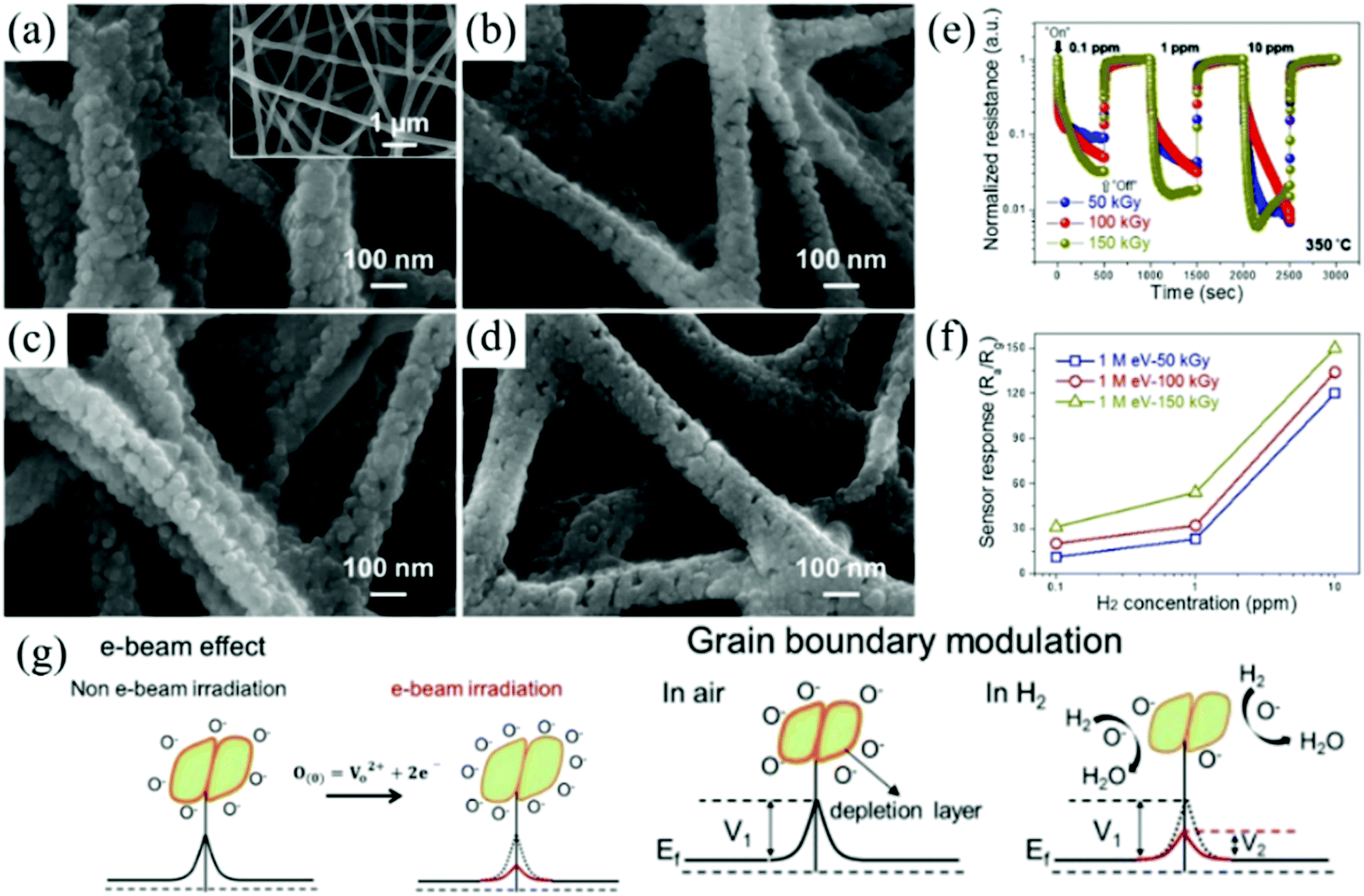 | ||
| Fig. 9 FE-SEM images of ZnO NFs irradiated at doses of (a) 0 kGy; (b) 50 kGy; (c) 100 kGy; and (d) 150 kGy; (e) normalized dynamic resistances of ZnO NF sensors irradiated at different e-beam doses to 0.1, 1, and 10 ppm H2 at 350 °C; (f) corresponding calibration curves; (g) sensing mechanism of the e-beam-irradiated ZnO NFs gas sensor12 (Copyright 2019, Elsevier). | ||
After electron beam irradiation, the structure of the material could be changed and different types of defects could be formed, such as interstitial atoms and vacancies.150 Vacancies play a key role in the electronic properties of sensitive materials and the increase in the vacancies can enhance the concentration of adsorbed oxygen on the surface, thereby improving its sensing performance.
The advantage of using high-energy radiation to modify MOx nanomaterials is that not only does it change the macro-morphology of the original material but also modulates the structural defects on the surface of the material due to the strong penetration and decomposition efficiency. It affects the excitation of the hole–electron pairs in semiconductor MOx, increasing the width of the accumulating layer and decreasing the width of the depleting layer, thus providing more adsorption sites on the surface of the material to improve the sensor performance and selectivity. These principles are also applicable to other MOx nanomaterials, which provide a new idea for the construction of a new sensing platform in the future.
Remarkably, the exposure position and area of the crystal planes also influence the performance of the sensor.189,190 Different crystal surfaces have different surface energies;191 thus, the energy required for gas adsorption on its surface also varies. Since different exposure positions and areas affect the number of oxygen vacancies in MOx, the more the oxygen vacancies, the stronger the macroscopic resistance modulation ability of the material, and the performance of the sensor will be enhanced.
Wu et al.176 prepared three kinds of ZnO nanostructures and found that with different exposure surfaces, the sensors exhibited different performances. Among them, the tower-like structure ZnO has the highest response to H2, which is due to the fact that the (0001) crystal plane of the tower-like structure ZnO is exposed the most. The (0001) crystal plane contains more oxygen vacancies than the other planes, which means that on the (0001) crystal plane, the number of adsorbed oxygens will be greatly increased, which is conducive for the improvement of the sensor performance. The defects on the surface of these three structures were analyzed by XPS and PL spectroscopy, respectively, which also proved that tower-like structure ZnO had the highest oxygen vacancy concentration. The same is true for other MOx nanomaterials, for example, the (002) crystal plane of TiO2 could enhance the response of the sensor57,192 and the (004) crystal plane of TiO2 could realize the reduction of the response time.193 Both the (001) crystal plane of the hexagonal WO3189 and the (110) crystal plane of SnO2190 could enhance the performance of the sensors. The regulation of the crystal plane engineering of the sensing materials provides new a research direction for the development of sensing materials in the future.
3.4 P-Type semiconductor metal oxide nanomaterials
P-Type semiconductor metal oxides are a class of materials whose conductivity decreases with the increase in the reducing gas. The application of p-type MOx in the field of gas sensing is more challenging because the main carrier of p-type MOx are the holes. Hübner et al.194 indicated that under the same conditions, the response of p-type was equal to the square root of n-type, as depicted in eqn (6). | (6) |
The major p-type MOx nanomaterials in H2 sensing are CuO111,195 and NiO,149,150,196 as listed in Table 6.
| Materials | Structure | c | T (°C) | LOD | Sensitivity | Response time | Ref. |
|---|---|---|---|---|---|---|---|
| LOD: limit of detection; response with different definition a: Ra/Rg, b: Rg/Ra, c: Ia/Ig, d: ΔR/Ra, ΔR = (Ra − Rg) or (Rg − Ra), e: ΔR/Rg, ΔR = (Ra − Rg) or (Rg − Ra), f: ΔI/Ia, ΔI = (Ia − Ig) or (Ig − Ia), g: ΔI/Ig, ΔI = (Ia − Ig) or (Ig − Ia), h: Ig/Ia. | |||||||
| CuO | Nano-bitter gourd | 100 ppm | 200 | 2 ppm | 175%d | 10/1016 s | 59 |
| CuO | Nanowires | 100 ppm | RT | — | 4.6%f | — | 111 |
| CuO | Nanowire | 100 ppm | 300 | — | 340b | 60/2 s | 195 |
| NiO | Nanoplates | 100 ppm | 200 | — | 90%d | 180 s | 60 |
| NiO | Thin films | 30 ppm | RT | 30 ppm | 310%d | 6/0.5 s | 149 |
| NiO | Film | 1000 ppm | 175 | — | 32.4d | 134/406 s | 150 |
| NiO | Thin films | 40 ppm | 200 | 5 ppm | 75%d | — | 196 |
| NiO | Nanosheet | 150 ppm | 250 | 10 ppm | 191%d | 150 s | 60 |
| NiO | Nanowires | 50 ppm | 400 | — | 34%d | 35/20 s (450 °C) | 197 |
| TeO2 | Nanowires | 0.5 vol% | 25/140 | 23 ppm | 28%/57%d | 100/250 s | 61 |
CuO demonstrates a promising p-type MOx nanomaterial for H2 sensing due to the hydrogen-induced metallization phenomenon.195 On the surface of CuO, the H2 molecules not only react with the oxide anions but also react with CuO to form Cu2O or Cu, based on the reactions (7) and (8).186
| H+(ads) + CuO(s) → 1/2Cu2O + 1/2H2O | (7) |
| H+(ads) + 1/2Cu2O → Cu(s) + 1/2H2O | (8) |
High-energy radiation is also widely available in the preparation of p-type MOx. Ultraviolet irradiated CuO nanowires can detect H2 at room temperature.111 Pulsed laser irradiated NiO nanofilms have higher response and faster recovery time.150
The choice of the sensing substrate will affect the performance of the sensor. Abubakar et al.149 deposited a cubic NiO film on the ITO conductive glass by RF magnetron sputtering under the annealing process. The NiO film is relatively loose due to the annealing treatment. Compared with a similar compact film, the loose film means more voids. H2 can not only react on the surface of the material but also goes deep into the interior of the material. By increasing the contact between H2 and the material, a lower concentration can be achieved and a lower optimal operating temperature can be realized. Because its loose surface can better realize the reversible adsorption and desorption of H2, the response/recovery time of the sensor is very fast, with a response time of 6 s and a recovery time of 0.5 s with a temperature of 150 °C, which is the fastest among the mono-semiconductor metal oxide nanomaterials.
To sum up, mono-semiconductor MOx nanomaterials as sensing materials realized the detection of H2 with fast response, low detection limit, and high sensitivity, which can greatly improve the performance of the sensor by controlling its morphology and structure as well as regulate the oxygen vacancies on the material surface. However, the inherent limitations hamper their further improvement; one of the most critical shortcomings is the high working temperature, which seriously impedes the practical application space of the sensor. Therefore, the realization of low-power detection is spurring researchers to explore and design new functional MOx. In the following sections, mono-semiconductor MOx decoration by noble or non-noble metals and binary, ternary, or more complicated nanostructures will be discussed in detail.
4. Metal@MOx composites for H2 gas sensor
Decorating metal nanoparticles into the MOx nanomaterials can effectively improve the performance of the gas sensors, which have received extensive attention from researchers. Decorating with ideal elements can tune the surface defects of the materials, which lead to more oxygen vacancies. Moreover, incorporating noble metal ions with high catalytic activity onto the MOx nanomaterials could form the Schottky barrier, which improves the selectivity and performance of the sensors.4.1 Synthetic strategy for M@MOx nanocomposites
There are many methods for the synthesize of metal@MOx composites, as summarized and listed in Table 7.| Materials | Method | Precursor | Solvent | Temp. time | Conv. cond. | Ref. |
|---|---|---|---|---|---|---|
| Ag–ZnO | Electrodeposition | ZnCl2, KCl, AgNO3 | H2O | 91 °C, 200 min | 250 °C, 12 h | 64 |
| Au–ZnO | Electrodeposition | ZnCl2, KCl, HAuCl4 | H2O | 85/90 °C | — | 198 |
| Cd–ZnO | Electrodeposition | ZnCl2, KCl, CdCl2 | H2O | 92 °C, 150 min | 300 °C, 11 h | 75 |
| Pd–ZnO | Electrodeposition | ZnCl2, KCl, PdCl2 | H2O | 90 °C | 250 °C, 12 h | 45 |
| Rh–SnO2 | FSP | Tin(II) 2-ethyl hexanoate, rhodium(III) acetylacetonate | Xylene | — | — | 102 |
| Pt–SnO2 | FSP | Tin(II) 2-ethylhexanoate, platinum(III) acetylacetonate | Xylene | O2: 2.46 L min−1, CH4: 1.19 L min−1 | — | 199 |
| Pt–Zn2SnO4 | FSP | Zinc(II) acetylacetonate, tin(II) 2-ethylhexanoate, platinum(II) acetylacetonate | Xylene + methanol (7 + 3) | 5 mL min−1 | — | 200 |
| Pd–ZnO | Spray pyrolysis deposition | Zn(Ac)2·2H2O, PdCl2 | — | — | 400 °C, 1 h | 201 |
| Cr–ZnO | SPT | Zn(Ac)2·2H2O | H2O | 350 °C | 450 °C, 1 h | 78 |
| Cr(NO)3·6H2O, HMT | ||||||
| Cu–CdO | SPT | Cd(Ac)2, Cu(Ac)2 | H2O | 300 °C | — | 38 |
| Mg–ZnO | SPT | Zn(Ac)2, HMT, Mg(Ac)2 | H2O | 300 °C | 200 °C | 202 |
| W–ZnO | SPT | Zn(Ac)2·2H2O, WCl6 | EtOH, H2O | 350 °C | — | 82 |
| Pd–SnO2 | Solvothermal | SnCl4 5H2O, PdCl2, NaOH | DMF | 160 °C, 15 h | 400 °C, 1 h | 203 |
| Co–ZnO | Hydrothermal | Zn(Ac)2·2H2O, HMT, Co(NO3)2 | H2O | 90 °C, 24 h | — | 77 |
| Cd–ZnO | Hydrothermal | Zn(NO3)2·6H2O, HMT, Cd(NO3)2·4H2O | H2O | 100 °C, 24 h | — | 204 |
| Nb–TiO2 | Hydrothermal | TBOT, HClO2, Nb(OCH2CH3)5 | H2O | 150 °C | 400 °C, 20 min | 205 |
| Pd–In2O3 | Hydrothermal | InCl3·4H2O, SDS, urea, PdCl2 | H2O | 120 °C, 15 h | 500 °C, 2 h | 67 |
| Rh–SnO2 | Hydrothermal | RhCl3·3H2O, glucose, SnCl4·5H2O | H2O | 200 °C, 12 h | 500 °C, 30 min | 206 |
| Rh/RhxOy | PLD | Rhodium rod target | H2O | 40 min | — | 207 |
| Pd–SnO2 | EISA | Pluronic F-127 (EO106PO70EO106), SnCl4·5H2O, PdCl2 | EtOH | RT, 24 h | 400 °C, 3 h | 208 |
| In–ZnO | CVD | Zn powder, In powder | — | Ar: 200 sccm, O2: 10 sccm | — | 209 |
| La–SnO2 | Electrospinning | SnCl2·2H2O, PVP, La(NO3)3·6H2O | DMF, EtOH | 15 kV, 20 cm | 600 °C, 3 h | 210 |
| Mg–In2O3 | Electrospinning | In(NO3)3, PVP, Mg(NO3)2·6H2O | DMF, EtOH | 15 kV, 15 cm | 600 °C, 3 h | 80 |
| Pd–ZnO | Electrospinning | Zn(Ac)2, PdCl2 | PVAc, IPA | +15/−10 kV, 0.07 ml h−1, 20 cm | 600 °C °C, 2 h | 211 |
| Ga–ZnO | Sol–gel method | Zn(Ac)2, Ga(NO3), MEA | IPA | RT, 12 h | 550 °C, 3 h | 212 |
| Pt@NiO | Sol–gel method | H2PtCl6·6H2O, stearic acid, Ni(NO3)2·6H2O, SDBS, (NH4)2CO3 | EtOH | pH = 7, 60 °C, 24 h | 500 °C, 2 h | 47 |
Electrochemical deposition is a ubiquitously useful method for depositing a coating on the surface of the substrates.213 The application of electrochemical deposition nanocomposites is more extensive and flexible for the morphology of the material and the proportion of substances in the material can be easily controlled by selecting different electrolyte solutions, different electrochemical methods, potentials, and currents during the deposition process.214
For example, Lupan et al.64 adopted a three-electrode system, in which FTO conductive glass was used as the working electrode, the deposition potential was −0.58 V, and the current density was −64 C cm−2. At 91 °C, the Ag–ZnO nanoarray was obtained by electrochemical deposition for 200 min. The diameter of the Ag–ZnO nanoarray is about 100–400 nm and the length is about 4 μm. By adjusting the deposition potential and electrolyte solution, diverse metal-doped MOx structures such as Pd–ZnO,45 Au–ZnO,198 and Cd–ZnO75 were also prepared for H2 gas sensing. The electrochemical deposition technique has broad application prospects. It can not only realize the growth of semiconductor MOx and doped particles simultaneously but can also achieve surface doping and material functionalization simultaneously. Moreover, for the preparation of materials with complex structures, electrochemical deposition technology can reduce the technical steps and achieve efficient and green synthesis.
Spray pyrolysis is the process of forming aerosol from metal salt solution under the atomization of the spraying device, precipitating a solid phase due to supersaturation under high temperature, and finally forming an ultrafine powder through particle hydrolysis, sintering, or other processes.215 With continuous development in recent decades, spray pyrolysis technology has become an important means to synthesize multi-MOx.
Spray pyrolysis has the advantages of both gas-phase and liquid-phase methods due to its special synthetic procedures.216 Spray pyrolysis uses a liquid phase solution as the precursor; thus, the stoichiometric ratio of each component of the composites can be precisely controlled. In the synthetic process of materials, the principle of vapor deposition is adopted, which can ensure high purity of the product.
A large number of M@MOx nanocomposites films can also be prepared by SPT.82,202 For example, CdO films doped with different concentrations of doped Cu were prepared on amorphous glass substrates by the spray pyrolysis technology (SPT).38 In addition, SPT can also be combined with successive ionic layer deposition (SILD) to prepare noble metal-doped MOx. SILD can realize the synthesis of noble metal clusters on the surface of MOx by controlling the number of cycles of ion deposition and the thickness of deposited nanoparticles can be controlled with high precision, which is similar to ALD. Korotcenkov et al.65 prepared Au–In2O3 thin films by SPT combined with SILD and realized the efficient detection of H2.
It is worthwhile to mention that flame spray pyrolysis (FSP) is a promising technique to prepare MOx,217 especially the noble metal-doped MOx nanomaterials.218 This is because the vapor pressure of noble metals is generally higher than that of MOx; thus, MOx are first produced in flames and then noble metal nanoparticles grow heterogeneously on their surfaces in situ. The synthesis of Rh–SnO2102 and Pt–SnO2199 composites with different doping amounts via FSP have been reported.
PLD, an emerging thin film preparation method, could realize high-quality metal–semiconductor MOx nanocomposites synthesis, whose working principle is that the plasma directed local expansion deposits a film on the substrate.219 It has been reported that rhodium-doped nanocolloidal rhodium oxide particles can be prepared in water by nanosecond pulse excitation starting from high purity rhodium targets, which is the first application of rhodium oxide/rhodium colloids in resistive gas sensors.207 However, the PLD technology can cause micron–submicron particle contamination on the surface of the film during the preparation process; thus, the uniformity of the film is poor. Moreover, PLD is a high energy-consuming method and so, it is not widely used in the preparation of semiconductor MOx.
Glancing-angle deposition (GLAD) focuses on film preparation with controllable morphology.220 The schematic of glancing-angle dc magnetron sputtering deposition is shown in Fig. 10a. The morphology of Pt–WO3 is shown in Fig. 10b. In addition to the above synthetic methods, magnetron sputtering technique can also realize the preparation of the doped MOx nanomaterials.221
 | ||
| Fig. 10 (a) Schematic of the Pt-decorated WO3 nanorod array fabricated by the glancing-angle dc magnetron sputtering deposition; (b) morphology of Pt–WO3 doped with different ratios220 (Copyright 2014, American Chemical Society). | ||
Hydrothermal or solvothermal technology is widely used in the preparation of metal–MOx nanocomposites. The target products can be obtained by mixing different salt solutions in the autoclave and treating them with high temperature and high pressure. By controlling the reaction conditions, MOx nanomaterials with different morphologies can be obtained. As for M@MOx nanocomposites, hydrothermal or solvothermal technology can be divided into two categories.
Wang et al.222 developed a versatile two-step hydrothermal method for noble metal-doped MOx composites. Briefly, ((NH4)10–H2(W2O7)6·xH2O) was used as the precursor and organic acid was used as the solvent to assist the synthesis of MOx nanomaterials. Then, noble metal nanoparticles were modified in situ on the surface of the synthesized MOx using iodide ion (I−) as the strong adsorbent, polyvinylpyrrolidone (PVP) as the capping agent, and N,N-dimethylformamide (DMF) as the solvent. Meanwhile, I− is also a morphology control agent during the synthetic process, which can realize the control of its morphology. The structure of the prepared Pd–WO3 nanoplates is shown in Fig. 11a–c. It can be seen from Fig. 11b and c that the doped Pd nanoparticles are attached to the surface of WO3, which play an important role in improving the performance of the sensor. Liu et al.223 and Xiao et al.224 also successfully synthesized Pd–WO3 nanoparticles using this method.
 | ||
| Fig. 11 (a) SEM images of Pd–WO3; (b and c) TEM images of Pd–WO3222 (Copyright 2015, Royal Society of Chemistry). (d) SEM of Rh–SnO2; (e) TEM of Rh–SnO2; nitrogen adsorption isotherms and corresponding pore size distribution (inset) of (f) SnO2 and (g) Rh–SnO2206 (Copyright 2017, Springer Nature). (h) Schematic of the synthesis of 3DOM WO3; SEM images of 3DOM samples: (i) WO3; (j) Pd/WO3 (2–1); (k) Pd/WO3 (1–1); (l) Pd/WO3 (1–2)71 (Copyright 2018, Elsevier). | ||
The hydrothermal or solvothermal method can also realize the “one-pot” preparation of M@MOx nanocomposites. This method not only shortens the reaction time but also has more advantages in terms of the economic benefits and environmental friendliness. Li et al.203 obtained SnO2 nanocomposite structures loaded with Pd NPs by the “one-pot” method. Depending on the different precursors added, Cd–ZnO,204 Co–ZnO,77 and other nanocomposites can also be prepared by the “one-pot” method. In the hydrothermal process, the added template plays a key role in the regulation of the material morphology. Hong et al.206 synthesized porous coral-like Rh-doped SnO2 nanostructures using glucose as the template; the morphology is shown in Fig. 11d and e. As seen from Fig. 11f and g, the addition of Rh can alter the pore size of the materials.
In addition, the hydrothermal method combined with other methods has been widely studied and used in the preparation of M@MOx nanocomposites. The first strategy is to prepare MOx nanoparticles by the hydrothermal method and then deposit all doped noble and non-noble metal nanoparticles onto the MOx surface through vapor deposition such as CVD225 and sputtering technology.226 Similarly, the liquid phase chemical synthesis method can also be combined with it. In this synthetic strategy, MOx obtained by the hydrothermal method can be used as substrates and the dopants are directly grown on the surface of MOx in situ by liquid-phase chemical reduction in solution to obtain composite nanostructures.
The porosity of the materials is closely related to the gas sensing properties; thus, porous structures usually exhibit more excellent gas sensing performance than solid structures. In recent years, solution template assisted methods including soft and hard templates have produced MOx nanomaterials with ordered large surface area.
In a typical synthetic process, Zhang et al.208 successfully fabricated multilayer mesoporous Pd–SnO2 thin films using Pluronic F127 as the soft template by EISA. First, the Pd-doped Sn sol was prepared, then the sol was spin-coated on the Si substrate, and then the substrate was dried at room temperature with a relative humidity of 70–80% for one week. Finally, the substrate was annealed to obtain the mesoporous structure. Interestingly, Wang et al.71 obtained three-dimensional ordered macroporous (3DOM) WO3 materials by liquid-phase reduction using PMMA microspheres as the hard templates. The schematic of the synthesis of 3DOM WO3 is shown in Fig. 11h and the SEM images with different ratios of Pd and WO3 are shown in Fig. 11i–l.
4.2 Noble metal@MOx nanomaterials for H2 sensing
Decorating noble metals onto MOx nanomaterials is one of the most effective methods to improve the performance of H2 gas sensors. It can enhance the response capacity and sensitivity of the gas sensor, reduce the optimal operating temperature, and shorten the response/recovery time due to the unique nature of the noble metal nanoparticles.Noble metal nanoparticles have stronger oxygen adsorption capacity due to the “spill-over effect”; noble metal-modified MOx can adsorb more oxygen ions and form a thick electron depletion layer on the surface of the material with higher macro-resistance. When the modified material is placed into the H2 atmosphere, the H2 molecules react with the oxygen anion and the electrons are transferred back to the semiconductor conduction band again, resulting in electron consumption. It causes the electron depletion layer to decrease sharply. This huge contrast between the background and the signal exceedingly reduces the signal-to-noise ratio of the sensor, and enhances the capacity of detection of trace H2. The high catalytic activity of noble metals themselves can reduce the activation energy required by gas adsorption, reduce the barrier required in the reaction process, and provide a possibility for the reduction of the working temperature of sensors.
Furthermore, because of the high catalytic activity, the selectivity of the sensors is considerably strengthened, especially Pd, which shows a unique property for H2 adsorption and dissociation. Finally, the modification of noble metal ions on the surface of semiconductor MOx will accelerate the electron transport rate on the surface of the materials and shorten the response recovery time.
The noble metal@MOx nanomaterials are widely used in H2 gas sensing, such as Ag, Au, Pd, Pt, Rh, and their details are listed in Table 8. It is obvious that the performance of sensors in all the aspects has been greatly improved after noble metal doping.
| Materials | Structure | c | T (°C) | LOD | Sensitivity | Response time | Ref. |
|---|---|---|---|---|---|---|---|
| LOD: limit of detection; response with different definition a: Ra/Rg, b: Rg/Ra, c: Ia/Ig, d: ΔR/Ra, ΔR = (Ra − Rg) or (Rg − Ra), e: ΔR/Rg, ΔR = (Ra − Rg) or (Rg − Ra), f: ΔI/Ia, ΔI = (Ia − Ig) or (Ig − Ia), g: ΔI/Ig, ΔI = (Ia − Ig) or (Ig − Ia), h: Ig/Ia. | |||||||
| Ag–ZnO | Nanowires | 100 ppm | RT | — | 50g | 22/11 s | 64 |
| Au–In2O3 | Nanoneedles | 1000 ppm | 450 | — | 8.5a | — | 65 |
| Au–In2O3 | Core–shell NPs | 100 ppm | 300 | 2 ppm | 34.38a | 31 s/10 min | 227 |
| Au–SnO2 | Nanoparticles | 100 ppm | 250 | 1 ppb | 25a | 1/3 s | 49 |
| Au–ZnO | Core–Shell structure | 100 ppm | 300 | 0.5 ppm | 103.9a | — | 50 |
| Au–ZnO | Films | 1000 ppm | 250 | 50 ppm | 172e | 4/68 s | 66 |
| Au–ZnO | Thin films | 1000 ppm | 150 | — | ∼75%d | — | 151 |
| Au–ZnO | Nanowires | 20 ppm | RT | 20 ppm | 2.25c | — | 198 |
| Au–ZnO | Thin films | 1200 ppm | 400 | 75 ppm | 73%e | — | 228 |
| Pd–In2O3 | Flower-like | 100 ppm | 210 | 10 ppm | 3.6a | 4/7 s | 67 |
| Pd–In2O3 | Nanoparticles | 10![[thin space (1/6-em)]](https://www.rsc.org/images/entities/char_2009.gif) 000 ppm 000 ppm |
250 | 150 ppm | 3526a | 2/180 s | 229 |
| Pd–MnO2 | Nanowalls | 100 ppm | 100 | 10 ppm | 11.4 ± 0.7a | 4 s | 37 |
| Pd–SnO2 | Microspheres | 1000 ppm | 200 | 10 ppm | 129.08a | 4 s | 203 |
| Pd–SnO2 | Mesoporous film | 1000 ppm | 275 | 50 ppm | 237.85a | 44 s | 208 |
| Pd–SnO2 | Thin film | 250 ppm | 300 | 25 ppm | 28a | 3/50 s | 230 |
| Pd–SnO2 | Nanofiber rods | 100 ppm | 160 | 0.25 ppm | 28a | 4 s | 231 |
| Pd–Sn(Sb)O2 | Nanoparticles | 0.1 vol% | 250 | — | 85.5%d | 120 s | 232 |
| Pd–TiO2 | Pd: nanocubes | 0.6 vol% | 150 | — | 40.6%d | 24/1 s | 233 |
| TiO2: nanowire | |||||||
| Pd–TiO2 | Nanotubes | 8000 ppm | RT | 5000 ppm | 92.05d | 3.8/43.3 s | 68 |
| Pd–TiO2 | Nanorods | 1000 ppm | 200 | 250 ppm | 31f | — | 225 |
| Pd–V2O5 | Thin films | 100 ppm | 100 | 2 ppm | 5.7 ± 0.3a | — | 69 |
| Pd–W18O49 | Urchin-like | 50 ppm | 100 | 50 ppm | 32a | 60 s | 70 |
| Pd–WO3 | Ordered macroporous | 50 ppm | 130 | 10 ppm | 382a | 10/50 s | 71 |
| Pd–WO3 | Thin film | 2 vol% | 80 | 100 ppm | 1.30 × 10⁴e |
<1/30 s | 234 |
| Pd–WO3 | Nanoplates | 0.1 vol% | 80 | — | 169.3b | 42.8/48.5 s | 222 |
| Pd–WO3 | Nanocomposites | 1000 ppm | RT | — | 34a | 24 s | 223 |
| Pd–WO3 | Nanotubes | 500 ppm | 450 | — | 17.6a | 25 s | 235 |
| Pd–WO3 | Nanoneedles | 500 ppm | 150 | — | 1670a | — | 236 |
| Pd–ZnO | “Nanosponge” film | 2 vol% | 80 | 0.1 vol% | 580a | 0.3/22 s | 36 |
| Pd–ZnO | Nanowires | 100 ppm | RT | — | 13100c | 6.4/7.4 s | 45 |
| Pd–ZnO | Nanowire | 400 ppm | RT | 100 ppm | 121a | — | 201 |
| Pd–ZnO | Nanofibers | 100 ppb | 350 | 0.1 ppm | 74.7a | — | 211 |
| Pd–ZnO | Nanorods | 500 ppm | 350 | — | 3.6a | — | 226 |
| Pd–ZnO | Nanorod | 1 vol% | 80 | 100 ppm | 7950f | 227/95 s | 237 |
| Pd–ZnO | Nanowires | 100 ppm | 350 | 0.1 ppm | 87.17a | — | 238 |
| Pd–ZnO | Nanorods | 250 ppm | 135 | 50 ppm | 22.5a | 26/5 s | 239 |
| Pd–ZnO | Nanorods | 1000 ppm | RT | 0.2 ppm | 91.2a | 18.8 s | 240 |
| Pd–ZnO | Pd: nanocubes | 10000 ppm |
100 | 1 ppm | 0.74d | — | 241 |
| ZnO: nanorods | |||||||
| Pt–In2O3 | Nanocubes | 15000 ppm |
RT | — | 20a | 33/66 s | 62 |
| Pt–Nb2O5 | Porous ceramics | 10000 ppm |
RT | — | 165a | 7/39 s | 63 |
| Pt–NiO | Core–shell structure | 5000 ppm | RT | 1000 ppm | 4.25a | 91/8 s | 47 |
| Pt–SnO2 | Nanosheets | 100 ppm | 350 | 0.08 ppm | 56.5a | 29 s | 72 |
| Pt–SnO2 | Thin film | 500 ppm | 110 | 2 ppm | 168e | <6/57 s | 242 |
| Pt–SnO2 | Thin film | 250 ppm | 200 | 25 ppm | 51.6a | — | 243 |
| Pt–TiO2 | Nanofibers | 700 ppm | — | 100 ppm | 400%f | — | 73 |
| Pt–TiO2 | Nanocomposites | 1000 ppm | RT | 30 ppm | 6000a | 10/20 s | 244 |
| Pt–TiO2 | Thin film | 10000 ppm |
RT | 300 ppm | 1.58 × 10⁷a |
150/280 s | 245 |
| Pt–ZnO | Thin film | 75 ppm | 300 | 75 ppm | 60%d | — | 7 |
| Rh–RhxOy | Film | 50 ppm | 200 | 75 ppm | 23e | 2/5 min | 207 |
| Rh–SnO2 | Nanoparticles | 3 vol% | 300 | — | 22170a | 6 s | 102 |
| Rh–SnO2 | Coral-like | 100 ppm | 260 | 10 ppm | 312a | — | 206 |
One of the significant advantages of noble metal doping is the reduction of the working temperature, which achieves the detection of H2 at low temperature or even room temperature. Because of the catalytic ability of noble metals, the activation energy during the reaction between materials and H2 is greatly reduced, which could further reduce the activation barrier in the reaction between the materials and H2, thereby reducing the working temperature of the gas sensor. Vijayalakshmi et al.201 prepared Pd–ZnO nanowires to detect H2 at room temperature and the sensor responded to H2 at 400 ppm up to 121 (defined as Ra/Rg). Ag–ZnO nanostructures prepared by the electrochemical deposition by Lupan et al. could also achieve efficient detection at room temperature.64
The response of the sensor highly depends on the interaction between the target gas and the surface of the material. Doping noble metal particles is quite a powerful method to enhance the capacity of the surface of the material to adsorb oxygen and it is extensively carried out to improve the response of the sensor as well as to reduce the detection limit of the sensor. Hong et al.206 synthesized Rh-doped coral SnO2 nanostructures by the hydrothermal method. The sensor exhibits a high response of 312 (defined as Ra/Rg) to 100 ppm H2 at the optimum operating temperature, which is 26 times higher than that of the undoped coral SnO2 and the detection limit of Rh–SnO2 for H2 is only 10 ppm. The composite can adsorb more reactive oxygen molecules and improve the sensing response owing to the high electron density of Rh.
Moreover, the sensor based on Pd–V2O5 can realize the sensitive and rapid detection of H2.69 Pd doping can generate active centers on its surface, which has an advantage over the adsorption of target gases and the improvement of electron transport. Moreover, Pd has a higher work function and high catalytic activity, which can bring electronic and chemical sensitization on the surface of MOx, and improve the sensor response capacity (as shown in Fig. 12a and b). In addition, the prepared Pd–V2O5 films have excellent stability and selectivity. Pd–V2O5 can maintain a high response capacity towards H2 for 3 months. Compared with other interfering gases, Pd–V2O5 has the highest response value to H2 under the optimal working conditions, which is highly satisfactory.
 | ||
| Fig. 12 (a) Schematic illustration explaining the H2 sensing mechanism of the Pd/V2O5 thin film sensor69 (Copyright 2016, Elsevier). (b) Response curve and response/recovery time of Pd–ZnO composites with different morphologies to the H2 test chart239 (Copyright 2018, Royal Society of Chemistry). (c and d) HR-TEM images of the Au/In2O3 core–shell structure; (e) dependence of the sensor response of Au@In2O3 core–shell and In2O3 NPs at different temperatures to 100 ppm H2 gas; (f) dynamic response–recovery curves at an operating temperature of 300 °C and 100 ppm H2 gas227 (Copyright 2016, Royal Society of Chemistry). | ||
After noble metal modification, the response/recovery time of the sensor is also greatly improved. Chen et al.67 prepared flower-shaped spherical Pd–In2O3 nanostructures by the hydrothermal method. The response speed is shortened and the sensitivity is enhanced. It is because after Pd incorporation, a large number of high active reaction sites and oxygen functional groups on the surface of MOx are produced, and the activation energy is minimized due to the high catalytic activity of the Pd nanoparticles, which accelerates the occurrence of the reaction.
Moreover, the effect of the morphology on the sensor performance is also applicable to noble metal-modified MOx. Tang et al.239 explored the effect of Pd NPs with different morphologies (Pd nanoparticles are cubical, spherical, and octahedral) on the gas sensing performance of Pd–ZnO nanorods. From the test results, the cubic Pd-doped ZnO nanorods have the highest sensing response capacity (shown in Fig. 12b); thus, the morphology of the doped noble metal nanoparticles will also have an impact on the sensing characteristics, which has a certain guiding significance for the preparation of sensing materials.
In order to enhance the performance of the sensors, the manner of noble metal doping has gradually changed. In most cases, noble metal particles are dispersed on the surface of MOx but sometimes, noble metals may occupy the active sites on the surface of MOx. Moreover, owing to the generally small size of noble metal nanoparticles, the phenomenon of agglomeration on the oxide surface may occur, thereby attenuating the sensor performance.
Designing core–shell structures can relieve this phenomenon due to the unique structural advantages. The existence of the core–shell structure can protect the noble metal core to the greatest extent; furthermore, the characteristics of the three-dimensional structure of the core–shell structure are more conducive for the transmission of electrons between the interfaces and to improve the response of the sensors.246 Chava et al.227 synthesized the Au/In2O3 core–shell structure by the hydrothermal method, followed by the chemical bath method. As shown in Fig. 12c and d, the performance of the Au/In2O3 core–shell structure is excellent at the optimum working temperature, and its response value and selectivity are greatly improved compared with In2O3 (Fig. 12e). In comparison with the other structures, the core–shell structure has the advantage of working temperature, response, and so on. However, due to the existence of its core–shell structure, complete H2 desorption on the material surface cannot be achieved. Therefore, in the test process, the recovery time of the sensor is sluggish (Fig. 12f); sometimes, the phenomenon of baseline drift also occurs.
High-energy radiation still plays an unparalleled role in improving the performance of sensors based on noble metal-decorated MOx nanomaterials. The principle of high energy radiation for improving the performance of sensitive materials has been discussed in Section 3.2.1; thus, it will not be repeated in this section.
For instance, under high-energy radiation, the stability of the gas sensors is improved and the response/recovery time is shortened. Zhao et al.36 activated the prepared Pd–ZnO sponge-type films under ultraviolet light at 365 nm; it can be seen from Fig. 13c and d that the stability of the gas sensors has been developed and the response time is only 0.3 s. Kim et al.211 prepared Pd–ZnO nanofibers by the electrospinning technology and activated the material under high energy radiation. As can be seen from Fig. 13a and b, with the increase in the high energy radiation, the performance of the sensor showed an upward trend and its detection limit could reach 0.1 ppm.
 | ||
| Fig. 13 (a) Sensor response versus dose rate; (b) comparison of the selectivity of non-irradiated and 150 kGy-irradiated 0.6 wt% Pd-loaded ZnO NF sensors211 (Copyright 2019, Elsevier). (c) Stability of gas sensors without UV irradiation; (d) stability of gas sensors under UV irradiation36 (Copyright 2017, Elsevier). | ||
In conclusion, noble metals could lower the working temperature, improve the sensitivity and the selectivity, as well as shorten the response/recovery time because of the synergistic or additive effect of chemical and electronic sensitization. The high catalytic activity and fast carrier transport could enhance the maximum potential of the MOx nanomaterials in H2 sensing. However, the high cost impedes the commercialization application. Therefore, to reduce the cost of sensing materials, searching for low-cost MOx nanocomposites will provide technical support for the industrialization and commercialization of sensors.
4.3 Non-noble metal@MOx nanomaterials for H2 sensing
Although noble metal-decorated MOx nanomaterials have excellent sensing response, their high costs limit the large-scale application of sensors. Inspired by noble metal doping, researchers have paid attention to the decoration of other metals. The performance of H2 gas sensing is boosted by doping metal ions, such as Cd, Co, Mg, Nb, La, Cr, W, Al, Eu, In, Ni, and Cu, as listed in Table 9.| Materials | Structure | c | T (°C) | LOD | Sensitivity | Response time | Ref. |
|---|---|---|---|---|---|---|---|
| LOD: limit of detection; response with different definition a: Ra/Rg, b: Rg/Ra, c: Ia/Ig, d: ΔR/Ra, ΔR = (Ra − Rg) or (Rg − Ra), e: ΔR/Rg, ΔR = (Ra − Rg) or (Rg − Ra), f: ΔI/Ia, ΔI = (Ia − Ig) or (Ig − Ia), g: ΔI/Ig, ΔI = (Ia − Ig) or (Ig − Ia), h: Ig/Ia. | |||||||
| Al–ZnO | Thin films | 1000 ppm | 300 | 100 ppm | 66%d | — | 74 |
| Cd–ZnO | Nanowires | 100 ppm | RT | — | 3.7d | — | 75 |
| Cd–ZnO | Nanorods | 1000 ppm | 80 | 50 ppm | 6a | 43 s | 204 |
| Co–SnO2 | Nearly spherical | 2000 ppm | 250 | — | 100a | 3/15 s | 144 |
| Co–SnO2 | Nearly spherical | 2000 ppm | 225 | — | 59.4a | 7 s | 76 |
| Co–ZnO | Nanorods | 3000 ppm | 300 | — | 99.2%f | 74/40 s | 77 |
| Cr–ZnO | Nano-whiskers array | 400 ppm | RT | 75 ppm | 133e | — | 78 |
| Cu–CdO | Cubic structure | 100 ppm | 300 | 100 ppm | 48.00%e | — | 38 |
| Eu–SnO2 | Nanoparticles | 300 ppm | 350 | 100 ppm | ∼20a | 7 s | 79 |
| Eu–SnO2 | Columnar films | 100 ppm | 250 | — | 115c | — | 247 |
| Er–SnO2 | Nanoparticles | 100 ppm | 360 | — | 28a | 11/42 s | 248 |
| In–ZnO | Thin film | 5 ppm | 300 | 1 ppm | 15%d | — | 249 |
| La–SnO2 | Nanofiber | 100 ppm | 300 | 5 ppm | 9.9a | 1/1 s | 210 |
| Mg–In2O3 | Nanotubes | 100 ppm | 150 | — | 1.55a | — | 80 |
| Mg–ZnO | Like-spherical | 400 ppm | RT | 150 ppm | ∼2.75 | — | 202 |
| Mg–ZnO | Nanorods | 200 ppm | RT | — | 30a | — | 250 |
| Mg–ZnO | Film | 200 ppm | RT | 100 ppm | 35–40a | 75/54 s | 251 |
| Nb–TiO2 | Nanotubes | 1000 ppm | RT | 50 ppm | 30.9d | 100 s | 81 |
| Nb–TiO2 | Nanorods | 1 ppm | RT | 1 ppm | 22.5%d | 288/324 s | 205 |
| Ni–TiO2 | Nanospheres | 300 ppm | RT | 100 ppm | ∼220a | 40 s | 252 |
| Ni–ZnO | Thin film | 5 ppm | 150 | — | 17.77%d | — | 253 |
| W–W18O49 | Core–shell nanoflowers | — | — | 50 ppm | — | — | 254 |
Doping non-noble metal(s) into MOx is promising. Firstly, doping could lead to a significant change in the grain size of MOx. It changes the specific surface area of the material, which can increase the effective sensing area of the nanocomposites. A large specific surface area means more gas adsorption sites, which can enhance the sensing response capacity. Secondly, elemental doping is the incorporation of elements into the lattice of MOx in the form of ion substitution. The decorated particles will replace the position of the original metal particles and cause lattice distortion. These distortions will lead to an increase in the surface defects of the materials. The presence of surface defects will introduce a large number of oxygen vacancies, which leads to an increase of the depletion layer on the surface of the composite material and a higher barrier, making the sensor more sensitive to the targeted gas and reducing the detection limit of the sensor. Finally, the presence of other metal ions can adjust the energy band structure. By modifying the MOx by changing the surface potential and the carrier concentration in the composite material, rapid charge transfer could be achieved and the detection range of the sensor can be increased.
To sum up, heteroatom doping can improve the performance of the sensor due to the ability of interfacial and surficial electron tuning. The working temperature and responsiveness of the gas sensor can also be effectively ameliorated.
5. Binary metal oxide nanostructures for H2 gas sensors
Binary metal oxide nanostructures represent one of the most promising gas sensing materials owing to the existence of heterostructures. In H2 gas sensing, MOx can be combined with MOx to form MOx nanoscale heterostructures or combined with carbon-based materials to obtain the composites to enhance the performance of the sensors. In this section, after describing the synthesis of binary MOx nanomaterials, MOx nanoscale heterostructures and MOx–carbon nanocomposites for H2 sensing are presented.5.1 MOx nanomaterial heterostructure
To achieve precise control of the composition and morphology of MOx heterostructures, there is a variety of synthetic strategies applied to the construction of heterostructures. With the continuous maturation of material preparation technology, MOx heterostructures with various morphologies and structures have been prepared for the H2 gas sensor. The synthetic methods of MOx heterostructures mainly include electrospinning technology, hydrothermal method, and thermal oxidation method, as listed in Table 10.
| Materials | Method | Precursor | Solvent | Temp., time | Conv. cond. | Ref. |
|---|---|---|---|---|---|---|
| SnO2–ZnO | Electrospinning | SnCl2·2H2O, Zn(OAc)2, PVP | DMF, EtOH | 15 kV, 20 cm, 0.05 mL h−1 | 700 °C, 0.5 h | 255 |
| SnO2–ZnO | Electrospinning | SnCl2·2H2O, Zn(OAc)2, PVP | DMF, EtOH | 15 kV, 20 cm, 0.05 mL h−1 | 700 °C, 0.5–24 h | 256 |
| ZnO–NiO | Electrospinning | ZnCl2·2H2O, Ni(Ac)2·4H2O | PVA | +15/−10 kV, 20 cm, 0.01 mL h−1 | 600 °C, 2 h | 257 |
| SnO2–ZnO | Electrospinning | ZnCl2·2H2O, SnCl2·2H2O | PVA | +15/−10 kV, 20 cm, 0.01 mL h−1 | 600 °C, 2 h | 187 |
| Co3O4–ZnO | Electrospinning | ZnCl2·2H2O, Co(Ac)2·4H2O, PVA | H2O | +15/−10 kV, 20 cm, 0.01 mL h−1 | 600 °C, 2 h | 84 |
| NiO–SnO2 | Electrospinning | NiCl2·6H2O, PVP, SnCl2·2H2O | EtOH, DMF | 12 kV, 15 cm, 1 mL h−1 | 500 °C, 3 h | 258 |
| CeO2–SnO2 | Hydrothermal | Ammonium cerium(IV) nitrate, Sn powder, NH3·H2O | H2O | 200 °C, 10 h | 500 °C, 2 h | 259 |
| SnO–SnO2 | Hydrothermal | Sn(Ac)2, PdCl2, NaOH, PEG-400, EtOH | H2O | 140 °C, 24 h | — | 39 |
| CeO2–In2O3 | Hydrothermal | In(NO3)3·4.5H2O, Ce(NO3)3·6H2O, urea | H2O | 160 °C, 12 h | 500 °C, 2 h | 85 |
| ZnO–Nb2O5 | Sol–gel method | Zn(Ac)2, PEG, NH3·H2O | H2O | — | — | 260 |
| Zn2SnO4–ZnO | Thermal evaporation | SnO2 powders, ZnO powders, C powders | — | 97 vol% Ar + 3 vol% O2 100 mL min−1 | 1000 °C, 1 h | 261 |
With the development of electrospinning technology, equipment, and application, various types of electrospinning fiber materials are constantly emerging; thus, the electrospinning technology has become one of the most active methods to prepare MOx heterostructures.262 Katoch et al.255,256 used electrospinning to synthesize a series of SnO2–ZnO nanocomposite fibers with different ratios (xZnO–(1 − x)SnO2(x = 0.01–0.50),255 0.9SnO2–0.1ZnO256) and with morphology control of the nanofibers. The annealing process is validated as an important process in the synthesis of the nanofibers by electrospinning as it can not only remove the residual organic solvents in the nanofibers to purify the nanofibers but can also increase the porosity of the nanofibers with interesting morphology to improve the sensing performance of the materials.258 A large number of MOx nanofiber heterostructures have been synthesized by the electrospinning technology, such as ZnO–Co3O4,84 NiO–ZnO,257 and SnO2–ZnO.187
Besides the electrospinning method, thermal evaporation is a fast-developing technique for the preparation of MOx heterostructures by multi-step synthesis. Combined with the hydrothermal method, Co3O4–WO3263 and ZnO–WO3264 heterostructures were obtained. Combined with the solvothermal deposition technology, the Nb2O5–TeO2 heterostructure was obtained.87
The core–shell structure could reap huge fruits because of the more effective surface areas for gas adsorption. The LD technology can deposit uniform coatings on micro/nanostructured substrates with high specific surface area, especially nanowires and nanorod core–shell structures. Park et al.265 combined thermal evaporation with the ALD technology to obtain ZnO–Nb2O5 nanorods with a core–shell structure. Further, SnO2–NiO core–shell nanowires were also prepared by the ALD technology.266 Apart from the ALD technology, it is noted that Xun et al.266 obtained highly-ordered SnO2–TiO2 nanotubes by the process of anodization and impregnation.
In addition, hydrothermal or solvothermal methods are beneficial for preparing the MOx heterostructure. The preparation is similar to the metal@MOx composites and will not be elaborated in depth here.
| Materials | Structure | c | T (°C) | LOD | Sensitivity | Response time | Ref. |
|---|---|---|---|---|---|---|---|
| LOD: limit of detection; response with different definition a: Ra/Rg, b: Rg/Ra, c: Ia/Ig, d: ΔR/Ra, ΔR = (Ra − Rg) or (Rg − Ra), e: ΔR/Rg, ΔR = (Ra − Rg) or (Rg − Ra), f: ΔI/Ia, ΔI = (Ia − Ig) or (Ig − Ia), g: ΔI/Ig, ΔI = (Ia − Ig) or (Ig − Ia), h: Ig/Ia. | |||||||
| CeO2–In2O3 | Hollow spheres | 50 ppm | 160 | 0.01 ppm | 20.65a | 1/9 s | 85 |
| CeO2–SnO2 | Nanosheets | 0.5/60 ppm | 300 | 0.5 ppm | 82/1323a | — | 259 |
| Co3O4–SnO2 | Nanoparticles | 50 ppm | 300 | 5 ppm | 20%d | — | 48 |
| Co3O4–ZnO | Nanofibers | 10 ppm | 300 | 1 ppm | 113.65d | 70 s | 84 |
| Co3O4–WO3 | Nanowires | 2000 ppm | 200 | — | 610%a | — | 263 |
| Cr2O3–Nb2O5 | Nanocubes | 2 ppm | RT | — | 5.24a | 40 s | 267 |
| CuO–TiO2 | Nanotubes | 1000 ppm | 200 | — | 2f | 7.4/6.8 s | 46 |
| CuO–Nb2O5 | Nanorods | 0.5 vol% | 300 | 0.5 vol% | 217.05%b | 161–199/163–171 s | 86 |
| In2O3–ZnO | Thin films | 50 ppm | 300: n type | — | n: 41%d | n: 53/79 s | 268 |
| 200: p type | p: 2.5%d | p: 119/123 s | |||||
| NiO–ZnO | Nanofibers | 10 ppm | 200 | 1 ppm | ∼60d | ∼50/∼90 s | 257 |
| Nb2O5–NiO | Nanoparticles | 0.05 vol% | RT | — | 1.68a | — | 29 |
| Nb2O5–TeO2 | Nanobelts | 10000 ppm |
175 | 100 ppm | 10.22a | — | 87 |
| Nb2O5–ZnO | Nanorods | 100 ppm | 300 | 100 ppm | 156%a | 21 s | 265 |
| SnO–SnO2 | Nanorods | 100 ppm | 50 | 100 ppm | 1.2a | 5/45 s | 39 |
| SnO2–NiO | Nanofibers | 100 ppm | 195 | 1 ppm | 37.15a | 12/5 s (25 ppm H2) | 258 |
| SnO2–NiO | Nanowires | 500 ppm | 500 | — | 114d | — | 269 |
| SnO2–TiO2 | Nanotubes | 1000 ppm | 250 | 20 ppm | 1410a | — | 266 |
| SnO2–WO3 | Film | 1000 ppm | 225 | 50 ppm | 29.31a | 8.4 s | 270 |
| SnO2–ZnO | Hexagonal rod | 10000 ppm |
150 | 3000 ppm | 90%d | 60 s | 83 |
| SnO2–ZnO | Nanofibers | 10 ppm | 300 | — | 168.6a | — | 255 |
| SnO2–ZnO | Nanofibers | 10 ppm | 350 | 0.1 ppm | 98.3a | 138/221 s | 256 |
| SnO2–ZnO | Nanofibers | 5 ppm | 300 | 0.05 ppm | 91a | ∼25/∼30 s | 257 |
| ZnO–WO3 | Nanowires | 5000 ppm | 200 | 100 ppm | 12.6a | — | 264 |
| ZnO@ZIF-8 | Nanorod film | 50 ppm | 250 | 5 ppm | 3.28a | — | 271 |
(i) N–N heterostructure. As early as 2013, Mondal et al.83 synthesized the ZnO–SnO2 n–n heterostructure by the solvothermal method and annealing to obtain ZnO nanorods with a diameter of ∼150 nm loaded with 50–90 nm SnO2 nanospheres. ZnO and SnO2 are both n-type semiconductors; the n–n heterojunction is formed between ZnO and SnO2. Due to the existence of the heterojunction, the sensor's response capacity to H2 and the response recovery time are greatly improved. In the heterojunction, electrons can transfer from SnO2 (Φ = 5.2 eV) to ZnO (Φ = 4.9 eV). In the prepared ZnO–SnO2 composite structure, two depletion layers are formed, one on the surface of a single grain and the other on the heterojunction surface of ZnO–SnO2. The presence of two depletion layers promotes the adsorption of a higher concentration of oxygen on the sensor surface to a greater extent, which provides more reaction sites for H2. Therefore, the sensor exhibits a higher resistance in the air and the change in the resistance becomes more obvious when exposed to H2, leading to a greatly improved sensor response.
Katoch et al.255,256 synthesized ZnO–SnO2 nanofibers by the electrospinning technology and proposed a bifunctional sensing mechanism of the composite nanofibers. The basic principle of this mechanism is to improve the performance of H2 sensor based on the combination of the homogeneous interface of SnO2–SnO2 and the heterogeneous interface of ZnO–SnO2 (Fig. 14a and b). In the research process, Katoch et al. optimized the ratio of ZnO and SnO2. By preparing different ratios of the ZnO–SnO2 composite and testing under the same conditions, it was found that when the ratio of Sn:Zn was 9:1, the sensor had the greatest performance, which can detect H2 at even 0.1 ppm concentration (Fig. 14c–e). This is because when the ratio is 9:1, the grain size of the composite heterojunction is the smallest (Fig. 14f).
 | ||
| Fig. 14 (a) Mechanism 1: reducing gas effect at the SnO2–SnO2 homo interfaces; (b) mechanism 2: metallization effect at the SnO2–ZnO heterointerfaces; (c) summary of the sensor responses of the SnO2–ZnO composite nanofibers; (d) sensor responses of the SnO2–ZnO composite nanofibers to 0.1 ppm of H2 with different ZnO contents; (e) the response of SnO2–ZnO nanocomposites for 0.1–10 ppm of H2; (f) the grain size of the different nanofibers analyzed in this study255 (Copyright 2015, American Chemical Society). | ||
Moreover, if the content of ZnO is very high, contact will occur between the ZnO nanoparticles and metal–metal contact will be formed between two adjacent ZnO nanoparticles, which reduces the modulation ability of the resistance of the nanocomposites. On the other hand, if Zn is too low, the number of ZnO–SnO2 heterojunctions will be reduced, the effect of metallization will also be reduced, and the resistance modulation ability will also be reduced. The proposed bifunctional sensing mechanism provides theoretical support for the preparation and application of ZnO-based heterostructures in the future.
An interesting phenomenon was found by Pati et al.,268 in which In2O3–ZnO thin films prepared by the sol–gel method could undergo transition from n-type to p-type during the detection of the gas at a certain temperature. Below 200 °C, the sensor produces a p-type response to H2, while above 200 °C, the sensor produces an n-type response to H2. The response diagram of the sensor to the same concentration of H2 at 200 °C and 300 °C is shown in Fig. 15a and b.
 | ||
| Fig. 15 Resistance transients of indium-doped ZnO thin film gas sensor recorded in the presence of various H2 gas concentrations: (a) at 300 °C showing n-type behavior and (b) at 200 °C showing p-type behavior268 (Copyright 2014, Elsevier). (c) SEM image of the CeO2–In2O3 hollow sphere; (d) CeO2–In2O3 gas sensor response and recovery curve at 160 °C to 100 ppm H2; (e) gas sensor reversibility at 160 °C; (f) dynamic response and recovery curve of the prepared gas sensor to ppb level H2 detection; (g) long-term stability85 (Copyright 2018, Elsevier). | ||
This phenomenon occurs due to the reversal of carriers. Since the surface conduction of semiconductor oxides is caused by the joint action of electrons and holes, most of the changes in the carrier density will lead to the reversal of the type of movable carriers on the surface. When the electron concentration is less than the hole concentration, the transition from “n” to “p” occurs.
Researchers also regulated the micro-morphology of the n–n heterostructure to obtain a better sensing response. Hu et al.85 synthesized 0.1–1.5 μm CeO2–In2O3via the hydrothermal method. The structure of In2O3 hollow microspheres and its SEM images are shown in Fig. 15c. Compared with other nanostructures, the three-dimensional hierarchical system can significantly enhance the sensing characteristics of the gas, which is conducive for gas adsorption and desorption. The high specific surface area of the hollow structure and the synergistic effect of the heterogeneous structure make the sensor exhibit excellent H2 sensing ability, along with good repeatability and long-term stability (Fig. 15e). The detection limit of the sensor can reach 10 ppb (Fig. 15f) and the response recovery time is only 1/9 s (Fig. 15d). The sensor is tested again after ageing for two months and the maximum deviation of the sensor response measured during the whole sensing cycle is less than 2% (Fig. 15g). Similarly, other n–n heterostructures for the sensitive sensing of H2 such as CeO2–SnO2,259 ZnO–WO3,264 and Nb2O5–ZnO265 have also been reported.
(ii) P–N heterostructure. The P–N heterostructure is composed of different types of semiconductor materials; thus, the p–n heterostructure has a higher barrier than the n–n heterostructure.272 The p-type semiconductor has a high hole concentration, while the n-type semiconductor has a high electron concentration; at the interface of junction, the electrons and holes recombine at the interface of the two semiconductors, forming a space charge region, leading to an increase of the resistance of the composite in air. It enhances the response capability of the sensors effectively.
Shanmugasundaram et al.39 synthesized SnO/SnO2 nanocomposites in an autoclave using the “one-pot method”. The nanoparticles self-assembled into layered structures similar to nanorods during the reaction and further aggregated to form a loose cubic morphology, which finally transformed into dense microprism structures, each with a particle size of 8–10 nm. The heterogeneous interface between SnO and SnO2 helps to accelerate the transfer of free electrons from SnO2 with high power functions to SnO, thereby improving the sensor response to low concentrations of H2. Other p–n heterostructures such as Nb2O5–NiO29 and Cr2O3–Nb2O5267 could both realize the detection of low concentrations of H2 at room temperature.
At present, most of the latest work is focused on improving the sensitivity and response/recovery of the H2 gas sensor by reducing the grain size, expanding the specific surface area, and improving the gas accessibility. However, improving the selectivity of the H2 gas sensor is still a major hurdle in this area.
It is found that the selectivity can be regulated by the modulation of the barrier height in the heterojunction through the asymmetric gas sensing reactivity of heteromaterials.48,273 Hu et al.48 prepared the p-Co3O4/n-SnO2 composite at different Co/Sn molar ratio by the simple soaking calcination method. The composite with different proportions showed peculiar performance. As seen from Fig. 16a, when the molar percentage of Co/Sn was low, the sensor showed n-type sensing response to 50 ppm H2; however, when the molar percentage of Co/Sn was high, the sensor showed p-type sensing response. The sensing mechanism is shown in Fig. 16b and d. When the molar percentage of Co/Sn is low, most of the junctions formed at the SnO2/SnO2 boundary are homojunction. SnO2 plays a leading role in the resistance modulation of the heterostructures; therefore, the composites show an n-type response to H2. However, in the case of high molar percentage of Co/Sn, in addition to SnO2–SnO2 homojunction, many SnO2/Co3O4 heterojunctions are formed at the same time (mechanism diagram is shown in Fig. 16c, e and f). The formed p–n heterostructure will increase the resistances of the Co3O4/SnO2 composites sharply. After contacting H2, SnO2 reacts rapidly with H2 and electrons are sent back to the conduction band of SnO2, resulting in a decrease in the bending of the conduction band as a result of the high reactive activity to H2. On the other hand, Co3O4 has little sensitivity to H2; thus, the conduction band of Co3O4 remains almost unchanged. Consequently, the barrier height of the heterostructures is increased instead of decreasing, leading to an increase in the resistance. Unlike H2, other gases can react with both SnO2 and Co3O4 so that the height of the barrier decreases. The method of modulation of the barrier height in the heterojunction will become an indispensable tool for developing the selectivity of the sensors.
 | ||
| Fig. 16 (a) Co/Sn-10% dynamic resistance curve of typical H2, CO, NH3, and H2S reducing gas; (b–f) Co3O4/SnO2 composite sensing mechanism diagram48 (Copyright 2017, Elsevier). | ||
The heterostructure can significantly improve the sensor performance and reduce the detection limit of the sensor due to its extremely high chemical reaction activity as well as the presence of a large number of oxygen vacancies at the interface. Researchers can also achieve excellent selective sensor preparation by adjusting the barrier height of the heterostructures; however, much progress is still needed to reduce the working temperature of the gas sensor.
5.2 MOx–carbon nanocomposites
Graphene is the most active unit of carbon nanomaterials due to its unique 2D structure, large specific surface area, and excellent electron transport ability, which has attracted extensive attention from researchers.274 The preparation procedure of graphene–MOx nanocomposites in H2 gas sensing includes two main steps: firstly, the graphene structure is prepared by gas-phase methods such as CVD or liquid-phase Hummers’ method, and then the MOx nanomaterials is compounded with it.275
Kamal et al.276 employed graphene oxide (GO) and nickel dihydrazine benzoate as a precursor to prepare graphene-loaded nickel oxide (G/NiO) hybrid materials by the chemical method, as described in the flow chart (Fig. 17a). Briefly, at first, the improved “Hummers’ method” was used to obtain the graphene structure, then L-ascorbic acid was used to reduce graphene, and finally, nickel dihydrazine benzoate was mixed with graphene in the liquid phase to obtain the composite structures. The complex surface contains a large number of groups, which interact with the surface of graphene, adsorb on the surface of graphene through a covalent bond, and then decompose by the loss of N2H4, CO2, and H2O through low-temperature heat treatment. Thus, the formed NiO was deposited on G without further purification to obtain G/NiO.
 | ||
| Fig. 17 (a) Synthetic route for the preparation of the G/NiO hybrid276 (Copyright 2016, Elsevier). SEM (b) and TEM (c) images of SnO2 graphene (S-G) composites277 (Copyright 2016, Elsevier). (d) Structure and molecular weight of the PS-b-P4VP used in this study, and the schematic representation of C-doped WO3 nanostructure preparation with PS-b-P4VP89 (Copyright 2015, Royal Society of Chemistry). | ||
The solvothermal method can obtain MOx nanomaterials with good crystal form and uniform particle distribution; meanwhile, graphene oxide can also be reduced to rGO. Thus, graphene–MOx can be prepared directly. Zhang et al.277 synthesized SnO2 graphene (S-G) composites by a “one-pot” hydrothermal method. Rod-like SnO2 was growth on the graphene substrate (Fig. 17b and c). Graphene-loaded TiO2 was prepared by the sol–gel method using titanium tetra-isopropoxide as the precursor.278 Hydroxyl groups on the surface of graphene could also act as nucleation centers of the metal oxide particles, loading more inorganic nanoparticles on the surface of graphene.
Notably, the use of block copolymers can lead to highly regular and periodic structures of materials, which are ideal candidates for the preparation of highly ordered nanoarrays. Liu et al.89 synthesized C–WO3 nanoparticles with different morphologies using a co-block polymer compound PS-b-P4VP as the template. The processes are shown in Fig. 17d.
| Materials | Structure | c | T (°C) | LOD | Sensitivity | Response time | Ref. |
|---|---|---|---|---|---|---|---|
| LOD: limit of detection; response with different definition a: Ra/Rg, b: Rg/Ra, c: Ia/Ig, d: ΔR/Ra, ΔR = (Ra − Rg) or (Rg − Ra), e: ΔR/Rg, ΔR = (Ra − Rg) or (Rg − Ra), f: ΔI/Ia, ΔI = (Ia − Ig) or (Ig − Ia), g: ΔI/Ig, ΔI = (Ia − Ig) or (Ig − Ia), h: Ig/Ia. | |||||||
| C–SnO2 | Spherical | 2 vol% | 50 | — | 6%d | — | 279 |
| C–WO3 | Nanodots | 60000 ppm |
RT | — | 114g | 162/108 s | 89 |
| Graphene–In2O3 | Nanocrystals | — | 250 | 250 ppm | — | — | 90 |
| Graphene–NiO | Thin paper like | 2000 ppm | 200 | — | 52.4%d | — | 276 |
| Graphene–SnO2 | Flower-like | — | 150 | — | 87.2a | — | 277 |
| Graphene–TiO2 | Thin films | 0.5 vol% | 125 | 0.5 vol% | 19%f | 16/61 s | 278 |
| Graphene–ZnO | Nanotubes | 100 ppm | RT | 10 ppm | 28.08a | 30/38 s | 280 |
| Graphene–ZnO | Nanosheet with nanorods | 200 ppm | 150 | 10 ppm | 3.5a | 22/90 s | 281 |
| rGO–CuO | Film | 1500 ppm | RT | 10 ppm | ∼12d | 80/60 s | 282 |
| rGO–NiO | Nanosheet | 1 vol% | 18 | 0.5 vol% | 0.64d | 28/142 s | 91 |
| rGO–ZnO | Nanofiber | 10 ppm | 400 | 100 ppb | 2524a | 0.9/3.5 min | 283 |
| CNT–Co3O4 | Circle-shaped | — | RT | — | — | 21/26 s | 88 |
| CNT–SnO2 | Nanoparticles | 4 vol% | 200 | 0.1 vol% | 84%d | 120 s | 284 |
| CNT–ZnO | Nanorods | 1000 ppm | 300 | — | 66%d | — | 285 |
| CNF–ZnO | Nanofibers | 100 ppm | 150 | 1 ppm | 73.54%d | 29.66/326.22 s | 92 |
Since graphene was separated from graphite in 2004, it has attracted extensive attention from researchers because of its huge specific surface area, good stability and conductivity, and high mechanical strength.286,287 Pure graphene has poor sensitivity to H2 and needs to be combined with other materials to make it sensitive.274,280 Graphene–MOx nanocomposites have significant advantages in detecting H2.288,289 Firstly, the graphene surface contains a large number of oxygen functional groups, which make it possible to adsorb more H2, thereby enhancing the resistance modulation ability of the composites. Secondly, the wide specific surface area of graphene and the surface defects existing in the graphene material itself provide huge reactive active sites for the adsorption and reaction of gases and the attachment of MOx nanomaterials on its surface.91,290 The presence of these reactive active sites can not only improve the sensor capability of the sensor but also enhance the stability and repeatability of the gas sensor. Finally, graphene has good conductivity and high carrier mobility, which can accelerate the conduction of electrons on the surface and inside the composite materials;90,276 also, the improvement of electron conduction efficiency can shorten the response/recovery time of the sensor. These characteristics can reduce the detection temperature, and improve the selectivity and sensitivity.
Ren et al.91 prepared NiO@rGO nanostructures by freeze-drying combined with heat treatment. The SEM and TEM images of the NiO@rGO nanocomposites are given in Fig. 18a and b. It can be found that there are some wrinkles on the nanocomposites and a large number of NiO nanoparticles are uniformly distributed on the surface of rGO. The material-modified sensor has excellent performance with a relative response of 0.64 (defined as ΔR/Ra) to 1 vol% H2. This is because both NiO and graphene are p-type semiconductor materials; thus, p–p heterojunctions are generated on the surface of the NiO@rGO nanocomposites, which can increase the number of holes and its macro resistance. When exposed in H2 atmosphere, reactive oxygen anions produced by heterojunctions will react with H2 rapidly; coupled with the internal high load of graphene, the electrons will be immediately released to the metal surface, which will greatly increase the ability of resistance modulation, thus achieving a rapid, efficient, and sensitive detection of H2.
 | ||
| Fig. 18 (a) SEM image; (b) HRTEM image of the NiO@rGO nanocomposite; (c) the NiO@rGO sensor operating at a temperature of 50 °C and RH 40%; the response curve of the corresponding response when exposed to various H2 concentrations under the condition of 18 °C; (d) linear fitting diagram; (e) schematic diagram of the possible sensing mechanism of the NiO@rGO nanocomposite exposed to H2 gas, energy band diagram of NiO@rGO, and the hole transfer between NiO and rGO91 (Copyright 2018, Elsevier). | ||
The performance of the sensor is shown in Fig. 18c and d. Kamal et al.276 also studied the H2 gas sensing properties of the NiO/rGO nanostructures. They found that the high porosity of graphene and a large number of single active sites on graphene are the key factors to improve the performance of the sensor. Moreover, due to the strong electronic transmission ability of graphene, the close contact between NiO and graphene will lead to electronic interaction between the two materials, which may lead to the enhanced charge separation of the composite material, thereby enhancing the performance of the sensor.
Compared with the composite of p-type semiconductor and graphene, the composite of n-type semiconductor nanostructure and graphene is more widely used in gas sensing because the p–n junction can be formed.
For example, the GO/ZnO composite prepared by Anand et al.281 achieved a reduction in the sensing temperature and the sensor exhibited higher performance at lower temperature compared with the corresponding bare ZnO. It is because graphene interacts weakly with the ZnO nanostructures through weak van der Waals force; thus, it can maintain its original high carrier mobility in the GO/ZnO composites. Lamellar graphene as a substrate provides a wide 3D network for the composite materials, which makes interconnection between the ZnO nanorods closer. The surface defects and functional groups of graphene themself can also serve as high-energy adsorption sites for gas molecules. At lower temperatures, H2 can realize the adsorption, reaction, and desorption processes on the surface of the material, thus reducing the detection temperature and realizing low power detection. The sensor can realize a detection limit of 10 ppm at a low temperature.
There are also some H2 gas sensors based on graphene-based composite nanostructures such as p-TiO2/n-graphene278 and (rGO)–CuO282 sandwich structures, which also achieve low power detection of H2 due to the synergistic effect of metal oxide nanoparticles and the graphene structure.
In addition to lowering the working temperature of the sensor, graphene has also contributed significantly to the improvement of the performance of the H2 sensor. Kathiravan et al.280 prepared a novel ZNT/G nanohybrid structure by combining the hydrothermal route with CVD. At room temperature, ZNT/G shows excellent performance to H2 at low concentration and has good repeatability, strong stability, as well as ultra-fast response and recovery to H2. Mansha et al.90 also achieved the enhancement of the H2 sensing performance by the hydrothermal synthesis of the In2O3/graphene heterostructure.
Other carbon materials such as carbon nanoparticles, carbon nanotubes, and other composites also have a strong sensing performance after combining with MOx. It has been reported that the narrower the bandgap of the C nanoparticle-doped metal oxides, the lower the energy required for the transition of electrons from the valence state to the conduction band; thus, it is easier to realize gas sensing detection at a low power. The hexagonal C–WO3 nanorod arrays prepared by Liu et al.89 have a unique performance as the nanoarrays were interconnected by ultrathin carbon films because of a new conductive path. When H2 is encountered, the conductivity modification of each C-doped WO3 nanoparticle will be rapidly transferred through this new conduction pathway, thus achieving an improved hydrogen response. Also, because the work function of WO3 (4.30 eV) is lower than that of C (4.81 eV), at the heterogeneous interface, electrons are transferred from the C-doped WO3 nanoparticles to the carbon film so that they accumulate at the carbon film. When H2 enters, the resistance changes dramatically, which enhances the performance of H2 sensing. Bhatnagar et al.279 studied the behavior of C-doped SnO2 nanoparticles in gas sensing. They found that the material exhibited p-type sensing behavior for H2, n-type for ethanol, and achieved highly selective detection for H2.
Other carbon nanomaterials with different morphologies, such as carbon nanofibers92 and carbon nanotubes285 could pose high sensitivity to low concentration H2 after combination with MOx nanomaterials.
In conclusion, the performance of the sensor can be enhanced effectively by combining carbon nanomaterials. The surface defects of graphene itself greatly increase the active adsorption sites of the gases and the existence of heterostructures after compounding with MOx nanomaterials effectively improves the electron transport kinetics. The carbon nanotube structure can attach more active particles due to its porous structures, which enhances the contact with the target gas. Carbon particle doping can sensitize the sensor by changing the band structure of the MOx nanomaterials.
6. Ternary or more complicated nanostructures for H2 gas sensors
There is much potential for the utilization of ternary or more complicated nanostructures as sensing materials due to the more synergistic effects among the different elements in the nanocomposite. A few quintessential synthetic strategies and the application in H2 sensing are given in this section, and at the end of this section, some flexible H2 gas sensors based on polymer/MOx are included.6.1 Synthetic strategy for ternary or more complicated nanostructures
A few methods for the preparation and tailoring of ternary or more complicated nanostructures have been reported in the past. In the preparation process of materials, it is more necessary to select the combination of different methods to achieve the morphological control of composites and the precise control of the stoichiometric ratio of the components. The synthetic strategies are summarized in Table 13.| Materials | Method | Solvent | Temp., time | Conv. cond. | Ref. |
|---|---|---|---|---|---|
| CoO/Co3O4/WO3 | One-step hydrothermal | H2O | 180 °C, 24 h | 600 °C, 6 h | 291 |
| Pd–SnO2–MoS2 | Multistep hydrothermal | H2O | 200 °C, 24 h; 120 °C, 12 h; 180 °C, 16 h | 700 °C, 2 h | 94 |
| Pt–TiO2–MoS2 | Multistep hydrothermal | H2O | 180 °C, 24 h; 200 °C, 24 h | 400 °C, 1 h | 292 |
| Pd/WO3–ZnO | Reactive DC magnetron sputtering technique | Ar:O2 (4:1) |
WO3: 60 W, ZnO: 50 W, Pd: 30 W | — | 293 |
| rGO–Ni–ZnO | Ni–ZnO: RF sputtering techniques rGO: Hummers’ method | — | 50 W, 25 sccm, 600 °C 2 h, 1.5 × 10⁻² mbar | — | 96 |
| Pd–Al2O3–TiO2 | Al2O3–TiO2: ALD | Carrier gas: Ar | — | — | 93 |
| Pd: e-beam evaporation | |||||
| Pd/TiO2/ITO | TiO2/ITO: spray deposition method | — | Deposition pressure: 10–5 mTorr | 300 °C, 2 h | 294 |
| Pd/TiO2/ITO: electron beam deposition | |||||
| Pd–ZnO–BN | ZnO: vapor growth | Vapor growth: Ar and O2 ALD: Ar | ZnO: 950 °C, 1 h | — | 105 |
| BN: 750 °C, 40 cycles | |||||
| Pd BN: ALD | Pd: 220 °C, 200 cycles |
The hydrothermal method still withstands the precise control of each component in multicomponent materials. In this regard, the size and morphology of each component can be effectively controlled, and the product has good dispersion. For example, Luo et al.292 synthesized the Pt–TiO2–MoS2 composite nanostructures by a two-step hydrothermal method and then annealed it by blending with Pt precursors to obtain ternary composite structures. In short, TiO2 was synthesized using HF and TBOT as the precursors in a typical hydrothermal way. Then, the synthesized TiO2 NPs were used as raw materials, mixed with sodium molybdate dihydrate and thioacetamide in solution, and the TiO2–MoS2 composite was again obtained hydrothermally. To generate such a composite is relatively simple. Mixing TiO2–MoS2 and chloroplatinic acid in absolute ethanol, a uniform paste is obtained after ultrasonication and annealing at 400 °C; then, a ternary composite structure could be obtained. Zhang et al.94 also used a multistep hydrothermal method to obtain the Pd–SnO2/MoS2 composites.
The synthesis of multiple composites doped with noble metal nanoparticles includes mainly two steps: the synthesis of MOx nanomaterials by liquid-phase methods and then the decoration of noble metal nanoparticles onto the surface of MOx nanomaterials by vapor deposition. Hassan et al.95 prepared bi-noble metal-doped ternary composites, Pt/Pd–ZnO, using a combination of liquid and gas-phase synthesis methods. In a nutshell, vertically aligned ZnO nanorods were obtained by the template-assisted method and the Pt/Pd structure was synthesized by the PLD technology with high purity Pt and Pd as the targets.
6.2 Ternary or more complicated nanostructures for H2 sensing
Ternary or more complicated nanostructures are considered to be better for detecting and monitoring H2 as compared to others because they can introduce more active sites, which are beneficial for gas sensing sensitization into the material to amplify the gas sensing signal and improve the selectivity, stability, and repeatability. The characteristics and properties of different kinds of these composite materials to H2 are summarized and listed in Table 14.| Materials | Structure | c | T (°C) | LOD | Sensitivity | Response rime | Ref. |
|---|---|---|---|---|---|---|---|
| LOD: limit of detection; response with different definition a: Ra/Rg, b: Rg/Ra, c: Ia/Ig, d: ΔR/Ra, ΔR = (Ra − Rg) or (Rg − Ra), e: ΔR/Rg, ΔR = (Ra − Rg) or (Rg − Ra), f: ΔI/Ia, ΔI = (Ia − Ig) or (Ig − Ia), g: ΔI/Ig, ΔI = (Ia − Ig) or (Ig − Ia), h: Ig/Ia. | |||||||
| Pd–Al2O3–TiO2 | Thin film | 5 ppm | 450 | 5 ppm | 15%f | — | 93 |
| Pd–In2O3–ZnO | Nanofibers | 50 ppb | 350 | 0.05 ppm | 172a | — | 295 |
| Pd–SnO2–MoS2 | Nanosheets | 30 ppm | RT | 30 ppm | 0.4%d | 5 s | 94 |
| Pd–TiO2–ITO | Films | 100 ppm | RT | 25 ppm | 35e | 15 s | 294 |
| Pd–WO3–ZnO | Thin films | 100 ppm | 200 | 10 ppm | 16.8a | 16/62 s | 293 |
| Pd–Zn2SnO4/ZnO | Nanowires | 1000 ppm | 400 | — | 15.6a | 2–4 min/5 min | 296 |
| Pd–ZnO–BN | Nanowires | 10 ppm | 200 | 0.5 ppm | 12.28 ± 0.61a | 160/90 s | 105 |
| Pd–ZnO–NiO | ZnO: nanorods | 100 ppm | 225 | 2 ppm | 72%d | — | 118 |
| NiO: nanoplates | |||||||
| Pt–Pd–ZnO | Core–shell nanorod clusters | 10000 ppm |
100 | 0.2 ppm | 58%d | 5 s | 95 |
| Pt–Pd–ZnO | Nanorods | 10000 ppm |
100 | 0.2 ppm | 69.8d | 5/76 s | 297 |
| Pt–TiO2–MoS2 | Flower-like | 500 ppm | 100 | 50 ppm | 47.09%d | 2.5/6.17 min | 292 |
| Pt–Au–ZnO | Nanorods | 250 ppm | RT | 50 ppm | 25a | 115 s | 298 |
| Pt/F-MWCNTs–SnO2 | Nanotubes | 0.05 vol% | RT | 0.05 vol% | 5.4%d | 300 (1 vol% H2) | 299 |
| Pt/F-MWCNTs/TiO2 | — | 0.05 vol% | 25 | — | 3.8%d | —/20 s | 97 |
| rGO–Ni–ZnO | — | 100 ppm | 150 | 1 ppm | 63.8%d | 28 s | 96 |
| rGO/Au/ZnO | — | 500 ppm | RT | — | 96d | 8/612 s | 300 |
| rGO/Nb–TiO2 | — | 120 ppm | 200 | — | 28.4d | 930/≦300 s | 301 |
| rGO–Ni–ZnO | rGO: nanosheet | 50 ppm | 150 | 1 ppm | 29.9%d | 70/180 s | 302 |
| Ni–ZnO: nanowires | |||||||
| rGO–Pd–ZnFe2O4 | Nanoparticles | 1000 ppm | RT | 50 ppm | 29.7%d | 18/39 s | 303 |
| UNCD–MoS2–ZNRs | Nanorod | 100 ppm | RT | 50 ppm | 50.3a | 8/12 s | 304 |
| PAN–TiO2–SnO2 | Spherical | 0.8 vol% | 27 | — | 6.18a | 245/57 s | 296 |
| Pt–IGZO | Thin films | 0.01 vol% | RT | 100 ppm | 100f | ∼300 ms/30 s | 305 |
Compared with a single noble metal, bi-noble metal nanoparticles exhibit different adsorption and catalytic properties due to its geometrical and electronic effects. For example, Fan et al.298 used bi-noble metal-doped Pt–Au@ZnO ternary nanostructures as sensing materials for H2 detection. The morphology of Pt–Au@ZnO is shown in Fig. 19a and b. The sensor can respond to H2 at the ppm level at room temperature. In terms of the structure, after doping bi-noble metals, isolated Au and Pt nanoparticles will be formed on the surface of the composite, resulting in highly active sites, thus increasing the adsorption and catalytic activity of bi-noble metal nanoparticles that enable the strong adsorption of H2 on the surface of the composite. Regarding electron transport, the presence of bi-noble metal nanoparticles will accelerate the electron transport rate and reduce the sensing response time. The response range of the Pt–Au@ZnO nanocomposites to H2 is relatively high. As shown in Fig. 19c, this material can detect H2 in the concentration range of 50–2000 ppm and the response signal has a good linear relationship. Moreover, the sensor has a good selectivity (Fig. 19d).
 | ||
| Fig. 19 (a and b) ZnO nanorods loaded with Pt–Au nanoparticles; (c) sensor response to different concentrations of H2; (d) the gas sensing response of samples to different gases at 130 °C298 (Copyright 2017, Elsevier). (e) SEM image of the Pt/Pd–ZnO NR cluster; (f) TEM image of the Pt/Pd–ZnO core–shell structure; (g) Pt/Pd-response/recovery time characteristic diagram of ZnO NRs/Si exposed to 10000 ppm H2 at 100 °C; (h) transient response of the as-fabricated sensor under different humidity at 100 °C. (inset) Enlargement of the curve within the 0.2–1000 ppm range of H2 concentration; (i) histogram of selectivity of the ZnO NR clusters and Pt/Pd–ZnO NRs clusters to various test gases95 (Copyright 2017, Elsevier). | ||
To further improve the sensing performance of the sensor, Hassan et al.95 prepared Pt–Pd nanomaterials with a core–shell structure. The selectivity of the sensor is also greatly enhanced due to the presence of the noble metal compared with the bulk materials. The core–shell structures of bi-noble metals have shown different adsorption characteristics for H2 due to their different structures and electronic states. As the Pt–Pd core–shell structure is uniformly covered with a thin layer on the surface of the ZnO nanorods (Fig. 19e and f), when the sensor is exposed to the H2 atmosphere, H2 can easily penetrate through the Pt–Pd structure to reach the surface of the ZnO nanostructures. The sensing reaction occurs at the interface and the signal is increased.
Due to the high hydrophobicity and low surface energy on the surface of the material, the grain size and the grain spacing become smaller, which leads to particle contact between adjacent particles in the H2 atmosphere, thus increasing the number of shortest current paths, resulting in shorter sensor response/recovery time (Fig. 19g) and the sensor can realize the response to H2 under high humidity conditions (Fig. 19h). Meanwhile, the sensor also has excellent selectivity for H2 (Fig. 19i).
Besides, bi-noble metal modified MOx nanocomposites can also be used for the preparation of flexible devices,297 which provides theoretical support for the application of wearable devices. In addition to bi-noble metal doping, some bimetal-doped metal oxide composite structures such as Pt/Nb–TiO2/Pt306 and Ga–Pd/ZnO240 also have a high response to H2.
Because of a large specific surface area and special physicochemical properties, 2D materials are often used in multicomponent composite structures to “connect” other components or to load multicomponent substances. Among them, graphene is still widely used in ternary composites due to the wide specific surface area and abundant surface defects. Bhati et al.96 prepared rGO–Ni–ZnO composites by RF sputtering. rGO is a p-type semiconductor and can form various heterostructures with Ni-doped ZnO. The intrinsic properties of rGO improve the active sites for oxygen atom adsorption and increase the loading of oxygen on the material surface.
As mentioned above, rGO extracts electrons from ZnO, which will increase the thickness of the depletion layer and increase the material to macro. The modulation ability of the apparent resistance enables the efficient and sensitive detection of H2. Abdollahi et al.302 also synthesized the rGO–Ni–ZnO ternary composite by the hydrothermal method, which also has high sensitivity and selectivity for H2. At the working temperature of 150 °C, the sensor response value to 50 ppm of H2 is 29.9% (refined as ΔR/Ra). The role of graphene in ternary composites is to serve as the substrate of the sensing materials, which could provide reactive active sites, improve the resistance modulation ability of the composites, and thus improve the performance of the sensors.
MoS2, another 2D layered lamellar materials with graphene shape, is considered as a promising gas sensing material due to its specific surface area.70 MoS2 has good electrical properties. Unlike graphene, MoS2 has a bandgap ranging from 1.2 to 1.8 eV due to different microstructures, which provides a broad space for researchers to regulate it. MoS2 with a wide specific surface area as a substrate can act as a carrier for the material and gas adsorption, and can bring more surface-active sites so that the sensor can obtain better performance. At the same time, the heterostructures generated during the composite with metal oxides also contribute to the improvement of the sensor performance.
Zhang et al.94 prepared the Pd–SnO2/MoS2 ternary hybrid for H2 gas sensing. Due to the synergistic effect of ternary nanostructures and the regulation of the barrier by electron transport, the sensor can detect H2 at room temperature with exceedingly good performance. The characterization test analysis showed that the Pd–SnO2/MoS2 composite was a mesoporous material and its BET surface area was calculated to be 108.93 m2 g−1. According to the Barrett–Joyner–Halenda (BJH) algorithm, the pore size distribution of the Pd–SnO2/MoS2 composite is about 5.36 nm.
Moreover, the presence of Pd nanoparticles can dissociate H2 into H atoms on the Pd surface and further accelerate the transfer of free electrons from Pd to the SnO2/MoS2 heterogeneous interface, which will enhance the response of the sensor (Fig. 20a and b). Due to the difference in the material bandgap, Schottky potential barrier is formed between the material and the material interface, and the ability of the composite material to adjust the macroscopic resistance is improved, thus improving the performance of the sensor (Fig. 20c), which makes the ternary composites have a wide application prospect. Pt–TiO2–MoS2292 could also respond to H2, which was obtained by the hydrothermal method. Because of the large surface-to-volume ratio, MoS2 can improve the good adsorption sites and provide an excellent sensing platform for H2 detection. The use of MoS2 also has a certain contribution to improving the stability of the sensors. The UNCD/MoS2/ZnO nanorod structure shows excellent stability during 60 days’ testing.304
 | ||
| Fig. 20 (a) Response of the Pd–SnO2/MoS2 film sensor towards hydrogen in the range of 30–5000 ppm (inset indicates the fitting of normalized response Y as a function of hydrogen concentration); (b) response of the Pd–SnO2/MoS2 and Pd–SnO2 sensors (4 wt% Pd loading) toward 100, 300, 500, and 1000 ppm hydrogen at room temperature; (c) hydrogen-sensing mechanism for the Pd–SnO2/MoS2 film94 (Copyright 2017, Elsevier). | ||
In addition to MoS2, BN has a layered structure similar to graphite and their atomic layers are stacked in different ways. BN is highly insulated; different morphologies have wide bandgaps from 5 eV to 6 eV.104 Compared with carbon materials such as graphene, BN has high thermal and chemical stability, excellent thermal conductivity, super mechanical strength, and high oxidation resistance.307 BN has a great potential in gas adsorption and the insertion of the nitride layer into the metal/semiconductor interface has been found to cause great changes in the hydrogen sensing performance, which contributes to the efficient selection of sensors for H2.
Weber et al.105 prepared a ternary nanowire structure of ZnO–BN–Pd. The detection limit of this sensing material for H2 was 0.5 ppm. It is the existence of BN that optimizes the selectivity of the sensors. Small voids on the surface of BN can make a highly sensitive choice for the gas. Because the dynamic diameter of the H2 molecule is small, it can penetrate the nitride layer completely, while it is not easy for the larger reducing gas molecule. Through the nitriding layer, it is equivalent to achieving the sensor's choice of H2.
Other ternary materials93,105,293–295,299 are also mostly presented by the combination of some sensitizing structures or substances. By adjusting the electronic transmission and macroscopic resistance, the sensor response capacity can be improved and the selectivity can be optimized, along with the enhancement of the repeatability and stability.
6.3 Flexible H2 gas sensors based on polymer/MOx
With the development of social economy and the demands of people, flexible H2 gas sensors based on conducting polymers such as polyaniline (PANI), polypyrrole (PPy), and polyvinylidene fluoride (PVDF) have drawn attention because of their distinctive conductivity, strong mechanical strength, and high operability.30,308Polymers have been considered as promising candidates for flexible devices and wearable electronics.309 In particular, when combined with MOx, the rigidity of MOx can be improved; meanwhile, the polymer/MOx organic–inorganic hybrid composites will be formed, which exhibit excellent gas sensing performance, including flexibility and room temperature detection.
Among multitudinous polymers, PANI is considered as a potential candidate as a H2 sensing material due to its environmental stability, controllable electrical conductivity, ease of synthesis, as well as interesting redox properties.310
For example, Neri et al.311 synthesized polyaniline/Sm2O3 (PANI/Sm2O3) nanocomposite with 5 wt% Sm2O3 and realized H2 detection at room temperature (30 °C) with fast response/recovery time and excellent response repeatability. The excellent performance is attributed to the formation of the p–p heterojunctions between PANI and Sm2O3. Similarly, Moghaddam et al.312 synthesized a series of PANI–MOx organic–inorganic hybrid composites and investigated their H2 sensing performance. In addition, some other polymer/MOx composites could also realize the highly sensitive detection of H2 at room temperature.313
In summary, flexible devices as a novel gas sensing platform have been sought after by researchers in recent years.314 The combination between polymers and MOx provides sensors for both flexibility and robustness. Moreover, the hybridization of organic and inorganic materials also enhances the performance of the sensors at room temperature. However, compared with other gas sensors, there is less research on flexible H2 gas sensors. Meanwhile, flexible H2 gas sensors with excellent sensing response, reliability, and stability are supposed to be further studied.
7. Conclusions and outlook
7.1 Conclusions
This review summarizes and discusses the recently advanced developments in designing MOx-based materials for H2 gas sensing, the corresponding mechanisms, as well as performance, focusing mainly on the following aspects.(1) It is crucial for the controllable synthesis of MOx semiconductor materials for gas sensing by selecting appropriate methods and strategies. The target products can be obtained by controlling and optimizing the pertinent reaction variables, such as reaction temperature, concentrations, molar ratios, as well as surface coating molecules.
(2) Regarding the mono-MOx-based sensing materials, the improvement of H2 sensing response can be achieved by optimizing their morphologies with large surface area and electronic structures, as well as surface defects.
(3) Heteroatom modification is a useful method to boost the performance of the sensors, whether it is noble metal decoration or other metal doping. The surface-decorated noble metal particles, forming Schottky barrier with MOx, can effectively lower the working temperature of the sensor materials, enhance the response ability, reduce the response recovery time, and improve the selectivity of the H2 gas sensor simultaneously. Moreover, the doping of other kinds of metal nanoparticles may lead to the lattice distortion of MOx as well as increase the surface defects, oxygen vacancies, and surface-active sites, which may greatly improve the resistance modulation ability of the sensing materials.
(4) Binary metal oxide nanostructures are promising for H2 sensing. Heterogeneous interfaces between the two kinds of materials are the most chemically active regions, in which there are a large number of defects, active sites, and oxygen functional groups. These binary metal oxide nanostructures can improve the performance of the sensors effectively.
(5) Ternary or more complicated nanostructures could provide more effective components to improve the sensor performance and the combination of different structural units will lead to synergistic effects, improving the sensor's all-round.
7.2 Outlook
Advanced developments have been made in H2 gas sensors based on MOx nanomaterials with the continuous innovation of material synthesis methods and the continuous development of gas sensing platform construction. However, the existing problems in sensing H2 cannot be ignored; thus, there is still much room for development in the future, as demonstrated below.Firstly, the performance of H2 sensors should be further improved. One of the major challenges is to improve the selectivity, which is crucial for H2 detection. Then, the fast response speed is also vital because of the explosive nature of H2. Moreover, the high working temperature (e.g., >250 °C) still hinders the commercialization of H2 gas sensors, which brings inconvenience to its practical application. Therefore, to solve the obstacles, it is of great significance to develop new functional nanomaterials for H2 gas sensors. Co-doping MOx maybe one of the promising methods because of the synergistic effects of different dopants, which could enhance the performance of the sensors. Third, the development of inorganic–organic hybrid materials is also conducive for the improvement of the H2 sensing properties.
Although some gas sensing mechanisms have been proposed, there are still many unresolved problems. To better understand the fundamentals, the use of in situ characterization technology will be a powerful tool. It could reveal the process of H2 adsorption and desorption as well as the reaction that occurs at the surface. Furthermore, computational methods such as density functional theory (DFT) and molecular dynamics (MD) simulations could also help researchers to deepen their understanding of the mechanism of gas sensing.
At present, most H2 gas sensors have also stayed at the laboratory stage; laboratory tests contain standard errors of instrumentation. Thus, further studies are needed for improving the trueness and stability of the data during long-term outdoor work of the sensor. In addition, in order to extend the usage scenarios of H2 sensors, the development of visualization of sensing signals and new data analysis strategies are much needed. The change from stoichiometric signals to more widely-accepted prion signals is also a trend in future sensor functionalization.
With the rapid development of the Internet of Things, portable gas sensing devices are highly needed. The integration of sensors can be achieved through the Internet of Things, and the detected information can be collected and shared rapidly, providing users with better service and giving researchers more big data support. In a highly integrated platform, however, there is still a long way to for miniaturizing and integrating gas sensors, and applying them to daily life. Importantly, reducing the cost of sensing materials, simplifying the sensor construction process, and achieving green, simple, and safe preparation will be further studied.
Moreover, flexible devices for detecting H2 gas have become more attractive. Flexible devices have greater flexibility and ductility, which is also available to be combined with smart glass and designed as wearable electronics. The flexible H2 gas sensor is attached to the surface of smart windows to realize the real-time monitoring of H2 in a specific space. For example, the wearable devices could provide timely feedback of our physical health conditions by detecting the concentration of H2 in our breath.
To sum up, this review aims to provide valuable information to researchers and constructive guide for the future development of H2 sensors. It is hoped that with interdisciplinary development, more new vitality can be injected into this field, ultimately achieving the upgradation of gas sensors from traditional devices to integrated chip devices, for maximizing the performance.
Conflicts of interest
The authors declare no conflict of interest.Acknowledgements
This work is supported by University of Jinan and Shandong Shenna Smart Advanced Materials Co., Ltd.References
- S. Han, Q. Yun, S. Tu, L. Zhu, W. Cao and Q. Lu, J. Mater. Chem. A, 2019, 7, 24691–24714 RSC.
- J. Zhu, L. Hu, P. Zhao, L. Y. S. Lee and K.-Y. Wong, Chem. Rev., 2020, 120, 851–918 CrossRef CAS.
- C. Wadell, F. A. A. Nugroho, E. Lidström, B. Iandolo, J. B. Wagner and C. Langhammer, Nano Lett., 2015, 15, 3563–3570 CrossRef CAS.
- E. Menumerov, B. A. Marks, D. A. Dikin, F. X. Lee, R. D. Winslow, S. Guru, D. Sil, E. Borguet, P. Hutapea, R. A. Hughes and S. Neretina, ACS Sens., 2016, 1, 73–80 CrossRef CAS.
- G. Rahamim, M. Mirilashvili, P. Nanikashvili, E. Greenberg, H. Shpaisman, D. Grinstein, S. Welner and D. Zitoun, Sens. Actuators, B, 2020, 310, 127845 CrossRef CAS.
- K. Nguyen, C. M. Hung, T. M. Ngoc, D. T. Thanh Le, D. H. Nguyen, D. Nguyen Van and H. Nguyen Van, Sens. Actuators, B, 2017, 253, 156–163 CrossRef CAS.
- Q. A. Drmosh and Z. H. Yamani, Ceram. Int., 2016, 42, 12378–12384 CrossRef CAS.
- B. R. Huang, J. P. Chu, A. Saravanan, M. M. Yenesew, N. Bönninghoff and C. H. J. C. A. E. J. Chang, Chem. – Eur. J., 2019, 25, 10385–10393 CrossRef CAS.
- D. Sil, J. Hines, U. Udeoyo and E. Borguet, ACS Appl. Mater. Interfaces, 2015, 7, 5709–5714 CrossRef CAS.
- M. Cho, J. Zhu, H. Kim, K. Kang and I. Park, ACS Appl. Mater. Interfaces, 2019, 11, 13343–13349 CrossRef CAS.
- V. Krivetskiy, A. Efitorov, A. Arkhipenko, S. Vladimirova, M. Rumyantseva, S. Dolenko and A. Gaskov, Sens. Actuators, B, 2018, 254, 502–513 CrossRef CAS.
- J.-H. Kim, A. Mirzaei, H. Woo Kim, P. Wu and S. S. Kim, Sens. Actuators, B, 2019, 293, 210–223 CrossRef CAS.
- A. Dey, Mater. Sci. Eng., C, 2018, 229, 206–217 CrossRef CAS.
- C. Zhang, G. Liu, X. Geng, K. Wu and M. Debliquy, Sens. Actuators, A, 2020, 309, 112026 CrossRef CAS.
- S. Roso, C. Bittencourt, P. Umek, O. González, F. Güell, A. Urakawa and E. Llobet, J. Mater. Chem. C, 2016, 4, 9418–9427 RSC.
- C.-C. Chueh, C.-I. Chen, Y.-A. Su, H. Konnerth, Y.-J. Gu, C.-W. Kung and K. C. W. Wu, J. Mater. Chem. A, 2019, 7, 17079–17095 RSC.
- C. C. Lee, C. I. Chen, Y. T. Liao, K. C. W. Wu and C. C. J. A. S. Chueh, Adv. Sci., 2019, 6, 1801715 CrossRef.
- H. Konnerth, B. M. Matsagar, S. S. Chen, M. H. G. Prechtl, F.-K. Shieh and K. C. W. Wu, Coord. Chem. Rev., 2020, 416, 213319 CrossRef CAS.
- E. Doustkhah, J. Lin, S. Rostamnia, C. Len, R. Luque, X. Luo, Y. Bando, K. C.-W. Wu, J. Kim, Y. Yamauchi and Y. Ide, Chem. – Eur. J., 2019, 25, 1614–1635 CrossRef CAS.
- Y.-T. Liao, B. M. Matsagar and K. C. W. Wu, ACS Sustainable Chem. Eng., 2018, 6, 13628–13643 CrossRef CAS.
- Y.-T. Liao, V. C. Nguyen, N. Ishiguro, A. P. Young, C.-K. Tsung and K. C. W. Wu, Appl. Catal., B, 2020, 270, 118805 CrossRef CAS.
- J. Wang, Y. Xu, B. Ding, Z. Chang, X. Zhang, Y. Yamauchi and K. C.-W. Wu, Angew. Chem., Int. Ed., 2018, 57, 2894–2898 CrossRef CAS.
- Y. Liu, X. Qin, S. Zhang, G. Liang, F. Kang, G. Chen and B. Li, ACS Appl. Mater. Interfaces, 2018, 10, 26264–26273 CrossRef CAS.
- Y. Zhang and Q. Wei, J. Electroanal. Chem., 2016, 781, 401–409 CrossRef CAS.
- N. L. W. Septiani, A. G. Saputro, Y. V. Kaneti, A. L. Maulana, F. Fathurrahman, H. Lim, B. Yuliarto, Nugraha, H. K. Dipojono, D. Golberg and Y. Yamauchi, ACS Appl. Nano Mater., 2020, 3, 8982–8996 CrossRef CAS.
- X. Yang, V. Salles, Y. V. Kaneti, M. Liu, M. Maillard, C. Journet, X. Jiang and A. Brioude, Sens. Actuators, B, 2015, 220, 1112–1119 CrossRef CAS.
- X. Yang, W. Wang, C. Wang, H. Xie, H. Fu, X. An, X. Jiang and A. Yu, Powder Technol., 2018, 339, 408–418 CrossRef CAS.
- Y. V. Kaneti, N. L. Wulan Septiani, I. Saptiama, X. Jiang, B. Yuliarto, M. J. A. Shiddiky, N. Fukumitsu, Y.-M. Kang, D. Golberg and Y. Yamauchi, J. Mater. Chem. A, 2019, 7, 3415–3425 RSC.
- A. Mirzaei, G.-J. Sun, J. K. Lee, C. Lee, S. Choi and H. W. Kim, Ceram. Int., 2017, 43, 5247–5254 CrossRef CAS.
- Z. Li, H. Li, Z. Wu, M. Wang, J. Luo, H. Torun, P. Hu, C. Yang, M. Grundmann, X. Liu and Y. Fu, Mater. Horiz., 2019, 6, 470–506 RSC.
- M. Al-Hashem, S. Akbar and P. Morris, Sens. Actuators, B, 2019, 301, 126845 CrossRef CAS.
- H. Yuan, S. A. A. A. Aljneibi, J. Yuan, Y. Wang, H. Liu, J. Fang, C. Tang, X. Yan, H. Cai, Y. Gu, S. J. Pennycook, J. Tao and D. Zhao, Adv. Mater., 2019, 31, 1807161 CrossRef.
- Z. Li, Z. Yao, A. A. Haidry, T. Plecenik, L. Xie, L. Sun and Q. Fatima, Int. J. Hydrogen Energy, 2018, 43, 21114–21132 CrossRef CAS.
- D. Ponnusamy, A. K. Prasad and S. J. M. A. Madanagurusamy, Microchim. Acta, 2016, 183, 311–317 CrossRef CAS.
- Q. Ren, Y.-Q. Cao, D. Arulraj, C. Liu, D. Wu, W.-M. Li and A.-D. Li, J. Electrochem. Soc., 2020, 167, 067528 CrossRef CAS.
- M. Zhao, M. H. Wong, H. C. Man and C. W. Ong, Sens. Actuators, B, 2017, 249, 624–631 CrossRef CAS.
- A. Sanger, A. Kumar, A. Kumar and R. Chandra, Sens. Actuators, B, 2016, 234, 8–14 CrossRef CAS.
- K. Sankarasubramanian, P. Soundarrajan, T. Logu, K. Sethuraman and K. Ramamurthi, New J. Chem., 2018, 42, 1457–1466 RSC.
- A. Shanmugasundaram, P. Basak, L. Satyanarayana and S. V. Manorama, Sens. Actuators, B, 2013, 185, 265–273 CrossRef CAS.
- M. B. Rahmani, M. H. Yaacob and Y. M. Sabri, Sens. Actuators, B, 2017, 251, 57–64 CrossRef CAS.
- M. Kumar, V. Bhatt, A. C. Abhyankar, J.-H. Yun and H.-J. Jeong, Int. J. Hydrogen Energy, 2020, 45, 15011–15025 CrossRef CAS.
- A. Simo, B. Mwakikunga, B. T. Sone, B. Julies, R. Madjoe and M. Maaza, Int. J. Hydrogen Energy, 2014, 39, 8147–8157 CrossRef CAS.
- P. Arifin, M. A. Mustajab, S. Haryono, D. R. Adhika and A. A. Nugraha, Mater. Res. Express, 2019, 6, 076313 CrossRef CAS.
- S. Haviar, J. Čapek, Š. Batková, N. Kumar, F. Dvořák, T. Duchoň, M. Fialová and P. Zeman, Int. J. Hydrogen Energy, 2018, 43, 22756–22764 CrossRef CAS.
- O. Lupan, V. Postica, F. Labat, I. Ciofini, T. Pauporté and R. Adelung, Sens. Actuators, B, 2018, 254, 1259–1270 CrossRef CAS.
- O. Alev, E. Şennik and Z. Z. Öztürk, J. Alloys Compd., 2018, 749, 221–228 CrossRef CAS.
- C.-H. Wu, Z. Zhu, H.-M. Chang, Z.-X. Jiang, C.-Y. Hsieh and R.-J. Wu, J. Alloys Compd., 2020, 814, 151815 CrossRef CAS.
- L. Huo, X. Yang, Z. Liu, X. Tian, T. Qi, X. Wang, K. Yu, J. Sun and M. Fan, Sens. Actuators, B, 2017, 244, 694–700 CrossRef CAS.
- Y. Wang, Z. Zhao, Y. Sun, P. Li, J. Ji, Y. Chen, W. Zhang and J. Hu, Sens. Actuators, B, 2017, 240, 664–673 CrossRef CAS.
- S. M. Majhi, P. Rai and Y.-T. Yu, ACS Appl. Mater. Interfaces, 2015, 7, 9462–9468 CrossRef CAS.
- A. A. Haidry, L. Xie, Z. Wang and Z. Li, Appl. Surf. Sci., 2020, 500, 144219 CrossRef CAS.
- K. Thummavichai, Y. Xia and Y. Zhu, Appl. Sci., 2017, 88, 281–324 CAS.
- Y. Luo, C. Zhang, B. Zheng, X. Geng and M. Debliquy, Int. J. Hydrogen Energy, 2017, 42, 20386–20397 CrossRef CAS.
- A. Mirzaei, H. R. Yousefi, F. Falsafi, M. Bonyani, J.-H. Lee, J.-H. Kim, H. W. Kim and S. S. Kim, Int. J. Hydrogen Energy, 2019, 44, 20552–20571 CrossRef CAS.
- M. M. Y. A. Alsaif, S. Balendhran, M. R. Field, K. Latham, W. Wlodarski, J. Z. Ou and K. Kalantar-zadeh, Sens. Actuators, B, 2014, 192, 196–204 CrossRef CAS.
- A. Nandi, P. Nag, D. Panda, S. Dhar, S. M. Hossain, H. Saha and S. Majumdar, ACS Omega, 2019, 4, 11053–11065 CrossRef CAS.
- X. Xia, W. Wu, Z. Wang, Y. Bao, Z. Huang and Y. Gao, Sens. Actuators, B, 2016, 234, 192–200 CrossRef CAS.
- V. S. Nguyen, V. Jubera, A. Garcia and H. Debéda, Appl. Surf. Sci., 2015, 357, 14–21 CrossRef CAS.
- U. T. Nakate, G. H. Lee, R. Ahmad, P. Patil, Y.-B. Hahn, Y. T. Yu and E.-k. Suh, Int. J. Hydrogen Energy, 2018, 43, 22705–22714 CrossRef CAS.
- U. T. Nakate, R. Ahmad, P. Patil, Y. T. Yu and Y.-B. Hahn, Appl. Surf. Sci., 2020, 506, 144971 CrossRef CAS.
- C. Yan, B. Huy Le and D. J. Kang, J. Mater. Chem. A, 2014, 2, 5394–5398 RSC.
- Y. Wang, B. Liu, D. Cai, H. Li, Y. Liu, D. Wang, L. Wang, Q. Li and T. Wang, Sens. Actuators, B, 2014, 201, 351–359 CrossRef CAS.
- P. Li, Z. Xiong, S. Zhu, M. Wang, Y. Hu, H. Gu, Y. Wang and W. Chen, Int. J. Hydrogen Energy, 2017, 42, 30186–30192 CrossRef CAS.
- O. Lupan, V. Cretu, V. Postica, M. Ahmadi, B. R. Cuenya, L. Chow, I. Tiginyanu, B. Viana, T. Pauporté and R. Adelung, Sens. Actuators, B, 2016, 223, 893–903 CrossRef CAS.
- G. Korotcenkov, V. Brinzari, S. H. Han and B. K. Cho, Mater. Chem. Phys., 2016, 175, 188–199 CrossRef CAS.
- G. Kumar, X. Li, Y. Du, Y. Geng and X. Hong, J. Alloys Compd., 2019, 798, 467–477 CrossRef CAS.
- L. Chen, X. He, Y. Liang, Y. Sun, Z. Zhao and J. Hu, J. Mater. Sci.: Mater. Electron., 2016, 27, 11331–11338 CrossRef CAS.
- X. Wei, X. Yang, T. Wu, S. Wu, W. Li, X. Wang and Z. Chen, Int. J. Hydrogen Energy, 2017, 42, 24580–24586 CrossRef CAS.
- A. Sanger, A. Kumar, A. Kumar, J. Jaiswal and R. Chandra, Sens. Actuators, B, 2016, 236, 16–26 CrossRef CAS.
- R. Zhou, X. Lin, D. Xue, F. Zong, J. Zhang, X. Duan, Q. Li and T. Wang, Sens. Actuators, B, 2018, 260, 900–907 CrossRef CAS.
- Z. Wang, S. Huang, G. Men, D. Han and F. Gu, Sens. Actuators, B, 2018, 262, 577–587 CrossRef CAS.
- X.-T. Yin, W.-D. Zhou, J. Li, Q. Wang, F.-Y. Wu, D. Dastan, D. Wang, H. Garmestani, X.-M. Wang and Ş. Ţălu, J. Alloys Compd., 2019, 805, 229–236 CrossRef CAS.
- I. Fratoddi, A. Macagnano, C. Battocchio, E. Zampetti, I. Venditti, M. V. Russo and A. Bearzotti, Nanoscale, 2014, 6, 9177–9184 RSC.
- M. T. Hosseinnejad, M. Ghoranneviss, M. R. Hantehzadeh and E. Darabi, J. Alloys Compd., 2016, 689, 740–750 CrossRef CAS.
- O. Lupan, L. Chow, T. Pauporté, L. K. Ono, B. Roldan Cuenya and G. Chai, Sens. Actuators, B, 2012, 173, 772–780 CrossRef CAS.
- Z. Zhang, C. Yin, L. Yang, J. Jiang and Y. Guo, J. Alloys Compd., 2019, 785, 819–825 CrossRef CAS.
- D. Sett and D. Basak, Sens. Actuators, B, 2017, 243, 475–483 CrossRef CAS.
- A. Renitta and K. Vijayalakshmi, Sens. Actuators, B, 2016, 237, 912–923 CrossRef CAS.
- G. Singh, N. Kohli and R. C. Singh, J. Mater. Sci.: Mater. Electron., 2017, 28, 2257–2266 CrossRef CAS.
- C. Zhao, B. Huang, E. Xie, J. Zhou and Z. Zhang, Sens. Actuators, B, 2015, 207, 313–320 CrossRef CAS.
- H. Liu, D. Ding, C. Ning and Z. Li, Nanotechnology, 2011, 23, 015502 CrossRef.
- K. Vijayalakshmi and A. Renitta, Ceram. Int., 2015, 41, 14315–14325 CrossRef CAS.
- B. Mondal, B. Basumatari, J. Das, C. Roychaudhury, H. Saha and N. Mukherjee, Sens. Actuators, B, 2014, 194, 389–396 CrossRef CAS.
- J.-H. Lee, J.-Y. Kim, J.-H. Kim, A. Mirzaei, H. W. Kim and S. S. Kim, Int. J. Hydrogen Energy, 2019, 44, 27499–27510 CrossRef CAS.
- J. Hu, Y. Sun, Y. Xue, M. Zhang, P. Li, K. Lian, S. Zhuiykov, W. Zhang and Y. Chen, Sens. Actuators, B, 2018, 257, 124–135 CrossRef CAS.
- H. Kheel, G.-J. Sun, J. K. Lee, A. Mirzaei, S. Choi and C. Lee, Met. Mater. Int., 2017, 23, 214–219 CrossRef CAS.
- S. Park, G.-J. Sun, H. Kheel, S. Choi and C. Lee, Mater. Res. Bull., 2016, 82, 136–141 CrossRef CAS.
- D. Jung, M. Han and G. S. Lee, Sens. Actuators, B, 2014, 204, 596–601 CrossRef CAS.
- S.-J. Liu, Y. Yuan, S.-L. Zheng, J.-H. Zhang and Y. Wang, Dalton Trans., 2015, 44, 11360–11367 RSC.
- M. Mansha, A. Qurashi, N. Ullah, F. O. Bakare, I. Khan and Z. H. Yamani, Ceram. Int., 2016, 42, 11490–11495 CrossRef CAS.
- H. Ren, C. Gu, S. W. Joo, J. Zhao, Y. Sun and J. Huang, Sens. Actuators, B, 2018, 266, 506–513 CrossRef CAS.
- V. Singh Bhati, A. Nathani, A. Nigam, C. S. Sharma and M. Kumar, Sens. Actuators, B, 2019, 299, 126980 CrossRef CAS.
- S. M. Kim, H. J. Kim, H. J. Jung, J.-Y. Park, T. J. Seok, Y.-H. Choa, T. J. Park and S. W. Lee, Adv. Funct. Mater., 2019, 29, 1807760 Search PubMed.
- D. Zhang, Y. e. Sun, C. Jiang and Y. Zhang, Sens. Actuators, B, 2017, 242, 15–24 CrossRef CAS.
- K. Hassan and G.-S. Chung, Sens. Actuators, B, 2017, 239, 824–833 CrossRef CAS.
- V. S. Bhati, S. Ranwa, S. Rajamani, K. Kumari, R. Raliya, P. Biswas and M. Kumar, ACS Appl. Mater. Interfaces, 2018, 10, 11116–11124 CrossRef CAS.
- S. Dhall, K. Sood and R. Nathawat, Int. J. Hydrogen Energy, 2017, 42, 8392–8398 CrossRef CAS.
- T. Yang, Y. Liu, H. Wang, Y. Duo, B. Zhang, Y. Ge, H. Zhang and W. Chen, J. Mater. Chem. C, 2020, 8, 7272–7299 RSC.
- Z. Meng, R. M. Stolz, L. Mendecki and K. A. Mirica, Chem. Rev., 2019, 119, 478–598 CrossRef CAS.
- H. Nazemi, A. Joseph, J. Park and A. Emadi, Sensors, 2019, 19, 1285 CrossRef CAS.
- A. Mirzaei, S. S. Kim and H. W. Kim, J. Hazard. Mater., 2018, 357, 314–331 CrossRef CAS.
- K. Inyawilert, A. Wisitsoraat, A. Tuantranont, S. Phanichphant and C. Liewhiran, Sens. Actuators, B, 2017, 240, 1141–1152 CrossRef CAS.
- S. Zeb, X. Peng, G. Yuan, X. Zhao, C. Qin, G. Sun, Y. Nie, Y. Cui and X. Jiang, Sens. Actuators, B, 2020, 305, 127435 CrossRef CAS.
- X. Liu, T. Ma, N. Pinna and J. Zhang, Adv. Funct. Mater., 2017, 27, 1702168 CrossRef.
- M. Weber, J.-Y. Kim, J.-H. Lee, J.-H. Kim, I. Iatsunskyi, E. Coy, P. Miele, M. Bechelany and S. S. Kim, J. Mater. Chem. A, 2019, 7, 8107–8116 RSC.
- H. Xu, W. Li, R. Han, T. Zhai, H. Yu, Z. Chen, X. Wu, J. Wang and B. Cao, Sens. Actuators, B, 2018, 262, 70–78 CrossRef CAS.
- O. Alev, E. Şennik, N. Kılınç and Z. Z. Öztürk, Procedia Eng., 2015, 120, 1162–1165 CrossRef CAS.
- P. Li, D. Zhang, C. Jiang, X. Zong and Y. Cao, Biosens. Bioelectron., 2017, 98, 68–75 CrossRef CAS.
- S. Pandey, J. Sci.: Adv. Mater. Devices, 2016, 1, 431–453 Search PubMed.
- A. A. Baharuddin, B. C. Ang, A. S. M. A. Haseeb, Y. C. Wong and Y. H. Wong, Mater. Sci. Semicond. Process., 2019, 103, 104616 CrossRef CAS.
- N. Sihar, T. Y. Tiong, C. F. Dee, P. C. Ooi, A. A. Hamzah, M. A. Mohamed and B. Y. Majlis, Nanoscale Res. Lett., 2018, 13, 150 CrossRef.
- M. Sinha, R. Mahapatra, B. Mondal, T. Maruyama and R. Ghosh, J. Phys. Chem. C, 2016, 120, 3019–3025 CrossRef CAS.
- J. Huang and Q. Wan, Sensors, 2009, 9, 9903–9924 CrossRef.
- Z. Li, S. Yan, Z. Wu, H. Li, J. Wang, W. Shen, Z. Wang and Y. Fu, Int. J. Hydrogen Energy, 2018, 43, 22746–22755 CrossRef CAS.
- Z. Wu, Z. Li, H. Li, M. Sun, S. Han, C. Cai, W. Shen and Y. Fu, ACS Appl. Mater. Interfaces, 2019, 11, 12761–12769 CrossRef CAS.
- X.-T. Yin, J. Li, D. Dastan, W.-D. Zhou, H. Garmestani and F. M. Alamgir, Sens. Actuators, B, 2020, 319, 128330 CrossRef CAS.
- F. Rasch, V. Postica, F. Schütt, Y. K. Mishra, A. S. Nia, M. R. Lohe, X. Feng, R. Adelung and O. Lupan, Sens. Actuators, B, 2020, 320, 128363 CrossRef CAS.
- U. T. Nakate, R. Ahmad, P. Patil, Y. Wang, K. S. Bhat, T. Mahmoudi, Y. T. Yu, E.-k. Suh and Y.-B. Hahn, J. Alloys Compd., 2019, 797, 456–464 CrossRef CAS.
- X. Liu, S. Cheng, H. Liu, S. Hu, D. Zhang and H. Ning, Sensors, 2012, 12, 9635–9665 CrossRef.
- C. Zhang, Y. Luo, J. Xu and M. Debliquy, Sens. Actuators, A, 2019, 289, 118–133 CrossRef CAS.
- N. Y. Chan, M. Zhao, J. Huang, K. Au, M. H. Wong, H. M. Yao, W. Lu, Y. Chen, C. W. Ong, H. L. W. Chan and J. Dai, Adv. Mater., 2014, 26, 5962–5968 CrossRef CAS.
- H.-P. Loock and P. D. Wentzell, Sens. Actuators, B, 2012, 173, 157–163 CrossRef CAS.
- D. Degler, U. Weimar and N. Barsan, ACS Sens., 2019, 4, 2228–2249 CrossRef CAS.
- H. Ji, W. Zeng and Y. Li, Nanoscale, 2019, 11, 22664–22684 RSC.
- E. Lee, Y. S. Yoon and D.-J. Kim, ACS Sens., 2018, 3, 2045–2060 CrossRef CAS.
- H.-J. Kim and J.-H. Lee, Sens. Actuators, B, 2014, 192, 607–627 CrossRef CAS.
- J. Yi, H. Zhang, Z. Zhang and D. Chen, Sens. Actuators, B, 2018, 268, 456–464 CrossRef CAS.
- C. O. Park and S. A. Akbar, J. Mater. Sci., 2003, 38, 4611–4637 CrossRef CAS.
- N. Barsan and U. Weimar, J. Electroceram., 2001, 7, 143–167 CrossRef CAS.
- S. Park, Curr. Appl. Phys., 2016, 16, 1263–1269 CrossRef.
- A. Katoch, S.-W. Choi, H. W. Kim and S. S. Kim, J. Hazard. Mater., 2015, 286, 229–235 CrossRef CAS.
- S. Yang, G. Lei, Z. Lan, W. Xie, B. Yang, H. Xu, Z. Wang and H. Gu, Int. J. Hydrogen Energy, 2019, 44, 7725–7733 CrossRef CAS.
- H. Fu, X. Yang, X. An, W. Fan, X. Jiang and A. Yu, Sens. Actuators, B, 2017, 252, 103–115 CrossRef CAS.
- Y. V. Kaneti, X. Zhang, M. Liu, D. Yu, Y. Yuan, L. Aldous and X. Jiang, Sens. Actuators, B, 2016, 230, 581–591 CrossRef CAS.
- A. Umar, H. Y. Ammar, R. Kumar, T. Almas, A. A. Ibrahim, M. S. AlAssiri, M. Abaker and S. Baskoutas, Int. J. Hydrogen Energy, 2020, 45, 26388–26401 CrossRef CAS.
- Y. Zhang, W. Zeng and Y. Li, Mater. Res. Bull., 2018, 107, 139–146 CrossRef CAS.
- S. Zeb, G. Sun, Y. Nie, Y. Cui and X. Jiang, Sens. Actuators, B, 2020, 321, 128439 CrossRef CAS.
- T. Wagner, S. Haffer, C. Weinberger, D. Klaus and M. Tiemann, Chem. Soc. Rev., 2013, 42, 4036–4053 RSC.
- M.-H. Sun, S.-Z. Huang, L.-H. Chen, Y. Li, X.-Y. Yang, Z.-Y. Yuan and B.-L. Su, Chem. Soc. Rev., 2016, 45, 3479–3563 RSC.
- U. T. Nakate, R. Ahmad, P. Patil, K. S. Bhat, Y. Wang, T. Mahmoudi, Y. T. Yu, E.-k. Suh and Y.-B. Hahn, Int. J. Hydrogen Energy, 2019, 44, 15677–15688 CrossRef CAS.
- Y. Zhang, W. Zeng and Y. Li, Ceram. Int., 2019, 45, 6043–6050 CrossRef CAS.
- J. Zhang, Z. Qin, D. Zeng and C. Xie, Phys. Chem. Chem. Phys., 2017, 19, 6313–6329 RSC.
- Y. Shen, W. Wang, A. Fan, D. Wei, W. Liu, C. Han, Y. Shen, D. Meng and X. San, Int. J. Hydrogen Energy, 2015, 40, 15773–15779 CrossRef CAS.
- N. Lavanya, C. Sekar, E. Fazio, F. Neri, S. G. Leonardi and G. Neri, Int. J. Hydrogen Energy, 2017, 42, 10645–10655 CrossRef CAS.
- S. Yang, Z. Wang, Y. Hu, Y. Cai, R. Huang, X. Li, Z. Huang, Z. Lan, W. Chen and H. Gu, Sens. Actuators, B, 2018, 260, 21–32 CrossRef CAS.
- Y. Zou, J. He, Y. Hu, R. Huang, Z. Wang and Q. Gu, RSC Adv., 2018, 8, 16897–16901 RSC.
- S. Yang, Z. Wang, Y. Hu, X. Luo, J. Lei, D. Zhou, L. Fei, Y. Wang and H. Gu, ACS Appl. Mater. Interfaces, 2015, 7, 9247–9253 CrossRef CAS.
- P. V. Shinde, B. G. Ghule, S. F. Shaikh, N. M. Shinde, S. S. Sangale, V. V. Jadhav, S.-Y. Yoon, K. H. Kim and R. S. Mane, J. Alloys Compd., 2019, 802, 244–251 CrossRef CAS.
- D. Abubakar, N. M. Ahmed, S. Mahmud and N. A. Algadri, Mater. Res. Express, 2017, 4, 075009 CrossRef.
- A. M. Soleimanpour, S. V. Khare and A. H. Jayatissa, ACS Appl. Mater. Interfaces, 2012, 4, 4651–4657 CrossRef CAS.
- Y. Dong, D. Tang and C. Li, Sci. China: Technol. Sci., 2014, 57, 2153–2160 CrossRef CAS.
- I. H. Kadhim and H. Abu Hassan, J. Electron. Mater., 2017, 46, 1419–1426 CrossRef CAS.
- I. H. Kadhim, H. A. Hassan and Q. N. Abdullah, Nano-Micro Lett., 2016, 8, 20–28 CrossRef.
- A. Hazra, S. Das, J. Kanungo, C. K. Sarkar and S. Basu, Sens. Actuators, B, 2013, 183, 87–95 CrossRef CAS.
- N. Pradeep, C. Venkatachalaiah, U. Venkatraman, C. Santhosh, A. Bhatnagar, S. K. Jeong and A. N. Grace, Microchim. Acta, 2017, 184, 3349–3355 CrossRef CAS.
- T. Stoycheva, F. E. Annanouch, I. Gràcia, E. Llobet, C. Blackman, X. Correig and S. Vallejos, Sens. Actuators, B, 2014, 198, 210–218 CrossRef CAS.
- Y. Shen, X. Cao, B. Zhang, D. Wei, J. Ma, W. Liu, C. Han and Y. Shen, J. Alloys Compd., 2014, 593, 271–274 CrossRef CAS.
- X. San, G. Wang, B. Liang, Y. Song, S. Gao, J. Zhang and F. Meng, J. Alloys Compd., 2015, 622, 73–78 CrossRef CAS.
- O. K. Alexeeva and V. N. Fateev, Int. J. Hydrogen Energy, 2016, 41, 3373–3386 CrossRef CAS.
- E. Turgut, Ö. Çoban, S. Sarıtaş, S. Tüzemen, M. Yıldırım and E. Gür, Appl. Surf. Sci., 2018, 435, 880–885 CrossRef CAS.
- Z. Cai, B. Liu, X. Zou and H.-M. Cheng, Chem. Rev., 2018, 118, 6091–6133 CrossRef CAS.
- J. Yu, J. Li, W. Zhang and H. Chang, Chem. Sci., 2015, 6, 6705–6716 RSC.
- M. Parashar, V. K. Shukla and R. Singh, J. Mater. Sci.: Mater. Electron., 2020, 31, 3729–3749 CrossRef CAS.
- A. V. Vinogradov and V. V. Vinogradov, RSC Adv., 2014, 4, 45903–45919 RSC.
- S. Mersagh Dezfuli and M. Sabzi, Appl. Phys. A: Mater. Sci. Process., 2019, 125, 557 CrossRef CAS.
- N. Xue, Q. Zhang, S. Zhang, P. Zong and F. Yang, Sensors, 2017, 17, 2351 CrossRef.
- H. J. Sharma, N. D. Sonwane and S. B. Kondawar, Fibers Polym., 2015, 16, 1527–1532 CrossRef CAS.
- L. A. Mercante, R. S. Andre, L. H. C. Mattoso and D. S. Correa, ACS Appl. Nano Mater., 2019, 2, 4026–4042 CrossRef CAS.
- J. Xue, T. Wu, Y. Dai and Y. Xia, Chem. Rev., 2019, 119, 5298–5415 CrossRef CAS.
- Y. Wang, I. Ramos and J. J. Santiago-Aviles, IEEE Sens. J., 2007, 7, 1347–1348 CAS.
- X. Lu, C. Wang and Y. J. S. Wei, Small, 2009, 5, 2349–2370 CrossRef CAS.
- R. Ab Kadir, Z. Li, A. Z. Sadek, R. Abdul Rani, A. S. Zoolfakar, M. R. Field, J. Z. Ou, A. F. Chrimes and K. Kalantar-zadeh, J. Phys. Chem. C, 2014, 118, 3129–3139 CrossRef CAS.
- C.-L. Zhang and S.-H. Yu, Chem. Soc. Rev., 2014, 43, 4423–4448 RSC.
- W. Shi, S. Song and H. Zhang, Chem. Soc. Rev., 2013, 42, 5714–5743 RSC.
- A. V. Nikam, B. L. V. Prasad and A. A. Kulkarni, CrystEngComm, 2018, 20, 5091–5107 RSC.
- X. Wu, S. Xiong, Z. Mao, Y. Gong, W. Li, B. Liu, S. Hu and X. Long, J. Alloys Compd., 2017, 704, 117–123 CrossRef CAS.
- A. Mirzaei and G. Neri, Sens. Actuators, B, 2016, 237, 749–775 CrossRef CAS.
- A. Shanmugasundaram, B. Ramireddy, P. Basak, S. V. Manorama and S. Srinath, J. Phys. Chem. C, 2014, 118, 6909–6921 CrossRef CAS.
- P. G. Choi, N. Izu, N. Shirahata and Y. Masuda, ACS Omega, 2018, 3, 14592–14596 CrossRef CAS.
- X. Zhou, Z. Wang, X. Xia, G. Shao, K. Homewood and Y. Gao, ACS Appl. Mater. Interfaces, 2018, 10, 28199–28209 CrossRef CAS.
- H. M. M. Munasinghe Arachchige, D. Zappa, N. Poli, N. Gunawardhana, N. H. Attanayake and E. Comini, Nanomaterials, 2020, 10, 935 CrossRef.
- Y.-T. Wang, W.-T. Whang and C.-H. Chen, ACS Appl. Mater. Interfaces, 2015, 7, 8480–8487 CrossRef CAS.
- Y. K. Mishra, G. Modi, V. Cretu, V. Postica, O. Lupan, T. Reimer, I. Paulowicz, V. Hrkac, W. Benecke, L. Kienle and R. Adelung, ACS Appl. Mater. Interfaces, 2015, 7, 14303–14316 CrossRef CAS.
- Q. A. Drmosh, Z. H. Yamani and M. K. Hossain, Sens. Actuators, B, 2017, 248, 868–877 CrossRef CAS.
- M. Kumar, V. Bhatt, A. Kumar and J.-H. Yun, Mater. Lett., 2019, 240, 13–16 CrossRef CAS.
- M. Kumar, V. Bhatt, J. Kim, A. C. Abhyankar, H.-J. Chung, K. Singh, Y. B. Cho, Y. J. Yun, K. S. Lim and J.-H. Yun, Sens. Actuators, B, 2021, 326, 128839 CrossRef CAS.
- J.-H. Lee, J.-Y. Kim, J.-H. Kim and S. S. Kim, Sensors, 2019, 19, 726 CrossRef.
- M. Thepnurat, T. Chairuangsri, N. Hongsith, P. Ruankham and S. Choopun, ACS Appl. Mater. Interfaces, 2015, 7, 24177–24184 CrossRef CAS.
- F. H. Tian, C. Gong, Y. Peng and X. Xue, Sens. Actuators, B, 2017, 244, 655–663 CrossRef CAS.
- Y. Chen, X. Wang, C. Shi, L. Li, H. Qin and J. Hu, Sens. Actuators, B, 2015, 220, 279–287 CrossRef CAS.
- S. Sun, X. Zhang, J. Cui, Q. Yang and S. Liang, Nanoscale, 2019, 11, 15739–15762 RSC.
- H. Zhang, T. Tao, X. Li, Y. Bao, X. Xia, M. Lourenço, K. Homewood, Z. Huang and Y. Gao, Int. J. Hydrogen Energy, 2020, 45, 18057–18065 CrossRef CAS.
- X. Zhou, H. Zhang, Z. Wang, X. Xia, Y. Bao, K. Homewood, G. Shao, Z. Huang and Y. Gao, Int. J. Hydrogen Energy, 2019, 44, 20606–20615 CrossRef CAS.
- M. Hübner, C. E. Simion, A. Tomescu-Stănoiu, S. Pokhrel, N. Bârsan and U. Weimar, Sens. Actuators, B, 2011, 153, 347–353 CrossRef.
- O. Lupan, V. Postica, N. Ababii, M. Hoppe, V. Cretu, I. Tiginyanu, V. Sontea, T. Pauporté, B. Viana and R. Adelung, Microelectron. Eng., 2016, 164, 63–70 CrossRef CAS.
- I. Karaduman, T. Çorlu, M. A. Yıldırım, A. Ateş and S. Acar, J. Electron. Mater., 2017, 46, 4017–4023 CrossRef CAS.
- N. D. Hoa, P. Van Tong, C. M. Hung, N. Van Duy and N. Van Hieu, Int. J. Hydrogen Energy, 2018, 43, 9446–9453 CrossRef.
- O. Lupan, V. Postica, N. Wolff, J. Su, F. Labat, I. Ciofini, H. Cavers, R. Adelung, O. Polonskyi, F. Faupel, L. Kienle, B. Viana and T. Pauporté, ACS Appl. Mater. Interfaces, 2019, 11, 32115–32126 CrossRef CAS.
- C. Liewhiran, N. Tamaekong, A. Tuantranont, A. Wisitsoraat and S. Phanichphant, Mater. Chem. Phys., 2014, 147, 661–672 CrossRef CAS.
- D. Kaewsiri, K. Inyawilert, A. Wisitsoraat, A. Tuantranont, S. Phanichphant and C. Liewhiran, Sens. Actuators, B, 2020, 316, 128132 CrossRef CAS.
- K. Vijayalakshmi, A. Renitta and A. Monamary, J. Mater. Sci.: Mater. Electron., 2018, 29, 21023–21032 CrossRef CAS.
- K. Vijayalakshmi, A. Renitta and K. Karthick, Ceram. Int., 2014, 40, 6171–6177 CrossRef CAS.
- Y. Li, D. Deng, N. Chen, X. Xing, X. Liu, X. Xiao and Y. Wang, J. Alloys Compd., 2017, 710, 216–224 CrossRef CAS.
- X. Yang, W. Wang, J. Xiong, L. Chen and Y. Ma, Int. J. Hydrogen Energy, 2015, 40, 12604–12609 CrossRef CAS.
- Y. Bao, P. Wei, X. Xia, Z. Huang, K. Homewood and Y. Gao, Sens. Actuators, B, 2019, 301, 127143 CrossRef CAS.
- Y. Hong, Z. Lin, Z. Chen and G. Wang, J. Mater. Sci.: Mater. Electron., 2017, 28, 8837–8843 CrossRef CAS.
- E. Fazio, S. G. Leonardi, M. Santoro, N. Donato, G. Neri and F. Neri, Sens. Actuators, B, 2018, 262, 79–85 CrossRef CAS.
- S. Zhang, C. Yin, L. Yang, Z. Zhang and Z. Han, Sens. Actuators, B, 2019, 283, 399–406 CrossRef CAS.
- E. S. Babu and S. K. Hong, Superlattices Microstruct., 2015, 82, 349–356 CrossRef CAS.
- Z. Li, Q. Yang, Y. Wu, Y. He, J. Chen and J. Wang, Int. J. Hydrogen Energy, 2019, 44, 8659–8668 CrossRef CAS.
- J.-H. Kim, A. Mirzaei, H. Woo Kim and S. S. Kim, Sens. Actuators, B, 2019, 284, 628–637 CrossRef CAS.
- Y. Hou and A. H. Jayatissa, Sens. Actuators, B, 2014, 204, 310–318 CrossRef CAS.
- C. Li, M. Iqbal, J. Lin, X. Luo, B. Jiang, V. Malgras, K. C. W. Wu, J. Kim and Y. Yamauchi, Acc. Chem. Res., 2018, 51, 1764–1773 CrossRef CAS.
- D. Kang, T. W. Kim, S. R. Kubota, A. C. Cardiel, H. G. Cha and K.-S. Choi, Chem. Rev., 2015, 115, 12839–12887 CrossRef CAS.
- J. Leng, Z. Wang, J. Wang, H.-H. Wu, G. Yan, X. Li, H. Guo, Y. Liu, Q. Zhang and Z. Guo, Chem. Soc. Rev., 2019, 48, 3015–3072 RSC.
- J.-S. Park, J. K. Kim, J. H. Hong, J. S. Cho, S.-K. Park and Y. C. Kang, Nanoscale, 2019, 11, 19012–19057 RSC.
- F. Meierhofer, H. Li, M. Gockeln, R. Kun, T. Grieb, A. Rosenauer, U. Fritsching, J. Kiefer, J. Birkenstock, L. Mädler and S. Pokhrel, ACS Appl. Mater. Interfaces, 2017, 9, 37760–37777 CrossRef CAS.
- T. Samerjai, N. Tamaekong, K. Wetchakun, V. Kruefu, C. Liewhiran, C. Siriwong, A. Wisitsoraat and S. Phanichphat, Sens. Actuators, B, 2012, 171–172, 43–61 CrossRef CAS.
- Y.-L. Huang, H.-J. Liu, C.-H. Ma, P. Yu, Y.-H. Chu and J.-C. Yang, Chin. J. Phys., 2019, 60, 481–501 CrossRef CAS.
- M. Horprathum, T. Srichaiyaperk, B. Samransuksamer, A. Wisitsoraat, P. Eiamchai, S. Limwichean, C. Chananonnawathorn, K. Aiempanakit, N. Nuntawong, V. Patthanasettakul, C. Oros, S. Porntheeraphat, P. Songsiriritthigul, H. Nakajima, A. Tuantranont and P. Chindaudom, ACS Appl. Mater. Interfaces, 2014, 6, 22051–22060 CrossRef CAS.
- R. Jolly Bose, N. Illyaskutty, K. S. Tan, R. S. Rawat, M. V. Matham, H. Kohler and V. P. Mahadevan Pillai, EPL, 2016, 114, 66002 CrossRef.
- Y. Wang, B. Liu, S. Xiao, H. Li, L. Wang, D. Cai, D. Wang, Y. Liu, Q. Li and T. Wang, J. Mater. Chem. A, 2015, 3, 1317–1324 RSC.
- B. Liu, D. Cai, Y. Liu, D. Wang, L. Wang, Y. Wang, H. Li, Q. Li and T. Wang, Sens. Actuators, B, 2014, 193, 28–34 CrossRef CAS.
- S. Xiao, B. Liu, R. Zhou, Z. Liu, Q. Li and T. Wang, Sens. Actuators, B, 2018, 254, 966–972 CrossRef CAS.
- E. Şennik, O. Alev and Z. Z. Öztürk, Sens. Actuators, B, 2016, 229, 692–700 CrossRef.
- M. Jiao, N. Van Duy, N. V. Chien, N. D. Hoa, N. Van Hieu, K. Hjort and H. Nguyen, Int. J. Hydrogen Energy, 2017, 42, 16294–16304 CrossRef CAS.
- R. K. Chava, S.-Y. Oh and Y.-T. Yu, CrystEngComm, 2016, 18, 3655–3666 RSC.
- Q. A. Drmosh and Z. H. Yamani, Appl. Surf. Sci., 2016, 375, 57–64 CrossRef CAS.
- K. Inyawilert, A. Wisitsoraat, C. Liewhiran, A. Tuantranont and S. Phanichphant, Appl. Surf. Sci., 2019, 475, 191–203 CrossRef CAS.
- N. Van Toan, N. Viet Chien, N. Van Duy, H. Si Hong, H. Nguyen, N. Duc Hoa and N. Van Hieu, J. Hazard. Mater., 2016, 301, 433–442 CrossRef.
- F. Wang, K. Hu, H. Liu, Q. Zhao, K. Wang and Y. Zhang, Int. J. Hydrogen Energy, 2020, 45, 7234–7242 CrossRef CAS.
- P. Nag, S. Majumdar, A. Bumajdad and P. S. Devi, RSC Adv., 2014, 4, 18512–18521 RSC.
- J.-A. Woo, D.-T. Phan, Y. W. Jung and K.-J. Jeon, Int. J. Hydrogen Energy, 2017, 42, 18754–18761 CrossRef CAS.
- M. Zhao, J. X. Huang and C. W. Ong, Sens. Actuators, B, 2014, 191, 711–718 CrossRef CAS.
- S.-J. Choi, S. Chattopadhyay, J. J. Kim, S.-J. Kim, H. L. Tuller, G. C. Rutledge and I.-D. Kim, Nanoscale, 2016, 8, 9159–9166 RSC.
- F. E. Annanouch, Z. Haddi, M. Ling, F. Di Maggio, S. Vallejos, T. Vilic, Y. Zhu, T. Shujah, P. Umek, C. Bittencourt, C. Blackman and E. Llobet, ACS Appl. Mater. Interfaces, 2016, 8, 10413–10421 CrossRef CAS.
- H. Kim, Y. Pak, Y. Jeong, W. Kim, J. Kim and G. Y. Jung, Sens. Actuators, B, 2018, 262, 460–468 CrossRef CAS.
- J.-H. Kim, A. Mirzaei, H. W. Kim and S. S. Kim, Sens. Actuators, B, 2019, 297, 126693 CrossRef CAS.
- Z. Tang, Y. Zhang, X. Deng, Y. Dai, W. Zhang, F. Fan, B. Qing, C. Zhu, J. Fan and Y. Shi, Dalton Trans., 2018, 47, 15331–15337 RSC.
- T.-R. Rashid, D.-T. Phan and G.-S. Chung, Sens. Actuators, B, 2014, 193, 869–876 CrossRef CAS.
- M. F. B. Alam, D.-T. Phan and G.-S. Chung, Mater. Lett., 2015, 156, 113–117 CrossRef.
- M. Shahabuddin, A. Umar, M. Tomar and V. Gupta, Int. J. Hydrogen Energy, 2017, 42, 4597–4609 CrossRef CAS.
- N. X. Thai, N. Van Duy, N. Van Toan, C. M. Hung, N. Van Hieu and N. D. Hoa, Int. J. Hydrogen Energy, 2020, 45, 2418–2428 CrossRef.
- W. P. Chen, Y. Xiong, Y. S. Li, P. Cui, S. S. Guo, W. Chen, Z. L. Tang, Z. Yan and Z. Zhang, Int. J. Hydrogen Energy, 2016, 41, 3307–3312 CrossRef CAS.
- A. A. Haidry, L. Xie, Z. Wang, A. Zavabeti, Z. Li, T. Plecenik, M. Gregor, T. Roch and A. Plecenik, ACS Sens., 2019, 4, 2997–3006 CrossRef CAS.
- X. Yang, H. Fu, L. Zhang, X. An, S. Xiong, X. Jiang and A. Yu, Sens. Actuators, B, 2019, 286, 483–492 CrossRef CAS.
- C. Lupan, R. Khaledialidusti, A. K. Mishra, V. Postica, M.-I. Terasa, N. Magariu, T. Pauporté, B. Viana, J. Drewes, A. Vahl, F. Faupel and R. Adelung, ACS Appl. Mater. Interfaces, 2020, 12, 24951–24964 CrossRef CAS.
- G. Singh, Virpal and R. C. Singh, Sens. Actuators, B, 2019, 282, 373–383 CrossRef CAS.
- S. Pati, P. Banerji and S. B. Majumder, RSC Adv., 2015, 5, 61230–61238 RSC.
- K. Vijayalakshmi and K. Karthick, Int. J. Hydrogen Energy, 2014, 39, 7165–7172 CrossRef CAS.
- K. Karthick, D. Srinivasan and J. B. Christopher, J. Mater. Sci.: Mater. Electron., 2017, 28, 11979–11986 CrossRef CAS.
- A. Monamary and K. Vijayalakshmi, J. Mater. Sci.: Mater. Electron., 2018, 29, 5316–5326 CrossRef CAS.
- V. S. Bhati, S. Ranwa, M. Fanetti, M. Valant and M. Kumar, Sens. Actuators, B, 2018, 255, 588–597 CrossRef CAS.
- J. Luo, Y. Li, X. Mo, Y. Xu and Q. Zeng, RSC Adv., 2017, 7, 29844–29853 RSC.
- A. Katoch, J.-H. Kim, Y. J. Kwon, H. W. Kim and S. S. Kim, ACS Appl. Mater. Interfaces, 2015, 7, 11351–11358 CrossRef CAS.
- A. Katoch, Z. U. Abideen, H. W. Kim and S. S. Kim, ACS Appl. Mater. Interfaces, 2016, 8, 2486–2494 CrossRef CAS.
- J.-H. Lee, J.-Y. Kim, A. Mirzaei, H. W. Kim and S. S. Kim, Nanomaterials, 2018, 8, 902 CrossRef.
- H. Liu, F. Wang, K. Hu, B. Zhang, L. He and Q. Zhou, Nanomaterials, 2019, 9, 1250 CrossRef CAS.
- D. E. Motaung, G. H. Mhlongo, P. R. Makgwane, B. P. Dhonge, F. R. Cummings, H. C. Swart and S. S. Ray, Sens. Actuators, B, 2018, 254, 984–995 CrossRef CAS.
- T. L. Ruwer, J. Venturini, S. Khan and C. P. Bergmann, Mater. Lett., 2020, 265, 127429 CrossRef CAS.
- H. Fan, S. Xu, X. Cao, D. Liu, Y. Yin, H. Hao, D. Wei and Y. Shen, Appl. Surf. Sci., 2017, 400, 440–445 CrossRef CAS.
- K. Mondal and A. Sharma, RSC Adv., 2016, 6, 94595–94616 RSC.
- S. Park, G.-J. Sun, H. Kheel, S. K. Hyun, C. Jin and C. Lee, Met. Mater. Int., 2016, 22, 156–162 CrossRef CAS.
- S. Park, Mater. Lett., 2019, 234, 315–318 CrossRef CAS.
- S. Park, S. Park, S. Lee, H. W. Kim and C. Lee, Sens. Actuators, B, 2014, 202, 840–845 CrossRef CAS.
- H. Xun, Z. Zhang, A. Yu and J. Yi, Sens. Actuators, B, 2018, 273, 983–990 CrossRef CAS.
- S. Park, H. Kheel, G.-J. Sun, H. W. Kim, T. Ko and C. Lee, Met. Mater. Int., 2016, 22, 730–736 CrossRef CAS.
- S. Pati, P. Banerji and S. B. Majumder, Int. J. Hydrogen Energy, 2014, 39, 15134–15141 CrossRef CAS.
- M. H. Raza, N. Kaur, E. Comini and N. Pinna, ACS Appl. Mater. Interfaces, 2020, 12, 4594–4606 CrossRef CAS.
- Z. Zhang, C. Yin, L. Yang, W. Jia, J. Zhou, H. Xu and D. Cao, Ceram. Int., 2017, 43, 6693–6699 CrossRef CAS.
- X. Wu, S. Xiong, Z. Mao, S. Hu and X. J. C. E. J. Long, Chem. – Eur. J., 2017, 23, 7969–7975 CrossRef CAS.
- S.-W. Choi, A. Katoch, J.-H. Kim and S. S. Kim, ACS Appl. Mater. Interfaces, 2014, 6, 17723–17729 CrossRef CAS.
- W.-D. Zhou, D. Dastan, J. Li, X.-T. Yin and Q. Wang, Nanomaterials, 2020, 10, 785 CrossRef CAS.
- S. Mao, G. Lu and J. Chen, J. Mater. Chem. A, 2014, 2, 5573–5579 RSC.
- A. Lee, J. Park, K. S. Choi, J. Lee, I. Yoo, I. S. Cho, B. Ahn, H. Seo, J.-Y. Choi and H. K. Yu, Carbon, 2017, 125, 221–226 CrossRef CAS.
- T. Kamal, J. Alloys Compd., 2017, 729, 1058–1063 CrossRef CAS.
- M. Zhang, Y. Zhen, F. Sun and C. Xu, Mater. Sci. Eng., B, 2016, 209, 37–44 CrossRef CAS.
- D. Dutta, S. K. Hazra, J. Das, C. K. Sarkar and S. Basu, Sens. Actuators, B, 2015, 212, 84–92 CrossRef CAS.
- M. Bhatnagar, S. Dhall, V. Kaushik, A. Kaushal and B. R. Mehta, Sens. Actuators, B, 2017, 246, 336–343 CrossRef CAS.
- D. Kathiravan, B.-R. Huang and A. Saravanan, ACS Appl. Mater. Interfaces, 2017, 9, 12064–12072 CrossRef CAS.
- K. Anand, O. Singh, M. P. Singh, J. Kaur and R. C. Singh, Sens. Actuators, B, 2014, 195, 409–415 CrossRef CAS.
- D. Zhang, N. Yin, C. Jiang and B. Xia, J. Mater. Sci.: Mater. Electron., 2017, 28, 2763–2768 CrossRef CAS.
- Z. U. Abideen, H. W. Kim and S. S. Kim, Chem. Commun., 2015, 51, 15418–15421 RSC.
- S. Majumdar, P. Nag and P. S. Devi, Mater. Chem. Phys., 2014, 147, 79–85 CrossRef CAS.
- W. C. Huang, H. J. Tsai, T. C. Lin, W. C. Weng, Y. C. Chang, J. L. Chiu, J.-J. Lin, C. F. Lin, Y.-S. Lin and H. Chen, Ceram. Int., 2018, 44, 12308–12314 CrossRef CAS.
- E. Singh, M. Meyyappan and H. S. Nalwa, ACS Appl. Mater. Interfaces, 2017, 9, 34544–34586 CrossRef CAS.
- X. Feng, W. Chen and L. Yan, RSC Adv., 2016, 6, 80106–80113 RSC.
- S. W. Lee, W. Lee, Y. Hong, G. Lee and D. S. Yoon, Sens. Actuators, B, 2018, 255, 1788–1804 CrossRef CAS.
- J. Wang, S. Rathi, B. Singh, I. Lee, H.-I. Joh and G.-H. Kim, ACS Appl. Mater. Interfaces, 2015, 7, 13768–13775 CrossRef CAS.
- A. Esfandiar, A. Irajizad, O. Akhavan, S. Ghasemi and M. R. Gholami, Int. J. Hydrogen Energy, 2014, 39, 8169–8179 CrossRef CAS.
- T. D. Nguyen, C. D. Nguyen, N. V. Hieu and M. J. J. A. M. I. MacLachlan, Adv. Mater., 2018, 5, 1800269 Search PubMed.
- Y. Luo and C. Zhang, J. Alloys Compd., 2018, 747, 550–557 CrossRef CAS.
- A. Kumar, A. Sanger, A. Kumar and R. Chandra, RSC Adv., 2017, 7, 39666–39675 RSC.
- A. Monamary and K. Vijayalakshmi, Ceram. Int., 2018, 44, 22957–22962 CrossRef CAS.
- J.-H. Lee, J.-H. Kim, J.-Y. Kim, A. Mirzaei, H. W. Kim and S. S. Kim, Sensors, 2019, 19, 4276 CrossRef CAS.
- S. Nasirian and H. Milani Moghaddam, Appl. Surf. Sci., 2015, 328, 395–404 CrossRef CAS.
- K. Hassan, A. S. M. I. Uddin, F. Ullah, Y. S. Kim and G.-S. Chung, Mater. Lett., 2016, 176, 232–236 CrossRef CAS.
- F. Fan, J. Zhang, J. Li, N. Zhang, R. Hong, X. Deng, P. Tang and D. Li, Sens. Actuators, B, 2017, 241, 895–903 CrossRef CAS.
- S. Dhall and N. Jaggi, Sens. Actuators, B, 2015, 210, 742–747 CrossRef CAS.
- Q. A. Drmosh, A. H. Hendi, M. K. Hossain, Z. H. Yamani, R. A. Moqbel, A. Hezam and M. A. Gondal, Sens. Actuators, B, 2019, 290, 666–675 CrossRef CAS.
- V. Galstyan, A. Ponzoni, I. Kholmanov, M. M. Natile, E. Comini, S. Nematov and G. Sberveglieri, ACS Sens., 2019, 4, 2094–2100 CrossRef CAS.
- H. Abdollahi, M. Samkan and M. M. Hashemi, New J. Chem., 2019, 43, 19253–19264 RSC.
- L. S. K. Achary, B. Maji, A. Kumar, S. P. Ghosh, J. P. Kar and P. Dash, Int. J. Hydrogen Energy, 2020, 45, 5073–5085 CrossRef CAS.
- A. Saravanan, B.-R. Huang, J. P. Chu, A. Prasannan and H.-C. Tsai, Sens. Actuators, B, 2019, 292, 70–79 CrossRef CAS.
- Y. Kumaresan, H. Kim, Y. Jeong, Y. Pak, S. Cho, R. Lee, N. Lim and G. Y. Jung, IEEE Electron Device Lett., 2017, 38, 1735–1738 CAS.
- Z. Li, Z. Yao, A. A. Haidry, T. Plecenik, B. Grancic, T. Roch, M. Gregor and A. Plecenik, J. Alloys Compd., 2019, 806, 1052–1059 CrossRef CAS.
- A. Harley-Trochimczyk, T. Pham, J. Chang, E. Chen, M. A. Worsley, A. Zettl, W. Mickelson and R. Maboudian, Adv. Funct. Mater., 2016, 26, 433–439 CrossRef CAS.
- M. Das and S. Roy, Mater. Sci. Semicond. Process., 2021, 121, 105332 CrossRef CAS.
- J. Huang, J. Zhu, W. Sun and J. Ji, ACS Appl. Mater. Interfaces, 2020, 12, 47048–47058 CrossRef CAS.
- S. Nasirian and S. Y. Razavi, Mater. Sci. Eng., B, 2017, 224, 40–47 CrossRef CAS.
- S. R. Jamnani, H. M. Moghaddam, S. G. Leonardi and G. Neri, Synth. Met., 2020, 268, 116493 CrossRef CAS.
- S. Nasirian and H. Milani Moghaddam, Int. J. Hydrogen Energy, 2014, 39, 630–642 CrossRef CAS.
- T.-R. Rashid, D.-T. Phan and G.-S. Chung, Sens. Actuators, B, 2013, 185, 777–784 CrossRef CAS.
- I. Darmadi, F. A. A. Nugroho and C. Langhammer, ACS Sens., 2020, 5, 3306–3327 CrossRef CAS.
| This journal is © The Royal Society of Chemistry 2021 |