
 Open Access Article
 This Open Access Article is licensed under a Creative Commons Attribution-Non Commercial 3.0 Unported Licence
Highly conductive low-temperature combustion-derived transparent indium tin oxide thin film†
Longfei
Song
*abc,
Tony
Schenk
a,
Emmanuel
Defay
ac and
Sebastjan
Glinsek
 ac
ac
aMaterials Research and Technology Department, Luxembourg Institute of Science and Technology, rue du Brill 41, L-4422 Belvaux, Luxembourg. E-mail: longfei.song@list.lu; Tel: +352 275 888 3389
bUniversity of Luxembourg, 41 rue du Brill, L-4422 Belvaux, Luxembourg
cInter Institutional Research Group uni.lu-LIST Ferroic Materials, Luxembourg
First published on 25th November 2020
Abstract
Combustion synthesis is a well-known method for synthesis of transparent metal oxide thin films at low temperature (<400 °C). However, their functional properties are often inferior due to high residual porosity originating from a release of large amounts of gaseous products during combustion reaction. In this paper, indium tin oxide (ITO) transparent conductive oxide thin films are prepared through combustion synthesis at 350 °C and the porosity issue is explored via multilayer deposition. When the thickness of individual layers is downscaled from 12 to 3 nm, the density increases from 5.8 to 7.0 g cm−3 and porosity decreases from 20 to 3%. This causes a strong boost of conductivity σf from 220 to 620 S cm−1, the latter being one of the highest values ever reported for low-temperature processed ITO films. The effectiveness of this approach is attributed to a large specific surface area of thinner individual layers, which strongly enhances gas transport during the combustion process. We also show that improved crystallinity and a strong increase in tensile in-plane stress strongly contribute to the boost in conductivity.
Introduction
Transparent metal–oxide (MO) thin films have been extensively explored as fundamental building blocks for the next generation of electronic and optical devices due to their outstanding electrical performance, high optical transparency and environmental stability.1–6 Various deposition techniques have been developed to prepare high-quality MO films. The market is currently dominated by vacuum-based techniques (physical vapor deposition and chemical vapor deposition),7,8 followed by chemical-solution-deposition (CSD)-based deposition techniques, such as spray,1 spin or dip coating9–11 and inkjet printing.12–14 Although vacuum techniques enable one-step deposition of crystalline MO films, they nevertheless suffer from high fabrication costs, the necessity for rigorous process control, a rather low optical transmittance in visible spectrum and a poor control of chemical stoichiometry.9,11 On the other hand, CSD-based techniques enable MO films with high optical transmittance, more flexibility on chemical composition and compatibility with large-scale microelectronics, all through simple processes and low-cost equipment.11,15–17 CSD techniques rely strongly on post-deposition annealing to remove organics and other impurities, form metal–oxygen–metal (M–O–M) bonds as well as to crystallize and densify the films.10,11,15 Using conventional solutions that contain organic solvents and metal precursors (e.g. nitrates and chlorides) implies high-temperature annealing (>400 °C), which is costly and incompatible with most of the flexible substrates.11Significant research efforts have been made to reduce the crystallization temperature of the CSD-processed MO films. Two strategies have generally been employed: (a) modification of the annealing process, which includes deep UV photo annealing,18 annealing in O3/O2 or annealing in high-pressure O2 or H2O atmosphere;19–21 and (b) modification of the solutions, which includes combustion synthesis (CS)11 and nanoparticle-based solution processes.22,23 Amongst these methods, CS is fairly simple and requires only the addition of a fuel (urea, acetylacetone, glycine, etc.) and an oxidizer (typically metal nitrates) into conventional solutions to induce a strongly exothermic combustion reaction upon heating. It does not only enable low temperature annealing in the air but also yields films with smooth surfaces, contrary to rough films that are typically prepared from nanoparticle-based solutions.23,24 However, the bottleneck for fabrication of high-quality CS-processed films is the large amount of gaseous products, such as N2, CO2 and H2O, which are released during the process. As reported by Kim et al., about 13.7 moles of gaseous products are released upon the synthesis of 1 mole of ZnO film via CS,11 compared to only 3 moles of gases produced using conventional solution processes (using nitrates as precursors). The gas release may lead to large film-porosities. Cui et al. demonstrated that the porosity of spin-coated CS-processed indium gallium zinc oxide (IGZO) film (∼50 nm-thick) can be as high as 40%, which seriously deteriorates its functional properties.25
In this work, we take CS-derived indium tin oxide (ITO) conductive metal oxide thin films processed at 350 °C as a model system to explore the porosity problem and improve their electrical performance at constant transmittance. We find that the density and crystallinity of the films are remarkably enhanced via multilayer film deposition. When thickness of each deposited layer decreases from 12 to 3 nm, the crystallite size in the final films increases from 13.6 nm to 22.9 nm, while microstrain is strongly reduced. At the same time, porosity decreases from 20 to 3% and tensile biaxial stress increases to 390 MPa. The microstructural modifications are reflected in improved electrical conductivity σf, which increases from 220 to 620 S cm−1, while optical transmittance stays practically unchanged around 80% at 550 nm-wavelength.
Experimental methods
ITO solutions were prepared following Wang et al.26 In and Sn salts (300.8 mg of In(NO3)3·xH2O, 99.99%, Sigma-Aldrich and 189.6 mg of SnCl2, 99.99%, Sigma-Aldrich) were separately dissolved in 20 mL of 2-methoxyethanol (2-MOE, 99.8%, Sigma-Aldrich) to form 0.05 M solutions. 200 μL of acetylacetone (C5H8O2, Sigma-Aldrich, ≥99%) was added as a fuel to each of the solutions. 90 μL of 14.5 M NH3 (aqueous, 99%, Sigma-Aldrich) was also added to raise the pH and facilitate formation of M(acac)x (M = metal ion, and acac = C5H7O2−) complexes of both metal ions. The solutions were stirred until they became clear. Before film fabrication, the solutions were mixed in a ratio of In![[thin space (1/6-em)]](https://www.rsc.org/images/entities/char_2009.gif) :Sn = 9:1 and were stirred for 1 h. The same process was used to prepare solutions with molarities of 0.1 and 0.2 M.
:Sn = 9:1 and were stirred for 1 h. The same process was used to prepare solutions with molarities of 0.1 and 0.2 M.
The ITO films were prepared by spin coating the solutions between 1800 and 3000 rpm for 60 s on 1 mm-thick glass substrates (Menzel-Glaser, 24 × 24 mm), followed by hot-plate heating at 120 °C for 5 min and at 350 °C for 10 min. The process of deposition-heating was repeated several times to achieve the final thickness of the films. After finishing all the layers, the films were heated on a hot plate at 350 °C for 30 min. A final annealing was performed in a rapid thermal annealing furnace (RTA, AS-Master, Annealsys) at 350 °C at low pressure (3.72 × 10⁻² mbar) for 30 min.
Thermal decomposition of the solutions was analyzed by thermogravimetric analysis (TGA) and differential thermal analysis (DTA) using an STA 409 PC thermal analyzer (Netzsch). The samples were prepared by drying the solutions at 100 °C overnight in an ambient atmosphere. Measurements were performed from 25 to 400 °C with a heating rate of 10 °C min−1 in an air atmosphere.
Grazing incidence X-ray diffraction (GIXRD) patterns with an incidence angle α of 0.5° were recorded on a Bruker D8 Discover diffractometer (Bruker) using Cu-Kα radiation in the 2θ range from 20 to 60° with the step of 0.02°. XRD results were analyzed using the Jade 6.0 software. The same geometry was used for tilt-angle ψ-dependent measurements. The scans were performed around (222) peak in 2θ steps of 0.02° for Ψ ranging from 0 to 65°. X-Ray reflectivity (XRR) patterns were measured to evaluate the thickness and porosity using a PANalytical X’Pert Pro diffractometer (PANalytical) with Cu-Kα radiation. XRR results were fitted using the freeware software GenX.27
Atomic force microscopy (AFM, MFP-3D Infinity, Oxford Instruments, UK) was used to evaluate the surface roughness.
To assess transmittance of the films, optical spectra were obtained using a UV/Vis spectrophotometer (Spectro L1050, PerkinElmer).
The sheet resistance Rs of ITO films was measured at ambient conditions using a four-point-probe measurement system. The distance between the probes was 1 mm. The corresponding conductivity was calculated using the following equation:
| σf = 1/(Rst) | (1) |
Results and discussions
TGA and DTA results of the 0.05 M solution are shown in Fig. 1. The initial continuous mass loss is associated with evaporation of residual solvent with boiling point at ∼119 °C. An abrupt mass loss at ∼190 °C is observed in TGA. It overlaps with an intense and sharp exothermic peak in the DTA curve. Both confirm the onset of combustion reaction, which enhances low-temperature removal of organics, chlorine and nitrates, as well as the formation of the M–O–M framework.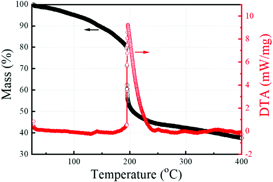 | ||
| Fig. 1 TGA (black symbols) and DTA (red symbols) curves of the dried 0.05 M solution. | ||
The films were prepared at 350 °C, which was found to be a good compromise between the conductivity values and temperature-compatibility with sensitive substrates. GIXRD patterns of the films prepared from the solutions with different concentrations are shown in Fig. 2a. Sharp peaks are presented in all the patterns at 21.6°, 30.7°, 35.6° and 51.6°, corresponding to (211), (222), (400) and (440) planes, respectively, of the body-centered cubic In2O3.28 The peaks become sharper and more intense with decreasing solution concentration (see inset of Fig. 2a).
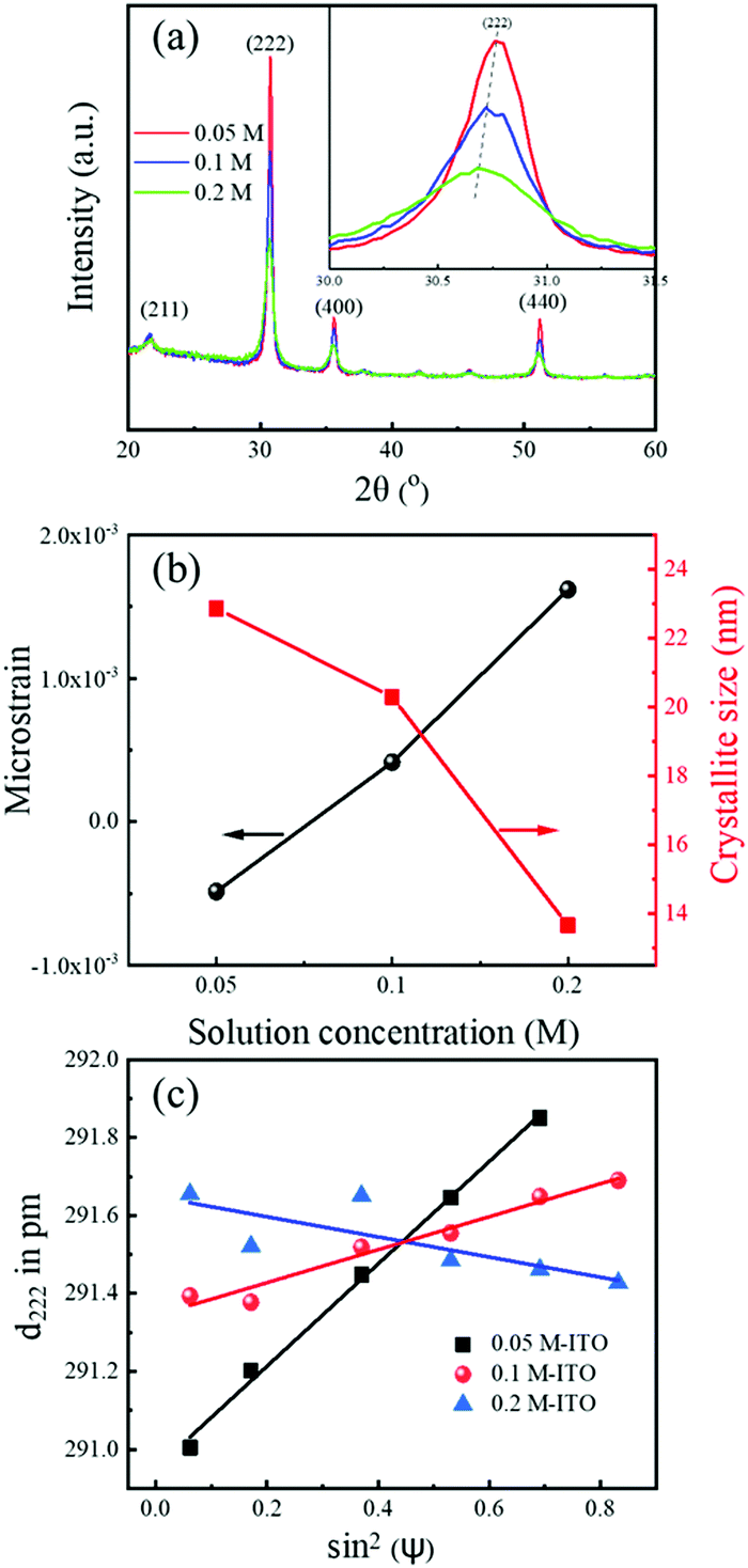 | ||
| Fig. 2 (a) GIXRD patterns of ∼50 nm-thick ITO films prepared from 0.05, 0.1 and 0.2 M solutions by spinning at 2000 rpm and annealing at 350 °C. The peaks of the cubic bixbyite structure are denoted with their Miller indices.28 (b) Microstrain ε and crystallite size D extracted from GIXRD patterns using the W–H method. (c) Lattice spacing d222 as a function of sin2ψ obtained by performing ψ-dependent GIXRD measurements. Their values were corrected due to GIXRD geometry, as described in the ESI.† In (a) the inset shows magnified view around (222) peak. In (b) lines between the experimental points are guides to the eyes. In (c) lines are linear fits. Note that in the case of the 0.2 M sample the quality of linear fit in (c) is not enough to reliably deduce the stress value. | ||
Using the Williamson–Hall method (W–H), crystallite size D (i.e. size of coherently diffracting domains) and microstrain ε (i.e. distribution of interplanar spacing arising from strain fields caused by lattice defects)29 were calculated. Details of the analysis are shown in the ESI.† The extracted D values are 13.6, 20.3, and 22.9 nm, while ε values are 1.6 × 10⁻³, 4.2 × 10⁻⁴ and −4.8 × 10⁻⁴ for respective solution concentrations of 0.2, 0.1 and 0.05 M, as shown in Fig. 2b. This indicates significant growth of crystallites and improved crystallinity with decreasing solution concentration. In addition, roughness evaluated from AFM images in Fig. S2 (ESI†) is lower than 0.5 nm in all the films, illustrating rather smooth surface of the as-fabricated films.
Tilt-angle-dependent GIXRD measurements were performed in order to evaluate residual biaxial stress in the ITO samples (see the ESI† for further information on measurements and analysis).30,31 Lattice spacing d222 is shown as a function of sin2ψ in Fig. 2c. The slope of the lines is directly related to the magnitude of stress. It remarkably drops from 390 MPa (tensile) to zero (within the measurement accuracy) as solution concentration increases from 0.05 to 0.2 M, which is also reflected in the (222) peak shift in Fig. S4 (ESI†). The stress drop is attributed to porosity that increases with concentration, as discussed later.32
The XRR measurements are displayed in Fig. 3a. Oscillations are present in all three curves and their periodicity does not change, indicating similar thicknesses of the films (∼50 nm), as obtained from the fits. Since the films from 0.05, 0.1 and 0.2 M solutions were prepared by 15, 8 and 4 depositions, respectively, this indicates that individual layers are 3, 6 and 12 nm-thick.
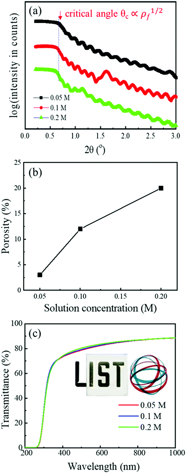 | ||
| Fig. 3 (a) XRR patterns of ITO thin films prepared from solutions with different concentrations. (b) Extracted porosity of the films as a function of solution concentration. (c) Optical transmittance of the films. In (b) lines between the experimental points are guides to the eyes. In (c) the inset shows visual appearance of ITO-coated glass. | ||
Another feature observed in XRR is that the critical angle (defined as the angle at which intensity decreases to half of its maximum value) shifts to higher values with decreasing concentration of the solutions. Density ρf, which is proportional to the critical angle, was determined to be as high as 7.0 g cm−3 for the low-concentration film. This is 97% of the theoretical density (TD), i.e. 7.2 g cm−3 for bulk ITO with the ratio of In:Sn = 9:1.33 On the other hand, the density of the high-concentration film is as low as 5.8 g cm−3. Porosity P was calculated as P = 1 − ρf/ρb, where ρb is bulk TD. It reaches 3% in the film prepared from the 0.05 M solution. Its remarkable dependence on the solution concentration is plotted in Fig. 3b.
Optical transmittance of the films is shown in Fig. 3c. Interestingly, the concentration of the solutions does not have a major impact on the optical properties. In all cases, the value of transmittance at 550 nm is 81%. The visual appearance of the film on glass is shown in the inset of Fig. 3c.
We investigated further the influence of the thickness of individual layers on porosity and have prepared films from the 0.1 M solutions by spinning at different speeds (1800–3000 rpm). The results of all the experiments are collected in Fig. 4a and they indicate that porosity is governed by the thickness of the individual deposited layer, i.e., it is not dependent on the way the thickness is achieved (either by controlling solution concentration or spinning speed). The conductivity σf of the films, calculated from eqn (1) using the thickness obtained from XRR, is shown as a function of porosity in Fig. 4b. It decreases from 620 S cm−1 to 220 S cm−1 for porosities of 3% and 20%, respectively.
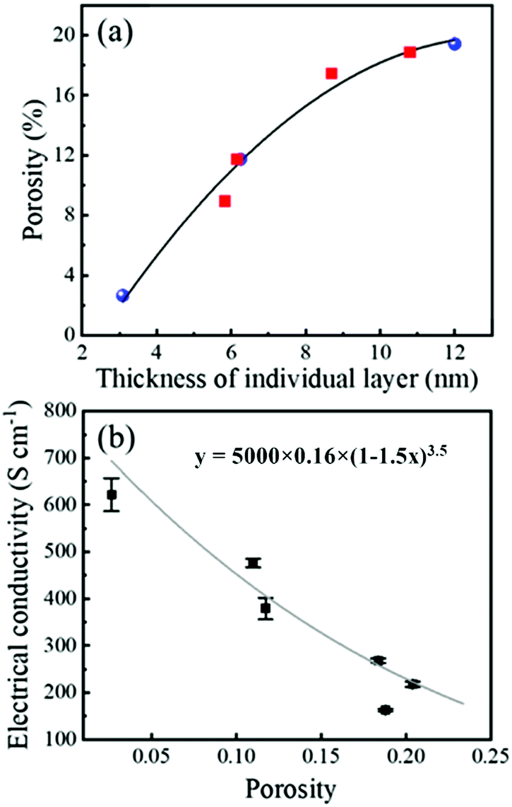 | ||
| Fig. 4 (a) Relationship between film porosity and thickness of individual layers in 40–70 nm thick films. Blue symbols are the values obtained from the films prepared by spinning solutions with different concentrations at 2000 rpm, while red symbols are the values obtained from the films prepared from 0.1 M solution by spinning between 1800 and 3000 rpm. The black line is a guide to the eyes. (b) Electrical conductivity σ of the films as a function of porosity. Symbols are experimental data, grey line is a fit to eqn (2) with a, σb, b, and c parameters of 0.16, 5000, 1.5 and 3.5, respectively. | ||
We employed an empirical mathematical model, commonly used in metal foams:34
| σf = a(1 − bP)cσb, | (2) |
In Fig. 5a, the conductivity value of 620 S cm−1, obtained in the 50 nm-thick 0.05 M-ITO film, is compared to the recent report of Wang et al.,26 in which they used similar solution chemistry and the same annealing temperature (350 °C). The value reported here is more than three times higher compared to their sprayed films and almost 100 times higher compared to their spin coated films (120 nm-thick). Conductivity reported in this work is higher than most of the low-temperature (<400 °C) processed ITO thin films reported so far,11,26,36–38 as shown in Fig. 5b. To boost its value further, temperatures above 500 °C are typically required.24,39–48 Another approach has recently been suggested by Ban et al.,49 who combined photo-annealing and combustion synthesis to supply both the photonic energy and self-generated thermal energy instead of thermal energy at high temperature. This approach increased ITO conductivity up to 1600 S cm−1. Note that our ITO is conductive enough for solar cells, thin film transistors and light emitted diodes,2,10,43 which can avoid the use of complex annealing technologies or annealing in H2, thus reducing the processing cost in the fabrication of these devices.
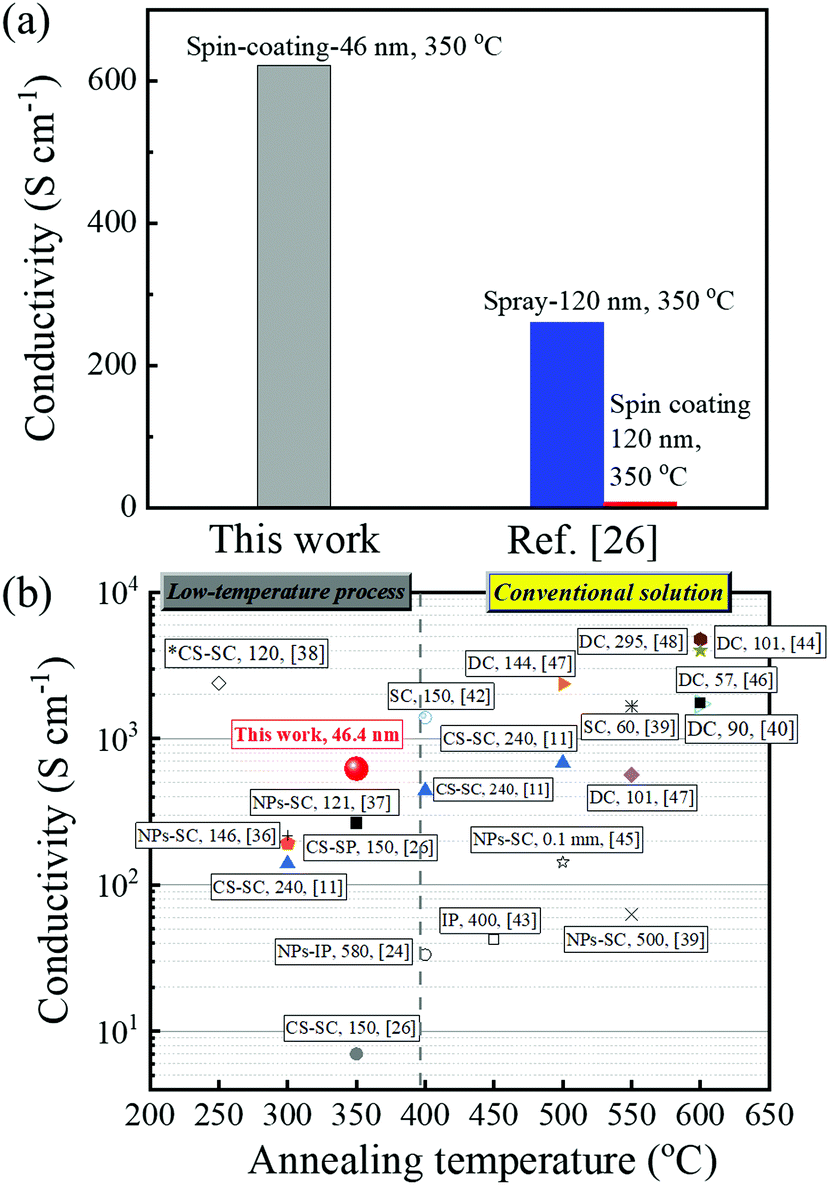 | ||
| Fig. 5 (a) Comparison of the conductivity values obtained in this work and the report of Wang et al.26 in which a similar solution chemistry was used. (b) A summary of conductivity values recently reported on solution-processed ITO films, deposited using different methods (SC: spin coating; SP: spray; NPs: nanoparticles; CS: combustion synthesis; DC: dip coating, IP: inkjet printing; *: directly annealed at a reducing atmosphere). Most of the films were annealed in the air and then in a reducing atmosphere, except the one marked with *, which was prepared by direct annealing in a reducing atmosphere. The techniques, thicknesses (nm) and reference numbers are presented in rectangular boxes. | ||
The obvious question that arises is what is the mechanism behind the improved microstructure and electrical conductivity of the films prepared by multilayer-deposition of very thin layers. Fig. 6a shows the chemical reaction of the transformation from the nitrate precursor to the final In2O3 in the case of the combustion process that is expected to be similar also in the case of ITO films. A large amount of gaseous products is released (21 mol per 1 mol of In2O3), i.e. much more than in the conventional route (7.5 and 3 mols per 1 mol of In2O3, in the case of nitrate and chloride precursors, respectively). The effect of released gas on the microstructure of the films depends strongly on their specific surface area, which is inversely proportional to the film thickness. This is expected to have a two-fold influence on the microstructural evolution in the multilayered thin films, as schematically shown in Fig. 6b. Firstly, it enables a more efficient removal of the gaseous products from the inner part of the films in the case of thinner layers, resulting in lower porosity (see Fig. 3b). Secondly, a faster removal of the gas will result in increased kinetics of the combustion reaction50 and an increased amount of released heat in a shorter amount of time, which results in larger grain size and improved crystallinity of the final films (see Fig. 2b). The enlarged crystallite size in 0.05 M-ITO films reduces the number of grain boundaries, which are considered as one of the most critical phenomena hindering electron transport. Besides, the decrease of crystal defects reflected in the improvement of microstrain also enhances electron transport and therefore improves conductivity. Note that it is also further increased by the post-annealing in vacuum as the number of oxygen vacancies, playing the role of electron donors in n-type metal–oxides, increases.
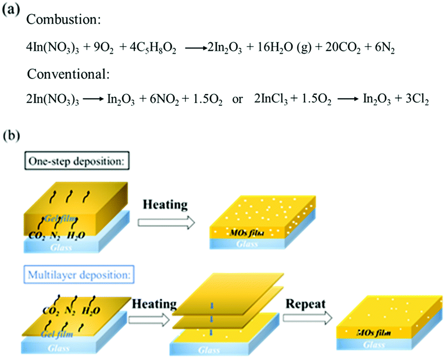 | ||
| Fig. 6 (a) Chemical formulas of combustion and classical (nitrate- and chloride-routes) reactions to obtain In2O3 thin films. (b) Schematic diagram of the influence of gaseous products on porosity in one-step- and multilayer-deposited films. | ||
Conclusion
In this study, we prepared at low-temperature (350 °C) ITO films through combustion synthesis and multilayer deposition. Porosity and crystallinity of the films can be effectively improved by downscaling the thickness of individual layers, which has been observed with X-ray-based techniques. This is attributed to increased surface-to-volume ratio and enhanced release of gaseous products. A strong increase of biaxial stress has also been observed. The microstructural improvements lead to an enhanced electrical conductivity of 620 S cm−1, while optical transmittance remains unchanged, i.e., 81% at 550 nm. An empirical equation shows the strong negative influence of porosity on the electrical conductivity of solution-processed transparent oxide thin films. These results pave the way to a facile approach for the fabrication of high-quality transparent metal–oxide thin films at low temperatures, which is important for future transparent and flexible electronics.Conflicts of interest
There are no conflicts to declare.Acknowledgements
Luxembourg National Research Fund (FNR) is acknowledged for the financial support (PRIDE17/12246511/PACE). Régis Vaudemont and Benoît Marcolini are acknowledged for performing thermal analysis.Notes and references
- F. Y. Wang, L. F. Song, H. C. Zhang, Y. Meng, L. Q. Luo, Y. Xi, L. Liu, N. Zhang, Z. X. Yang, J. Tang, F. K. Shan and J. C. Ho, Adv. Electron. Mater., 2018, 4, 1700336 CrossRef.
- K. Nomura, H. Ohta, A. Takagi, T. Kamiya, M. Hirano and H. Hosono, Nature, 2004, 432, 488–492 CrossRef CAS PubMed.
- L. Wang, M.-H. Yoon, G. Lu, Y. Yang, A. Facchetti and T. J. Marks, Nat. Mater., 2006, 5, 893–900 CrossRef CAS PubMed.
- L. Song, L. Luo, X. Li, D. Liu, N. Han, L. Liu, Y. Qin, J. C. Ho and F. Wang, Adv. Electron. Mater., 2019, 5, 1800707 CrossRef.
- H. Zhang, Y. Meng, L. Song, L. Luo, Y. Qin, N. Han, Z. Yang, L. Liu, J. C. Ho and F. Y. Wang, Nano Res., 2018, 11, 1227–1237 CrossRef CAS.
- X. Zhu, Y. Li, H. Zhang, L. Song, H. Zu, Y. Qin, L. Liu, Y. Li and F. Wang, J. Alloys Compd., 2020, 830, 154578 CrossRef CAS.
- C. Brox-Nilsen, J. Jin, Y. Luo, P. Bao and A. M. Song, IEEE Trans. Electron Devices, 2013, 60, 3424–3429 CAS.
- P. Carcia, R. McLean, M. Reilly and G. Nunes Jr, Appl. Phys. Lett., 2003, 82, 1117–1119 CrossRef CAS.
- A. Liu, H. Zhu, Z. Guo, Y. Meng, G. Liu, E. Fortunato, R. Martins and F. Shan, Adv. Mater., 2017, 29, 1701599 CrossRef PubMed.
- X. Yu, J. Smith, N. Zhou, L. Zeng, P. Guo, Y. Xia, A. Alvarez, S. Aghion, H. Lin and J. Yu, Proc. Natl. Acad. Sci. U. S. A., 2015, 112, 3217–3222 CrossRef CAS PubMed.
- M.-G. Kim, M. G. Kanatzidis, A. Facchetti and T. J. Marks, Nat. Mater., 2011, 10, 382–388 CrossRef CAS PubMed.
- S. Wu, Q. Zhang, Z. Chen, L. Mo, S. Shao and Z. Cui, J. Mater. Chem. C, 2017, 5, 7495–7503 RSC.
- Y. Li, L. Lan, S. Sun, Z. Lin, P. Gao, W. Song, E. Song, P. Zhang and J. Peng, ACS Appl. Mater. Interfaces, 2017, 9, 8194–8200 CrossRef CAS PubMed.
- S.-Y. Kim, K. Kim, Y. Hwang, J. Park, J. Jang, Y. Nam, Y. Kang, M. Kim, H. Park and Z. Lee, Nanoscale, 2016, 8, 17113–17121 RSC.
- J. W. Hennek, J. Smith, A. Yan, M.-G. Kim, W. Zhao, V. P. Dravid, A. Facchetti and T. J. Marks, J. Am. Chem. Soc., 2013, 135, 10729–10741 CrossRef CAS PubMed.
- A. Liu, Z. Guo, G. Liu, C. Zhu, H. Zhu, B. Shin, E. Fortunato, R. Martins and F. Shan, Adv. Electron. Mater., 2017, 3, 1600513 CrossRef.
- X. Yu, T. J. Marks and A. Facchetti, Nat. Mater., 2016, 15, 383–396 CrossRef CAS PubMed.
- Y.-H. Kim, J.-S. Heo, T.-H. Kim, S. Park, M.-H. Yoon, J. Kim, M. S. Oh, G.-R. Yi, Y.-Y. Noh and S. K. Park, Nature, 2012, 489, 128–132 CrossRef CAS PubMed.
- S.-Y. Han, G. S. Herman and C.-H. Chang, J. Am. Chem. Soc., 2011, 133, 5166–5169 CrossRef CAS PubMed.
- Y. S. Rim, W. H. Jeong, D. L. Kim, H. S. Lim, K. M. Kim and H. J. Kim, J. Mater. Chem., 2012, 22, 12491–12497 RSC.
- K. Banger, Y. Yamashita, K. Mori, R. Peterson, T. Leedham, J. Rickard and H. Sirringhaus, Nat. Mater., 2011, 10, 45–50 CrossRef CAS PubMed.
- S.-J. Hong, Y.-H. Kim and J.-I. Han, IEEE Trans. Nanotechnol., 2008, 7, 172–176 Search PubMed.
- H. Zhang, J. Cheng, F. Lin, H. He, J. Mao, K. S. Wong, A. K.-Y. Jen and W. C. Choy, ACS Nano, 2016, 10, 1503–1511 CrossRef CAS PubMed.
- M.-S. Hwang, B.-Y. Jeong, J. Moon, S.-K. Chun and J. Kim, Mater. Sci. Eng., B, 2011, 176, 1128–1131 CrossRef CAS.
- B. Cui, L. Zeng, D. Keane, M. J. Bedzyk, D. B. Buchholz, R. P. Chang, X. Yu, J. Smith, T. J. Marks and Y. Xia, J. Phys. Chem. C, 2016, 120, 7467–7475 CrossRef CAS.
- B. Wang, X. Yu, P. Guo, W. Huang, L. Zeng, N. Zhou, L. Chi, M. J. Bedzyk, R. P. Chang and T. J. Marks, Adv. Electron. Mater., 2016, 2, 1500427 CrossRef.
- M. Björck and G. Andersson, J. Appl. Crystallogr., 2007, 40, 1174 CrossRef.
- ICDD database PDF4+ v4.19, 2019.
- A. Khorsand, W. H. Abd, M. E. Abrishami and R. Yousefi, Solid State Sci., 2011, 13, 251–256 CrossRef.
- T. Dümmer, B. Eigenmann and D. Löhe, Mater. Sci. Forum, 2000, 321–324, 81–86 Search PubMed.
- T. Schenk, C. M. Fancher, M. H. Park, C. Richter, C. Künneth, A. Kersch, J. L. Jones, T. Mikolajick and U. Schroeder, Adv. Electron. Mater., 2019, 12, 1900303 CrossRef.
- A. Mehner, H. Klumper-Westkamp, F. Hoffmann and P. Mayr, Thin Solid Films, 1997, 308–309, 363–368 CrossRef CAS.
- H. Wulff, M. Quaas and H. Steffen, Thin Solid Films, 1999, 355–356, 395–400 CrossRef CAS.
- F. Cuevas, J. Montes, J. Cintas and P. Urban, J. Porous Mater., 2009, 16, 675 CrossRef CAS.
- M. Al-Kuhaili, J. Mater. Sci.: Mater. Electron., 2020, 1–12 Search PubMed.
- J. Lee, S. Lee, G. Li, M. A. Petruska, D. C. Paine and S. Sun, J. Am. Chem. Soc., 2012, 134, 13410–13414 CrossRef CAS PubMed.
- T. O. L. Sunde, E. Garskaite, B. Otter, H. E. Fossheim, R. Sæterli, R. Holmestad, M.-A. Einarsrud and T. Grande, J. Mater. Chem., 2012, 22, 15740–15749 RSC.
- P. T. Tue, S. Inoue, Y. Takamura and T. Shimoda, Appl. Phys. A: Mater. Sci. Process., 2016, 122, 623 CrossRef.
- N. Al-Dahoudi and M. A. Aegerter, Thin Solid Films, 2006, 502, 193–197 CrossRef CAS.
- S. Seki, Y. Sawada and T. Nishide, Thin Solid Films, 2001, 388, 22–26 CrossRef CAS.
- R. Ota, S. Seki, M. Ogawa, T. Nishide, A. Shida, M. Ide and Y. Sawada, Thin Solid Films, 2002, 411, 42–45 CrossRef CAS.
- Z. Chen, W. Li, R. Li, Y. Zhang, G. Xu and H. Cheng, Langmuir, 2013, 29, 13836–13842 CrossRef CAS PubMed.
- N. Xia and R. Gerhardt, Advanced Manufacturing, Electronics and Microsystems—TechConnect Brief, 2016, pp. 163–167 Search PubMed.
- R. Bel Hadj Tahar, T. Ban, Y. Ohya and Y. Takahashi, J. Appl. Phys., 1998, 83, 2139–2141 CrossRef CAS.
- S.-J. Hong and J.-I. Curr, Appl. Phys., 2006, 6, 206–210 Search PubMed.
- R. Ota, S. Seki, Y. Sawada, M. Ogawa, T. Nishide, A. Shida and M. Ide, Surf. Coat. Technol., 2003, 169, 521–524 CrossRef.
- T. Maruyama and A. Kojima, Jpn. J. Appl. Phys., 1988, 27, L1829 CrossRef CAS.
- S. Seki, Y. Sawada, M. Ogawa, M. Yamamoto, Y. Kagota, A. Shida and M. Ide, Surf. Coat. Technol., 2003, 169, 525–527 CrossRef.
- S. G. Ban, K. T. Kim, B. D. Choi, J. W. Jo, Y. H. Kim, A. Facchetti, M. G. Kim and S. K. Park, ACS Appl. Mater. Interfaces, 2017, 9(31), 26191–26200 CrossRef CAS PubMed.
- E. A. Cochran, D.-H. Park, M. G. Kast, L. J. Enman, C. K. Perkins, R. H. Mansergh, D. A. Keszler, D. W. Johnson and S. W. Boettcher, Chem. Mater., 2017, 29, 9480–9488 CrossRef CAS.
Footnote |
| † Electronic supplementary information (ESI) available. See DOI: 10.1039/d0ma00872a |
| This journal is © The Royal Society of Chemistry 2021 |