 Open Access Article
Creative Commons Attribution 3.0 Unported Licence
A new crystal family of GaNGeC quaternary compounds including direct band gap semiconductors and metals†
Ping
Lou
 *ab and
Jin Yong
Lee
 *a
*a
aDepartment of Chemistry, Sungkyunkwan University, Suwon 16419, Korea. E-mail: jinylee@skku.edu
bDepartment of Physics, Anhui University, Hefei 230039, Anhui, China. E-mail: loup@ahu.edu.cn
First published on 30th March 2021
Abstract
Predicting the crystal structures of novel quaternary compounds can be challenging, as there are only a few stable structures among numerous possible ones. Using a recently developed particle swarm optimization-based crystal structure prediction method and the first-principles calculation method, we discover a new crystal family of quaternary GaNGeC compounds, including six direct band gap semiconductors (denoted as S-1, S-2, S-3, S-4, S-5 and S-6) and two metals (denoted as S-7 and S-8); these compounds can potentially be employed in optoelectronic and energy applications. S-1, S-2, S-3, S-4, S-5 and S-6 exhibit high optical absorption coefficients in the visible region. Moreover, S-1, S-2, S-3, S-4 and S-5 possess band edge positions of the valence band maximum and conduction band minimum that are suitable for photocatalytic overall water splitting in the visible region.
1 Introduction
Light-to-electricity conversion has been extensively applied in solar cells, photocatalysis, optoelectronic devices, chemical and biological sensing, and optical communication and imaging processes; in addition, it has continually been the focus of scientific and technological studies. For example, in the photocatalytic water splitting process, sunlight illuminates semiconductors, and photons generate pairs of electrons and holes.1,2,3 The excited holes participate in an oxidation reaction to generate O2, and the excited electrons participate in a hydrogen reduction reaction to generate H2. To achieve such a photocatalytic overall water-splitting process, the semiconductor must possess suitable band edge positions of the valence band maximum (VBM) and conduction band minimum (CBM). In other words, for such a photocatalytic overall water-splitting process to be thermodynamically favourable, the position of the VBM must be lower than the oxidation potential of O2/H2O and the position of the CBM must be higher than the reduction potential of H+/H2.2In short, the research and development of new semiconductor materials with suitable energy band gaps are the cornerstone for solar cells, photocatalysis, optoelectronic devices, chemical and biological sensing, and optical communication and imaging applications. However, the bottlenecks of new material research and development are the long development cycle and high cost. In recent decades, the combination of structure search algorithms and first-principles calculations has helped in predicting the crystal structure; this substantially reduces the required investments, in addition to significantly shortening the development cycle of new materials.4 For example, CALYPSO (crystal structure analysis based on the particle swarm optimization)5,6 has been widely applied to predict the structures of various new materials, including super-hard materials, superconducting materials, semiconducting materials and half-metallic materials.7,8,9,10,11 Moreover, the structures of several new materials predicted using CALYPSO have been experimentally confirmed.7,8
On the other hand, recently, gallium nitride (GaN) and germanium carbide (GeC) monolayers and GeC/GaN van der Waals (vdW) heterojunctions have been studied.12 GaN monolayers have been experimentally synthesized.13,14,15,16 Moreover, three-dimensional (3D) GaN has excellent electronic and optical properties, as a typical representative of third-generation semiconductors, and has been widely used in microwave communications, light-emitting diodes and laser diodes in the ultraviolet range. Recently, GaCN and GeCN ternary compounds, such as Ga2(CN2)3 and GeCN2, have been predicted by the calculations from materials project.17 However, so far, there is no research report on GaNGeC quaternary compound. A naturally interesting question is whether GaNGeC quaternary structures exist? If they exist, what electronic and optical properties do they have? Motivated by these issues, we have used CALYPSO to perform GaNGeC quaternary structure search simulations, and calculated the elastic constants, phonon dispersion, binding energy and formation energy of the possible structures. Only eight crystal structures of the GaNGeC quaternary compound are found to be stable. Furthermore, electronic structure calculations show that six of these are direct band gap semiconductors, and the other two are metals.
2 Computation details
2.1 Crystal structure prediction
The search and prediction of crystal structures are carried out via crystal structure analysis based on the particle swarm optimization (CALYPSO) algorithm.5,6 For the GaNGeC system, the molar ratio (Ga![[thin space (1/6-em)]](https://www.rsc.org/images/entities/char_2009.gif) :
:![[thin space (1/6-em)]](https://www.rsc.org/images/entities/char_2009.gif) N
N![[thin space (1/6-em)]](https://www.rsc.org/images/entities/char_2009.gif) :
:![[thin space (1/6-em)]](https://www.rsc.org/images/entities/char_2009.gif) Ge
Ge![[thin space (1/6-em)]](https://www.rsc.org/images/entities/char_2009.gif) :
:![[thin space (1/6-em)]](https://www.rsc.org/images/entities/char_2009.gif) C = 1
C = 1![[thin space (1/6-em)]](https://www.rsc.org/images/entities/char_2009.gif) :
:![[thin space (1/6-em)]](https://www.rsc.org/images/entities/char_2009.gif) 1
1![[thin space (1/6-em)]](https://www.rsc.org/images/entities/char_2009.gif) :
:![[thin space (1/6-em)]](https://www.rsc.org/images/entities/char_2009.gif) 1
1![[thin space (1/6-em)]](https://www.rsc.org/images/entities/char_2009.gif) :
:![[thin space (1/6-em)]](https://www.rsc.org/images/entities/char_2009.gif) 1) is fixed. 30 and 50 were set for the population size and the number of generations. For each generation, 60% of the structure is constructed by the CALYPSO algorithm, and the remaining 40% is randomly generated to prevent premature convergence of the structure prediction. In the structure search process, first principles are used for structural relaxation and total energy calculation. We performed the exploration with 1 to 4 chemical formulas of GaNGeC in the unit cell.
1) is fixed. 30 and 50 were set for the population size and the number of generations. For each generation, 60% of the structure is constructed by the CALYPSO algorithm, and the remaining 40% is randomly generated to prevent premature convergence of the structure prediction. In the structure search process, first principles are used for structural relaxation and total energy calculation. We performed the exploration with 1 to 4 chemical formulas of GaNGeC in the unit cell.
2.2 Analysis of elastic constants and mechanical properties
The analysis of elastic constants and mechanical properties is performed using the ElAM software package.182.3 Phonon dispersions
Calculations regarding phonon dispersions are performed using the Quantum-ESPRESSO code.19 The planewave cutoff was set to 120 Ry with a norm-conserving pseudopotential, and the Brillouin zone (BZ) integration was performed with the 12 × 12 × 12 k-point sampling points, and dynamic matrix integral was chosen to be a 6 × 6 × 6 mesh of q-point.2.4 Calculation details of the electronic band structures, elastic constants and optical spectra
In this study, most calculations pertaining to DFT (the standard density functional theory) and GW (the G0W0 approximation) electronic band structures,12,20,21 elastic constants and GW + BSE optical spectra (calculated using the combination of GW and Bethe Salpeter equation (BSE) method)12,20,21 are performed using the Vienna Ab initio Simulation Package (VASP).22,23 The projector augmented wave pseudo potential,23 plane wave basis set, and Perdew Burke Ernzerhof (PBE) exchange correlation functional,24 including the vdW dispersive corrections25 and spin–orbit coupling (SOC), were applied. In the electronic band structures and elastic constants calculations, Monkhorst Pack k-point meshes with the grid density of 0.03 × 2π Å−1 were applied to achieve a total energy convergence of ≤1 meV per atom. For electronic band structures, the test calculations with the strongly constrained and appropriately normed (SCAN) nonempirical density functional26,27 and HSE06 hybrid functional27,28,29,30 also had been performed. In the GW and GW-BSE calculations, the plane wave cutoff energy, number of bands, Monkhorst–Pack grid, dielectric matrix cutoff and number of conduction bands have been converged carefully to 700 eV, 10 × 10 × 10, 450 eV and 256, respectively.The optical absorption coefficient α(ω) was given as:
 | (1) |
3 Results and discussions
3.1 Crystal structure
Crystal structures of the eight GaNGeC compounds are shown in Fig. 1 based on the decreasing formation energy, denoted as S-1, S-2, S-3, S-4, S-5, S-6, S-7 and S-8. As listed in Table 1 and Table S1 in the ESI,† S-1, S-6 and S-8 are identified as trigonal with the P3m1 space group (No. 156); S-5 and S-7 are also identified as trigonal, but their space group is R3m (No. 160); and S-2, S-3 and S-4 are identified as orthorhombic with the Pmm2 space group (No. 25).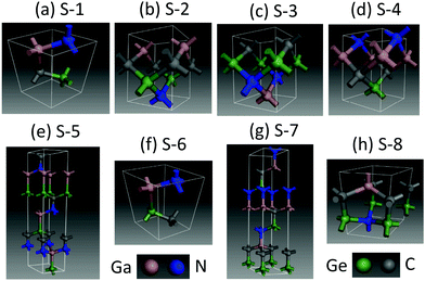 | ||
| Fig. 1 Crystal structures of the eight GaNGeC compounds: (a) S-1, (b) S-2, (c) S-3, (d) S-4, (e) S-5, (f) S-6, (g) S-7 and (h) S-8. | ||
| Space group | a | b | c | α | β | γ | E b | E f | E GWg | E Optg | |
|---|---|---|---|---|---|---|---|---|---|---|---|
| S-1 | P3m1 | 3.242 | 3.242 | 5.321 | 90 | 90 | 120 | −5.940 | −0.398 | 3.06 | 2.86 |
| S-2 | Pmm2 | 3.241 | 3.254 | 4.564 | 90 | 90 | 90 | −5.856 | −0.316 | 1.85 | 1.65 |
| S-3 | Pmm2 | 3.241 | 3.254 | 4.564 | 90 | 90 | 90 | −5.857 | −0.316 | 1.84 | 1.63 |
| S-4 | Pmm2 | 3.241 | 3.254 | 4.564 | 90 | 90 | 90 | −5.857 | −0.316 | 1.85 | 1.65 |
| S-5 | R3m | 5.835 | 5.835 | 5.835 | 32.074 | 32.074 | 32.074 | −5.709 | −0.168 | 1.62 | 1.45 |
| S-6 | P3m1 | 3.209 | 3.209 | 5.568 | 90 | 90 | 120 | −5.681 | −0.140 | 1.21 | 1.04 |
| S-7 | R3m | 5.647 | 5.647 | 5.647 | 33.956 | 33.956 | 33.956 | −5.660 | −0.118 | 0 | 0 |
| S-8 | P3m1 | 3.301 | 3.301 | 5.226 | 90 | 90 | 120 | −5.649 | −0.108 | 0 | 0 |
On the other hand, S-1, S-5, S-6, S-7 and S-8 present a hexagonal layered structure along the c-axis direction as they belong to the hexagonal crystal family. Specifically, S-1, S-5 and S-6 comprise GaN and GeC monolayers with different stacks, whereas S-7 and S-8 comprise GaC and GeN monolayers with different stacks. Recently, GaN and GeC monolayers and GeC/GaN van der Waals (vdW) heterojunctions have been studied.12 Moreover, GaN monolayers have been experimentally synthesized.13,14,15,16 The research of the current paper provides a new way to investigate the GaNGeC system from bulk materials to thin films, the double-layer vdW heterojunction and single-layer.
3.2 Phonon dispersions
Phonon dispersions of the eight crystal structures were analysed to determine their dynamical stability. As shown in Fig. 2, no negative phonon frequencies were found in the entire Brillouin zone (BZ), which indicates the dynamic stability of the eight crystals.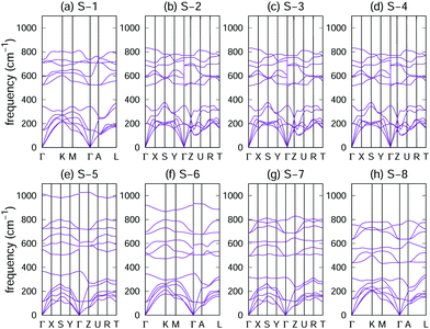 | ||
| Fig. 2 Phonon dispersions of the eight crystal structures of the GaNGeC compound: (a) S-1, (b) S-2, (c) S-3, (d) S-4, (e) S-5, (f) S-6, (g) S-7 and (h) S-8. | ||
3.3 Elastic constants and mechanical properties
To investigate the mechanical stability of the eight crystal structures of the GaNGeC compound, their elastic constants, Cij, were calculated. As listed in Table 2, they satisfy the mechanical stability criteria.18,32 For example, for S-1, S-5, S-6, S-7 and S-8, according to their rhombohedral(I) symmetry, C11 = C22, C13 = C23, C44 = C55 and C66 = (C11 – C12); thus, they have only six independent elastic constants, which satisfy C11 > |C12|, C55 > 0, C132 <
  (C11 + C12) and C142 <
  (C11 – C12). According to the orthorhombic symmetry of S-2, S-3 and S-4, the nine elastic constants are independent and satisfy C11C22C33 + 2C12C13C23 > C11C232 + C22C132 + C33C122, C11 > 0, C11C22 > C122, C44 > 0, C55 > 0 and C66 > 0. Thus, they are mechanically stable.
| C 11 | C 12 | C 13 | C 14 | C 22 | C 23 | C 33 | C 44 | C 55 | C 66 | |
|---|---|---|---|---|---|---|---|---|---|---|
| S-1 | 348.33 | 87.18 | 51.76 | −3.61 | 348.33 | 51.76 | 381.43 | 103.11 | 103.11 | 130.58 |
| S-2 | 394.60 | 38.59 | 126.21 | 0.00 | 369.12 | 130.84 | 273.13 | 168.36 | 166.77 | 85.92 |
| S-3 | 395.86 | 37.46 | 125.41 | 0.00 | 371.00 | 129.74 | 277.88 | 167.36 | 166.89 | 83.55 |
| S-4 | 396.37 | 37.82 | 126.18 | 0.00 | 370.01 | 129.77 | 277.00 | 167.56 | 166.91 | 84.15 |
| S-5 | 355.90 | 78.96 | 38.33 | −22.55 | 355.90 | 38.33 | 429.89 | 76.21 | 76.21 | 138.47 |
| S-6 | 321.51 | 69.76 | 16.12 | 5.49 | 321.51 | 16.12 | 402.86 | 70.17 | 70.17 | 125.87 |
| S-7 | 270.76 | 103.14 | 50.70 | −29.05 | 270.76 | 50.70 | 301.67 | 89.13 | 89.13 | 83.81 |
| S-8 | 270.12 | 108.71 | 60.20 | −5.04 | 270.12 | 60.20 | 329.05 | 85.89 | 85.89 | 80.70 |
Bulk (B), shear (G), and Young's (Y) moduli and hardness (H) and Poisson's ratio ν18,33 were calculated using the elastic constant and are displayed in Fig. 3(a and b). It is known that the larger the elastic modulus, the stronger the chemical bonding. As shown in Fig. 3(a and b), the B, G, Y and H values of S-1, S-2, S-3, S-4, S-5 and S-6 are larger than those of S-7 and S-8; consequently, S-1, S-2, S-3, S-4, S-5 and S-6 have a larger binding energy (Eb) than that of S-7 and S-8 (Table 1). On the other hand, ν measures the stability of a crystal against shear. A smaller value for ν indicates better stability against shear. Materials with ν < 0.26 are brittle and those with ν > 0.26 are considered ductile.34 Although the ν values of S-7 and S-8 (metals) are larger than those of S-1, S-2, S-3, S-4, S-5 and S-6 (semiconductors), they are all brittle in nature.
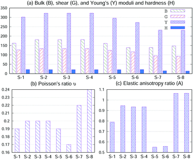 | ||
| Fig. 3 (a) Bulk (B), shear (G), and Young's (Y) moduli and hardness (H), in units of GPa. (b) Poisson's ratio ν. (c) Elastic anisotropy ratio (A). | ||
In materials science, anisotropy refers to the directional dependence of physical properties of materials, and it is considered important in selecting materials for engineering applications. The elastic anisotropy ratio (A), defined by  (also called as the Zener anisotropy ratio),35,36 is calculated to compare the elastic anisotropy exhibited by various materials. For elastic isotropic materials, this ratio is 1. The more the deviation of the ratio from 1, the greater the anisotropy.36 As shown in Fig. 3(c), the ratio A corresponding to S-1, S-2, S-3, S-4, S-5, S-6, S-7 and S-8 deviate 1. Therefore, they are elastic anisotropic materials.
3.4 Binding energy
The structural stability of the eight crystal structures of the GaNGeC compound was assessed based on their binding energies. The binding energy is defined as Eb = (ET − EGa − EGe − EC − EN)/N, where ET is the energy of the crystal structures of the GaNGeC compound. EGa, EGe, EC and EN are the energies of Ga, Ge, C and N atoms, respectively, in their isolated states, while N = 4 is the number of atoms in the crystal structures of the GaNGeC compound. As listed in Table 1, the Eb values of the eight crystal structures were all negative. For example, the Eb value of S-8 was −5.65 eV atom−1, which is sufficiently large to stabilize the structures.3.5 Formation energy
Unlike the binding energy of a compound, the formation energy is related to its specific formation process. Whether the eight crystals of the GaNGeC compound can be formed by Ga, Ge, C and N has been evaluated based on the formation energy. The formation energy is defined by Ef = (ET − EGa − EGe − EC − EN)/N, where ET is the energy of the crystal of the GaNGeC compound and EGa, EGe, EC and EN are the energies of Ga, Ge, C and N atoms, respectively, in their elemental crystal states, instead of their isolated states. As listed in Table 1, the Ef values of the eight crystals of the GaNGeC compound were all negative, indicating that they can be formed by Ga, Ge, C, and N owing to their exothermicities. Moreover, the difference in the formation energies of the eight crystals of the GaNGeC compound was negligible, indicating that they can appear simultaneously during the formation process.3.6 Electronic band structure
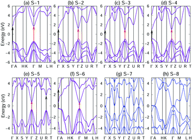
As listed in Table 1, S-1, S-2, S-3, S-4, S-5 and S-6 crystals are semiconductors, whereas S-7 and S-8 are metals. With regard to the semiconductors, the GW band structures12,20,21 are shown, and for metals, the PBE band structures are displayed (Fig. 4). As shown in Fig. 4(a–f), we observe that S-1, S-2, S-3, S-4, S-5 and S-6 are semiconductors having direct band gaps at the Γ-point. The values of the GW band gap of S-1, S-2, S-3, S-4, S-5, and S-6 crystals are 3.06, 1.85, 1.84, 1.85, 1.62 and 1.21 eV, respectively, while the corresponding PBE band gaps are 1.80, 0.85, 0.84, 0.85, 0.57 and 0.23 eV, respectively. Clearly, the PBE calculations severely underestimated the band gaps of the semiconductors. As shown in Fig. S17–S25 in the ESI,† the test calculations with the SCAN26,27 and HSE06 hybrid functionals27,28,29,30 confirmed that S-1, S-2, S-3, S-4, S-5 and S-6 crystals are semiconductors, whereas S-7 and S-8 are metals.The research and development of direct band gap semiconductor materials are crucial for solar applications as the electrons of the indirect band gap semiconductors require photons and phonons for transiting from the valence band to the conduction band. This involves changes in energy (caused by photons) and in nuclei (caused by phonons). However, the transition of electrons from the valence band to the conduction band in a direct band gap semiconductor only requires the photon energy to match the band gap energy without entailing phonons. Therefore, direct band gap semiconductor materials can absorb light more effectively. These direct bandgap semiconductors, covering wide bandgap to narrow forbidden band, provide ideal materials for light-emitting fields, such as light-emitting diodes (LED), laser diodes (LD), light receivers (PIN), and solar cells.
3.7 Band alignment
The photochemical catalysis exhibited by the crystals of the GaNGeC compound has been evaluated using the band arrangement calculated based on empirical formula. The empirical formula used is ECBM/VBM = −X ± 0.5EGWg,37,38 where EGWg is the GW quasiparticle band gap, and X is the Mulliken electronegativity of the material, which is defined as the geometric mean of the Mulliken electronegativity values of the constituent atoms. Based on the Mulliken electronegativity values of N, Ga, Ge and C atoms (7.30, 3.2, 4.6 and 6.27 eV, respectively),37,38X was calculated to be 5.10 eV. As shown in Fig. 5, the energy difference between the VBM and oxidation potential of O2/H2O (ΔEv) and the energy difference between the CBM and reduction potential of H+/H2 (ΔEc) are known as kinetic over potentials, which are necessary to drive the redox reaction. S-1, S-2, S-3, S-4 and S-5 have sufficiently large kinetic over potentials to drive the redox reaction. The band edge positions of the VBM and CBM of S-1, S-2, S-3, S-4 and S-5 meet the requirements of photocatalytic overall water splitting, making them promising candidates for photocatalytic water separation and solar energy conversion.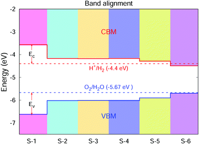 | ||
| Fig. 5 Calculated absolute band edges of S-1, S-2, S-3, S-4, S-5 and S-6, with the vacuum level set to zero. The solid red and blue lines indicate the CBM and VBM band edge positions, respectively. The dotted red and blue lines denote the reduction potential of H+/H2 and the oxidation potential of O2/H2O, respectively.2 | ||
3.8 Optical absorption spectra
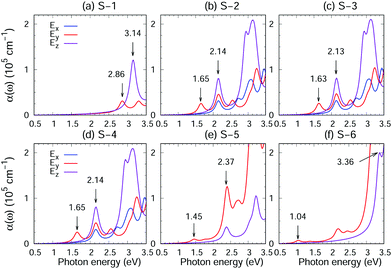
Photocatalyst materials should have satisfactory light absorption capacity. The light absorption capacity of S-1, S-2, S-3, S-4, S-5 and S-6 crystals has been evaluated using the function of light absorption coefficients changing with photon energy, which is calculated using the GW + BS.12,20,21 Moreover, in order to reveal the anisotropy of the optical properties of the material, the optical absorption spectra corresponding to light polarized parallel to the x, y and z directions have been considered, as shown in Fig. 6. S-1, S-2, S-3, S-4, S-5 and S-6 show strong absorption coefficients (approximately 105 cm−1) in the visible range. In addition, the absorption edges of S-1, S-2, S-3, S-4, S-5 and S-6 crystals (optical band gap EOptg) are located in the visible light region and marked in Fig. 6 by the first absorption peak, which has originated from an inter-band transition between the VBM and CBM at the Γ point (see the red arrow Fig. 4(a–f)). According to Table 1 and Fig. 6, the EOptg values of S-1, S-2, S-3, S-4, S-5 and S-6 are 2.86, 1.65, 1.63, 1.65, 1.45 and 1.04 eV, respectively. Moreover, the second absorption peak, for S-1, S-2, S-3 and S-4, has originated from an inter-band transition between the second valence band and the CBM at the Γ point, and for S-5, it has originated from an inter-band transition between the VBM and CBM at the R point. For S-6, the peak has originated from an inter-band transition between the VBM and the second conduction band at the Γ point (black arrow in Fig. 4(a–f)).S-1, S-2, S-3, S-4, S-5 and S-6 exhibit large exciton effects. As listed in Table 1, we have found that the exciton binding energy, the difference between the electronic and optical band gaps (EGWg − EOptg), ranges from 170 to 210 meV. Moreover, as shown in Fig. S11–S16 in the ESI,† the inclusion of an electron hole interaction (red lines) results not only in a significant red shift of the absorption spectrum compared with an absorption spectrum without an electron hole interaction (blue lines) but also in enhanced absorption coefficients.
On the other hand, the absorption spectrum of the light polarized parallel to the x, y and z directions and the intensity of the absorption band clearly demonstrate anisotropy. As shown in Fig. 6(a), (e) and (f), the hexagonal crystal symmetry of S-1, S-5 and S-6 results in in-plane (xy plane) isotropic absorption spectra (displayed using blue and red lines; also see Fig. S11, S15 and S16 in the ESI†) in accordance with the polarization of the incident light. In contrast, as shown in Fig. 6(b–d), the reduced crystal symmetry of S-2, S-3 and S-4 leads to the in-plane anisotropy absorption spectra (blue and red lines), demonstrating potential for the application of these crystals in polarization-sensitive novel optoelectronic devices. For example, in a novel polarization sensitive optoelectronic switching device, the switching behavior of the device depends only on the polarization angle and not on the intensity of the incident light. The polarization sensitivity of the device is based on the inherent polarization anisotropy of spontaneously ordered semiconductor crystals. The electrical output signal of the device can be turned on and off by changing the polarization direction of the incident light.
4 Summary
In summary, we have applied a combination of structure search algorithms and first-principles calculations to predict a new crystal family of quaternary GaNGeC compounds, which includes six direct band gap semiconductors and two metals. The S-1, S-2, S-3, S-4, S-5 and S-6 semiconductors, with direct band gaps of 3.06, 1.85, 1.84, 1.85, 1.62 and 1.21 eV, respectively, exhibit high optical absorption coefficients (∼105 cm−1) in the visible region and have large exciton binding energies (∼200 meV). In addition, S-1, S-2, S-3, S-4 and S-5 show desired band edge positions of the valence band maximum and conduction band minimum that are suitable for photocatalytic overall water splitting in the visible region. This study could open a new avenue for a new family of semiconductors and metals of the GaNGeC systems from bulk materials to thin films, double-layer vdW heterojunctions and single-layer.Conflicts of interest
There are no conflicts to declare.Acknowledgements
This work was supported by the National Research Foundation (NRF) (2019R1A6A1A10073079) funded by the Korean Government (MEST).Notes and references
- X. Wang, K. Maeda, A. Thomas, K. Takanabe, G. Xin, M. J. Carlsson, K. Domen and M. Antonietti, Nat. Mater., 2009, 8, 76–80 CrossRef CAS PubMed.
- V. Chakrapani, J. C. Angus, A. B. Anderson, S. D. Wolter, B. R. Stoner and G. U. Sumanasekera, Science, 2007, 318, 1424–1430 CrossRef CAS PubMed.
- A. Fujishima and K. Honda, Nature, 1972, 238, 37–38 CrossRef CAS PubMed.
- A. R. Oganov, C. J. Pickard, Q. Zhu and R. J. Needs, Nat. Rev. Mater., 2019, 4, 331–348 CrossRef.
- Y. Wang, J. Lv, L. Zhu and Y. Ma, Phys. Rev. B: Condens. Matter Mater. Phys., 2010, 82, 94116 CrossRef.
- Y. Wang, J. Lv, L. Zhu and Y. Ma, Comput. Phys. Commun., 2012, 183, 2063 CrossRef CAS.
- J. Lv, Y. Wang, L. Zhu and Y. Ma, Phys. Rev. Lett., 2011, 106, 15503 CrossRef PubMed.
- H. Liu, I. I. Naumov, R. Hoffmann, N. W. Ashcroft and R. J. Hemley, Proc. Natl. Acad. Sci. U. S. A., 2017, 114, 6990 CrossRef CAS PubMed.
- L. Yan, P. Liu and H. Li, et al. , npj Comput. Mater., 2020, 6, 94 CrossRef CAS.
- T. Yu, Z. Zhao, Y. Sun, A. Bergara, J. Lin, S. Zhan, H. Xu, L. Zhang, G. Yang and Y. Liu, J. Am. Chem. Soc., 2019, 141, 1599–1605 CrossRef CAS PubMed.
- J. Deng, J. Guo and X. Chen, J. Am. Chem. Soc., 2020, 142, 5234–5240 CrossRef CAS PubMed.
- P. Lou and J. Y. Lee, ACS Appl. Mater. Interfaces, 2020, 12, 14289–14297 CrossRef CAS PubMed.
- Z. Y. Al Balushi, K. Wang, R. K. Ghosh, R. A. Vilá, S. M. Eichfeld, J. D. Caldwell, X. Qin, Y.-C. Lin, P. A. DeSario and G. Stone, Nat. Mater., 2016, 15, 1166–1171 CrossRef CAS PubMed.
- B. D. Liu, W. J. Yang, J. Li, X. L. Zhang, P. J. Niu and X. Jiang, Nano Lett., 2017, 17, 3195–3201 CrossRef CAS PubMed.
- C. Sun, M. Yang, T. Wang, Y. Shao, Y. Wu and X. Hao, ACS Appl. Mater. Interfaces, 2017, 9, 26631–26636 CrossRef CAS PubMed.
- T. Imaoka, T. Okada, S. Samukawa and K. Yamamoto, ACS Appl. Mater. Interfaces, 2017, 9, 41629–41633 CrossRef CAS PubMed.
- A. Jain, S. P. Ong, G. Hautier, W. Chen, W. D. Richards, S. Dacek, S. Cholia, D. Gunter, D. Skinner, G. Ceder and K. A. Persson, APL Mater., 2013, 1, 011002 CrossRef.
- A. Marmier, Z. A. D. Lethbridge, R. I. Walton, C. W. Smith, S. C. Parker and K. E. Evans, Comput. Phys. Commun., 2010, 181, 2102–2115 CrossRef CAS.
- P. Giannozzi, O. Andreussi and T. Brumme, et al. , J. Phys.: Condens. Matter, 2017, 29, 465901 CrossRef CAS PubMed.
- P. Lou, RSC Adv., 2017, 7, 52053–52064 RSC.
- J. Deslippe, G. Samsonidze, D. A. Strubbe, M. Jain, M. L. Cohen and S. G. Louie, Comput. Phys. Commun., 2012, 183, 1269–1289 CrossRef CAS.
- P. E. Blöhl, Phys. Rev. B: Condens. Matter Mater. Phys., 1994, 50, 17953–17979 CrossRef PubMed.
- G. Kresse and D. Joubert, Phys. Rev. B: Condens. Matter Mater. Phys., 1999, 59, 1758–1775 CrossRef CAS.
- J. P. Perdew, K. Burke and M. Ernzerhof, Phys. Rev. Lett., 1996, 77, 3865–3868 CrossRef CAS PubMed.
- S. Grimme, J. Comput. Chem., 2014, 27, 1787–1799 CrossRef PubMed.
- J. Sun, A. Ruzsinszky and J. Perdew, Phys. Rev. Lett., 2015, 115, 036402 CrossRef PubMed.
- P. Lou and J. Y. Lee, J. Chem. Phys., 2019, 150, 184307 CrossRef PubMed.
- A. V. Krukau, O. A. Vydrov, A. F. Izmaylov and G. E. Scuseria, J. Chem. Phys., 2006, 125, 224106 CrossRef PubMed.
- C. Zhang, Y. Jiao, T. He, S. Bottle, T. Frauenheim and A. Du, J. Phys. Chem. Lett., 2018, 9, 858–862 CrossRef CAS PubMed.
- P. Lou and J. Y. Lee, J. Phys. Chem. C, 2019, 123, 16994–17001 CrossRef CAS.
- X. Huang, T. R. Paudel, S. Dong and E. Y. Tsymbal, Phys. Rev. B: Condens. Matter Mater. Phys., 2015, 92, 125201 CrossRef.
- F. Mouhat and F. X. Coudert, Phys. Rev. B: Condens. Matter Mater. Phys., 2014, 90, 224104 CrossRef.
- R. Hill, Proc. Phys. Soc., London, Sect. A, 1952, 65, 349–354 CrossRef.
- G. N. Greaves, A. L. Greer, R. S. Lakes and T. Rouxel, Nat. Mater., 2011, 10, 823–837 CrossRef CAS PubMed.
- C. Zener, Phys. Rev., 1947, 71, 846–851 CrossRef CAS.
- Z. A. D. Lethbridge, R. I. Walton, A. S. H. Marmier, C. Smith and K. E. Evans, Acta Mater., 2010, 58, 6444–6451 CrossRef CAS.
- M. A. Butler and D. S. Ginley, J. Electrochem. Soc., 1978, 125, 228–232 CrossRef CAS.
- R. G. Pearson, J. Org. Chem., 1989, 54, 1423–1430 CrossRef CAS.
Footnote |
| † Electronic supplementary information (ESI) available: Fig. S1 shows the total energy per atom as a function of volume per atom. Fig. S2 shows the pressure as a function of volume per atom. Table S1 shows the fractional coordinates of the atom in the primitive cell. Fig. S3–S10 show the atom-resolved projected phonon dispersions. Fig. S11–S16 show the optical absorption coefficient (α(ω)). Fig. S17–S25 show PBE, SCAN, and HSE06 band structures. See DOI: 10.1039/d0ma00844c |
| This journal is © The Royal Society of Chemistry 2021 |

