
 Open Access Article
 This Open Access Article is licensed under a Creative Commons Attribution-Non Commercial 3.0 Unported Licence
Electronic and protonic transport in bio-sourced materials: a new perspective on semiconductivity
Manuel
Reali
 *a,
Pooja
Saini
b and
Clara
Santato
*a
*a,
Pooja
Saini
b and
Clara
Santato
*a
aDepartment of Engineering Physics, Polytechnique Montreal, Montreal, H3C 3A7, Canada. E-mail: clara.santato@polymtl.ca
bDepartment of Physics and Astrophysics, University of Delhi, 110007, New Delhi, India
First published on 26th October 2020
Abstract
Over the last few decades, the terrific development in the field of consumer electronics, paralleled by wider access to technology, short device lifetime and replacement cycles, has generated an unsustainable amount of waste of electrical and electronic equipment. Accumulation of e-waste is posing serious environmental and health concerns for the present and future generations. Abundant, bio-sourced, biocompatible, solution-processable organic materials are promising for promoting the development of low eco- and human-toxic electronic technologies. Therefore, unraveling the structure-to-property relationships in bio-sourced materials is paramount. The study of the charge carrier transport properties of bio-sourced materials is challenging. The presence of ions, and among them protons, in these systems profoundly affects the local molecular environment and, in turn, their charge carrier transport properties. In this context, the question whether the classical concept of semiconductivity developed for inorganic materials applies to protonic as well as mixed protonic–electronic counterparts is a matter of debate. In this review, we shed light on the elusive concept of semiconductivity for nature-inspired materials and provide new perspectives on protonic transport on the definition of bio-sourced semiconductors.
1. Introduction
We are living in an era of tremendous technological achievements. The field of electronics is progressing at a terrific pace to a point where our lives are becoming more and more dependent on it. Despite that we undoubtedly benefit from electronic technologies and devices, such a tremendous boom poses environmental and health concerns. Quoting SONY's founding chairman A. Morita, “we are moving from consumer to consumable electronics”: replacement cycles and lifetime of electronics are becoming shorter and shorter.1,2 According to the Global e-Waste Monitor 2020, 53.6 Mt of e-Waste were produced worldwide in 2019 and this amount is expected to reach 74.7 Mt by 2030.3 A global effort is now in place for achieving a paradigm shift from linear to circular electronics, focusing on durability, reuse, refurbishment and advanced recycling.4 The development of Green (Sustainable) Organic Electronics, based on the use of abundant bio-sourced (extracted from biomass and/or agriculture-waste feedstocks), solution-processed materials, potentially compostable, featuring suitable charge carrier transport properties is a viable route to alleviate the footprint of electronics.5,6In 2000 A. Heeger, A. MacDiarmid, and H. Shirakawa were awarded the Nobel Prize in Chemistry for their discovery that the electrical conductivity of conjugated materials (i.e. materials featuring single–double carbon bonds) can increase by several orders of magnitude via chemical doping.
Since then, bio-sourced or bio-inspired materials have been applied in devices such as organic field-effect transistors,7,8 (e.g. indigo, epindolidione, quinacridone, and tyrian-purple), organic solar cells,9 light-emitting diodes,10,11 phototransistors (e.g. eumelanin),12 organic sensors,5 p–n ionic junctions (i.e. chitosan)13 and many others.14–16 Organic electronics are a promising complement of Silicon (Si) technologies for printable, stretchable and flexible applications.17
Bio-sourced materials are generally wet, that is they can contain protons and mobile ions. In bio-sourced materials, the nature of current can therefore be ionic or mixed ionic–electronic, unlike their inorganic counterparts wherein electronic transport (electrons and holes) prevails.18–21 The presence of ionic species modifies the structural environment of bio-sourced materials (e.g. by generating electronic traps and local dipole moments and/or by changing the dielectric constant) and impacts their mesoscopic properties.
The question whether the models of transport physics developed for inorganic materials apply to bio-sourced ones is evergreen. Given the classical definition of inorganic semiconductors, based on exclusive electronic transport, several questions can be raised: what is the impact of protonic transport in defining the semiconducting properties of bio-sourced, nature-inspired materials? What are the factors that define bio-sourced materials as semiconductors? Does the nature of the predominant charge carrier (electrons/holes vs protons/proton-holes) determine whether a bio-sourced material is a semiconductor or not? Unravelling the mesoscopic properties of bio-sourced materials is a burning need to exploit their full technological potential.
In this review, we tentatively try to answer these questions. We first provide the fundamentals of electronic and protonic transport mechanisms in bio-sourced materials, including the Mott–Davis (MD) amorphous semiconductor model22 and the quantum model of the Grotthus mechanism,23 which leads to the protonic semiconductor model. We then discuss the examples of bio-sourced devices (i.e. protonic p–n junctions, field-effect transistors and light-emitting diodes) whose working principles can be described by using the protonic semiconductor model. We conclude with a case study on the biopigment eumelanin, which for decades has been considered as a semiconductor.24,25 Our analysis brings to light novel perspectives on semiconductivity and calls for a new, holistic definition of bio-sourced semiconductors.
2. Electronic transport in bio-sourced materials
Herein, we present the introductory aspects of band theory for ordered (crystalline) and disordered (amorphous) materials that are fundamental, for a broad readership, to understand the transport physics of bio-sourced materials. To this aim, we briefly present an overview of the band theory of electrical conduction for conventional crystalline solids (Section 2.1) and then its modification for amorphous materials (Section 2.2).The charge carrier transport properties of any material can be described by using the basic conductivity (σ) equation:
| σ = nqμ | (1) |
Detailed analysis of band theory and its extension to amorphous materials is out of scope in this review. For the literature regarding these topics, we invite readers to refer to 18–21.
2.1 Band theory of electronic transport
The properties of electrons in crystalline solids are explained by using band theory. In crystalline solids (inorganic and organic) the structure is composed of units (e.g. atoms, ions, and molecules) arranged in periodic planes of arrays (Bravais lattice). This periodicity is responsible for highly ordered structures and profoundly impacts the foundations of band transport theories.18 The energy levels of an electron are determined considering a steady state single-electron Hamiltonian with the periodicity of the underlying lattice. Indeed, the electron interacts with the lattice units through periodic potential wells. In this framework, the long-range order enables extended delocalization of the electronic wavefunction, and the motion of electrons is described by Bloch waves.Delocalization of electronic charge carriers generates energy bands, namely the valence band (VB) and the conduction band (CB), for the occupancy state of holes and electrons, respectively. The states are extended within the band i.e. the wavefunction occupies the entire volume. The energy difference between the top of the VB (EV) and the bottom of the CB (EC) defines the crystalline band gap region (EG) where no electronic states are found. In metals, the Fermi energy level (εF) lies in between one or more filled bands (e.g. there is no energy gap) and there are already available charge carriers for conduction at any temperature (Fig. 1A). In both semiconductors and insulators, the Fermi energy level εF lies between EV and EC. The value of EG distinguishes semiconductors (EG ∼ 1 to 3 eV, Fig. 1B) from insulators (EG greater than 3 eV, Fig. 1C). In semiconductors and insulators, electronic conduction arises from the excitation of an electron from the VB to the CB by providing the electron with an energy greater than EG; for every electron in the CB a hole (electron counterpart) is left in the VB.
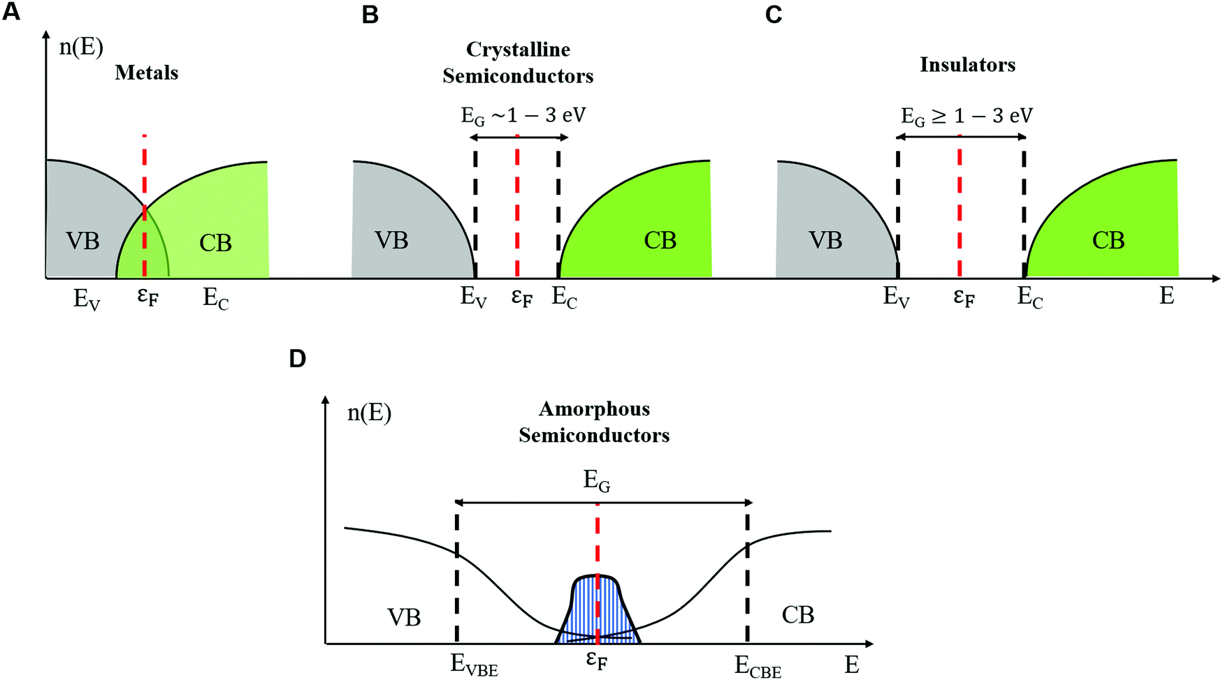 | ||
| Fig. 1 Density of electronic states in the energy landscape showing the band gap and the Fermi level for (A) metals, (B) crystalline semiconductors, (C) insulators and (D) amorphous semiconductors. | ||
Therefore, the study of charge transport involves understanding the relationship between EG and the density of the available charge carriers for conduction (n). In intrinsic semiconductors, n depends on EG and temperature (T) with a Maxwell–Boltzmann relation of the form 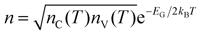 ,20 where nC(T) and nV(T) are the density of electrons and holes in the CB and the VB, respectively and kB is the Boltzmann constant.
As a result, the electric conductivity can be written as
| σ ∼ qμe−EG/2kBT, | (2) |
2.2 Modifications of band theory: the Mott–Davis (MD) amorphous semiconductor model
The word amorphous, for the case of both inorganic and organic solids, refers to the presence of long-range (extended) disorder. For inorganic materials, structural disorder originates from fluctuations of the bond length and the presence of interstitial defects and vacancies. In organic amorphous materials, positional disorder originates, for instance, from shorter (or longer) than average conjugation lengths of molecular chains not arranged into periodic structures.18–21 Twists of molecular backbones are an additional source of disorder (i.e. conformational disorder).26,27A key aspect to understand the transport physics of amorphous systems is that disorder strongly localizes the electronic states. The most accredited description of the electrical properties of amorphous semiconductors is given by the Mott–Davis (MD) model.22 According to it, disorder confines Bloch's waves around a few lattice units and introduces band tails of states at the band edge of VB (EVBE) and CB (ECBE). These states extend in the gap around εF with a Gaussian distribution (shaded blue area, Fig. 1D). In crystals, only band-like conduction is expected because EG is the only activation energy appearing in the analytic expression for σ(T). Conversely, for amorphous solids, several activation energies exist, each one corresponding to a given transport mechanism. For instance, a localized electron can hop to its closest localized empty state (the nearest neighbor hopping (NNH)) or to an empty localized state further away but within the energy landscape around the εF level (variable range hopping (VRH)). For an electron to hop from a fully occupied localized state to an unoccupied localized state, it requires an activation energy such that the conductivity is described by the following equation:
σ = A![[thin space (1/6-em)]](https://www.rsc.org/images/entities/char_2009.gif) exp(−B/Tk) exp(−B/Tk) | (3) |
By applying strong electric fields (e.g. thousands of V cm−1 as in resistive switching experiments) and/or by increasing the temperature, electrons can hop from the occupied localized states, located within ECBE and εF, to empty the delocalized states in the CB (band-like conduction, Fig. 1D).21 The conductivity in the band-like conduction regime is temperature-dependent through an exponential relation similar to eqn (3) but with the exception that k = 1 and B indicates the minimum required energy for the electrons to hop from the localized to delocalized states. The same discussion holds for hopping of holes in the localized states (NNH and VRH) and from the localized to delocalized states beyond the VB (hole band-like conduction).
2.3 Relevance and limitations of the MD model to bio-sourced materials
The relevance of the MD model to bio-sourced materials is an open debate in the field of organic electronics. In biomaterials, the presence of intrinsic and extrinsic (e.g. adsorbed water in the molecular structure) disorder impacts their charge transport properties. Particularly, it has been reported that the presence of adsorbed water perturbates the structural environment of these systems by locally changing the dielectric constant and the capacitance.28 In addition, the interplay of hydration and temperature effects makes the assignment of an exclusive temperature (or hydration)-dependent analytical expression challenging for the electrical conductivity of bio-sourced materials. Despite these complications, several studies on proteins,29 dry and hydrated hemoglobin30 and DNA28,31–34 have showed that the conductivity in these systems is strongly temperature-dependent through hopping of electrons across activation energy barriers, in analogy to amorphous semiconductors. In accordance with these studies, the mobility for mixed electronic–protonic bio-molecular systems can be described as follows:| μ = μ0exp(−EH/kBT) | (4) |
From these considerations, the question whether in bio-sourced materials the band theory of transport holds for ions and for the special case of protons naturally arises. In quest of distinguishing between semiconducting and non-semiconducting bio-sourced materials, accounting for the main type of charge carrier may not be the right approach. As we shall see in Section 3, studies on proton transport mechanisms in protonic biomaterials lead to the concept of protonic semiconductors. The existence of these models calls for a new and holistic definition of semiconductivity for bio-sourced materials.
3. Protonic transport in bio-sourced materials
Biomaterials are intrinsically ionic and wet. Biological signals naturally arise from the movement of ions (e.g. Na+, K+, Ca2+, and Cl−) and protons (H+). In these systems, the presence of ionic species affects the charge transport properties by locally modifying the molecular environment, which is intensely dependent upon the hydration/solvation conditions.Protons are the most mobile charges among ionic species with a close radius and similar mass.39 In nature, protonic transport plays a pivotal role in several biological energy conversion processes, which occur via protonation/de protonation reactions across hydrogen (H) bonds. The most common example is the formation of adenosine triphosphate (ATP) via oxidative phosphorylation of adenosine diphosphate (ADP), driven by proton gradients during photosynthesis in mitochondria.40,41 Additional examples include proton gradients in rhodopsin,42 proton activated flagella in a few species of bacteria,43 and pH regulation in cellular proton channels.44
Aside from specific biological functions, protonic (ionic) transport arouses tremendous interest in the field of organic bio-sourced iontronics. Particularly, protonic (ionic) and mixed conductors can be integrated into logic circuits to mimic, register and stimulate biological functionalities.45,46 Besides converting biochemical (ionic) into electronic signals,47 they can be active components in bioprotonic field-effect transistors,48 light-emitting diodes11 and switching memory devices.49,50 Therefore, understanding the role and the impact of mixed transport on the mesoscopic properties of bio-sourced materials is the underpinning to designing and developing high performance (bio) electronic devices. In protonic and mixed protonic–electronic biomaterials, H-bonds build up molecular chains that serve as pathways for protons.
Herein, we first discuss the fundamental aspects of proton transport mechanisms (e.g. vehicle and Grotthus) in hydrated protonic bio-conductors (Section 3.1). Afterwards, we present the concept of protonic semiconductors by means of the recently developed quantum mechanical description of protonic transport in H-bonded chains of proton conductors (Section 3.2). In the forthcoming section, we discuss the experimental techniques commonly used to measure the flow of protonic currents in bio-sourced conductors (Section 3.3). We then present the examples of a few bio-protonic devices whose working principles are explained by the protonic semiconductor model (e.g. protonic p–n junctions, field-effect transistors and light-emitting diodes, Section 3.4).
We conclude with a special case of eumelanin, a mixed conductor, which for decades has been described as an amorphous semiconductor and only recently considered a predominant proton conductor with the limited contribution of electronic transport to conductivity.
In Section 2, we raised the questions whether the MD model could be applied to bio-sourced conductors and whether the definition of semiconductivity can be extended to protonic and mixed protonic–electronic conductors. We tentatively try to answer these questions by discussing the intriguing case of the biopigment eumelanin (Section 3.5).
3.1 Proton transport mechanisms
H-bonding is a noncovalent and directional interaction where a H atom is shared between two electronegative atoms that take part to form a covalent bond. Due to different bonding configurations, many types of H-bonds exist, approaching a typical energy range from 0.05 eV (i.e. van der Waals bonds) to about 0.7 eV (i.e. covalent bonds).51 In several hydrated bio-sourced materials, molecular chains known as proton wires form via H-bonding between water molecules and between water molecules and proton donor (e.g. N–H, NH2) and/or proton acceptor (e.g. O–H,![[double bond, length as m-dash]](https://www.rsc.org/images/entities/char_e001.gif) O) functional groups. The acidity increases with the content of proton donors and the basicity with the content of proton acceptors.52 The acidity and basicity can also be increased upon hydration, i.e. the increase of water %w/w via water absorption in the molecular backbone.
O) functional groups. The acidity increases with the content of proton donors and the basicity with the content of proton acceptors.52 The acidity and basicity can also be increased upon hydration, i.e. the increase of water %w/w via water absorption in the molecular backbone.
Depending on the level of acidity/basicity (and/or hydration), two hopping mechanisms are possible for protonic transport along the proton wires. At low acidity/basicity (and/or hydration), sequential hops take place via diffusion processes induced by the local charge gradient concentration (vehicle mechanisms). In vehicle mechanisms, the diffusion coefficient (D) depends on the frequency of proton hopping; and the proton mobility (μ) and conductivity (σ) are given by the Einstein–Stokes relations:53
| μ = qD/kBT | (5) |
| σ = nqμ = nq2D/kBT | (6) |
At high acidity/basicity (and/or hydration), proton wires form continuous pathways such that cooperative proton transport via the Grotthus mechanism takes place (Fig. 2A).54,55 In the Grotthus mechanism, the injected protons (H+) and hydroxyl ions (OH−) (considered as ionic defects, with respect to conventional electronic charge carriers) can hop from one molecular site to another (Fig. 2A and B). Each hopping event locally modifies the charge neutrality along the chain. Consequently, a sequence of hopping events can occur only if the molecule donating (receiving) the ionic defect rotates to reverse the direction of its dipole moment. As soon as a rotation occurs, the H-bond losing (receiving) a proton generates an orientational negatively (positively) charged defect, i.e. Bjerrum L (Bjerrum D) in which no protons (two protons) are shared in the H-bond (Fig. 2C). In this framework, the fast-cooperative proton transport is driven by the sequential motion of ionic and orientational defects along the proton wires. The generation and translation of ionic and orientational defects requires energy that can be provided to the system by applying an electric field and/or by raising the temperature. Considering the contribution of the Grotthus transport and vehicle mechanism together, the protonic conductivity can be written as follows:
| σ = nqμ = (C/kBT)exp(−Ea/kBT) | (7) |
 | ||
| Fig. 2 (A) Hopping and reorientation of H-bonded chains in Grotthus's theory of transport (reproduced with permission from ref. 54, copyright (2006) Elsevier); (B) ionic and (C) orientational defects in H-bonded proton wires containing water molecules (reproduced and adapted with permission from ref. 68, copyright (2014) European Geosciences Union); (D) schematic representation showing the double-well potential of the quantum model for Grotthus transport and the sequence of proton hopping events between H-bonded molecules in chains forming proton wires. Protons and water molecules are represented by black and blue circles, respectively. | ||
It is worth noticing that there is a similarity between eqn (3) and (7) (Section 2) for the transport physics of amorphous semiconductors, experimentally verified for a wide range of biological systems and bio-sourced materials, including mixed conductors.28,30,33,56,57
3.2 Protonic semiconductor model
The concept of protonic semiconductivity was formulated for the first time in 1958 after the experimental observation of p–n rectification effects in ice crystals doped with donor–acceptor functional groups.58 p–n rectification effects as well as the p and n-type field-effect behavior of chitosan films have been recently reported by M. Rolandi's group.13 These observations, paralleled by recent quantum mechanical models,57–60 led us to describe the protonic transport in proton wires by considering H+ and OH−, respectively, as the electron and hole counterparts of electronic semiconductors. In this framework, the protons occupy the protonic valence band leaving the protonic conduction band empty, in analogy to the intrinsic semiconductor case. The protonic band gap corresponds to the energy required to generate a proton–proton hole pair. As in the case of electronic intrinsic semiconductors, such an ensemble of proton wires is poorly conductive because the energy required to excite a proton to the conduction band is about two orders of magnitude higher than the room temperature thermal energy (kBT ∼ 25 meV). However, the conductivity of proton wires can be enhanced by injecting ionic defects into them. This process is in analogy with the case of electronic semiconductors, where the addition of electron donor or electron acceptor groups transforms intrinsic semiconductors into n or p type extrinsic ones (doped).20 In a similar fashion, proton wire is doped with proton donor–proton acceptor groups to obtain n–p type wires. Upon n (p) doping, the proto chemical potential, conceptually equivalent to the electronic Fermi energy level, shifts from mid gap toward the protonic conduction (valence) band edge.As previously mentioned, this phenomenological description of protonic transport is well explained by quantum mechanics, as for electronic transport in band theory.22 In this context, the protonic energy levels are determined by considering the proton in the potential of the lattice made of H-bonded water molecules (Fig. 2D). The problem considers the displacement of protons and water molecules as well as mutual interactions in the system (i.e. proton–water molecule and water molecule–water molecule interactions, including the dipole–dipole ones generated by the perturbation of charge neutrality in the chain).
Intuitively, the range of periodicity and the spatial coherence of the lattice potential strongly depend on the total concentration of proton wires available for transport. The proton can be found in two degenerate ground states of a double-well potential separated by a barrier which represents the energy required for the proton to hop across two equilibrium positions in the H-bond (intra-bond barrier, black arrow, Fig. 2D). The second barrier represents the energy required to rotate the molecule and reverse its polarity to eventually generate a Bjerrum defect (inter-bond barrier, red arrow, Fig. 2D). Therefore, the protonic valence band is equivalent to the ensemble of energy levels (i.e. potential wells) generated by the H-bonded water molecules. If no energy is provided to the system, these levels are fully occupied by protons sitting in the double-well.
On the other hand, e.g. by applying an electric field, the Hamiltonian of the quantum system admits the propagation of two delocalized wavefunctions. Depending on the direction of the electric field, a delocalized positive (negative) wavefunction is generated from the overlap between the wavefunctions of positive (negative) ionic and orientational charge defects.59,61
In this view, the definition of the protonic conduction band given by M. Rolandi's group48 as the “excess of protons fluctuating between hydrogen bonds” naturally arises from the delocalized character of the protonic wavefunction.
In conclusion, the protonic semiconductor model can be potentially extended to any bio-sourced materials featuring a significant presence of H-bonded molecular chains, e.g. by absorbing water molecules through hydration.40,55,62,63 As we shall see in detail in Section 3.4, the protonic semiconductor model can nowadays explain the working principles of protonic field-effect transistors (FETs), p–n junctions and light-emitting diodes, i.e. the devices based on H+/OH− doped bio-sourced conductors.11,13,64
3.3 Measuring electronic and protonic currents in bio-sourced materials
Good contacts and efficient charge transfer processes (injection) at the electrode/active layer interface are essential requirements for carrying out reliable charge transport studies and developing optimized architectures for high-performance devices. For electronic conductors, electron/hole injection at metal electrodes (e.g. gold (Au), aluminum (Al), copper (Cu), platinum (Pt), palladium (Pd) and silver (Ag)) is affected by energy band-bending.20 In other words, an offset exists between the metal work function and the valence (highest occupied molecular orbital (HOMO))-conduction band (lowest unoccupied molecular orbital (LUMO)) edge levels of the electronic conductor. This energy mismatch causes the formation of energy barriers due to electron/hole injection, known as the Schottky barrier.20 Schottky barrier effects can be considerably reduced by tuning the metal work function e.g. via chemical functionalization65 or, as recently demonstrated, by using carbon nanotube (CNT)-based electrodes.66The choice of using metal electrodes to measure protonic currents, both for protonic and mixed conductors, entails several challenges. Indeed, metal electrodes do not effectively transfer protons at the contact/active layer interface; they are known as ion (proton)-blocking electrodes. The electron and proton transfer across this type of interface occurs with variable efficiency, i.e. from complete blocking (lowest efficiency) to ohmic injection (highest efficiency).55
During charge carrier injection, chemical reactions may occur at the metal/active layer interface, causing blocking effects and unbalanced charge injection rates. These two effects cause polarization of the metal electrodes and the formation of space charge layers at the interface (defined as the accumulation of charge carriers in a region of the space). The application of moderate or high electric fields can cause discharge effects in the form of space charge currents in the protonic (ionic) conductor. It is important to notice that space charge currents can also flow in amorphous electronic conductors between metal electrodes because their disordered nature favors charge trapping phenomena facilitating injection at the interface.21 In this regard, our group recently found evidence of exclusive electronic transport for dry Sepia melanin pellets, pressed between copper and stainless steel electrodes.67 Thus, at least for mixed conductors, the formation of space charge layers during direct current measurements (DC) is not conclusive to disentangling the single contribution of different carrier types (e.g. protonic/ionic versus electronic) to the total electrical conductivity.
DC measurements of protonic conductors between blocking electrodes should be accompanied by alternate current (AC) measurements i.e. impedance spectroscopy (IS).39,55 In principle, IS measurements can distinguish between protonic (ionic) and electronic contributions to the conductivity of a mixed protonic/electronic conductor between ion-blocking electrodes. By means of IS, the impedance of the system is acquired by applying a small amplitude AC excitation (typically 1–10 mV), while sweeping the frequency over a defined range (i.e. from MHz to mHz). The experimental results are then usually given in terms of the Nyquist plot, where the negative imaginary part of the impedance (−Im(Z)) is plotted against its positive real counterpart (Re(Z)). In this way, direct polarization currents are transformed into alternate currents featuring different dielectric relaxation times. Each relaxation time is a signature of a given protonic (ionic)/electronic process (i.e. charge transfer at the interface, charge transport in the bulk of the active layer and diffusion). To each process correspond different values of impedance. Nonetheless, it is challenging to provide an accurate description of the electrical properties of a material using solely IS. Indeed, a major drawback is that the same Nyquist plot can correspond to different circuit configuration models.69 Over the last four decades, researchers have evaluated the protonic and electronic conductivity of biomaterials,29,30,49,57,63,70,71 bio-sourced protonic and mixed protonic–electronic conductors,28,35,37,38,72 using metal electrodes.
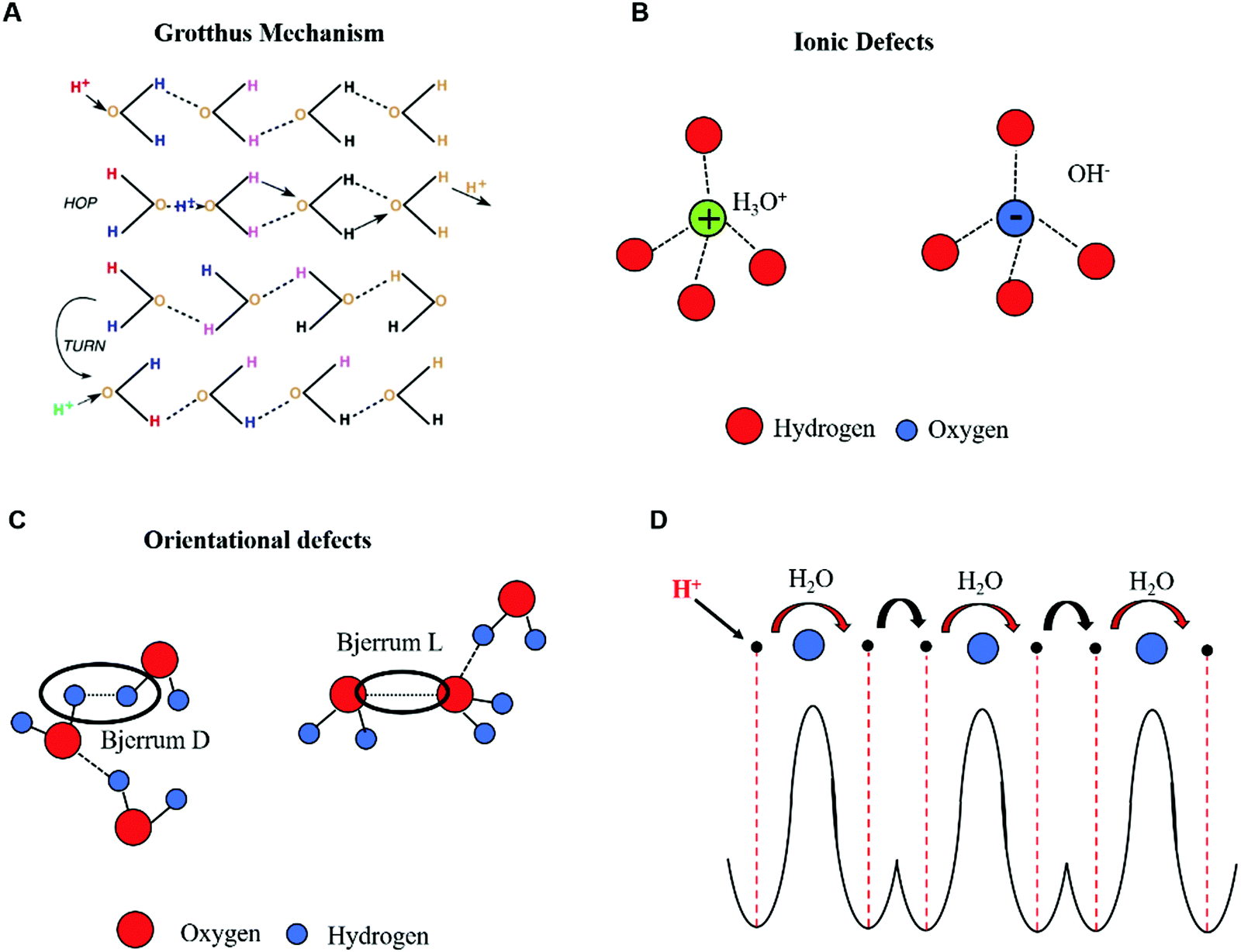
In this regard, Ashkenasy and co-workers recently showed that protonic currents can be efficiently detected with Au and Pd blocking electrodes, especially at high hydration (high relative humidity atmosphere (RH)).73
They measured the electrical response of aβ-Thi peptide thin film proton conductor fibers between Au and Pd electrodes at 60% RH in the presence of water (H2O) and deuterium oxide (D2O). The I–V curves of the fibers hydrated in an H2O atmosphere exhibited higher currents with respect to those hydrated in a D2O atmosphere (Fig. 3A). Remarkably, the conductivity of the fibers hydrated in a D2O atmosphere was lower than that of the fibers hydrated in a H2O atmosphere by a factor of 50. These results indicate that the detected currents were of protonic nature because of the higher proton mobility with respect to the deuterium mobility. The conversion of protonic into electronic currents at the external circuit (inset, Fig. 3A) was explained in terms of undesirable electrochemical processes responsible for water splitting and proton depletion (generation) at the metal cathode (anode)/active layer interface. Gorodetsky et al. investigated the AC response of thin films of the protein reflectin included between the Au electrodes at 90% RH and measured the lower impedance in the films hydrated by H2O vapor with respect to those hydrated by D2O vapor (Fig. 3B).71
 | ||
| Fig. 3 (A) I–V response of aβ-Thi peptide fibers measured with Au and Pd electrodes (6 μm interelectrode distance) at 60% RH with a H2O and D2O atmosphere. The top inset shows the electric circuit used for electrical measurements along with the 5 μm × 5 μm AFM image of the fibers whilst the bottom inset shows the dependence of the current on the voltage sweep rate (reproduced and adapted with permission from ref. 73, copyright (2018) American Chemical Society (ACS)); (B) impedance spectroscopy response of reflectin thin films measured with Au electrodes patterned on SiO2 (50 μm interelectrode distance) with a H2O and D2O atmosphere. The electrode geometry is shown in the inset (reproduced and adapted with permission from ref. 71, copyright (2014) Nature Publishing Group); (C) a schematic example of a two terminal-device with a PdH source and drain protodes connected to maleic chitosan, whose molecular structure is shown in the inset (reproduced and adapted with permission from ref. 13, copyright (2013) Nature Publishing Group); (D) I–V response of maleic chitosan measured with PdH contacts (6 μm interelectrode distance) at different relative humidity levels (reproduced with permission from ref. 64, copyright (2011) Nature Publishing Group); the electrical response of chitosan thin films hydrated at 75% RH with (E) PdHx and (F) Pd electrodes. The legend shows different interelectrode distances in the micrometric scale (reproduced and adapted with permission from ref. 76, copyright (2013) Royal Society of Chemistry (RSC)). | ||
To get rid of ion-blocking effects when acquiring DC in bio protonic devices, the use of contacts capable of (i) injecting (drain) H+ at the source (drain) active layer/contact interface and (ii) transporting electrons towards the external circuit is paramount. These types of contacts are often referred to as protodes. Palladium has been widely used as a proton source because of its ability to inject and extract protons as well as conduct electronically.13,48,55,64,74,75 Palladium forms proton conducting palladium hydride (PdHx) protodes upon exposure to a molecular hydrogen atmosphere.
Protonic and electronic transport across the PdH/active layer interface and in the bulk is monitored by keeping the protodes under a constant H2 atmosphere during the acquisition. This operation ensures the presence of a pool of protons during the measurements. Therefore, palladium hydride protodes act as a proton source (or proton sinks) in a hydrogen atmosphere. Accordingly, PdHx injects protons into the active layer at the source terminal and extracts protons from the channel at the drain terminal (Fig. 3C). The flow of protonic currents is monitored because for each proton exchanged with the active layer an electron is exchanged with the external circuit. This mechanism has been well illustrated by Rolandi's group. They measured the protonic conductivity of maleic chitosan deposited on SiO2 and included between PdHx terminals, showing that the conductivity of maleic chitosan increased with the increase of absorbed water upon hydration (Fig. 3C and D).13,64 The same group compared the protonic currents for the hydrated chitosan films sandwiched between PdHx electrodes and Pd contacts.76 Direct current measurements were done by enclosing the samples in a chamber with controllable relative humidity (ca. 75% RH). The I–V response, acquired from 0.2 V to 1 V, featured higher currents with PdHx than with Pd contacts (Fig. 3E and F).
Our group measured the electrical response of hydrated eumelanin films deposited between coplanar Pd and PdHx protodes.75 Transient current measurements were done at 0.5 V and at relative humidity between 60% RH and 80% RH. The I–V response at all RH showed higher steady state currents with PdHx with respect to Pd contacts. Our results pointed the predominant protonic transport for eumelanin films at high relative humidity.
In conclusion, the extensive body of work herein reported shows that PdHx electrodes are suitable for detecting protonic currents as well as for disentangling protonic and electronic contributions to the electrical conductivity of bio-sourced conductors.64,71,75
3.4 Protonic semiconductor model: from bio-protonic rectifiers to field-effect transistors and light-emitting diodes
Nature “speaks the language of protons and ions”: in many biological systems, electrical signals propagate through the modulation of ionic and protonic currents rather than electronic currents. Bio-sourced protonic and mixed protonic/electronic conductors are widespread in flora and fauna. Despite such ubiquity, only a few examples of protonic devices have been currently demonstrated. In this section, we briefly discuss the recent advances on the design and development of a few bio-sourced protonic conductor-based devices i.e. protonic rectifiers, protonic field-effect transistors (FETs) and protonic light-emitting diodes (PLEDs). The protonic semiconductor model, described and revisited in the previous sections, explains the working principles of these devices where the flow of protonic currents is controlled using an electric field analogous to the electrons and holes in electronic semiconductors.The holistic description of the working principles of these devices is based on the following assumptions, in accordance with the protonic semiconductor model: (i) the active material (e.g. the channels in FETs and biopolymeric junctions in rectifier diodes and PLEDs) is a protonic semiconductor. The band gap of the active material corresponds to the energy required to produce a proton–proton hole pair; the activation energy for cooperative proton transport along the hydrogen bonds connecting several proton wires is approximatively equal to the energy required to break a H-bond (ca. 0.1 eV) (i.e. Grotthus mechanism, Sections 3.1 and 3.2); (ii) the conductivity of the active material increases upon injecting protons and proton-holes by applying an external electric field, performing chemical doping or both. Chemical doping involves functionalizing the molecular backbone of an active material with acidic (H+ donors) or basic (H+ acceptors) groups. If the active material is hygroscopic, doping can also be performed by exposing it to water vapour (i.e. hydration). Water absorption into the molecular structure forms H-bonded pathways between the water molecules and hydrophilic residues of the active material's backbone. As we shall see later, one of the most interesting examples of water-based doping is observed in the case of eumelanin, for which the presence of water has a terrific impact on the electrical properties;36 (iii) upon doping, the density of the charge carriers of proton wires (e.g. protons in the protonic conduction band and proton-holes in the protonic valence band) increases akin to the case of n-type and p-type extrinsic semiconductors.20 As a consequence, the proto chemical potential shifts from its equilibrium position to a position near the protonic conduction (valence) band edge. For protons, the new position of the proto chemical potential μH+ (not to be confused with the proton mobility!) is predicted using the Nernst equation as follows:13
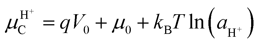 | (8) |
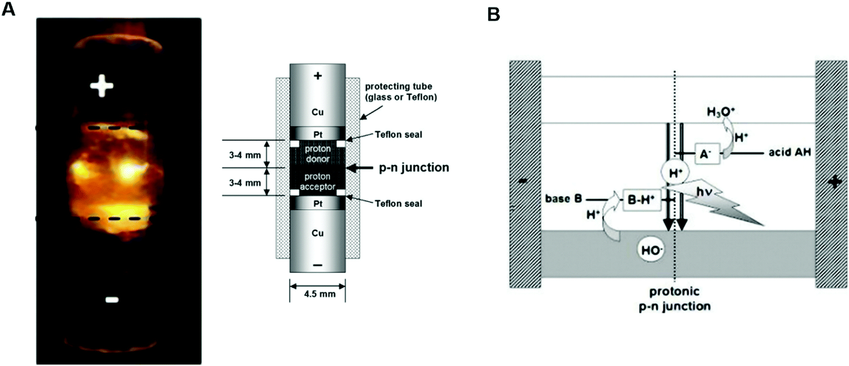
The first attempt to assemble a protonic p–n junction dates back to 1958 when Eigen and De Mayer classified ice as the first natural protonic semiconductor.58 The protonic rectifier consisted of an active layer of a hydrofluoric acid (HF) ice crystal (proton donor) interfaced with a lithium hydroxide (LiOH) ice crystal (proton acceptor). The active layer, sandwiched between PdHx electrodes, showed appreciable rectification behaviour at a relatively high voltage. The device was conceived as a proof of principle and neither the turn-on voltage nor the breakdown voltage was reported. A few years later, in 1984, Langer's group fabricated p–n protonic rectifiers by interfacing Dowex-50 (Dx50) and Dowex-1 (Dx1) polymers between gold and silver electrodes.77,78 The acidic groups –[SO3H] present in Dx50 make it a proton donor and the basic groups –[N(CH3)3]+OH− in Dx1 make it a proton acceptor.
Quinhydrone was used as an electron-to-proton converter to separate the cathode (negative electrode) and the anode (positive electrode) from the active Dx50/Dx1 layer (inset, Fig. 4A). Under unbiased conditions, the initial charge carrier density gradient causes diffusion of protons into Dx1 and proton-holes into Dx5. During this process, a depletion region forms because the protons and proton-holes accumulate on the Dx1/Dx50 interface. Such a depletion region is conceptually identical to the space charge regions formed in the electronic diodes upon contact between n–p type semiconductors. At equilibrium, the internal electric field generates a potential barrier for further proton (proton-hole) diffusion. The application of a forward bias (i.e. a positive bias at the anode electrode) lowers the diffusion barrier enabling injection of protons (proton-holes) into Dx50 (Dx1) and their diffusion across the junction. For each injected proton, an electron is collected at the metal anode. Such a rectifier diode featured a low turn-on voltage (about 0.1 V) and a relatively high breakdown voltage (about 7 V) (Fig. 4A).
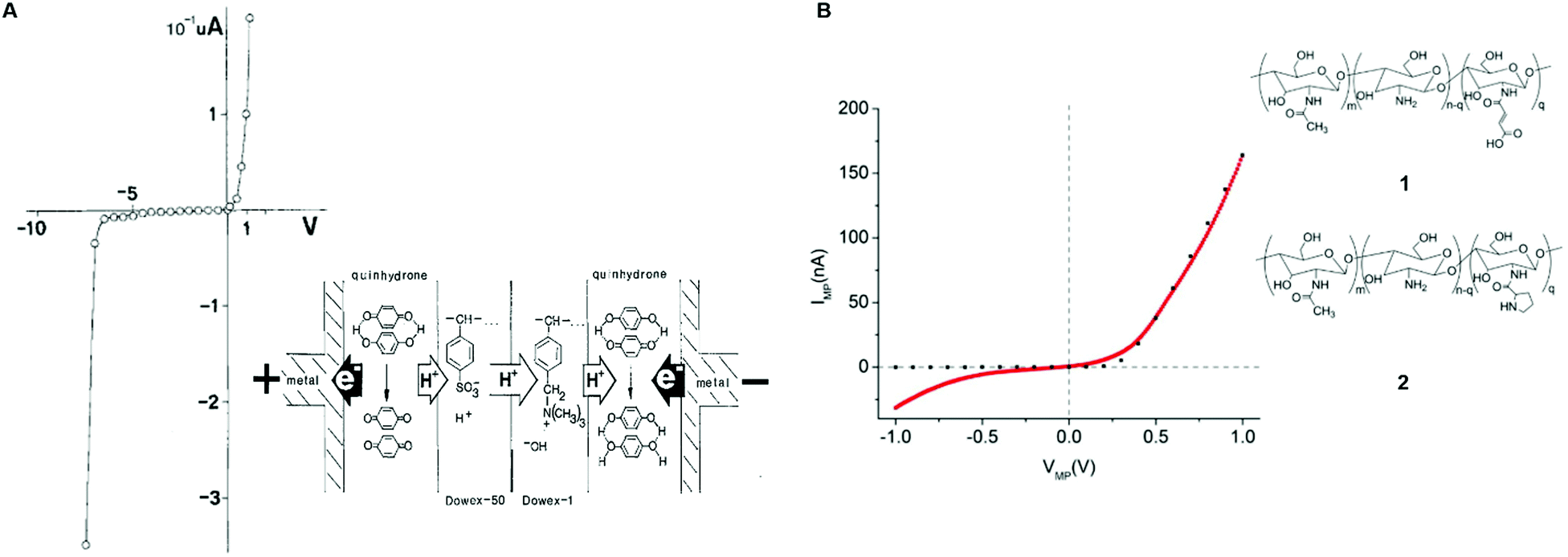 | ||
| Fig. 4 I–V characteristics of (A) Dowex-50 (Dx50)/Dowex-1 (Dx1) (reproduced and adapted with permission from ref. 77, copyright (1985) Springer-Verlag) and (B) maleic/proline chitosan (H+–OH−) rectifiers. Here, the dotted black curve shows the simulated I–V response of a semiconductor-based rectifier (reproduced and adapted with permission from ref. 13, copyright (2013) Nature Publishing Group). In the inset of (A) the rectifier's architecture and its working principle are shown. In the inset of (B) the molecular structure of maleic (1) and proline chitosan is shown (2). | ||
Rolandi's group assembled a chitosan-based rectifier using PdHx contacts.13 Chitosan is a bio-sourced, biodegradable, hygroscopic protonic conductor that can be n (H+) or p (OH−) type doped via chemical functionalization (maleic-chitosan and proline chitosan, respectively 1 and 2, inset Fig. 4B). n-Type maleic chitosan (i.e. H+ rich) was prepared in a mixture of toluene sulfonic acid and formamide solvent, by a one-step chemical reaction between chitosan and maleic anhydride.79 p-Type proline chitosan (i.e. OH− rich) was synthesized by dissolving it into acetic acid and by mixing the obtained solution into a proline 1-ethyl-3-(3-dimethylaminopropyl)carbodiimide (EDC) solution in deionized water.13 The authors evaluated a protonic band gap of about 0.8 eV for maleic and proline chitosan using the Gibbs–Helmoltz's equation:
| Eg = −kBTln(Kw) | (9) |
Maleic and proline chitosan were hydrated at 75% relative humidity (RH), corresponding to 20% and 15% water content by weight. The current (IMP)–voltage (VMP) response of the device featured rectification properties (Fig. 4B) akin to those of the conventional n–p electronic semiconductors. As in the case of the Dx50/Dx1 junction, upon contact between maleic and proline chitosan, proton and proton-hole gradients drive H+ into the proline chitosan and OH− into the maleic chitosan until an equilibrium is reached. Protonic charge carriers thus recombine at the junction to form H2O and create a depletion region at the contact interface with an associated potential difference V0. This potential difference represents the barrier for H+ (OH−) diffusion into proline (maleic) chitosan. The application of a forward bias (i.e. a positive voltage at the H+ side of the rectifier) reduces V0 of a factor −VMP, favouring the flow of current across the junction. The application of a reverse bias (i.e. a negative voltage at the H+ side of the rectifier) increases V0 of a factor +VMP, resulting in low or no current flow. A turn-on voltage of about 0.1 V and a breakdown voltage of about 0.3 V were measured (Fig. 4B).
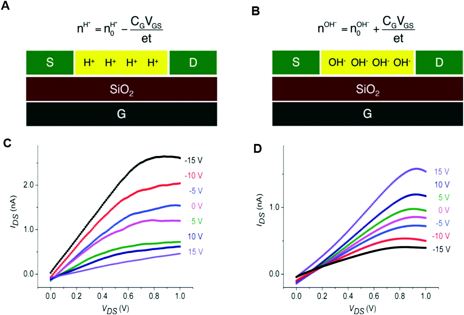
Rolandi's group also showed that maleic and proline chitosan feature protonic semiconductivity as channels on Si-bottom gated FETs (Fig. 5A and B).13,46,64 Maleic and proline chitosan were fabricated following the same protocol used to prepare chitosan-based rectifiers. The n and p-type chitosan were deposited on SiO2 patterned with the PdHx source and drain electrodes. The output characteristics of maleic (proline) chitosan H+(OH−)-FET (i.e. the modulation of the drain–source current (IDS) as a function of drain–source voltage (VDS) at a different gate–source voltage (VGS)) conformed to those of the conventional n-type (p-type) semiconductor-based FET.7,80 Indeed, in the case of maleic chitosan, the application of a negative (positive) VGS results in an increase (decrease) of the channel current IDS and the device can be turned on (off) (Fig. 5C). The increase (decrease) of the current in the channel for negative (positive) VGS originates from the increase (depletion) of positive charge carriers at the maleic chitosan/SiO2 interface. The output characteristics of proline chitosan showed an opposite VGS-dependence (Fig. 5D). As in the case of n (p)-type semiconductors, the total proton/proton-hole density (nH+/OH−) was calculated as follows:
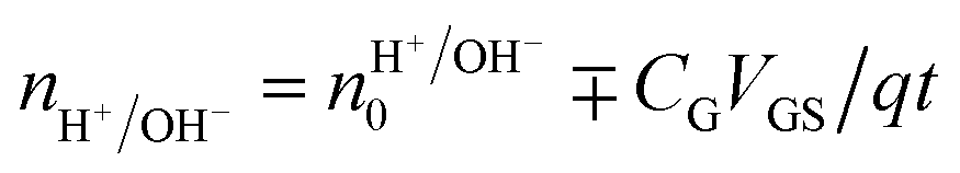 | (10) |
 is the proton/proton-hole density at zero VGS, CG is the gate specific capacitance, t is the thickness of the channel and q is the elementary charge. Maleic and proline chitosan featured an on–off ratio of about 3–4 and a field-effect mobility, respectively, of (5.3 ± 0.5) × 10−3 cm2 V−1 s−1 and (0.40 ± 0.06) × 10−3 cm2 V−1 s−1, which are similar to those reported for hydrated conducting polymers.81
 | ||
| Fig. 5 Schematics (A) and (B) and the output characteristics (C) and (D) of maleic chitosan and proline chitosan FETs, respectively (reproduced and adapted with permission from ref. 13, copyright (2013) Nature Publishing Group). | ||
From the values of the mobility, the authors measured a value of  and
and  of about (8.0 ± 0.4) × 1017 cm−3 and (4.0 ± 0.1) × 1017 cm−3, respectively. The higher field-effect mobility and charge carrier density of maleic chitosan with respect to proline chitosan were explained by the higher water content by weight after hydration for maleic (20% w/w) than for proline chitosan (15% w/w). The results support the hypothesis that maleic and proline chitosan are protonic semiconductors.
Recently, Langer's group designed and developed the first light-emitting diode (PLED) based on protonic conducting materials.11 The active layers of PLEDs were assembled interfacing hydrated proton donor-proton acceptor (H+/OH−) conductors between the Pt electrodes. Dowex-50 (Dx50) and two types of sulfonated crosslinked polystyrenes (SPS) were used as proton donor layers and Dowex-1 (Dx1) as proton acceptor layers. Dx50/Dx1 and SPS/Dx1 PLEDs of about 4 mm-thick were fabricated (Fig. 6A). The emission characteristics (i.e. the dependence of light intensity on the emitted wavelength) featured a broad distribution within the whole vis-NIR range with the maximum centred around 700 nm. Based on quantum chemical studies, the authors related the energy of emission at 700 nm to the protonic band gap. In all the investigated cases, light was emitted far above the device threshold voltage (i.e. within 15 V and 30 V, corresponding to the device currents of about 0.5–0.8 A). The authors excluded any contribution of electrons and/or holes to light generation for the following reasons: (i) light emission was observed only if the active layers were hydrated (i.e. wet) and for the application of a forward bias (i.e. a positive voltage at the anode/the proton donor interface of the rectifier, Fig. 6A). The need of wet active layers and a forward bias for observing light emission is perfectly explained by the protonic semiconductor model. Indeed, similar to what dopants do in electronic diodes, hydration increases the H+ and OH− density, respectively, in the proton donor and proton acceptor wires of active layers, allowing the operation of PLEDs; (ii) light emission occurred in the middle of the junction and not at the Pt/active layer interfaces (Fig. 6A). These results led to conclude that electrons were only involved in H+ and OH− generation at the Pt/active layer interface (polarization).
 | ||
| Fig. 6 (A) Dx50/Dx1 based protonic light emitting diode. Inset shows the schematic of the device; (B) scheme of the light emission in the middle of the junction under the application of a forward bias (i.e. a positive voltage at the proton donor/Pt electrode interface). (Reproduced and adapted from ref. 11, copyright (2020), Royal Society of Chemistry (RSC)). | ||
Accordingly, light generation in PLEDs is due to the synergy between cooperative transport and recombination of highly mobile protons and proton holes in the middle of the junction (Fig. 6B). The above discussion indicates that the protonic semiconductor model is far from being just a theoretical speculation. The existence of functional bio-protonic devices operating just as their electronic counterparts reminds us how subtle and elusive the concept of semiconductivity is for bio-sourced conductors. The extensive body of work herein presented also suggests that the nature of the predominant charge carrier does not rigorously determine whether a bio-sourced material is a semiconductor or not. In the next paragraph, we try to further stress on this idea by briefly reviewing the eumelanin case.
3.5 Mixed protonic–electronic conductors: the case of eumelanin
Among the plethora of bio-sourced conductors available in Nature, eumelanin, a ubiquitous black–brown subgroup of melanin pigments found in flora and fauna, is one of the most fascinating. From a biological point of view, eumelanin has several functions in living organisms, including antioxidant behavior and thermoregulation.82In humans, besides photo-protection, eumelanin is involved in eye, hair and skin coloration as well as in accumulation and release of metal cations in the body.24,25,83 Remarkably, the interactions between iron and neuromelanin (i.e. a red–yellow core–shell pheomelanin–eumelanin pigment84,85) in the human and primate brain have been associated with Parkinson's disease.86 Apart from its biological importance, eumelanin features electronic conjugation (i.e. alternance of single–double carbon bonds), quinone-based redox properties, broadband optical absorption,87,88 free radical scavenging,89 metal-ion chelation,90–92 hydration-dependent electrical response24,36 and photoconductivity.93–96 At the same time, eumelanin is biocompatible97 and possibly biodegradable.98 Eumelanin originates from the oxidative polymerization of 5,6-dihydroxyindole (DHI) and 5,6-dihydroxyindole, 2-carboxylic acid (DHICA). DHI and DHICA organize into heteroaromatic, randomly crosslinked sheets.99,100 The two building blocks have several polymerization sites and co-exist in different quinonoid redox states i.e. hydroquinone (H2Q), semiquinone (SQ) and quinone (Q), (Scheme 1) such that eumelanin features chemical heterogeneity and physical disorder. Because of this heterogeneity, eumelanin can be considered a short-range ordered biopigment (i.e., to a given extent, an organic amorphous material). However, X-ray diffraction (XRD) experiments performed on both natural and synthetic eumelanin evidenced the presence of π–π stacked structures made of sheets of about 15 Å and featuring an interplanar distance of about 3.7 Å.101–103
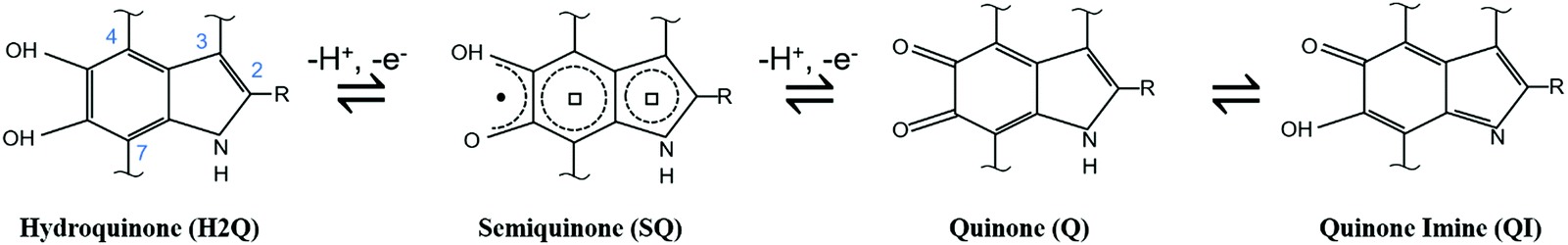 | ||
| Scheme 1 Redox forms of DHI and DHICA eumelanin building blocks. R represents –H in DHI and –COOH in DHICA. | ||
The relative concentration of the H2Q, SQ and Q moieties is regulated by the comproportionation equilibrium, where H2Q and Q react to form hydronium ions and SQ extrinsic free radicals i.e. mobile electronic charge carriers in eumelanin (Scheme 2).37,90,96 The presence of redox groups in the molecular structure and the aforementioned physicochemical properties helps to conceive several eumelanin-based technologies104 including memory devices,105,106 flexible and light assisted-supercapacitors107,108 and phototransistors.12
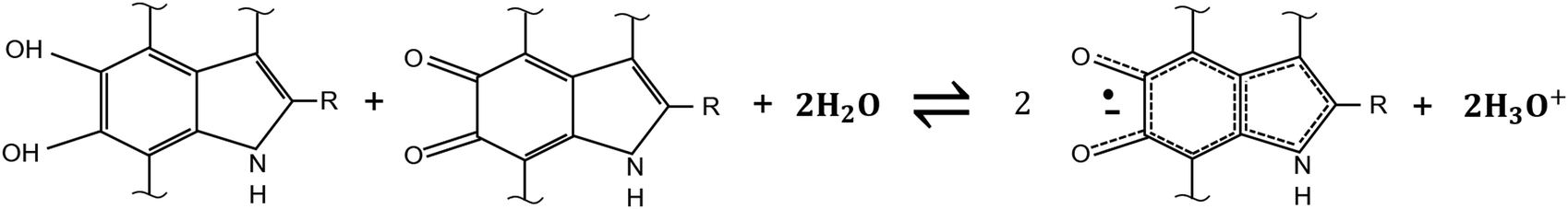 | ||
| Scheme 2 Comproportionation equilibrium regulating the concentration of hydroquinone, semiquinone and quinone forms of DHI and DHICA building blocks. In the presence of water, hydroquinone and quinone react to form hydronium ions (protons) and semiquinone free spins (mobile electrons). | ||
In Section 2.3, we raised the question whether the MD amorphous model, based on the modified band theory (Section 2.2), is an accurate description of the transport physics of bio-sourced materials.
In this context, the case of eumelanin is rather unique and inspiring. For decades the biopigment has been considered an amorphous semiconductor for manifold reasons. Firstly, eumelanin features broadband UV-visible absorption, which in amorphous semiconductors is the consequence of the peculiar density of electronic states (Fig. 1D).109 Secondly, McGinness et al. observed, for synthetic and natural melanin pressed pellets, a reversible electrical resistive switching behavior,35 commonly observed in inorganic amorphous semiconductors (e.g. a-Si, a-Ge, a-Se and a-Te).21,109,110 It is noteworthy that the resistive switching behaviour was observed in a sandwich configuration, regardless of the type of electrical contact (C, Al, and Cu) but only if the powder were hydrated prior to the electrical tests. Remarkably, the pellets obtained from dried powders did not switch. McGinness's results were interpreted with the modified dielectric constant theory formulated by Powell and Rosenberg.28 Accordingly, the presence of water increases the dielectric constant of the material (i.e. by ionizing acid groups). Such an increase lowers the activation energy barrier for charge transport and improves the coulombic screen, leading to resistive switching. Thirdly, the conductivity measurements conducted as a function of temperature performed on eumelanin pellets between 273 K and 343 K111,112 showed an increase of conductivity when the temperature was raised, akin to semiconductors.
A series of landmark studies showed that eumelanin is a photoconductor.93–96 Interestingly, negative photoconductivity was reported for eumelanin pellets (the photoconductivity being broadly defined as the change of the current under illumination (Il − Id) normalized to the value of the current under dark conditions (Id)). The presence of shallow and deep trap states in the band gap of eumelanin, as in the case of amorphous semiconductors, was invoked to explain the observed negative photoconductivity.
Last but not the least, C. J. Bettinger's group97 fabricated solution-processable, biocompatible melanin thin films on silicon dioxide (SiO2) and measured, under hydrated conditions, the electrical conductivity which was about (7.00 ± 1.10) S cm−1, falling in the range of semiconducting materials.
The application of the MD amorphous semiconductor model to eumelanin has been recently questioned in a series of studies published mainly by P. Meredith's group.37,38,47,96,113,114 In these studies, the authors investigated the impact of absorbed water on the transport physics of eumelanin, by studying the water adsorption isotherms of the biopigment (i.e. the effective amount of water adsorbed by weight as a function of atmospheric RH).113,114 They measured the electrical conductivity of eumelanin pellets in sandwich and van der Pauw (vdP) configurations using Au electrodes. The pellets were hydrated in water atmosphere with values of relative humidity ranging from 0% to 90% RH, corresponding to a water content of about 0–20% by weight.
For both the configurations, eumelanin's conductivity increased rapidly if the water content was greater than about 12% by weight (hydration threshold). Particularly, the conductivity vs water content in the sandwich geometry (Fig. 7A) fitted the MD model whilst the vdP one did not (Fig. 7B). Such a discrepancy was explained assuming that in the sandwich geometry, the eumelanin pellets did not reach the hydration equilibrium because only the sides of the pellets were exposed to water vapor. Afterwards, focus was given on probing the microscopic nature of the charge carriers in the eumelanin pellets as a function of hydration and illumination. To this purpose, Mostert et al. performed muon-spin relaxation spectroscopy (μSR)37 and photoinduced electron paramagnetic resonance spectroscopy (p-EPR) surveys on the eumelanin pellets.96 The results evidenced that the (i) μSR spectra were mainly associable to the proton signature at higher water content; (ii) both proton and SQ free spin populations (i.e. electronic charge carriers) increased with the increase of water content; and (iii) protonic and electronic charge carrier hopping rate did not change with the increase of water content. According to these observations, eumelanin was not associated with the amorphous semiconductivity anymore and was rather described as a mixed electronic–protonic conductor. In a sequence of papers published from 2013 to 2015, our group further confirmed the predominance of protonic over electronic transport for highly hydrated eumelanin films in a co-planar configuration between Pt and PdHx electrodes.72,75 Therefore, the MD model for eumelanin was essentially ruled out because of the predominant protonic nature of the transport physics of eumelanin at high water content. In Mostert's frame, water absorption causes, quoting the authors, a “chemical self-doping” where electrons (in the form of SQ) and protons are released by shifting the comproportionation equilibrium. Beyond the hydration threshold, water dopes eumelanin and considerably increases the density of charge carriers (protons and electrons). In turn, protons are transported across protonic pathways (proton wires) via the Grotthus mechanism.
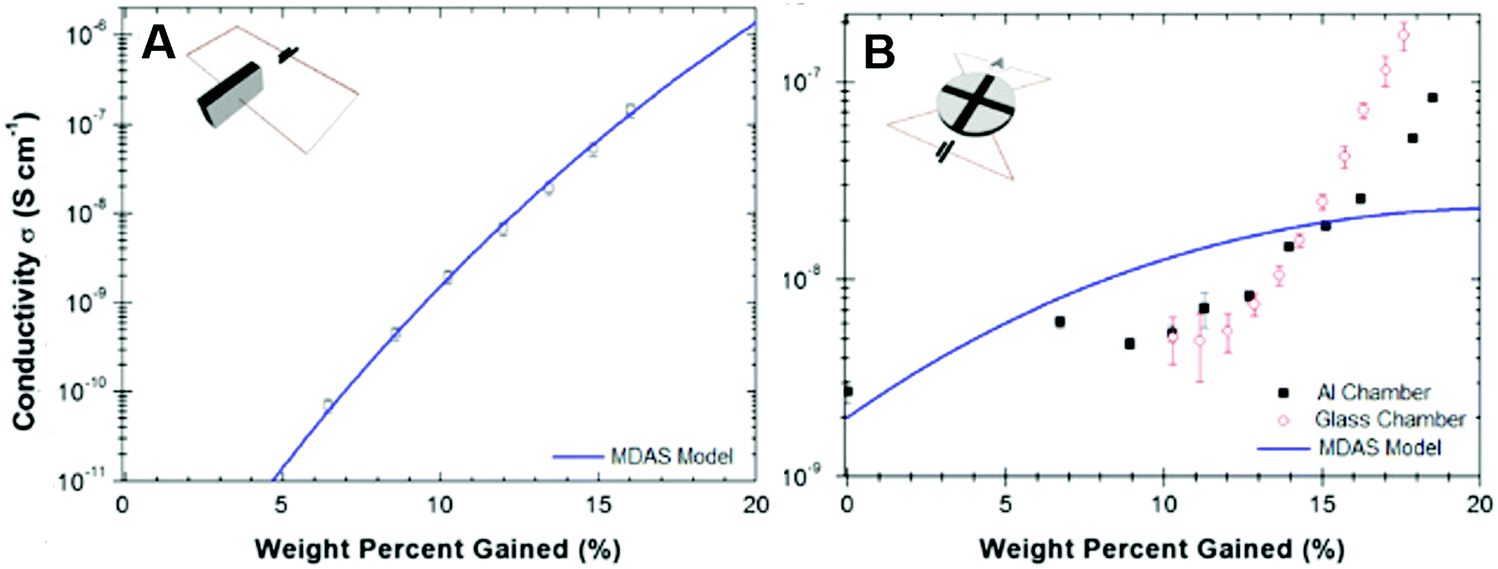 | ||
| Fig. 7 Conductivity as a function of water content by weight for eumelanin pellets (A) in sandwich and (B) van der Pauw geometries (respectively, insets in (A) and (B)). The solid blue line shows the corresponding MD model. (Reproduced from ref. 114, copyright (2012), American Institute of Physics (AIP)). | ||
These studies considerably advanced the knowledge on the impact of adsorbed water on the mesoscopic properties of eumelanin by clarifying the relationship between the microscopic and macroscopic conductivity. Recently, our group reported on the reversible resistive switching behavior of dry and wet Sepia melanin pellets in a sandwich configuration between copper and stainless-steel electrodes (Fig. 8A and B).67 In accordance with the body of work herein presented, we focused on the electrical properties of eumelanin pellets at the opposite sides of the hydration scale (i.e. highly hydrated (19% w/w) vs. dry pellets).
 | ||
| Fig. 8 Resistive switching behaviour at a voltage scan rate of 100 mV s−1 of (A) dry and (B) wet Sepia melanin pellets in a sandwich configuration between copper and stainless-steel electrodes. Insets in (A) and (B), respectively, show the formation of electronic and ionic (protonic) double layers under bias, leading to resistive switching in both cases. (Reproduced and adapted from ref. 67, copyright (2020) American Chemical Society (ACS)). | ||
By combining I–V voltage sweeps at different voltage scan rates, transient current measurements and IS surveys before and after switching, we found strong indications of predominant electronic and protonic transport, respectively, for dry and wet Sepia melanin pellets. We attributed the resistive switching behavior to the formation of electrical double layers of electronic and ionic (protonic) nature for dry and wet pellets, respectively. Assuming the MD model for dry pellets, we proposed that, under the action of the electric field, electronic space charge layers help in charge carrier injection thus shifting eumelanin's Fermi level and consequently improving the overlap of the CB and VB energy states (Fig. 1D and the inset Fig. 8A). Likewise, for wet pellets, the formation under bias of ionic (protonic) double layers increases the proton and SQ free radical density (as per comproportionation equilibrium), leading to resistive switching and band-like conduction (inset, Fig. 8B).
By recalling the fundamentals of the protonic semiconductor model for bio-sourced conductors (Section 3.2), it appears that Mostert's conclusion on the electrical properties of highly hydrated eumelanin describes a doped protonic semiconductor. Our recent results on dry and wet pellets, paralleled by the previous evidence on the support of the electronic and protonic transport model, strongly suggest that the mixed protonic–electronic conductivity of eumelanin is the signature of a special semiconducting behavior. Particularly, depending on the content of adsorbed water, eumelanin appears to “switch” from electronic to protonic semiconductivity. The recent demonstration of a eumelanin-based phototransistor and ion-to electron transducer also appears to support such a fascinating hypothesis.12,47
The instructive case of eumelanin shows that the concept of semiconductivity for bio-sourced materials is elusive. Once again, ascribing semiconducting properties to bio-sourced conductors only longing for the predominant charge carrier (e.g. protons/proton holes and electrons/holes) may bring controversial outcomes. In a completely new perspective, it appears that, for bio-sourced materials, semiconducting properties reflect the presence of quite extended systems of energy bands, regardless of the nature of charge carriers.
4. Conclusions
In this review, we discussed the role of electronic and protonic transport in defining the semiconducting properties of bio-sourced materials. We briefly reviewed the classical band theories for semiconductors, including the MD model for the amorphous ones. We then discussed cooperative proton transport (Grotthus) in protonic and mixed ionic–electronic conductors. Our discussion led us to cast a doubt on the applicability of the “traditional” concept of semiconductivity, based on exclusive electronic transport, to biomaterials. It appears that, for biomaterials, the presence of extended systems of energy bands determines the semiconducting properties rather than the predominant charge carrier type. In this regard, we related the protonic Grotthus transport model with the protonic semiconductor model and presented several complementary bio-protonic based-devices (i.e. FETs, rectifiers and PLEDs), whose working principles are fully explained by this model.We then analyzed the transport physics of eumelanin. The transport models herein reviewed, paralleled by the recent advancements on the electrical properties of eumelanin, suggest that this biopigment would feature both electronic and protonic semiconductivity, the “switching” from predominant electronic to predominant protonic conduction being dependent on the water content of the biopigment.
Nature offers a plethora of solution processable, flexible, conformable, bio-sourced electronic and protonic semiconductors (e.g. indigo, tyrian-purple, epindolidione, quinacridone, and chitosan) promising to design and develop green organic functional devices. In addition, these materials feature electronic and protonic conductivity, as well as biocompatibility, the two key requirements for interfacing biology with conventional electronics. Nowadays, only organic light-emitting diodes have successfully accessed the marketplace (e.g. in TV monitors and laptop screens). In organic semiconductors, air instability and low charge carrier mobility (this last mainly due to the weak nature of the intermolecular interactions and due to intrinsic structural disorder) are among the key factors limiting the high-scale device production. In perspective, we need to extend the current knowledge on the structure–properties relationships of bio-sourced materials by combining theoretical simulations (i.e. density functional theory (DFT)) with supramolecular engineering (e.g. controlling the self-assembly of constituent building blocks as well as tuning the conjugation length and improving the structural order to enhance charge carrier delocalization).
In conclusion, our discussion provides the reader with a holistic description of the charge carrier transport properties of bio-sourced conductors wherein the presence of ionic species, mainly protons, deeply impacts the electrical response. We believe that this review offers new possibilities towards achieving a comprehensive, non-controversial definition of “bio-sourced semiconductors”.
Conflicts of interest
The authors declare no conflicts of interest.Acknowledgements
C. S. acknowledges financial support from NSERC (Discovery grant and Strategic Green Electronics Network: grant number: 513 NETGP 508526-17).Notes and references
- M. Meloni, F. Souchet and D. Sturges, Circular Consumer Electronics: An Initial Exploration, Ellen MacArthur Foundation, 2018, pp. 1–17 Search PubMed.
- C. P. Balde, V. Forti, V. Gray, R. Kuehr and P. Stegmann, The Global E-waste Monitor 2017. Quantities, Flows and Resources, United Nation University, 2017 Search PubMed.
- V. Forti, C. P. Baldé, R. Kuehr and G. Bel, The Global E-waste Monitor 2020: Quantities, Flows, and the Circular Economy Potential, United Nations University, 2020 Search PubMed.
- H. Zhao, D. Waughray, D. M. Malone, J. Msuya, G. Ryder, P. Bakker, N. Seth, L. Yong and R. Payet, World Econ. Forum, 2019, 1–24 Search PubMed.
- M. Irimia-Vladu, Chem. Soc. Rev., 2014, 43, 588–610 RSC.
- M. Irimia-Vladu, E. D. Głowacki, G. Voss, S. Bauer and N. S. Sariciftci, Mater. Today, 2012, 15, 340–346 CrossRef CAS.
- A. Facchetti, Mater. Today, 2007, 10, 28–37 CrossRef CAS.
- M. Irimia-Vladu, Y. Kanbur, F. Camaioni, M. E. Coppola, C. Yumusak, C. V. Irimia, A. Vlad, A. Operamolla, G. M. Farinola, G. P. Suranna, N. González-Benitez, M. C. Molina, L. F. Bautista, H. Langhals, B. Stadlober, E. D. Głowacki and N. S. Sariciftci, Chem. Mater., 2019, 31, 6315–6346 CrossRef CAS.
- A. Facchetti, Chem. Mater., 2011, 23, 733–758 CrossRef CAS.
- N. Thejo Kalyani and S. J. Dhoble, Renewable Sustainable Energy Rev., 2012, 16, 2696–2723 CrossRef CAS.
- J. J. Langer, E. Frąckowiak and S. Golczak, J. Mater. Chem. C, 2020, 8, 943–951 RSC.
- H. J. Nam, J. Cha, S. H. Lee, W. J. Yoo and D. Y. Jung, Chem. Commun., 2014, 50, 1458–1461 RSC.
- Y. Deng, E. Josberger, J. Jin, A. F. Rousdari, B. A. Helms, C. Zhong, M. P. Anantram and M. Rolandi, Sci. Rep., 2013, 3, 1–7 Search PubMed.
- P. Meredith, C. J. Bettinger, M. Irimia-Vladu, A. B. Mostert and P. E. Schwenn, Rep. Prog. Phys., 2013, 76, 034501 CrossRef CAS.
- W. P. Lin, S. J. Liu, T. Gong, Q. Zhao and W. Huang, Adv. Mater., 2014, 26, 570–606 CrossRef CAS.
- S. Pradhan, A. K. Brooks and V. K. Yadavalli, Mater. Today Bio, 2020, 7, 100065 CrossRef CAS.
- M. Wang, P. Baek, A. Akbarinejad, D. Barker and J. Travas-Sejdic, J. Mater. Chem. C, 2019, 7, 5534–5552 RSC.
- N. W. Ashcroft and N. D. Mermin, Solid State Physics, Hartcourt College Publishers, College edn, 1976 Search PubMed.
- C. Kittel, Introduction to Solid State Physics, Wiley J. and Sons Inc., 8th edn, 2005 Search PubMed.
- G. Grosso and G. P. Parravicini, Solid State Physics, Elsevier, Oxford, UK, 2nd edn, 2014 Search PubMed.
- H. Fritzsche, in Amorphous and Liquid Semiconductors, ed. J. Tauc, Plenum Press, London and New York, 1974, pp. 313–355 Search PubMed.
- E. A. Davis and N. F. Mott, Philos. Mag., 1970, 22, 0903–0922 CrossRef CAS.
- X. F. Pang, H. W. Zhang and Z. Jun, Int. J. Mod. Phys. B, 2005, 19, 3835–3859 CrossRef CAS.
- P. Meredith and T. Sarna, Pigm. Cell Res., 2006, 19, 572–594 CrossRef CAS.
- E. Di Mauro, R. Xu, G. Soliveri and C. Santato, MRS Commun., 2017, 7, 141–151 CrossRef CAS.
- R. Noriega, J. Rivnay, K. Vandewal, F. P. V. Koch, N. Stingelin, P. Smith, M. F. Toney and A. Salleo, Nat. Mater., 2013, 12, 1038–1044 CrossRef CAS.
- A. Salleo, in Organic Electronics: Emerging Concepts and Technology, ed. F. Cicoira and C. Santato, Wiley-VCH, 2013, pp. 341–373 Search PubMed.
- M. R. Powell and B. Rosenberg, Bioenergetics, 1970, 1, 493–509 CrossRef CAS.
- B. Rosenberg, Nature, 1962, 193, 364–365 CrossRef CAS.
- B. Rosenberg, J. Chem. Phys., 1962, 36, 816–823 CrossRef CAS.
- D. D. Eley and D. I. Spivey, Trans. Faraday Soc., 1961, 58, 411–415 RSC.
- B. Giese, J. Amaudrut, A. K. Köhler, M. Spormann and S. Wessely, Nature, 2001, 412, 318–320 CrossRef CAS.
- N. P. Armitage, M. Briman and G. Grüner, Phys. Status Solidi, 2004, 241, 69–75 CrossRef CAS.
- C. H. Wohlgamuth, M. A. McWilliams and J. D. Slinker, Anal. Chem., 2013, 85, 8634–8640 CrossRef CAS.
- J. McGinness, P. Corry and P. Proctor, Science, 1974, 183, 853–855 CrossRef CAS.
- M. Reali and C. Santato, in Handbook of Nanoengineering, Quantum Science and Nanotechnology, ed. S. E. Lyshevski, CRC Press, 1st edn, 2019, pp. 101–113 Search PubMed.
- A. B. Mostert, B. J. Powell, F. L. Pratt, G. R. Hanson, T. Sarna, I. R. Gentle and P. Meredith, Proc. Natl. Acad. Sci. U. S. A., 2012, 109, 8943–8947 CrossRef CAS.
- M. Sheliakina, A. B. Mostert and P. Meredith, Adv. Funct. Mater., 2018, 1805514 CrossRef.
- A. J. Bard and L. R. Faulkner, in Electrochemical methods: fundamentals and applications, ed. D. Harris, E. Swain and E. Aiello, Wiley J. and Sons Inc., 2nd edn, 2001, pp. 1–814 Search PubMed.
- J. F. Nagle, M. Mille and H. J. Morowitz, J. Chem. Phys., 1980, 72, 3959–3971 CrossRef CAS.
- H. J. Morowitz, Am. J. Physiol.: Regul., Integr. Comp. Physiol., 1978, 4, R99–R114 CrossRef.
- J. K. Lanyi, Annu. Rev. Physiol., 2004, 66, 665–686 CrossRef CAS.
- D. Walz and S. R. Caplan, Bioelectrochemistry, 2002, 55, 89–92 CrossRef CAS.
- M. Capasso, T. E. DeCoursey and M. J. S. Dyer, Trends Cell Biol., 2011, 21, 20–28 CrossRef CAS.
- T. Arbring Sjöström, M. Berggren, E. O. Gabrielsson, P. Janson, D. J. Poxson, M. Seitanidou and D. T. Simon, Adv. Mater. Technol., 2018, 3, 1700360 CrossRef.
- X. Strakosas, J. Selberg, Z. Hemmatian and M. Rolandi, Adv. Sci., 2017, 4, 1–7 Search PubMed.
- M. Sheliakina, A. B. Mostert and P. Meredith, Mater. Horiz., 2018, 5, 256–263 RSC.
- T. Miyake and M. Rolandi, J. Phys.: Condens. Matter, 2016, 28, 1–11 CrossRef CAS.
- Z. Hemmatian, T. Miyake, Y. Deng, E. E. Josberger, S. Keene, R. Kautz, C. Zhong, J. Jin and M. Rolandi, J. Mater. Chem. C, 2015, 3, 6407–6412 RSC.
- E. E. Josberger, Y. Deng, W. Sun, R. Kautz and M. Rolandi, Adv. Mater., 2014, 26, 4986–4990 CrossRef CAS.
- P. Atkins and J. De Paula, Physical Chemistry, Freeman W.H. and Company, New York, 9th edn, 2010 Search PubMed.
- E. D. Głowacki, M. Irimia-Vladu, S. Bauer and N. S. Sariciftci, J. Mater. Chem. B, 2013, 1, 3742–3753 RSC.
- P. Padma Kumar and S. Yashonath, J. Chem. Sci., 2006, 118, 135–154 CrossRef.
- S. Cukierman, Biochim. Biophys. Acta, Bioenerg., 2006, 1757, 876–885 CrossRef CAS.
- L. Glasser, Chem. Rev., 1975, 75, 21–65 CrossRef CAS.
- D. Porath, A. Bezryadin, S. De Vries and C. Dekker, Nature, 2000, 403, 635–638 CrossRef CAS.
- G. H. Bardelmeyer, Biopolymers, 1973, 12, 2289–2302 CrossRef CAS.
- L. Eigen and M. De-Maeyer, Proc. R. Soc., 1958, 247, 505–533 Search PubMed.
- S. N. Pnevmatikos and G. P. Tsironis, J. Phys., Colloq., 1989, 50, C3-3–C3-10 CrossRef.
- N. Pavlenko, J. Phys.: Condens. Matter, 2003, 15, 291–307 CrossRef CAS.
- S. Pnevmatikos, Phys. Rev. Lett., 1988, 60, 1534–1537 CrossRef CAS.
- D. Hadži, J. Mol. Struct., 1988, 177, 1–21 CrossRef.
- X. Y. Zhang, J. Shao, S. X. Jiang, B. Wang and Y. Zheng, Nanotechnology, 2015, 26, 125702 CrossRef CAS.
- C. Zhong, Y. Deng, A. F. Roudsari, A. Kapetanovic, M. P. Anantram and M. Rolandi, Nat. Commun., 2011, 2, 2–6 Search PubMed.
- D. M. Alloway, A. L. Graham, X. Yang, A. Mudalige, R. Colorado, V. H. Wysocki, J. E. Pemberton, T. R. Lee, R. J. Wysocki and N. R. Armstrong, J. Phys. Chem. C, 2009, 113, 20328–20334 CrossRef CAS.
- I. Valitova, M. Amato, F. Mahvash, G. Cantele, A. Maffucci, C. Santato, R. Martel and F. Cicoira, Nanoscale, 2013, 5, 4638–4646 RSC.
- M. Reali, A. Gouda, J. Bellemare, D. Ménard, J.-M. Nunzi, F. Soavi and C. Santato, ACS Appl. Bio Mater., 2020, 3(8), 5244–5252 CrossRef CAS.
- T. Bartels-Rausch, H. W. Jacobi, T. F. Kahan, J. L. Thomas, E. S. Thomson, J. P. D. Abbatt, M. Ammann, J. R. Blackford, H. Bluhm, C. Boxe, F. Domine, M. M. Frey, I. Gladich, M. I. Guzman, D. Heger, T. Huthwelker, P. Klan, W. F. Kubs, M. H. Kuo, S. Maus, S. G. Moussa, V. F. McNeill, J. T. Newberg, J. B. C. Petterson, M. Roeselova and R. Sodeau, Atmos. Chem. Phys., 2014, 14, 1587–1633 CrossRef.
- V. Di Noto, J. Phys. Chem. B, 2002, 106, 11139–11154 CrossRef CAS.
- M. Amit, S. Appel, R. Cohen, G. Cheng, I. W. Hamley and N. Ashkenasy, Adv. Funct. Mater., 2014, 24, 5873–5880 CrossRef CAS.
- D. D. Ordinario, L. Phan, W. G. Walkup IV, J. M. Jocson, E. Karshalev, N. Hüsken and A. A. Gorodetsky, Nat. Chem., 2014, 6, 596–602 CrossRef CAS.
- J. Wünsche, L. Cardenas, F. Rosei, F. Cicoira, R. Gauvin, C. F. O. Graeff, S. Poulin, A. Pezzella and C. Santato, Adv. Funct. Mater., 2013, 23, 5591–5598 CrossRef.
- M. Amit, S. Roy, Y. Deng, E. Josberger, M. Rolandi and N. Ashkenasy, ACS Appl. Mater. Interfaces, 2018, 10, 1933–1938 CrossRef CAS.
- H. Morgan, R. Petig and G. T. Stevens, J. Phys. E: Sci. Instrum., 1986, 19, 80–82 CrossRef CAS.
- J. Wünsche, Y. Deng, P. Kumar, E. Di Mauro, E. Josberger, J. Sayago, A. Pezzella, F. Soavi, F. Cicoira, M. Rolandi and C. Santato, Chem. Mater., 2015, 27, 436–442 CrossRef.
- J. T. Robinson, J. J. Pietron, B. Blue, F. K. Perkins, E. Josberger, Y. Deng and M. Rolandi, J. Mater. Chem. C, 2017, 5, 11083–11091 RSC.
- J. J. Langer, Appl. Phys. A: Solids Surf., 1985, 38, 59–60 CrossRef.
- J. J. Langer, Appl. Phys. A: Solids Surf., 1984, 34, 195–198 CrossRef.
- C. Zhong, J. Wu, C. A. Reinhart-King and C. C. Chu, Acta Biomater., 2010, 6, 3908–3918 CrossRef CAS.
- H. Sirringhaus, Adv. Mater., 2005, 17, 2411–2425 CrossRef CAS.
- E. Stavrinidou, P. Leleux, H. Rajaona, D. Khodagholy, J. Rivnay, M. Lindau, S. Sanaur and G. G. Malliaras, Adv. Mater., 2013, 25, 4488–4493 CrossRef CAS.
- G. Prota, Pigm. Cell Res., 2000, 13, 283–293 CrossRef CAS.
- Melanins and Melanosomes, Biosynthesis, Biogenesis, Physiological and Pathological Functions, ed. J. B. Patrick and A. Riley, Wiley-Blackwell, Wiley-VCH Verlag & Co. KGaA, Weinheim, Germany, 2011 Search PubMed.
- H. Fedorow, F. Tribl, G. Halliday, M. Gerlach, P. Riederer and K. L. Double, Prog. Neurobiol., 2005, 75, 109–124 CrossRef CAS.
- W. D. Bush, J. Garguilo, F. A. Zucca, A. Albertini, L. Zecca, G. S. Edwards, R. J. Nemanich and J. D. Simon, Proc. Natl. Acad. Sci. U. S. A., 2006, 103, 14785–14789 CrossRef CAS.
- F. A. Zucca, J. Segura-Aguilar, E. Ferrari, P. Muñoz, I. Paris, D. Sulzer, T. Sarna, L. Casella and L. Zecca, Prog. Neurobiol., 2017, 155, 96–119 CrossRef CAS.
- M. L. Tran, B. J. Powell and P. Meredith, Biophys. J., 2006, 90, 743–752 CrossRef CAS.
- C. T. Chen, C. Chuang, J. Cao, V. Ball, D. Ruch and M. J. Buehler, Nat. Commun., 2014, 5, 1–10 Search PubMed.
- H. C. Longuet-Higgins, Arch. Biochem. Biophys., 1960, 86, 231–232 CrossRef CAS.
- C. C. Felix, J. S. Hyde, T. Sarna and R. C. Sealy, J. Am. Chem. Soc., 1978, 100, 3922–3926 CrossRef CAS.
- J. U. Sutter and D. J. S. Birch, Methods Appl. Fluoresc., 2014, 2, 024005 CrossRef.
- L. Hong and J. D. Simon, J. Phys. Chem. B, 2007, 111, 7938–7947 CrossRef CAS.
- P. R. Crippa, V. Cristofoletti and N. Romeo, Biochim. Biophys. Acta, 1978, 538, 164–170 CrossRef CAS.
- M. Jastrzebska, A. Kocot and L. Tajber, J. Photochem. Photobiol., B, 2002, 66, 201–206 CrossRef CAS.
- V. Capozzi, G. Perna, P. Carmone, A. Gallone, M. Lastella, E. Mezzenga, G. Quartucci, M. Ambrico, V. Augelli, P. F. Biagi, T. Ligonzo, A. Minafra, L. Schiavulli, M. Pallara and R. Cicero, Thin Solid Films, 2006, 511–512, 362–366 CrossRef CAS.
- A. B. Mostert, S. B. Rienecker, C. Noble, G. R. Hanson and P. Meredith, Sci. Adv., 2018, 4, 1–6 Search PubMed.
- C. J. Bettinger, J. P. Bruggeman, A. Misra, J. T. Borenstein and R. Langer, Biomaterials, 2009, 30, 3050–3057 CrossRef CAS.
- E. Di Mauro, D. Rho and C. Santato, under review.
- L. Panzella, G. Gentile, G. D’Errico, N. F. Della Vecchia, M. E. Errico, A. Napolitano, C. Carfagna and M. D’Ischia, Angew. Chem., Int. Ed., 2013, 52, 1–5 CrossRef.
- A. Antidormi, C. Melis, E. Canadell and L. Colombo, J. Phys. Chem. C, 2018, 122, 28368–28374 CrossRef CAS.
- J. Cheng, S. C. Moss and M. Eisner, Pigm. Cell Res., 1994, 7, 263–273 CrossRef CAS.
- J. Cheng, S. C. Moss, M. Eisner and P. Zschack, Pigm. Cell Res., 1994, 7, 255–262 CrossRef CAS.
- A. Büngeler, B. Hämisch, K. Huber, W. Bremser and O. I. Strube, Langmuir, 2017, 33, 6895–6901 CrossRef.
- W. Xie, E. Pakdel, Y. Liang, Y. J. Kim, D. Liu, L. Sun and X. Wang, Biomacromolecules, 2019, 20, 4312–4331 CrossRef CAS.
- M. Ambrico, P. F. Ambrico, A. Cardone, T. Ligonzo, S. R. Cicco, R. Di Mundo, V. Augelli and G. M. Farinola, Adv. Mater., 2011, 23, 3332–3336 CrossRef CAS.
- M. Ambrico, P. F. Ambrico, T. Ligonzo, A. Cardone, S. R. Cicco, M. D’Ischia and G. M. Farinola, J. Mater. Chem. C, 2015, 3, 6413–6423 RSC.
- P. Kumar, E. Di Mauro, S. Zhang, A. Pezzella, F. Soavi, C. Santato and F. Cicoira, J. Mater. Chem. C, 2016, 4, 9516–9525 RSC.
- R. Xu, A. Gouda, M. F. Caso, F. Soavi and C. Santato, ACS Omega, 2019, 4, 12244–12251 CrossRef CAS.
- J. Tauc, in Amorphous and Liquid Semiconductors, ed. J. Tauc, Plenum Press, London and New York, 1974, pp. 159–214 Search PubMed.
- D. Kaplan and T. Adler, J. Non-Cryst. Solids, 1972, 8, 538–543 CrossRef.
- M. M. Jastrzebska, H. Isotalo, J. Paloheimo and H. Stubb, J. Biomater. Sci., Polym. Ed., 1995, 7, 577–586 CrossRef CAS.
- M. M. Jastrzebska, S. Jussila and H. Isotalo, J. Mater. Sci., 1998, 33, 4023–4028 CrossRef CAS.
- A. Bernardus Mostert, K. J. P. Davy, J. L. Ruggles, B. J. Powell, I. R. Gentle and P. Meredith, Langmuir, 2010, 26, 412–416 CrossRef.
- A. B. Mostert, B. J. Powell, I. R. Gentle and P. Meredith, Appl. Phys. Lett., 2012, 100, 1–3 Search PubMed.
| This journal is © The Royal Society of Chemistry 2021 |